WO2024257319A1 - Dispositif d'inspection de défauts et système optique - Google Patents
Dispositif d'inspection de défauts et système optique Download PDFInfo
- Publication number
- WO2024257319A1 WO2024257319A1 PCT/JP2023/022332 JP2023022332W WO2024257319A1 WO 2024257319 A1 WO2024257319 A1 WO 2024257319A1 JP 2023022332 W JP2023022332 W JP 2023022332W WO 2024257319 A1 WO2024257319 A1 WO 2024257319A1
- Authority
- WO
- WIPO (PCT)
- Prior art keywords
- pupil
- light
- illumination
- angle
- sample
- Prior art date
- Legal status (The legal status is an assumption and is not a legal conclusion. Google has not performed a legal analysis and makes no representation as to the accuracy of the status listed.)
- Ceased
Links
Images







Classifications
-
- G—PHYSICS
- G01—MEASURING; TESTING
- G01B—MEASURING LENGTH, THICKNESS OR SIMILAR LINEAR DIMENSIONS; MEASURING ANGLES; MEASURING AREAS; MEASURING IRREGULARITIES OF SURFACES OR CONTOURS
- G01B11/00—Measuring arrangements characterised by the use of optical techniques
- G01B11/02—Measuring arrangements characterised by the use of optical techniques for measuring length, width or thickness
- G01B11/06—Measuring arrangements characterised by the use of optical techniques for measuring length, width or thickness for measuring thickness ; e.g. of sheet material
-
- G—PHYSICS
- G01—MEASURING; TESTING
- G01N—INVESTIGATING OR ANALYSING MATERIALS BY DETERMINING THEIR CHEMICAL OR PHYSICAL PROPERTIES
- G01N21/00—Investigating or analysing materials by the use of optical means, i.e. using sub-millimetre waves, infrared, visible or ultraviolet light
- G01N21/84—Systems specially adapted for particular applications
- G01N21/88—Investigating the presence of flaws or contamination
- G01N21/95—Investigating the presence of flaws or contamination characterised by the material or shape of the object to be examined
- G01N21/956—Inspecting patterns on the surface of objects
-
- G—PHYSICS
- G02—OPTICS
- G02B—OPTICAL ELEMENTS, SYSTEMS OR APPARATUS
- G02B5/00—Optical elements other than lenses
Definitions
- JP2014-504370A Patent Document 1
- Patent Document 1 JP2014-504370A
- Patent document 1 describes a configuration "configured to divide the collection numerical aperture (NA) of the collection subsystem into different segments and to direct the scattered light collected in the different segments to separate detectors," and as an example, describes an aperture mirror placed in the Fourier plane of the collection subsystem as "transmitting the scattered light collected in one segment of the collection NA while reflecting the scattered light collected in another segment of the collection NA.” It also discloses technology that suppresses surface scattering from the wafer surface by "configuring the scattered light in one of the different segments to be separated based on polarization into different portions of scattered light.”
- Patent Document 2 in order to detect scattered light generated from minute defects, multiple detection systems are arranged in a direction inclined to the sample surface, and each detection system forms an image of the linear illumination irradiated on the sample surface at the sensor position to determine defects.
- the optical system is arranged so that the image of the linear illumination can be detected from an oblique angle, the working distance between the detection unit and the linear illumination unit on the sample surface changes within the field of view. At this time, a focus shift occurs, and the resolution of the image formed on the sensor surface decreases.
- Patent Document 1 describes that the image on the inspected substrate W can be formed obliquely on the detector by tilting the sensor so that it is conjugate with the inspected substrate W according to the inclination of the detection direction relative to the inspected substrate W.
- the defect inspection used in the manufacturing process of semiconductors and other products requires the detection of minute defects, the measurement of the dimensions of detected defects with high precision, the inspection of the sample non-destructively (i.e. without altering the sample), the obtaining of substantially consistent inspection results in terms of, for example, the number, position, dimensions, and type of defects when inspecting the same sample, and the inspection of a large number of samples within a certain period of time.
- the optical path is branched using an "aperture mirror" on the Fourier plane of the objective lens to discriminate from background scattered light, and for each branched optical path, the optical path is further branched according to the polarization.
- the directions in which scattered light from defects and background scattered light propagate differ depending on the condition of the sample surface being inspected, so the optical path branching conditions that give the highest sensitivity differ.
- the optical path branching conditions that give the highest sensitivity also differ depending on inspection conditions such as the incident direction of the illumination.
- the object of the present invention is to provide a defect inspection device that can achieve optimal optical path branching conditions depending on the inspection object or inspection conditions.
- One example is a defect inspection device having an illumination unit that irradiates the sample with illumination light emitted from a light source, a detection unit that is arranged in an oblique direction with respect to the sample and detects scattered light generated from the sample, a pupil splitting mechanism that splits the pupil of the detection unit into a first detection angle and a second detection angle, a first photoelectric conversion unit that converts the scattered light at the first detection angle detected by the detection unit into an electrical signal, a second photoelectric conversion unit that converts the scattered light at the second detection angle detected by the detection unit into an electrical signal, and a signal processing unit that processes the electrical signals converted by the first photoelectric conversion unit and the second photoelectric conversion unit to detect defects in the sample, and the pupil splitting mechanism splits the pupil so as to achieve a pupil distribution according to the inspection target or inspection conditions.
- the pupil of the detection unit is divided so that its distribution corresponds to the inspection object or inspection conditions, thereby discriminating background scattered light and detecting light scattered from minute defects with high sensitivity.
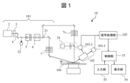
- FIG. 1 is an overall schematic configuration diagram showing an embodiment of a defect inspection device
- 4A to 4C are diagrams illustrating a first example of an illumination intensity distribution shape realized by an illumination unit.
- 4A to 4C are diagrams illustrating a first example of an illumination intensity distribution shape realized by an illumination unit.
- 13 is a diagram showing a second example of an illumination intensity distribution shape realized by the illumination unit.
- FIG. 13 is a diagram showing a third example of an illumination intensity distribution shape realized by the illumination unit.
- FIG. 13 is a diagram showing a third example of an illumination intensity distribution shape realized by the illumination unit.
- FIG. 11A and 11B are diagrams illustrating examples of optical elements included in an illumination intensity distribution control unit.
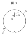
- 1A and 1B are diagrams showing the illumination distribution shape and the scanning direction on a sample surface.
- FIG. 13 is a diagram showing a trajectory of an illumination spot caused by scanning.
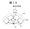
- FIG. 4 is a side view showing the arrangement and detection direction of the detection unit.
- FIG. 4 is a diagram showing the arrangement and detection direction of the detection unit as viewed from above.
- FIG. 4 is a diagram illustrating a first example of the configuration of a detection unit.
- FIG. 2 is a diagram showing the arrangement of illumination spots and photoelectric conversion units.
- FIG. 2 is a diagram showing the arrangement of illumination spots and photoelectric conversion units.
- FIG. 2 is a diagram showing the arrangement of illumination spots and photoelectric conversion units.
- FIG. 2 is a diagram showing the arrangement of a sample and a detection unit.
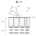
- FIG. 2 is a cross-sectional view of an image sensor.
- FIG. 13 is a graph showing the incidence angle dependence of the absorptance of an anti-reflection film.
- FIG. 13 is a graph showing the incidence angle dependence of the absorptance of an anti-reflection film.
- FIG. 11 is a diagram showing a first example of the pupil division angle dependency of the SNR of scattered light from a defect.
- FIG. 13 is a diagram showing a second example of the pupil division angle dependency of the SNR of scattered light from a defect.
- FIG. 2 illustrates a first example of a knife edge for dividing a pupil.
- FIG. 13 is a diagram showing the configuration of a detection unit in the case of oblique incidence illumination.
- FIG. 13 is a diagram showing the configuration of a detection unit in the case of vertical illumination.
- FIG. 13 shows a second example of a knife edge for dividing a pupil.
- FIG. 11 is a diagram showing a second example of the configuration of the detection unit as viewed from above.
- FIG. 11 is a side view of a second example of the configuration of the detection unit.
- FIG. 11 is a top view of a third example of the configuration of the detection unit.
- 13 is a diagram showing the configuration of a detection unit when detecting different polarized light.
- FIG. 13 is a diagram showing the configuration of a detection unit when the polarization of illumination is changed.
- FIG. 13 illustrates a third example of a knife edge for dividing a pupil.
- FIG. 2 is a diagram showing a drive mechanism of the knife edge.
- FIG. 13 is a side view of a fourth example of the configuration of the detection unit.
- the present invention will be described as being applied to a defect inspection device used in defect inspection carried out in the manufacturing process of semiconductors, etc.
- FIG. 1 is a schematic diagram of the present embodiment.
- the defect inspection device 10 has, as its main components, an illumination unit 101, a detection unit 102, photoelectric conversion units 103-1 and 103-2, a stage 104 on which a sample W can be placed and which can be moved in a direction perpendicular to the surface by an actuator, a signal processing unit 105, a control unit 53, a display unit 54, and an input unit 55.
- the illumination unit 101 appropriately comprises a laser light source 2, an attenuator 3, an emitted light adjustment unit 4, a beam expander 5, a polarization control unit 6, and an illumination intensity distribution control unit 7.
- the laser light beam emitted from the laser light source 2 is adjusted to a desired beam intensity by the attenuator 3, adjusted to a desired beam position and beam traveling direction by the emitted light adjustment unit 4, adjusted to a desired beam diameter by the beam expander 5, adjusted to a desired polarization state by the polarization control unit 6, and adjusted to a desired intensity distribution by the illumination intensity distribution control unit 7, and illuminated onto the inspection target area of the sample W.
- the angle of incidence of the illumination light on the sample surface is determined by the position and angle of the reflecting mirror of the output light adjustment unit 4 arranged in the optical path of the illumination unit 101.
- the angle of incidence of the illumination light is set to an angle suitable for detecting minute defects.
- the larger the illumination incidence angle that is, the smaller the illumination elevation angle (angle between the sample surface and the illumination optical axis), the weaker the scattered light (called haze) from minute irregularities on the sample surface, which becomes noise in the scattered light from minute foreign objects on the sample surface, and the more suitable it is for detecting minute defects.
- the incidence angle of the illumination light is preferably set to 75 degrees or more (elevation angle 15 degrees or less).
- the incidence angle of the illumination light is preferably set to 60 degrees or more and 75 degrees or less (elevation angle 15 degrees or more and 30 degrees or less).
- the polarization control in the polarization control unit 6 of the illumination unit 101 allows the illumination polarization to be P-polarized, which increases the scattered light from defects on the sample surface compared to other polarizations.
- the illumination polarization can be set to S-polarized, which reduces the scattered light from minute irregularities on the sample surface compared to other polarizations.
- the illumination optical path is changed and illumination light is irradiated from a direction substantially perpendicular to the sample surface (perpendicular illumination).
- the illumination intensity distribution on the sample surface is controlled by illumination intensity distribution control unit 7v in the same way as oblique incidence illumination.
- oblique incidence illumination and perpendicular illumination can be performed simultaneously.
- perpendicular illumination that is substantially perpendicular to the sample surface is suitable.
- the laser light source 2 To detect minute defects near the surface of the sample, the laser light source 2 must emit a short-wavelength (355 nm or less) ultraviolet or vacuum ultraviolet laser beam that does not easily penetrate the inside of the sample, and must have a high output of 2 W or more. The diameter of the emitted beam is approximately 1 mm. To detect defects inside the sample, a laser light source that emits a visible or infrared laser beam with a wavelength that easily penetrates the inside of the sample must be used.
- the attenuator 3 is appropriately equipped with a first polarizing plate, a half-wave plate that can rotate around the optical axis of the illumination light, and a second polarizing plate.
- the light incident on the attenuator 3 is converted to linearly polarized light by the first polarizing plate, and the polarization direction is rotated in an arbitrary direction according to the slow axis azimuth angle of the half-wave plate, and passes through the second polarizing plate.
- the azimuth angle of the half-wave plate By controlling the azimuth angle of the half-wave plate, the light intensity is reduced at an arbitrary ratio. If the degree of linear polarization of the light incident on the attenuator 3 is sufficiently high, the first polarizing plate is not necessarily required.
- the attenuator 3 used has a relationship between the input signal and the light reduction rate calibrated in advance.
- the output light adjustment unit 4 is equipped with multiple reflecting mirrors.
- an example is described in which it is configured with two reflecting mirrors, but this is not limited to this, and three or more reflecting mirrors may be used as appropriate.
- a three-dimensional Cartesian coordinate system (XYZ coordinates) is provisionally defined, and it is assumed that the light incident on the reflecting mirror travels in the +X direction.
- the first reflecting mirror is installed to deflect the incident light in the +Y direction (incident and reflected in the XY plane), and the second reflecting mirror is installed to deflect the light reflected by the first reflecting mirror in the +Z direction (incident and reflected in the YZ plane).
- the position and traveling direction (angle) of the light emitted from the output light adjustment unit 4 are adjusted by translating each reflecting mirror and adjusting the tilt angle.
- XY plane entrance/reflection surface
- YZ plane entrance/reflection surface
- the beam expander 5 has two or more lens groups and has the function of expanding the diameter of the parallel light beam incident thereon.
- a Galilean type beam expander having a combination of concave and convex lenses is used.
- the beam expander 5 is installed on a translation stage with two or more axes, and its position can be adjusted so that its center coincides with a specified beam position.
- the beam expander 5 is provided with a function for adjusting the tilt angle of the entire beam expander 5 so that the optical axis of the beam expander 5 coincides with a specified beam optical axis.
- the expansion rate of the light beam diameter can be controlled by adjusting the lens spacing (zoom mechanism).
- the diameter of the light beam can be expanded and collimated (the light beam is made quasi-parallel) at the same time by adjusting the lens spacing.
- the light beam can be collimated by installing a collimating lens upstream of the beam expander 5 independently of the beam expander 5.
- the beam diameter expansion factor of the beam expander 5 is about 5 to 10 times, so the beam emitted from the light source with a diameter of 1 mm is expanded to about 5 to 10 mm.
- the polarization control unit 6 is composed of a half-wave plate and a quarter-wave plate, and controls the polarization state of the illumination light to any polarization state. In the middle of the optical path of the illumination unit 101, the state of the light incident on the beam expander 5 and the light incident on the illumination intensity distribution control unit 7 is measured by the beam monitor 22.
- FIGS. 2 to 6 are schematic diagrams showing the positional relationship between the illumination optical axis 120 guided to the sample surface from the illumination unit 101 and the illumination intensity distribution shape. Note that the configuration of the illumination unit 101 in FIG. 2 to FIG. 6 shows only a part of the configuration of the illumination unit 101, and the emitted light adjustment unit 4, mirror 21, beam monitor 22, etc. are omitted.
- Figure 2 shows a schematic diagram of a cross section of the incidence plane of oblique incidence illumination (plane including the illumination optical axis and the sample surface normal).
- the oblique incidence illumination is inclined with respect to the sample surface within the incidence plane.
- the illumination unit 101 creates a substantially uniform illumination intensity distribution within the incidence plane.
- the length of the portion with uniform illumination intensity is approximately 100 ⁇ m to 4 mm in order to inspect a wide area per unit time.
- Figure 3 shows a schematic diagram of a cross section of a plane including the sample surface normal and perpendicular to the incidence plane of oblique incidence illumination. Within this plane, the illumination intensity distribution on the sample surface forms an illumination intensity distribution in which the intensity at the periphery is weaker than at the center.
- the intensity distribution is a Gaussian distribution that reflects the intensity distribution of the light incident on the illumination intensity distribution control unit 7, or an intensity distribution similar to a first-order Bessel function of the first kind or a sinc function that reflects the aperture shape of the illumination intensity distribution control unit 7.
- the length of the illumination intensity distribution in this plane (the length of the region having an illumination intensity of 13.5% or more of the maximum illumination intensity) is shorter than the length of the portion in the incident plane where the illumination intensity is uniform, and is approximately 2.5 ⁇ m to 20 ⁇ m, in order to reduce haze generated from the sample surface.
- the illumination intensity distribution control unit 7 includes optical elements such as an aspheric lens, a diffractive optical element, a cylindrical lens array, and a light pipe, which will be described later.
- the optical elements that make up the illumination intensity distribution control unit 7 are installed perpendicular to the illumination optical axis, as shown in Figures 2 and 3.
- the optical elements constituting the illumination intensity distribution control unit 7 it is possible to install the optical elements constituting the illumination intensity distribution control unit 7 at an angle to the optical axis. Also, as shown in Figures 5 and 6, it is possible to switch the intensity distribution on the incident surface of the oblique incidence illumination shown in Figures 2 and 3 with the intensity distribution on a surface perpendicular to the incident surface. In other words, it is also possible to configure the portion of uniform illumination intensity on the incident surface to be shorter than the portion of uniform illumination intensity on a surface perpendicular to the incident surface.
- the illumination intensity distribution control unit 7 is equipped with optical elements that act on the phase distribution and intensity distribution of the incident light.
- a diffractive optical element 71 (DOE: Diffractive Optical Element) is used as the optical element constituting the illumination intensity distribution control unit 7 ( Figure 7).
- the diffractive optical element 71 is formed by forming a fine undulating shape with dimensions equal to or smaller than the wavelength of light on the surface of a substrate made of a material that transmits the incident light. For ultraviolet light, fused quartz is used as a material that transmits the incident light. In order to suppress the attenuation of light due to passing through the diffractive optical element 71, it is preferable to use one that is coated with an anti-reflection film.
- Lithography is used to form the fine undulating shape of the diffractive optical element.
- an illumination intensity distribution on the sample surface that corresponds to the undulating shape of the diffractive optical element 71 is formed.
- the undulating shape of the diffractive optical element 71 is designed and manufactured to a shape calculated based on Fourier optics theory so that the illumination intensity distribution formed on the sample surface is a long and uniform distribution within the incident surface.
- the optical element provided in the illumination intensity distribution control unit 7 is provided with a translation adjustment mechanism with two or more axes and a rotation adjustment mechanism with two or more axes so that the relative position and angle with respect to the optical axis of the incident light can be adjusted.
- a focus adjustment mechanism that moves in the optical axis direction is provided.
- an aspheric lens, a combination of a cylindrical lens array and a cylindrical lens, or a combination of a light pipe and an imaging lens may be used.
- the illumination intensity distribution on the sample surface adjusted by the illumination intensity distribution control unit 7 is measured by the illumination intensity distribution monitor 24. As shown in FIG. 1, even when vertical illumination is used, the illumination intensity distribution on the sample surface adjusted by the illumination intensity distribution control unit 7v is measured by the illumination intensity distribution monitor 24.
- the illumination intensity distribution monitor 24 detects the sample surface as an image by forming an image of the sample surface on an image sensor such as a CCD sensor or CMOS sensor via a lens.
- the height displacement of the sample surface causes a displacement of the position of the illumination intensity distribution and disturbance of the illumination intensity distribution due to defocus. To prevent this, the height of the sample surface is measured, and if the height is shifted, the deviation is corrected by adjusting the height using the illumination intensity distribution control unit 7 or the Z axis of the stage 104.
- the illuminance distribution shape (illumination spot 20) formed on the sample surface by the illumination unit 101 and the sample scanning method will be described with reference to Figures 8 and 9.
- a circular semiconductor silicon wafer is assumed as the sample W.
- the stage 104 is equipped with a translation stage, a rotation stage, and a Z stage for adjusting the height of the sample surface (none of which are shown).
- the illumination spot 20 has a long illumination intensity distribution in one direction, which direction is S2, and the direction substantially perpendicular to S2 is S1.
- the rotational motion of the rotation stage scans in the circumferential direction S1 of a circle centered on the rotation axis of the rotation stage, and the translational motion of the translation stage scans in the translation direction S2 of the translation stage.
- the illumination spot draws a spiral trajectory T on the sample W by scanning in the scanning direction S2 for a distance equal to or less than the longitudinal length of the illumination spot 20, and the entire surface of the sample W is scanned.
- FIG. 10 to 12 are used to explain examples of the arrangement of the detection unit 102 with respect to the sample W and the illumination spot 20.
- FIG. 10 shows a side view of the arrangement of the detection unit 102.
- the angle between the normal to the sample W and the detection direction of the detection unit is defined as the detection zenith angle.
- the detection unit 102 includes a high-angle detection unit 102h whose detection zenith angle is equal to or less than a predetermined angle and a low-angle detection unit 102l whose detection zenith angle is equal to or more than a predetermined angle.
- the configuration of the optical system of the detection unit 102 will be described later with reference to FIG. 12.
- Each of the high-angle detection unit 102h and the low-angle detection unit 102l detects scattered light using a common objective lens, and the scattered light is branched at the Fourier plane of the objective lens.
- the boundary between the detection zenith angle of the high-angle detection unit 102h and the detection zenith angle of the low-angle detection unit 102l can be easily changed.
- FIG. 1 shows one detection unit 102, but multiple detection units 102 are arranged to detect scattered light in multiple azimuths emanating from the illumination spot 20.
- FIG. 11 shows a plan view of the arrangement of the detection units 102. In a plane parallel to the surface of the sample W, the angle between the traveling direction of the oblique incidence illumination and the detection direction is defined as the detection azimuth angle.
- the detection unit 102 appropriately includes a front detection unit 102f, a rear detection unit 102b, and a front detection unit 102f' and a rear detection unit 102b' that are positioned symmetrically with respect to the illumination incidence plane.
- the front detection unit 102f is installed with a detection azimuth angle of 0 degrees or more and 90 degrees or less
- the rear detection unit 102b is installed with a detection azimuth angle of 90 degrees or more and 180 degrees or less.
- the aperture 1024 is an aperture set to pass only the light of the area detected by the photoelectric conversion unit 103 from the image of the illumination spot 20.
- the aperture 1024 passes only the central part of the Gaussian distribution where the amount of light is strong in the S2 direction, and blocks the areas at the ends of the beam where the amount of light is weak.
- the size of the image of the illumination spot 20 in the S1 direction is approximately the same as that of the image formed by the illumination spot 20, suppressing disturbances such as air scattering that occur when the illumination passes through the air.
- the condenser lens 1025 re-condenses the image of the aperture 1024 formed.
- the polarizing beam splitter 1027 separates the light whose polarization direction has been converted by the polarization control filter 1022 according to the polarization direction.
- the diffuser 1029 absorbs the light whose polarization direction is not used for detection by the photoelectric conversion unit 103. This prevents unnecessary light from becoming stray light.
- the imaging lens 1028 forms an image of the illumination spot 20 on the photoelectric conversion unit 103. As the imaging lens 1028, a cylindrical lens can also be used to form an image in only one direction.
- the polarization control filter 1022 is a 1/2 wavelength plate, and in combination with the polarizing beam splitter 1027, only light of a specific polarization direction from the light focused by the objective lens 1021 is detected by the photoelectric conversion unit 103.
- the optical system from the objective lens 1021 to the condenser lens 1025 is sometimes called the condenser optical system, and the optical system from the condenser lens 1025 to the photoelectric conversion unit 103 is sometimes called the imaging optical system.
- Figures 13 and 14 show examples of the arrangement of the photoelectric conversion unit 103.
- the optical axis 121 is inclined with respect to the normal direction of the light receiving unit 1031.
- the light receiving unit 1031 of the photoelectric conversion unit 103 is arranged parallel to the longitudinal direction of the optical image 25 formed on the light receiving unit 1031 by the detection unit 102 from the linear illumination spot 20 irradiated onto the surface of the sample W.
- the pair of cylindrical lenses 10210, 10211 form a cylindrical beam expander, which makes the spread of the optical image 25 formed by the illumination spot 20 in the short direction ⁇ smaller than the spread of this optical image 25 in the longitudinal direction.
- Figure 15 shows a schematic diagram of the three-dimensional arrangement of the sample W and the detection unit 102.
- the optical axis 121 of the detection unit 102 is inclined by an angle ⁇ (zenith angle) with respect to the normal direction Z of the sample W.
- the projection of the optical axis 121 onto the sample surface is inclined by an angle ⁇ (azimuth angle) with respect to the longitudinal direction S2 of the illumination spot 20.
- this optical axis 121 is represented by a vector v0 shown as (Equation 1).
- v0 (sin ⁇ sin ⁇ , sin ⁇ cos ⁇ cos ⁇ ) ...
- Equation 2 The angle ⁇ between the vector v0 and the longitudinal direction S2 of the illumination spot 20 is calculated by (Equation 2).
- the imaging magnification M is determined by the condenser lens 1025 and the imaging lens 1028.
- the position ⁇ Z of the image formed here is expressed by (Equation 4).
- ⁇ Z M 2 x (sin ⁇ cos ⁇ ),
- the line sensor is arranged so as to be perpendicular to the optical axis 121 which is the center of the light beam emitted by the imaging lens 1028.
- the photoelectric conversion unit 103 is tilted to realize imaging detection without defocusing, regardless of the change in the field of view of the working distance ⁇ z.
- the optical axis 121 incident on the photoelectric conversion unit 103 and the pixel array vector v1 of the light receiving surface are in a plane spanned by the longitudinal direction S2 of the illumination spot 20 and the vector v0, and the angle ⁇ between the vector v1 and the vector v0 is set to satisfy (Equation 5).
- tan ⁇ M ⁇ tan ⁇ ...(Formula 5)
- the angle ⁇ is the angle between the longitudinal vector v2 of the illumination spot 20 and the vector v0, and satisfies (Equation 6).
- the angle ⁇ between the optical axis 121 incident on the photoelectric conversion unit 103 from the imaging lens 1028 and the vector v1 can be maximized.
- the numerical aperture of the incident light beam on the focusing lens 1025 is N
- the spread of the light beam emitted to the photoelectric conversion unit 103 is the reciprocal of the imaging magnification M multiplied by the spread of the light beam emitted to the imaging lens 1028.
- the imaging magnification M is set to 1x or more. As a result, the angle ⁇ becomes smaller than the angle ⁇ , and typically becomes smaller by 5 degrees or more when a magnification of about 1.3x is applied.
- FIG. 16 shows a cross-sectional view of the image sensor 1036 that constitutes the photoelectric conversion unit 103.
- the image sensor 1036 is constructed by laminating an anti-reflection film 1033, a light receiving unit 1031, and a wiring unit 1032 in this order from the surface.
- Incident light 122A to 122C is light that enters the image sensor 1036.
- Incoming light 122A is light on optical axis 121 shown in Figures 13 and 14.
- Incident light 122B, 122C is light incident from an angle different from optical axis 121.
- Anti-reflection film 1033 is a film for preventing surface reflection of incident light 122A to 122C.
- Light receiving section 1031 is in an array shape, and performs photoelectric conversion for each divided area, i.e., pixel.
- Wiring section 1032 independently extracts the electricity output by light receiving section 1031 to the outside.
- a sensor having such a structure in which light receiving section 1031 is located closer to the light incident side than wiring section 1032 is known as a back side illumination sensor.
- incident light 122 is incident at a predetermined angle shifted from the normal direction of light receiving section 1031.
- FSI Front Side Illumination
- incident light 122A to 122C As shown by incident light 122A to 122C, light is incident on the light receiving section 1031 from various directions. Therefore, unless the anti-reflection film 1033 has a high absorption rate for these incident light beams 122A to 122C, good sensitivity cannot be obtained.
- FIG. 17 is a graph showing the characteristics of the anti-reflection film 1033 formed of a single layer of HfO 2 25 nm.
- the horizontal axis of the graph shows the angle of incidence, and the vertical axis of the graph shows the absorptance.
- Curve 10333 shows the characteristics of the absorptance of S-polarized light
- curve 10334 shows the characteristics of the absorptance of P-polarized light.
- the absorptance of P-polarized light decreases as the angle of incidence increases, but the absorptance drops to 0.5 when the angle of incidence is around 60 degrees.
- the angle of incidence of S-polarized light increases up to about 70 degrees, and in the range of angles of incidence from 0 to 80 degrees, the absorptance is 70% or more.
- the photoelectric conversion units 103-1 and 103-2 need to be inclined by a predetermined angle in order to realize imaging detection without focus shifting, regardless of changes in the field of view of the working distance. In other words, it is desirable to incline the normal of the light receiving surface of the photoelectric conversion unit 103-1 by, for example, 10 to 80 degrees from the optical axis 121 of the detection unit 102.
- ⁇ Pupil division adjustment using a knife edge with a linear motion mechanism A method of adjusting the pupil division of the detection unit according to the inspection object or inspection conditions will be described.
- the intensity distribution of scattered light from defects and background scattered light differs depending on the state of the surface of the sample to be inspected. For example, in the case of a film-coated wafer that has undergone an oxidation process to form a protective film covering the semiconductor wafer surface in the semiconductor manufacturing process, the SN ratio (ratio of defect scattered light to background scattered light) on the low-angle detector side with a large detection zenith angle is larger than that of a bare wafer without a film.
- the sensitivity can be improved by widening the aperture of the low-angle detector. Therefore, the knife edge 1026 is moved by the linear motion mechanism 10213 (see FIG. 12) according to the inspection object, and the distribution of the aperture is changed by adjusting the division angle.
- the linear motion mechanism 10213 and the knife edge 1026 are sometimes collectively referred to as a pupil division mechanism.
- Figures 18 and 19 are graphs showing the characteristics of defect measurement sensitivity versus the division angle of the zenith angle by the knife edge 1026.
- Figure 18 is a graph for a bare wafer
- Figure 19 is a graph for a wafer with a film.
- the highest sensitivity can be obtained by setting the division angle to 40 degrees (see Figure 18) when the wafer to be inspected is a bare wafer, and by setting the division angle to 60 degrees (see Figure 19) when the wafer to be inspected is a wafer with an oxide film.
- the pupil division angle is set for each of the multiple detection units.
- the sensitivity can be improved by setting different division angles for the front detection unit 102f and the rear detection unit 102b.
Landscapes
- Physics & Mathematics (AREA)
- General Physics & Mathematics (AREA)
- Optics & Photonics (AREA)
- Health & Medical Sciences (AREA)
- Life Sciences & Earth Sciences (AREA)
- Chemical & Material Sciences (AREA)
- Analytical Chemistry (AREA)
- Biochemistry (AREA)
- General Health & Medical Sciences (AREA)
- Immunology (AREA)
- Pathology (AREA)
- Investigating Materials By The Use Of Optical Means Adapted For Particular Applications (AREA)
Abstract
Ce dispositif d'inspection de défauts comprend : une unité d'éclairage qui irradie un échantillon avec une lumière d'éclairage émise par une source de lumière ; une unité de détection qui est disposée dans une direction oblique par rapport à l'échantillon et détecte la lumière diffusée générée à partir de l'échantillon ; un mécanisme de division de pupille qui divise la pupille de l'unité de détection en un premier angle de détection et un second angle de détection ; une première unité de conversion photoélectrique qui convertit la lumière diffusée au premier angle de détection détectée par l'unité de détection en un signal électrique ; une seconde unité de conversion photoélectrique qui convertit la lumière diffusée au second angle de détection détectée par l'unité de détection en un signal électrique ; et une unité de traitement de signaux qui traite les signaux électriques convertis par la première unité de conversion photoélectrique et la seconde unité de conversion photoélectrique pour détecter un défaut dans l'échantillon. Le mécanisme de division de pupille divise la pupille de telle sorte que l'attribution de pupille correspond à l'objet inspecté ou aux conditions d'inspection.
Priority Applications (1)
| Application Number | Priority Date | Filing Date | Title |
|---|---|---|---|
| PCT/JP2023/022332 WO2024257319A1 (fr) | 2023-06-15 | 2023-06-15 | Dispositif d'inspection de défauts et système optique |
Applications Claiming Priority (1)
| Application Number | Priority Date | Filing Date | Title |
|---|---|---|---|
| PCT/JP2023/022332 WO2024257319A1 (fr) | 2023-06-15 | 2023-06-15 | Dispositif d'inspection de défauts et système optique |
Publications (1)
| Publication Number | Publication Date |
|---|---|
| WO2024257319A1 true WO2024257319A1 (fr) | 2024-12-19 |
Family
ID=93851625
Family Applications (1)
| Application Number | Title | Priority Date | Filing Date |
|---|---|---|---|
| PCT/JP2023/022332 Ceased WO2024257319A1 (fr) | 2023-06-15 | 2023-06-15 | Dispositif d'inspection de défauts et système optique |
Country Status (1)
| Country | Link |
|---|---|
| WO (1) | WO2024257319A1 (fr) |
Citations (5)
| Publication number | Priority date | Publication date | Assignee | Title |
|---|---|---|---|---|
| JPH1152224A (ja) * | 1997-06-04 | 1999-02-26 | Hitachi Ltd | 自動焦点検出方法およびその装置並びに検査装置 |
| JP2015511011A (ja) * | 2012-03-07 | 2015-04-13 | ケーエルエー−テンカー コーポレイション | ウェハおよびレチクル検査システムならびに照明瞳配置を選択するための方法 |
| JP2016528478A (ja) * | 2013-06-04 | 2016-09-15 | ケーエルエー−テンカー コーポレイション | 欠陥検出を強化するための最良の開口及びモードを発見するための装置及び方法 |
| JP2018506843A (ja) * | 2014-12-17 | 2018-03-08 | ケーエルエー−テンカー コーポレイション | 半導体検査及び度量衡用ラインスキャンナイフエッジ高さセンサ |
| JP2018054303A (ja) * | 2016-09-26 | 2018-04-05 | 株式会社日立ハイテクノロジーズ | 欠陥検出装置及び欠陥観察装置 |
-
2023
- 2023-06-15 WO PCT/JP2023/022332 patent/WO2024257319A1/fr not_active Ceased
Patent Citations (5)
| Publication number | Priority date | Publication date | Assignee | Title |
|---|---|---|---|---|
| JPH1152224A (ja) * | 1997-06-04 | 1999-02-26 | Hitachi Ltd | 自動焦点検出方法およびその装置並びに検査装置 |
| JP2015511011A (ja) * | 2012-03-07 | 2015-04-13 | ケーエルエー−テンカー コーポレイション | ウェハおよびレチクル検査システムならびに照明瞳配置を選択するための方法 |
| JP2016528478A (ja) * | 2013-06-04 | 2016-09-15 | ケーエルエー−テンカー コーポレイション | 欠陥検出を強化するための最良の開口及びモードを発見するための装置及び方法 |
| JP2018506843A (ja) * | 2014-12-17 | 2018-03-08 | ケーエルエー−テンカー コーポレイション | 半導体検査及び度量衡用ラインスキャンナイフエッジ高さセンサ |
| JP2018054303A (ja) * | 2016-09-26 | 2018-04-05 | 株式会社日立ハイテクノロジーズ | 欠陥検出装置及び欠陥観察装置 |
Similar Documents
| Publication | Publication Date | Title |
|---|---|---|
| JP5520737B2 (ja) | 欠陥検査装置および欠陥検査方法 | |
| JP5568444B2 (ja) | 欠陥検査方法、微弱光検出方法および微弱光検出器 | |
| US8922764B2 (en) | Defect inspection method and defect inspection apparatus | |
| JP5773939B2 (ja) | 欠陥検査装置および欠陥検査方法 | |
| JP5331586B2 (ja) | 欠陥検査装置および検査方法 | |
| KR101908749B1 (ko) | 웨이퍼 검사 | |
| US7102744B2 (en) | Process and assembly for non-destructive surface inspections | |
| JP6328468B2 (ja) | 欠陥検査装置および検査方法 | |
| KR101800471B1 (ko) | 계측 시스템 및 계측 방법 | |
| US12313566B2 (en) | Defect inspection device and defect inspection method | |
| JP6738254B2 (ja) | 欠陥検出装置及び欠陥観察装置 | |
| JP5815798B2 (ja) | 欠陥検査方法および欠陥検査装置 | |
| US9746430B2 (en) | Optical inspecting apparatus | |
| JP6117305B2 (ja) | 欠陥検査方法、微弱光検出方法および微弱光検出器 | |
| WO2020136697A1 (fr) | Dispositif d'inspection de défaut | |
| WO2024257331A1 (fr) | Dispositif d'inspection de défauts et procédé d'inspection de défauts | |
| WO2025013238A1 (fr) | Dispositif et procédé d'inspection de défauts | |
| WO2026058313A1 (fr) | Dispositif d'inspection de défaut et procédé de traitement de données de capteur | |
| WO2025046829A1 (fr) | Système optique d'irradiation et dispositif d'inspection de défaut pourvu de celui-ci |
Legal Events
| Date | Code | Title | Description |
|---|---|---|---|
| 121 | Ep: the epo has been informed by wipo that ep was designated in this application |
Ref document number: 23941621 Country of ref document: EP Kind code of ref document: A1 |
|
| DPE1 | Request for preliminary examination filed after expiration of 19th month from priority date (pct application filed from 20040101) | ||
| NENP | Non-entry into the national phase |
Ref country code: DE |