WO2021245949A1 - 量子デバイス及び量子計算機 - Google Patents
量子デバイス及び量子計算機 Download PDFInfo
- Publication number
- WO2021245949A1 WO2021245949A1 PCT/JP2020/022439 JP2020022439W WO2021245949A1 WO 2021245949 A1 WO2021245949 A1 WO 2021245949A1 JP 2020022439 W JP2020022439 W JP 2020022439W WO 2021245949 A1 WO2021245949 A1 WO 2021245949A1
- Authority
- WO
- WIPO (PCT)
- Prior art keywords
- ground electrode
- electrode
- quantum
- interposer
- bridge
- Prior art date
- Legal status (The legal status is an assumption and is not a legal conclusion. Google has not performed a legal analysis and makes no representation as to the accuracy of the status listed.)
- Ceased
Links
Images









Classifications
-
- G—PHYSICS
- G06—COMPUTING OR CALCULATING; COUNTING
- G06N—COMPUTING ARRANGEMENTS BASED ON SPECIFIC COMPUTATIONAL MODELS
- G06N10/00—Quantum computing, i.e. information processing based on quantum-mechanical phenomena
- G06N10/40—Physical realisations or architectures of quantum processors or components for manipulating qubits, e.g. qubit coupling or qubit control
-
- G—PHYSICS
- G01—MEASURING; TESTING
- G01R—MEASURING ELECTRIC VARIABLES; MEASURING MAGNETIC VARIABLES
- G01R33/00—Arrangements or instruments for measuring magnetic variables
- G01R33/02—Measuring direction or magnitude of magnetic fields or magnetic flux
- G01R33/035—Measuring direction or magnitude of magnetic fields or magnetic flux using superconductive devices
- G01R33/0354—SQUIDS
-
- G—PHYSICS
- G06—COMPUTING OR CALCULATING; COUNTING
- G06N—COMPUTING ARRANGEMENTS BASED ON SPECIFIC COMPUTATIONAL MODELS
- G06N10/00—Quantum computing, i.e. information processing based on quantum-mechanical phenomena
-
- H—ELECTRICITY
- H10—SEMICONDUCTOR DEVICES; ELECTRIC SOLID-STATE DEVICES NOT OTHERWISE PROVIDED FOR
- H10N—ELECTRIC SOLID-STATE DEVICES NOT OTHERWISE PROVIDED FOR
- H10N69/00—Integrated devices, or assemblies of multiple devices, comprising at least one superconducting element covered by group H10N60/00
Definitions
- the present invention relates to a quantum device and a quantum computer.
- Patent Document 1 discloses an electronic circuit, an oscillator including an electronic circuit and a magnetic field application unit, and a computing device (quantum computer) including an oscillator and a coupler.
- Patent Document 2 discloses a quantum bit device including an elongated thin film, a superconducting quantum interference device (SQUID), and a ground plane. SQUID is in electrical contact with the proximal end of the elongated thin film and has less than three Josephson junctions. The ground plane is coplanar with the elongated thin film and is in electrical contact with the distal end of the elongated thin film.
- SQUID superconducting quantum interference device
- An object of the present disclosure is to solve such a problem, and a quantum device and a quantum computer capable of suppressing deterioration of qubit performance even when a quantum chip is flip-chip mounted on an interposer. Is to provide.
- the quantum device includes a quantum chip constituting a quantum bit and an interposer facing the quantum chip and having a conductor formed at least on a surface facing the quantum chip.
- the chip is flip-chip mounted on the interposer by bumps, the quantum chip is formed with a coplanar line for coupling between adjacent quantum bits, and the coplanar line is formed around the center conductor and the center conductor.
- the conductor is partially formed along the path of the coplanar line at a position facing the central conductor of the coplanar line on the surface of the interposer facing the quantum chip, which is composed of a first ground electrode.
- a second ground electrode is formed around the gap that is not formed and the conductor is not formed, and the interposer is a connection that connects the second ground electrode around the gap.
- the bump having an electrode and formed in the vicinity of the connecting electrode is connected to the first ground electrode and the second ground electrode.
- another quantum device includes a quantum chip constituting a quantum bit and an interposer provided so as to face the quantum chip, and the quantum chip is flip-chiped by a bump on the interposer. Mounted, the quantum chip is formed with a coplanar line for coupling between adjacent quantum bits, the coplanar line consisting of a center conductor and a first ground electrode around the center conductor.
- the interposer has a second ground electrode formed in a region facing the first ground electrode, and the interposer has a connection electrode connected to the second ground electrode, and the connection electrode of the connection electrode has a connection electrode connected to the second ground electrode.
- the bump formed in the vicinity is connected to the first ground electrode and the second ground electrode, and at least a part of the connection electrode faces the central conductor via a space.
- the quantum computer includes at least one coupler including a plurality of the quantum devices and a plurality of the qubits composed of the plurality of quantum devices, and the central conductor thereof. It has a coupling circuit.
- the present disclosure it is possible to provide a quantum device and a quantum computer capable of suppressing deterioration of the performance of a qubit even when the quantum chip is flip-chip mounted on an interposer.
- FIG. 1 It is a figure which shows the outline of the quantum device which concerns on this embodiment. It is a figure which shows the structure of the quantum device which concerns on Embodiment 1.
- FIG. It is a figure which shows the structure of the quantum device which concerns on Embodiment 1.
- FIG. It is a figure which shows the structure of the quantum device which concerns on Embodiment 1.
- FIG. It is a top view which shows the structure of the quantum chip which concerns on Embodiment 1.
- FIG. It is a circuit diagram which shows the oscillator which concerns on Embodiment 1.
- FIG. It is a figure which shows the equivalent circuit of the oscillator which concerns on Embodiment 1.
- FIG. It is a side view which shows the structure around the gap which concerns on Embodiment 1.
- FIG. It is a figure which shows the structure of the quantum device which concerns on Embodiment 2.
- FIG. It is a figure which shows the structure of the quantum device which concerns on Embodiment 3.
- FIG. It is a side view which shows the structure around the gap which concerns on Embodiment 3.
- FIG. It is a figure which shows the structure of the quantum computer which is composed of the plurality of quantum devices which concerns on the said embodiment.
- It is a top view which shows the structure of the quantum chip which concerns on the 1st modification.
- FIG. 1 is a diagram showing an outline of the quantum device 1 according to the present embodiment.
- the quantum device 1 has a quantum chip 10 constituting a qubit (qubit circuit, an oscillator) and an interposer 20 facing the quantum chip 10.
- a conductor is formed on the surface 20a of the interposer 20 facing at least the quantum chip 10.
- the conductor may be a superconducting material or a normal conducting material. Further, the conductor may include a ground electrode, wiring, a pad, or the like.
- the quantum chip 10 is flip-chip mounted on the interposer 20 by a bump 30.
- the quantum device 1 is a device corresponding to one bit of a qubit.
- a quantum computer is configured by arranging a plurality of quantum devices 1 or quantum chips 10.
- the quantum chip 10 is formed with a coplanar line 12 that connects adjacent quantum bits.
- the coplanar line 12 is composed of a central conductor 12a and a first ground electrode 12b around (both sides) the central conductor 12a.
- a gap 22 is provided at a position facing the center conductor 12a of the coplanar line 12. That is, on the surface of the interposer 20 facing the quantum chip 10, no conductor is partially formed along the path of the coplanar line 12 at the portion facing the central conductor 12a of the coplanar line 12.
- the dielectric may be exposed in the gap 22 in which the conductor is not formed.
- a second ground electrode 24 is formed around the gap 22 of the interposer 20 (on both sides). That is, the second ground electrode 24 is formed around the portion where the conductor is not formed. That is, the conductor formed on the surface 20a of the interposer 20 has the second ground electrode 24 in the region facing the first ground electrode 12b.
- the interposer 20 has a connection electrode 40 for connecting the second ground electrode 24 around the gap 22. That is, both ends of the connection electrode 40 are connected to the second ground electrode 24.
- a bridge-shaped connection electrode 40 bridge electrode that partially connects the second ground electrode 24 around the gap 22 is formed in a part of the gap 22.
- the connection electrode 40 may be provided in a part of the gap 22 which is a region where the dielectric is exposed. That is, in the place where the conductor is not formed, the connection electrode 40 for connecting the second ground electrode 24 around the place is formed. In other words, at least a part of the connection electrode 40 is provided at a position overlapping a part of the region facing the center conductor 12a.
- connection electrode 40 is formed in a linear shape in FIG. 1, the connection electrode 40 is not limited to such a shape.
- the bump 30A formed in the vicinity of the connection electrode 40 is connected to the first ground electrode 12b and the second ground electrode 24. Then, at least a part of the connection electrode 40 faces the central conductor 12a via a space.
- the potentials of the two ground electrodes (first ground electrode 12b) constituting the coplanar line 12 in the quantum chip 10 can be the same potential. Therefore, the energy leakage mode such as the slot line mode is suppressed in the coplanar line 12 of the quantum chip 10. Therefore, unnecessary interference between qubits is reduced and the coherence of qubits is improved. Therefore, it is possible to suppress the deterioration of the performance of the qubit.
- film formation and cleaning may be performed on the surface of the quantum chip and interposer where the bumps are formed or the surfaces to which the bumps are joined. Therefore, if a quantum chip provided with an air bridge is mounted on an interposer, film formation and cleaning that do not affect the air bridge are required, which is technically difficult. That is, the electrode structure of the air bridge formed on the quantum chip may be deformed or destroyed by these processes such as film formation and cleaning. Therefore, even if the quantum chip is flip-chip mounted on the interposer, the ground plane cannot be kept at the same voltage by using the air bridge. As a result, the energy leakage mode such as the slot line mode is not sufficiently suppressed, and the performance of the qubit may be deteriorated.
- the quantum device 1 according to the present disclosure since the same function as the air bridge can be realized by the connection electrode 40 as described above, the same function as the air bridge and the formation on the surface on which the bump is formed or joined are formed. It is possible to make it compatible with processes such as membrane and cleaning. Therefore, in the quantum device 1 according to the present disclosure, it is possible to suppress the deterioration of the performance of the qubit even when the flip chip is mounted.
- FIGS. 2 to 4 are diagrams showing the configuration of the quantum device 50 according to the first embodiment.
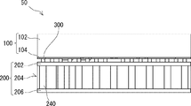
- FIG. 2 is a perspective view showing the structure of the quantum device 50 according to the first embodiment.
- FIG. 3 is an exploded view showing a laminated structure of the quantum device 50 according to the first embodiment.
- FIG. 4 is a schematic view of the quantum device 50 according to the first embodiment as viewed from the side.
- the quantum device 50 has a quantum chip 100 and an interposer 200.
- the quantum device 50 corresponds to the quantum device 1 shown in FIG.
- the quantum chip 100 corresponds to the quantum chip 10 shown in FIG.
- the interposer 200 corresponds to the interposer 20 shown in FIG.
- the quantum device 50 shown in FIGS. 2 to 4 corresponds to, for example, one qubit (1 bit).
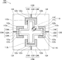
- FIG. 5 is a plan view showing the configuration of the quantum chip 100 (superconducting wiring layer 104) according to the first embodiment.
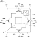
- FIG. 6 is a plan view showing the configuration of the interposer 200 (superconducting wiring layer 202) according to the first embodiment. Note that FIGS. 5 and 6 are views viewed from above in FIG. 2. Therefore, the configuration of FIG. 5 is superimposed on the configuration of FIG.
- the quantum chip 100 and the interposer 200 are shown separately in order to make the structure easier to understand, but in reality, both are connected as shown in FIG. Specifically, the quantum chip 100 and the interposer 200 are connected by a flip chip connection via a bump 300. As a result, the quantum chip 100 is flip-chip mounted on the interposer 200. That is, the quantum chip 100 faces the interposer 200 via the bump 300.
- the quantum chip 100 has a substrate 102 and a superconducting wiring layer 104.
- the superconducting wiring layer 104 is provided on the surface of the substrate 102 facing the interposer 200.
- the circuit of the resonator 110 and the coupler 122 is formed in the superconducting wiring layer 104.
- a ground electrode 124 (first ground electrode) is formed around the circuit of the resonator 110 and the coupler 122.
- the interposer 200 has a superconducting wiring layer 202, a substrate 204, and a superconducting wiring layer 206.
- the superconducting wiring layer 202 is provided on the surface of the substrate 204 on the side facing the quantum chip 100. Further, the superconducting wiring layer 206 is provided on the surface of the substrate 204 opposite to the quantum chip 100.
- the interposer 200 is configured to connect the quantum chip 100 and an external circuit (not shown). Further, as will be described later, the circuit of the magnetic field application circuit 212 and the reading unit 214 is formed in the superconducting wiring layer 202. Therefore, the interposer 200 can function as a quantum interposer. Further, a ground electrode 224 (second ground electrode) is formed on the superconducting wiring layer 202.
- the superconducting wiring layer 206 is formed with wiring connected to the superconducting wiring layer 202 via a through electrode 240 provided on the substrate 204.
- the superconducting wiring layer 206 is formed with wiring 212a and wiring 214a for connecting the magnetic field application circuit 212 and the readout unit 214 to an external circuit.
- the superconducting wiring layer 206 is provided with a ground electrode 250 (fourth ground electrode) around the wiring 212a and the wiring 214a.
- the through electrode 240 may be configured by being formed of a superconducting material. The through electrode 240 penetrates the substrate 204 and connects the ground electrode 224 and the ground electrode 250.
- the substrate 102 and the substrate 204 for example, a silicon substrate is used, but the material of the substrate is not limited to this.
- a sapphire substrate, a glass substrate, or the like may be used for the substrate 102 and the substrate 204.
- the superconducting wiring layers 104, 202, 206, the bump 300 and the through silicon via 240 are realized by the superconductor.
- Materials for superconductors include, for example, niobium, niobium nitride, aluminum, indium, lead, tin, rhenium, palladium, titanium, titanium nitride, tantalum, or alloys containing any of these.
- the superconducting wiring layers 104, 202, 206, bumps 300 and through silicon vias 240 may be realized by the superconductor, and at least a part of the superconducting wiring layer 104 except the superconducting wiring layer 104 may be a normal conductor. May be used. Materials for normal conductors include, for example, copper, silver, gold, platinum, or alloys containing any of these.
- the quantum device 50 is used in a temperature environment of, for example, about 10 mK (millikelvin) realized by a refrigerator.
- the circuit of the resonator 110 and the coupler 122 is formed in the superconducting wiring layer 104.
- the superconducting wiring layer 104 includes a conductive member 112 having a predetermined shape, a SQUID (superconducting quantum interference device) 116, a ground electrode 124, and a coupler 122.
- the conductive member 112 is formed in a cross shape.
- a ground electrode 124 is formed around the conductive member 112 and the coupler 122.
- a space G is provided between the conductive member 112 and the ground electrode 124.
- the conductive member 112 is capacitively coupled to the ground electrode 124 via the space G. That is, the space G constitutes the capacitor 118, which will be described later.
- a pair of Josephson joints 114A and 114B are provided between one end 112d of the conductive member 112 and the ground electrode 124a.
- the SQUID 116 is configured by a loop circuit formed by a pair of Josephson junctions 114A, 114B. That is, one end of the SQUID 116 is connected to the conductive member 112, and the other end is connected to the ground electrode 124a.
- the resonator 110 is composed of the conductive member 112 and the SQUID 116.
- Couplers 122A to 122D are provided in the vicinity of the four ends 112a to 112d of the conductive member 112, respectively.
- the coupler 122 is configured to couple adjacent qubits.
- the coupler 122 is a circuit for coupling to another resonator having the same configuration as the resonator 110.
- the coupler 122 may be capacitively coupled to the resonator 110 (conductive member 112).
- Each coupler 122 is formed in the vicinity of the ends 112a to 112d so as to surround each of the ends 112a to 112d of the conductive member 112.
- each coupler 122 has a discontinuous shape such as a branched portion 122a and a bent portion 122b. Due to such a shape, the coupler 122 surrounds each of the ends 112a to 112d of the conductive member 112.
- the coplanar line 120 is formed by the coupler 122 and the ground electrode 124 around the coupler 122.
- the coplanar line 120 is configured by providing a gap in the ground electrode 124 and forming a coupler 122 as a central conductor in the center of the gap. Therefore, the coplanar line 120 corresponds to the coplanar line 12 shown in FIG. 1, the coupler 122 corresponds to the center conductor 12a shown in FIG. 1, and the ground electrode 124 corresponds to the first ground electrode shown in FIG. Corresponds to 12b.
- the coplanar line 120 itself may function as a coupler. That is, the coplanar line 120 may correspond to the "coupler".
- a coupler 122A is provided in the vicinity of the end 112a of the conductive member 112 at a position moved 90 degrees counterclockwise from the end 112d provided with the Josephson junction 114 (SQUID 116).
- a coupler 122A is provided in the vicinity of the end 112a of the conductive member 112 at a position moved 90 degrees counterclockwise from the end 112d provided with the Josephson junction 114 (SQUID 116).
- a coupler 122A is provided in the vicinity of the end portion 112b at a position moved 90 degrees counterclockwise from the end portion 112a.
- a coplanar line 120B is formed by the coupler 122B and the ground electrode 124B around the coupler 122B.
- a coupler 122C is provided in the vicinity of the end portion 112c at a position moved 90 degrees counterclockwise from the end portion 112b.
- the coplanar line 120C is formed by the coupler 122C and the ground electrode 124C around the coupler 122C.
- a coupler 122D is provided in the vicinity of the end portion 112d.
- a coplanar line 120D is formed by the coupler 122D and the ground electrode 124D around the coupler 122D. That is, in the first embodiment, the coupler 122D (coplanar line 120D) is provided in the vicinity of the SQUID 116.
- a ground electrode 224 is formed in the superconducting wiring layer 202.
- a space A is provided at a position of the superconducting wiring layer 202 facing the resonator 110 and the coupler 122 of the superconducting wiring layer 104. That is, the ground electrode 224 is not formed in the region of the superconducting wiring layer 202 facing the resonator 110 and the coupler 122 of the superconducting wiring layer 104. This is because the characteristics of the qubit deteriorate when the resonator 110 and the coupler 122 are close to the ground electrode 224.
- the resonance frequency and Q value (Quality factor) of the resonator 110, the degree of coupling of the coupler 122, the characteristic impedance of the coplanar line 120, and the like are affected. Because there is.
- the ground electrode 224 is connected to the ground electrode 124 via a large number of bumps 300. That is, a plurality of bumps 300 are arranged between the ground electrode 124 and the ground electrode 224. Further, the plurality of bumps 300 are arranged in a grid pattern or randomly.
- the space A is provided with a magnetic field application circuit 212 and a readout unit 214.
- the magnetic field application circuit 212 is provided at a position facing the SQUID 116, and is magnetically coupled to the SQUID 116.
- the magnetic field application circuit 212 applies a magnetic field to the SQUID 116.
- the magnetic field is a DC magnetic field or an AC magnetic field.
- the resonator 110 and the magnetic field application circuit 212 constitute an oscillator 60, which will be described later. Therefore, it can be said that the quantum device 50 constitutes an oscillator 60 (qubit, qubit circuit).
- the magnetic field application circuit 212 is formed of electrodes and wiring having a predetermined shape. Specifically, as shown in FIGS. 2 and 6, the magnetic field application circuit 212 is composed of electrodes and wiring having a shape in which a part of the ring is missing, that is, a C-shape. That is, the magnetic field application circuit 212 is composed of substantially annular electrodes and wiring. When a current flows through the magnetic field application circuit 212, a magnetic field penetrating the inside of the current path along the substantially annular electrode or wiring is generated. Further, the magnetic field application circuit 212 may be magnetically coupled to the SQUID 116, and its shape does not have to be substantially annular.
- ground electrode 212b (third ground electrode) of the magnetic field application circuit 212 is connected to the ground electrode 124a via the bumps 300E and 300F. Further, the ground electrode 212b may be connected to the ground electrode as long as it is connected to the ground electrode 124a, and may be connected to the ground electrode 224 or the ground electrode 250.
- the reading unit 214 is provided at a position facing the conductive member 112, and is capacitively coupled to the conductive member 112.
- the reading unit 214 is an electrode for reading the internal state of the resonator 110 (oscillator 60), that is, the oscillating state.
- the reading unit 214 is connected to an external circuit (control unit) that acquires the internal state of the resonator 110 (oscillator 60) via the superconducting wiring layer 206 (wiring 214a).
- the shape of the reading unit 214 is, for example, a shape corresponding to the shape of the conductive member 112. In the present embodiment, the shape of the reading unit 214 is a cross shape.
- the reading unit 214 may be capacitively coupled to the conductive member 112, and the shape thereof does not have to be a cross shape.
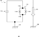
- FIG. 7 is a circuit diagram showing an oscillator 60 according to the first embodiment.
- FIG. 8 is a diagram showing an equivalent circuit of the oscillator 60 according to the first embodiment.
- the oscillator 60 has a resonator 110 and a magnetic field application circuit 212.
- the resonator 110 has a SQUID 116 and a capacitor 118.
- the SQUID 116 is shunted by the capacitor 118 via the conductive member 112.
- SQUID 116 is a circuit in which two Josephson junctions 114 (114A, 114B) are connected in a ring shape by a superconducting line. That is, the SQUID 116 is an annular loop circuit having two Josephson junctions 114 (114A, 114B).
- the Josephson junction refers to an element having a structure in which a thin insulating film is sandwiched between two superconductors. More specifically, as shown in FIG. 8, the SQUID 116 connects the first superconducting line 116a connecting the Josephson junction 114A and the Josephson junction 114B, and the Josephson junction 114A and the Josephson junction 114B. It is provided with a second superconducting line 116b.
- the resonator 110 includes SQUID 116, which is a loop circuit in which the first superconducting line 116a and the second superconducting line 116b are joined by a Josephson junction 114A and a Josephson junction 114B.
- a loop circuit (that is, SQUID 116) is configured by connecting the first superconducting line 116a and the Josephson junction 114A, the second superconducting line 116b and the Josephson junction 114B in an annular shape.
- the first superconducting line 116a and the second superconducting line 116b are joined by the Josephson junction 114A and the Josephson junction 114B to form a loop.
- a gap 222 is provided at a position of the superconducting wiring layer 202 facing the coupler 122. Specifically, a gap 222A is formed at a position facing the coupler 122A. Similarly, a gap 222B is formed at a position facing the coupler 122B. Further, a gap 222C is formed at a position facing the coupler 122C. Further, a gap 222D is formed at a position facing the coupler 122D.
- a gap 222E is provided at a position facing the coupler 122D and between the magnetic field application circuit 212 (ground electrode 212b) and the ground electrode 224.
- a space is formed in the region of the superconducting wiring layer 202 facing the coupler 122, but the configuration is not limited to this.
- the dielectric (board 204) may be exposed in the region facing the coupler 122 (the region where the ground electrode 224 is not formed). In this case, the gap 222 is formed so that the dielectric is exposed.
- a bridge-shaped bridge electrode 400 is provided in each gap 222. That is, the interposer 200 has a bridge electrode 400 formed so as to straddle the gap 222.
- the bridge electrode 400 is formed of a conductor (superconductor).
- the bridge electrode 400 corresponds to the connection electrode 40 shown in FIG. That is, the connection electrode 40 includes the bridge electrode 400 (first bridge electrode, second bridge electrode).
- the bridge electrode 400A (first bridge electrode) is provided in the gap 222A.
- the gap 222B is provided with a bridge electrode 400B (first bridge electrode).
- a bridge electrode 400C (first bridge electrode) is provided in the gap 222C.
- a bridge electrode 400D (first bridge electrode) is provided in the gap 222D.
- the gap 222E is provided with a bridge electrode 400E and a bridge electrode 400F (second bridge electrode).
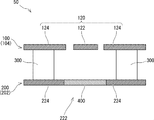
- FIG. 9 is a side view showing the structure around the gap 222 according to the first embodiment.
- the bridge electrode 400 is formed in a part of the gap 222.
- the bridge electrode 400 is formed in a bridge shape so as to partially connect the ground electrodes 224 around (both sides) the gap 222. In other words, the bridge electrode 400 partially connects the ground electrodes 224 around the gap 222. In other words, the bridge electrode 400 is formed so as to straddle the gap 222. Thereby, the potential difference of the potential (ground potential) of the ground electrode 224 around the gap 222 can be reduced.
- the bridge electrode 400 allows the potential (ground potential) of the ground electrode 224 around the gap 222 to be equipotential.
- FIG. 2 simply schematically shows the bridge electrode 400, and in reality, the bridge electrode 400 is formed in an arc shape. You don't have to. Rather, as shown in FIG. 9, the bridge electrode 400 is formed so as not to come into contact with the superconducting wiring layer 104 (coupler 122). That is, it is desirable that the bridge electrode 400 is formed as far as possible from the superconducting wiring layer 104 of the quantum chip 100 in order to suppress the deterioration of the characteristics of the quantum bit described above. Therefore, a part of the bridge electrode 400 (connection electrode) faces the coupler 122 (center conductor) via a space. Further, as shown in FIG.
- the bridge electrode 400 is formed in a linear shape. Further, as shown in FIG. 9, the bridge electrode 400 may be provided on the same plane as the ground electrode 224 (superconducting wiring layer 202). Further, the bridge electrode 400 may be integrally formed with the ground electrodes 224 (superconducting wiring layer 202) on both sides of the gap 222. By forming the bridge electrode 400 in this way, the bridge electrode 400 can be easily formed.
- the bump 300 may be provided in the vicinity of the bridge electrode 400.
- bumps 300A are provided on both sides of the bridge electrode 400A in the vicinity of the bridge electrode 400A.
- bumps 300B are provided on both sides of the bridge electrode 400B in the vicinity of the bridge electrode 400B.
- bumps 300C are provided on both sides thereof.
- bumps 300D are provided on both sides thereof.
- a bump 300D is provided at one end thereof, and a bump 300E is provided at a portion corresponding to the magnetic field application circuit 212 at the other end.
- a bump 300D is provided at one end thereof, and a bump 300F is provided at a portion corresponding to the magnetic field application circuit 212 at the other end.
- the bump 300 is connected to the ground electrode 224 and also to the ground electrode 124. Therefore, as shown in FIG. 9, the ground electrodes 124 on both sides of the coupler 122 corresponding to the center conductor in the coplanar line 120 are connected via the bump 300, the ground electrode 224, the bridge electrode 400, the ground electrode 224 and the bump 300. Will be done. Therefore, the bump 300, the ground electrode 224, the bridge electrode 400, the ground electrode 224, and the bump 300 form a U-shaped transmission line. This U-shaped transmission line functions as an air bridge connecting the ground electrodes 124 on both sides of the coupler 122.
- the ground electrode 124A around the coupler 122A is connected by the bump 300A, the ground electrode 224, the bridge electrode 400A, the ground electrode 224 and the bump 300A.
- the bump 300B, the ground electrode 224, the bridge electrode 400B, the ground electrode 224 and the bump 300B connect the ground electrode 124B around the coupler 122B.
- the ground electrode 124C around the coupler 122C is connected by the bump 300C, the ground electrode 224, the bridge electrode 400C, the ground electrode 224, and the bump 300C.
- the bump 300D, the ground electrode 224, the bridge electrode 400D, the ground electrode 224 and the bump 300D connect the ground electrode 124D around the coupler 122D.
- the ground electrode 124a and the ground electrode 124D around the coupler 122D are connected by the bump 300E, the ground electrode 212b of the magnetic field application circuit 212, the bridge electrode 400E, the ground electrode 224, and the bump 300D. Further, the ground electrode 124a and the ground electrode 124D around the coupler 122D are connected by the bump 300F, the ground electrode 212b of the magnetic field application circuit 212, the bridge electrode 400F, the ground electrode 224, and the bump 300D.
- FIG. 6 shows six bridge electrodes 400, the number of bridge electrodes 400 is not limited to six.
- the bridge electrode 400 may be formed so as to face the coupler 122, which is the central conductor of the coplanar line 120, and to straddle an arbitrary gap 222 provided with bumps 300 around the bridge electrode 400.
- the bump 300, the ground electrode 224, the bridge electrode 400, the ground electrode 224, and the bump 300 function as an air bridge connecting the ground electrodes 124 on both sides of the coupler 122.
- the potential difference between the ground electrodes 124 on both sides of the coupler 122 can be reduced.
- the potential difference between the ground electrodes 124 on both sides of the coupler 122 can be set to zero.
- an energy leakage mode such as a slot line mode or a Coupled Slotline Mode, which is an undesired mode. That is, it is possible to prevent the electromagnetic field distribution in the width direction (horizontal direction in FIG.
- an air bridge straddling the waveguide may be formed in order to suppress the occurrence of an energy leakage mode such as a slot line mode.
- an energy leakage mode such as a slot line mode.
- the quantum chip 100 and the interposer 200 are flip-chip mounted, it is not preferable to provide an air bridge from the viewpoint of technology and space.
- the first embodiment since the same function as the air bridge can be realized without providing the air bridge, the occurrence of the energy leakage mode can be suppressed. Therefore, in the quantum device 50 according to the first embodiment, it is possible to suppress the deterioration of the performance of the qubit even when the flip chip is mounted.
- bridge electrodes 400 are formed in one gap 222 because the characteristics of the qubit deteriorate when the coupler 122 is close to the ground electrode 224.
- the number of bridge electrodes 400 can be appropriately set depending on, for example, design conditions.
- the bridge electrode 400 is not provided at a position facing the resonator 110 (conductive member 112 and SQUID 116). As a result, deterioration of the performance of the qubit (resonator 110) can be suppressed. For example, by providing the bridge electrode 400 at a position not facing the resonator 110 (conductive member 112 and SQUID 116), deterioration of coherence can be suppressed.
- the coherence is, for example, the coherence time, which is the time during which the oscillator 60 functions as a qubit.
- the bridge electrode 400 is provided at a position corresponding to the discontinuous shape of the coupler 122.
- the bridge electrode 400A is formed in the vicinity of the branch portion 122a of the coupler 122A.
- the bridge electrode 400B is formed in the vicinity of the branch portion 122a of the coupler 122B.
- the bridge electrode 400C is formed in the vicinity of the branch portion 122a of the coupler 122C.
- the bridge electrode 400D is formed in the vicinity of the branch portion 122a of the coupler 122D.
- the bridge electrodes 400E and 400F are formed in the vicinity of the branch portion 122a and the bent portion 122b of the coupler 122D.
- a gap 222E is provided between the ground electrode 212b and the ground electrode 224 of the magnetic field application circuit 212 at a position facing the coupler 122D (center conductor) in the vicinity of the SQUID 116. Then, the bridge electrode 400E and the bridge electrode 400F are formed so as to straddle the gap 222E. Then, the ground electrode 212b and the ground electrode 224 are partially connected by these bridge electrodes 400E and 400F. Further, one end of the bridge electrodes 400E and 400F is located near the bumps 300E and 300F connected to the ground electrode 124 and the ground electrode 212b, and the other end of the bump 300 connected to the ground electrode 124 and the ground electrode 224. It is located in the vicinity.
- the ground electrodes around the coupler 122D are connected by three bridge electrodes 400D, 400E, and 400F. Further, the three bridge electrodes 400D, 400E and 400F are formed in the vicinity of the branch portion 122a of the coupler 122D. Therefore, it is possible to more effectively suppress the occurrence of the energy leakage mode. It should be noted that this configuration can also be applied to other embodiments described later.
- a plurality of bumps 300 are arranged in a grid pattern or randomly between the ground electrode 124 and the ground electrode 224. This increases the possibility that the bump 300 will be placed in the vicinity of the bridge electrode 400. Further, by arranging the bumps 300 in this way, the ground electrode 124 and the ground electrode 224 are more reliably connected.
- FIG. 10 is a diagram showing the configuration of the quantum device 50 according to the second embodiment.
- FIG. 10 is a perspective view showing the quantum device 50 according to the second embodiment.
- FIG. 10 corresponds to FIG. 2 according to the first embodiment.
- the quantum device 50 has a quantum chip 100 and an interposer 200. Since the configuration of the quantum chip 100 is substantially the same as that of the first embodiment, the description thereof will be omitted. Further, the configuration of the interposer 200 is substantially the same as that of the first embodiment except for the bridge electrode 400, and thus the description thereof will be omitted. Please refer to FIG. 2 for the positions of the gaps 222 (222A to 222D).
- the interposer 200 has an outer frame structure 420 of a conductor (superconductor) formed so as to surround the superconducting wiring layer 202 of the interposer 200.
- the outer frame structure 420 is integrally formed with the ground electrode 224.
- the outer frame structure 420 has an outer frame portion 422A corresponding to the gap 222A, an outer frame portion 422B corresponding to the gap 222B, an outer frame portion 422C corresponding to the gap 222C, and an outer frame portion 422D corresponding to the gap 222D. That is, the outer frame portion 422 is provided at a position corresponding to each gap 222 of the outer frame structure 420.
- the outer frame portion 422 connects the ground electrodes 224 around the gap 222 (both ends). That is, the outer frame portion 422 corresponds to the connection electrode 40 shown in FIG. In other words, the connection electrode 40 includes an outer frame portion 422. In other words, the outer frame portion 422 functions as the connection electrode 40 shown in FIG. Therefore, the bump 300 formed in the vicinity of the outer frame portion 422 is connected to the ground electrode 124 and the ground electrode 224.
- bumps 300A are provided on both sides of the outer frame portion 422A in the vicinity of the outer frame portion 422A.
- bumps 300B are provided on both sides of the outer frame portion 422B in the vicinity of the outer frame portion 422B.
- bumps 300C are provided on both sides thereof.
- bumps 300D are provided on both sides thereof.
- the ground electrodes 124 on both sides of the coupler 122 corresponding to the central conductor in the coplanar line 120 are the bump 300, the ground electrode 224, the outer frame portion 422, and the ground electrode. It will be connected via the 224 and the bump 300.
- the bump 300, the ground electrode 224, the outer frame portion 422, the ground electrode 224, and the bump 300 form a U-shaped transmission path. This U-shaped transmission line functions as an air bridge connecting the ground electrodes 124 on both sides of the coupler 122.
- the bump 300A, the ground electrode 224, the outer frame portion 422A, the ground electrode 224, and the bump 300A connect the ground electrode 124A around the coupler 122A.
- the bump 300B, the ground electrode 224, the outer frame portion 422B, the ground electrode 224, and the bump 300B connect the ground electrode 124B around the coupler 122B.
- the ground electrode 124C around the coupler 122C is connected by the bump 300C, the ground electrode 224, the outer frame portion 422C, the ground electrode 224, and the bump 300C.
- the ground electrode 124D around the coupler 122D is connected by the bump 300D, the ground electrode 224, the outer frame portion 422D, the ground electrode 224, and the bump 300D.
- the bump 300, the ground electrode 224, the outer frame portion 422, the ground electrode 224, and the bump 300 function as an air bridge connecting the ground electrodes 124 on both sides of the coupler 122. Therefore, as in the second embodiment, the same effect as that of the first embodiment can be obtained by providing the outer frame structure 420 of the conductor formed so as to surround the superconducting wiring layer 202 of the interposer 200 and integrated with the ground electrode 224. Can be played. That is, also in the second embodiment, the potential difference between the ground electrodes 124 on both sides of the coupler 122 can be reduced. Preferably, the potential difference between the ground electrodes 124 on both sides of the coupler 122 can be set to zero. Therefore, even with the configuration according to the second embodiment, it is possible to suppress the occurrence of the energy leakage mode in the coupler 122.
- the outer peripheral portion of the interposer 200 has a high degree of freedom in wiring because it is unlikely that the wiring necessary for realizing the qubit will be arranged. Therefore, even if the ground electrode is arranged on the outer peripheral portion of the interposer 200, it is extremely unlikely that it will affect the overall arrangement. Therefore, by providing the outer frame structure 420, it becomes possible to easily form the outer frame portion 422 having substantially the same function as the bridge electrode 400 according to the first embodiment. That is, the connection electrode 40 can be easily arranged as compared with the configuration according to the first embodiment.
- FIG. 11 is a diagram showing the configuration of the quantum device 50 according to the third embodiment.
- FIG. 11 is a perspective view showing the quantum device 50 according to the third embodiment.
- FIG. 11 corresponds to FIG. 2 according to the first embodiment.
- the quantum device 50 has a quantum chip 100 and an interposer 200. Since the configuration of the quantum chip 100 is substantially the same as that of the first embodiment, the description thereof will be omitted. Further, the configuration of the interposer 200 is substantially the same as that of the first embodiment except for the bridge electrode 400, and thus the description thereof will be omitted. Please refer to FIG. 2 for the positions of the gaps 222 (222A to 222D).
- FIG. 12 is a side view showing the structure around the gap 222 according to the third embodiment.
- the through electrode 240 is provided in the vicinity of the gap 222.
- the through electrode 240 and the ground electrode 250 (fourth ground electrode) connect the ground electrodes 224 around the gap 222 (both sides). Therefore, the through electrode 240 and the ground electrode 250 correspond to the connection electrode 40 shown in FIG.
- the through electrode 240 and the ground electrode 250 constitute the connection electrode 440.
- the through electrode 240 and the ground electrode 250 function as the connection electrode 440.
- the connecting electrode 440 includes a configuration made up of a through electrode 240 and a ground electrode 250. With such a configuration, a part of the connection electrode 440 (a part of the ground electrode 250) faces the coupler 122 (center conductor) via a space.
- through electrodes 240A are formed in the vicinity of both sides of the gap 222A. Then, the ground electrode 224 around the gap 222A is connected by the connection electrode 440A composed of the through electrode 240A and the ground electrode 250A.
- through electrodes 240B are formed in the vicinity of both sides of the gap 222B. Then, the ground electrode 224 around the gap 222B is connected by the connection electrode 440B composed of the through electrode 240B and the ground electrode 250B.
- through electrodes 240C are formed in the vicinity of both sides of the gap 222C. Then, the ground electrode 224 around the gap 222C is connected by the connection electrode 440C composed of the through electrode 240C and the ground electrode 250C.
- through electrodes 240D are formed in the vicinity of both sides of the gap 222D. Then, the ground electrode 224 around the gap 222D is connected by the connection electrode 440D composed of the through electrode 240D and the ground electrode 250D.
- the bump 300 is connected to the ground electrode 224 and also to the ground electrode 124. Therefore, as shown in FIG. 12, the ground electrodes 124 on both sides of the coupler 122 are connected via the bump 300, the ground electrode 224, the through electrode 240, the ground electrode 250, the through electrode 240, the ground electrode 224, and the bump 300.
- the Rukoto Therefore, the bump 300, the ground electrode 224, the through electrode 240, the ground electrode 250, the through electrode 240, the ground electrode 224, and the bump 300 form a U-shaped transmission path. This U-shaped transmission line functions as an air bridge connecting the ground electrodes 124 on both sides of the coupler 122.
- the ground electrode 124A around the coupler 122A is connected by the bump 300A, the ground electrode 224, the through electrode 240A, the ground electrode 250A, the through electrode 240A, the ground electrode 224 and the bump 300A.
- the bump 300B, the ground electrode 224, the through electrode 240B, the ground electrode 250B, the through electrode 240B, the ground electrode 224 and the bump 300B connect the ground electrode 124B around the coupler 122B.
- the ground electrode 124C around the coupler 122C is connected by the bump 300C, the ground electrode 224, the through electrode 240C, the ground electrode 250C, the through electrode 240C, the ground electrode 224 and the bump 300C.
- the ground electrode 124D around the coupler 122D is connected by the bump 300D, the ground electrode 224, the through electrode 240D, the ground electrode 250D, the through electrode 240D, the ground electrode 224 and the bump 300D.
- the bump 300, the ground electrode 224, the through electrode 240, the ground electrode 250, the through electrode 240, the ground electrode 224, and the bump 300 connect the ground electrodes 124 on both sides of the coupler 122. Acts as a bridge. Therefore, even in the third embodiment, the same effect as that of the first embodiment can be obtained. That is, also in the third embodiment, the potential difference between the ground electrodes 124 on both sides of the coupler 122 can be reduced. Preferably, the potential difference between the ground electrodes 124 on both sides of the coupler 122 can be set to zero. Therefore, even with the configuration according to the third embodiment, it is possible to suppress the occurrence of the energy leakage mode in the coupler 122.
- the potential difference between the ground electrodes 124 on both sides of the coupler 122 can be reduced without forming a structure such as a bridge electrode that straddles the gap 222. Therefore, in the configuration according to the third embodiment, the structure can be simplified as compared with the configurations according to the first embodiment and the second embodiment.
- the thickness of the substrate 204 is sufficiently thin in order to shorten the length of the through electrode 240.
- the length of the through electrode 240 is relative to the wavelength (operating wavelength) of the signal used to realize the operation of the qubit (the signal used to realize the operation of the oscillator 60 (high frequency signal; electromagnetic wave)). It is desirable that it is short enough.
- the length of the through electrode 240 is preferably 1/20 or less of the operating wavelength.
- the length of the through electrode 240 may be such that the path composed of the bump 300, the bridge electrode 400, and the ground electrode 224 may be replaced with the path composed of the bump 300, the through electrode 240, and the ground electrode 250. It can be said that the distance is short enough.
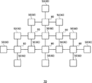
- FIG. 13 is a diagram showing a configuration of a quantum computer 70 composed of a plurality of quantum devices 50 according to the above-described embodiment.
- the quantum computer 70 is, for example, a quantum annealing type computer that calculates the solution of an arbitrary problem that can be mapped to the Ising model.
- the oscillator 60 composed of the quantum device 50 oscillates parametrically and realizes a qubit (quantum bit circuit).
- the quantum computer 70 has a plurality of quantum devices 50 and at least one coupling circuit 80.
- the coupling circuit 80 is a circuit that couples a plurality of oscillators 60 (qubits, qubit circuits) composed of a plurality of quantum devices 50.
- the coupling circuit 80 is a circuit that couples a plurality of quantum devices 50.
- the quantum computer 70 is a computer in which a plurality of oscillators 60 composed of a plurality of quantum devices 50 form a network via a coupling circuit 80.
- the quantum computer 70 is configured by arranging a plurality of quantum devices 50 in an array via a coupling circuit 80.
- the coupling circuit 80 couples four quantum devices 50 (oscillator 60).
- the coupling circuit 80 is coupled to the four oscillators 60.
- the coupling circuit 80 includes the coupler 122 described above.
- the coupler 122 described above is a terminal of the coupling circuit 80 for coupling with the resonator 110 (oscillator 60). Therefore, the coupling circuit 80 couples between a plurality of qubits composed of the plurality of quantum devices 50, and includes a coupler 122.
- the coupling circuit 80 is connected to four quantum devices 50 (oscillator 60), but the number of quantum devices 50 (oscillator 60) to which one coupling circuit 80 can be coupled is designed. It can be set as appropriate depending on the conditions.
- the quantum device 50 according to the present embodiment is configured as described above, it is possible to suppress the occurrence of the energy leakage mode in the coupler 122. Therefore, it is possible to suppress the deterioration of the performance of the qubit. Since the quantum computer 70 according to the present embodiment is composed of such a quantum device 50, the performance of the entire qubit can be improved.
- the coupler 122 is provided in the vicinity of all four ends 112a to 112d of the conductive member 112.
- the coupler 122 does not have to be provided in the vicinity of all four ends 112a to 112d of the conductive member 112.
- the coupler 122 may be appropriately arranged depending on the arrangement of the quantum device 50 (oscillator 60) in the quantum computer.
- the resonator 110 is configured such that the conductive member 112 has a cross shape and the SQUID 116 is provided at the end of the cross shape.
- the configuration of the resonator 110 is not limited to such a configuration.
- the connection electrode 40 (bridge electrode 400, etc.) according to the present embodiment is applicable regardless of the position of the SQUID 116 and the shape of the conductive member 112.
- a modified example with respect to the first embodiment is shown, but the same applies to the other embodiments.
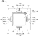
- FIG. 14 is a plan view showing the configuration of the quantum chip 100 (superconducting wiring layer 104) according to the first modification.
- FIG. 15 is a plan view showing the configuration of the interposer 200 (superconducting wiring layer 202) according to the first modification.
- the position of the SQUID 116 is different from the above-described embodiment.
- one end of the SQUID 116 is connected to the constricted portion of the cross-shaped conductive member 112, and the other end is connected to the ground electrode 124.
- the resonator 110 is composed of the conductive member 112 and the SQUID 116.
- the four couplers 122 are arranged on the four sides of the conductive member 112. Specifically, couplers 122 (122A to 122D) are provided in the vicinity of each of the four ends 112a to 112d of the conductive member 112. Further, as in the above-described embodiment, the coplanar line 120 is formed by the coupler 122 and the ground electrode 124 around the coupler 122.
- the position of the magnetic field application circuit 212 that applies a magnetic field to the SQUID 116 is also different from the above-described embodiment. That is, as shown in FIG. 15, the magnetic field application circuit 212 is arranged at a position of the superconducting wiring layer 202 facing the SQUID 116 shown in FIG. Further, as in the above-described embodiment, the cross-shaped reading portion 214 is arranged at a position of the superconducting wiring layer 202 facing the conductive member 112.
- a gap 222 is formed at a position facing each coplanar line 120 of the superconducting wiring layer 202.
- a bridge electrode 400 is provided so as to straddle each gap 222.
- the bump 300 may be provided in the vicinity of the bridge electrode 400. Therefore, the ground electrodes 124 on both sides of the coupler 122 are connected via the bump 300, the ground electrode 224, the bridge electrode 400, the ground electrode 224, and the bump 300. As a result, the potential difference between the ground electrodes 124 on both sides of the coupler 122 can be reduced. Therefore, also in the first modification, it is possible to suppress energy leakage between the ground electrodes 124 across the central conductor, as in the above-described embodiment.
- FIG. 16 is a plan view showing the configuration of the quantum chip 100 (superconducting wiring layer 104) according to the second modification.
- FIG. 17 is a plan view showing the configuration of the interposer 200 (superconducting wiring layer 202) according to the second modification.
- the shape of the conductive member constituting the resonator 110 is different from that of the above-described embodiment.
- a quadrangular (for example, a square) conductive member 112A is used instead of the cross-shaped conductive member 112. Further, one end of the SQUID 116 is connected to one corner of the conductive member 112A, and the other end is connected to the ground electrode 124.
- the resonator 110 is composed of the conductive member 112A and the SQUID 116.
- couplers 122 are arranged on all sides of the conductive member 112A. Specifically, couplers 122 (122A to 122D) are provided in the vicinity of each of the four sides of the conductive member 112A. Further, as in the above-described embodiment, the coplanar line 120 is formed by the coupler 122 and the ground electrode 124 around the coupler 122.
- the position of the magnetic field application circuit 212 that applies a magnetic field to the SQUID 116 is also different from the above-described embodiment. That is, as shown in FIG. 17, the magnetic field application circuit 212 is arranged at a position of the superconducting wiring layer 202 facing the SQUID 116 shown in FIG. Further, a quadrangular (for example, square) reading unit 214A is arranged at a position of the superconducting wiring layer 202 facing the conductive member 112A.
- a gap 222 is formed at a position facing each coplanar line 120 of the superconducting wiring layer 202.
- a bridge electrode 400 is provided so as to straddle each gap 222.
- the bump 300 may be provided in the vicinity of the bridge electrode 400. Therefore, the ground electrodes 124 on both sides of the coupler 122 are connected via the bump 300, the ground electrode 224, the bridge electrode 400, the ground electrode 224, and the bump 300. As a result, the potential difference between the ground electrodes 124 on both sides of the coupler 122 can be reduced. Therefore, also in the second modification, it is possible to suppress energy leakage between the ground electrodes 124 across the central conductor, as in the above-described embodiment.
- FIG. 18 is a plan view showing the configuration of the quantum chip 100 (superconducting wiring layer 104) according to the third modification.
- FIG. 19 is a plan view showing the configuration of the interposer 200 (superconducting wiring layer 202) according to the third modification.
- the shape of the conductive member constituting the resonator 110 is different from that of the above-described embodiment.
- a circular conductive member 112B is used instead of the cross-shaped conductive member 112. Further, one end of the SQUID 116 is connected to the conductive member 112B, and the other end is connected to the ground electrode 124.
- the resonator 110 is composed of the conductive member 112B and the SQUID 116.
- couplers 122 are arranged on all sides of the conductive member 112B. Specifically, couplers 122 (122A to 122D) are provided in the vicinity of each of the four sides of the conductive member 112B. Further, as in the above-described embodiment, the coplanar line 120 is formed by the coupler 122 and the ground electrode 124 around the coupler 122.
- the position of the magnetic field application circuit 212 that applies a magnetic field to the SQUID 116 is also different from the above-described embodiment. That is, as shown in FIG. 19, the magnetic field application circuit 212 is arranged at a position of the superconducting wiring layer 202 facing the SQUID 116 shown in FIG. Further, the circular reading portion 214B is arranged at a position of the superconducting wiring layer 202 facing the conductive member 112B.
- a gap 222 is formed at a position facing each coplanar line 120 of the superconducting wiring layer 202.
- a bridge electrode 400 is provided so as to straddle each gap 222.
- the bump 300 may be provided in the vicinity of the bridge electrode 400. Therefore, the ground electrodes 124 on both sides of the coupler 122 are connected via the bump 300, the ground electrode 224, the bridge electrode 400, the ground electrode 224, and the bump 300. As a result, the potential difference between the ground electrodes 124 on both sides of the coupler 122 can be reduced. Therefore, also in the third modification, it is possible to suppress energy leakage between the ground electrodes 124 across the central conductor, as in the above-described embodiment.
- (Appendix 1) The quantum chips that make up the qubit and An interposer facing the quantum chip and having a conductor formed at least on the surface facing the quantum chip.
- the quantum chip is flip-chip mounted on the interposer by bumps.
- a coplanar line for coupling between adjacent qubits is formed on the quantum chip, and the coplanar line is composed of a center conductor and a first ground electrode around the center conductor.
- the conductor is not partially formed along the path of the coplanar line at a position facing the central conductor of the coplanar line, and the conductor is formed.
- a second ground electrode is formed around the gap that is not formed.
- the interposer has a connecting electrode connecting the second ground electrode around the gap.
- the bump formed in the vicinity of the connection electrode is connected to the first ground electrode and the second ground electrode.
- Quantum device. (Appendix 2)
- the quantum chip is provided with a resonator.
- the connection electrode is formed at a position not facing the resonator of the interposer.
- the quantum device according to Appendix 1. (Appendix 3)
- the resonator has a conductive member having a predetermined shape and has a predetermined shape.
- the central conductor is provided in the vicinity of the conductive member.
- the quantum device according to Appendix 2. (Appendix 4)
- the connection electrode includes a bridge-shaped first bridge electrode formed so as to straddle a part of the gap.
- the bump formed in the vicinity of the first bridge electrode is connected to the first ground electrode and the second ground electrode.
- the quantum device according to any one of Supplementary note 1 to 3. (Appendix 5)
- the central conductor has a discontinuous shape and has a discontinuous shape.
- the first bridge electrode is provided at a position corresponding to the discontinuous shape in the gap.
- the quantum device according to Appendix 4. (Appendix 6)
- the first bridge electrode is formed on the same plane as the second ground electrode around the gap.
- the quantum chip is provided with a resonator.
- the resonator has a SQUID (superconducting quantum interference device) and has.
- the central conductor is provided in the vicinity of the SQUID.
- the interposer is provided with a magnetic field application circuit that applies a magnetic field to the SQUID.
- a gap is provided between the third ground electrode and the second ground electrode of the magnetic field application circuit at a position facing the central conductor in the vicinity of the SQUID.
- the interposer has a bridge-shaped second bridge electrode formed so as to straddle a part of the gap.
- the third ground electrode and the second ground electrode are partially connected by the second bridge electrode.
- the quantum device according to any one of Supplementary note 1 to 6. (Appendix 8) One end of the second bridge electrode is located near the first ground electrode and the bump connected to the third ground electrode, and the other end of the second bridge electrode is the first ground electrode.
- the quantum device according to Appendix 7 Located in the vicinity of the bump connected to the ground electrode and the second ground electrode, The quantum device according to Appendix 7. (Appendix 9)
- the interposer has an outer frame structure of a conductor formed so as to surround a superconducting wiring layer facing the quantum chip of the interposer and integrally formed with the second ground electrode.
- the outer frame portion of the outer frame structure provided at the position corresponding to the gap functions as the connection electrode.
- the quantum device according to Appendix 1. (Appendix 10)
- a fourth ground electrode is formed on the surface of the interposer opposite to the surface facing the qubit.
- a through electrode formed between the second ground electrode and the fourth ground electrode so as to connect the second ground electrode and the fourth ground electrode and penetrate the substrate of the interposer.
- the connection electrode is configured by the through electrode in the vicinity of the gap and the fourth ground electrode.
- the quantum device according to Appendix 1. (Appendix 11) The length of the through silicon via is less than or equal to a predetermined value with respect to the wavelength of the signal operating to realize the qubit.
- the quantum device according to Appendix 10. (Appendix 12) The length of the through electrode is 1/20 or less of the wavelength.
- the quantum device according to Appendix 11. Appendix 13) A plurality of the bumps are arranged in a grid pattern or randomly between the first ground electrode and the second ground electrode.
- a second ground electrode is formed in a region facing the first ground electrode.
- the interposer has a connecting electrode connected to the second ground electrode.
- the bump formed in the vicinity of the connection electrode is connected to the first ground electrode and the second ground electrode. At least a part of the connection electrode faces the center conductor via a space. Quantum device.
- Quantum device 10
- Quantum chip 12
- First ground electrode 20
- Interposer 22 Gap 24
- Second ground electrode 30
- Bump 40 Connection electrode 50
- Quantum device 60
- Oscillator 70
- Quantum computer 80
- Coupling circuit 100
- Quantum chip 102
- Substrate 104
- Superconducting wiring layer 110
- Resonator 112
- Conductive member 114
- Josephson junction 118
- Capsule 120
- Ground electrode 200
- Interposer 202
- Superconducting wiring layer 204
- Board 206
- Superconducting wiring layer 212
- Magnetic field application circuit 214 Read Part 222 Gap 224
- Ground electrode 240
- Penetration electrode 250
- Ground electrode 300 Bump 400
- Bridge electrode 420
- Outer frame part 440 Connection electrode
Landscapes
- Engineering & Computer Science (AREA)
- Physics & Mathematics (AREA)
- General Physics & Mathematics (AREA)
- Theoretical Computer Science (AREA)
- Condensed Matter Physics & Semiconductors (AREA)
- Mathematical Analysis (AREA)
- Evolutionary Computation (AREA)
- Data Mining & Analysis (AREA)
- Computational Mathematics (AREA)
- Mathematical Optimization (AREA)
- Pure & Applied Mathematics (AREA)
- Computing Systems (AREA)
- General Engineering & Computer Science (AREA)
- Mathematical Physics (AREA)
- Software Systems (AREA)
- Artificial Intelligence (AREA)
- Superconductor Devices And Manufacturing Methods Thereof (AREA)
Abstract
量子チップをインターポーザにフリップチップ実装する場合でも量子ビットの性能の低下を抑制することが可能な量子デバイスを提供する。量子チップ(10)は、インターポーザ(20)に、バンプ(30)によってフリップチップ実装されている。量子チップ(10)には、隣り合う量子ビット間を結合するコプレーナ線路12が形成されている。インターポーザ(20)において、コプレーナ線路(12)の中心導体(12a)と対向する箇所には、隙間(22)が設けられている。隙間(22)の周囲には、第2のグランド電極(24)が形成されている。インターポーザ(20)は、隙間(22)の周囲の第2のグランド電極(24)を接続する接続電極(40)を有する。接続電極(40)の近傍に形成されたバンプ(30A)は、第1のグランド電極(12b)及び第2のグランド電極(24)と接続されている。
Description
本発明は、量子デバイス及び量子計算機に関する。
特許文献1は、電子回路、電子回路と磁場印加部とを備える発振器、及び、発振器とカプラとを備えた計算装置(量子計算機)を開示する。また、特許文献2は、細長い薄膜と、超伝導量子干渉デバイス(SQUID)と、接地面とを備える量子ビットデバイスを開示する。SQUIDは、細長い薄膜の近位端と電気接触し、3つより少ないジョセフソン接合を有する。接地面は、細長い薄膜と同一平面内にあり、細長い薄膜の遠位端と電気接触している。
接地面を同一の電圧に保つことによってコプレーナ線路からの望ましくない伝送動作であるスロットラインモードを抑制するために、デバイス上にエアブリッジを形成することが知られている。特許文献2では、導波管からの望ましくないスロットラインモード等を抑制するのを支援するために、デバイス上にクロスオーバエアブリッジが製作される。一方で、多数のマイクロ波信号を送受する配線の複雑さを緩和し、かつ配置スペースを節約するため、量子ビット(共振器)を構成する量子チップを、インターポーザに、バンプを用いてフリップチップ実装することがある。ここで、特許文献2に記載されたエアブリッジを設けた量子チップをインターポーザにフリップチップ実装(フリップチップ接続)する場合、フリップチップ実装に伴うプロセスに起因して、エアブリッジが変形又は破壊するおそれがある。したがって、エアブリッジを用いて接地面を同一の電圧に保つことが困難となるので、スロットラインモード等のエネルギー漏洩モードが十分に抑制されず、量子ビットの性能が低下するおそれがある。
本開示の目的は、このような課題を解決するためになされたものであり、量子チップをインターポーザにフリップチップ実装する場合でも量子ビットの性能の低下を抑制することが可能な量子デバイス及び量子計算機を提供することにある。
本開示にかかる量子デバイスは、量子ビットを構成する量子チップと、前記量子チップと対向し、少なくとも前記量子チップと対向する面には導電体が形成されているインターポーザと、を有し、前記量子チップは、前記インターポーザにバンプによってフリップチップ実装され、前記量子チップには、隣り合う量子ビット間を結合するためのコプレーナ線路が形成され、前記コプレーナ線路は、中心導体と、前記中心導体の周囲の第1のグランド電極とで構成され、前記インターポーザの前記量子チップと対向する面において、前記コプレーナ線路の前記中心導体と対向する箇所では、前記コプレーナ線路の経路に沿って部分的に前記導電体が形成されておらず、前記導電体が形成されていない隙間の周囲には、第2のグランド電極が形成されており、前記インターポーザは、前記隙間の周囲の前記第2のグランド電極を接続する接続電極を有し、前記接続電極の近傍に形成された前記バンプは、前記第1のグランド電極及び前記第2のグランド電極と接続されている。
また、本開示にかかる別の量子デバイスは、量子ビットを構成する量子チップと、前記量子チップと対向して設けられたインターポーザと、を有し、前記量子チップは、前記インターポーザにバンプによってフリップチップ実装され、前記量子チップには、隣り合う量子ビット間を結合するためのコプレーナ線路が形成され、前記コプレーナ線路は、中心導体と、前記中心導体の周囲の第1のグランド電極とで構成され、前記インターポーザには、前記第1のグランド電極と対向する領域に第2のグランド電極が形成されており、前記インターポーザは、前記第2のグランド電極に接続する接続電極を有し、前記接続電極の近傍に形成された前記バンプは、前記第1のグランド電極及び前記第2のグランド電極と接続され、少なくとも前記接続電極の一部が、前記中心導体と空間を介して対向している。
また、本開示にかかる別の量子デバイスは、量子ビットを構成する量子チップと、前記量子チップと対向して設けられたインターポーザと、を有し、前記量子チップは、前記インターポーザにバンプによってフリップチップ実装され、前記量子チップには、隣り合う量子ビット間を結合するためのコプレーナ線路が形成され、前記コプレーナ線路は、中心導体と、前記中心導体の周囲の第1のグランド電極とで構成され、前記インターポーザには、前記第1のグランド電極と対向する領域に第2のグランド電極が形成されており、前記インターポーザは、前記第2のグランド電極に接続する接続電極を有し、前記接続電極の近傍に形成された前記バンプは、前記第1のグランド電極及び前記第2のグランド電極と接続され、少なくとも前記接続電極の一部が、前記中心導体と空間を介して対向している。
また、本開示にかかる量子計算機は、複数の前記量子デバイスと、複数の前記量子デバイスで構成される複数の前記量子ビット間を結合し、前記中心導体で構成されるカプラを含む、少なくとも1つの結合回路と、を有する。
本開示によれば、量子チップをインターポーザにフリップチップ実装する場合でも量子ビットの性能の低下を抑制することが可能な量子デバイス及び量子計算機を提供できる。
(本開示にかかる実施の形態の概要)
本開示の実施形態の説明に先立って、本開示にかかる実施の形態の概要について説明する。図1は、本実施の形態にかかる量子デバイス1の概要を示す図である。
本開示の実施形態の説明に先立って、本開示にかかる実施の形態の概要について説明する。図1は、本実施の形態にかかる量子デバイス1の概要を示す図である。
量子デバイス1は、量子ビット(量子ビット回路,発振器)を構成する量子チップ10と、量子チップ10と対向するインターポーザ20とを有する。インターポーザ20の少なくとも量子チップ10に対向する面20aには、導電体が形成されている。導電体は、超伝導材料であってもよいし、常伝導材料であってもよい。また、導電体は、グランド電極、配線、又はパッド等を含み得る。また、量子チップ10は、インターポーザ20に、バンプ30によってフリップチップ実装されている。なお、例えば、量子デバイス1は、量子ビットの1ビットに相当するデバイスである。そして、複数の量子デバイス1または量子チップ10が配列することで、量子計算機が構成される。
また、量子チップ10には、隣り合う量子ビット間を結合するコプレーナ線路12が形成されている。ここで、コプレーナ線路12は、中心導体12aと、中心導体12aの周囲(両側)の第1のグランド電極12bとで構成されている。また、インターポーザ20において、コプレーナ線路12の中心導体12aと対向する箇所には、隙間22が設けられている。つまり、インターポーザ20の量子チップ10と対向する面において、コプレーナ線路12の中心導体12aと対向する箇所では、コプレーナ線路12の経路に沿って部分的に導電体が形成されていない。この、導電体が形成されていない隙間22では、誘電体が露出していてもよい。そして、インターポーザ20の隙間22の周囲(両側)には、第2のグランド電極24が形成されている。つまり、導電体が形成されていない箇所の周囲には、第2のグランド電極24が形成されている。つまり、インターポーザ20の面20aに形成された導電体は、第1のグランド電極12bと対向する領域に、第2のグランド電極24を有する。
また、インターポーザ20は、隙間22の周囲の第2のグランド電極24を接続する接続電極40を有する。つまり、接続電極40の両端は、第2のグランド電極24と接続されている。例えば、隙間22の一部には、隙間22の周囲の第2のグランド電極24を部分的に接続する橋梁状の接続電極40(橋梁電極)が形成されている。例えば、誘電体が露出した領域である隙間22の一部に、接続電極40が設けられていてもよい。つまり、導電体が形成されていない箇所には、当該箇所の周囲の第2のグランド電極24を接続する接続電極40が形成されている。言い換えると、接続電極40の少なくとも一部は、中心導体12aと対向する領域の一部と重なる位置に設けられている。なお、図1では、接続電極40は直線状に形成されているが、接続電極40は、このような形状に限られない。そして、接続電極40の近傍に形成されたバンプ30Aは、第1のグランド電極12b及び第2のグランド電極24と接続されている。そして、少なくとも接続電極40の一部が、中心導体12aと空間を介して対向している。
これにより、量子チップ10におけるコプレーナ線路12を構成する2つのグランド電極(第1のグランド電極12b)の電位が同電位となり得る。したがって、量子チップ10のコプレーナ線路12においてスロットラインモード等のエネルギー漏洩モードが抑制される。したがって、量子ビット間の不要な干渉が軽減され、量子ビットのコヒーレンスが改善される。したがって、量子ビットの性能の低下を抑制することが可能となる。
具体的には、フリップチップ実装の加工プロセスでは、量子チップ及びインターポーザの、バンプが形成される面又はバンプが接合される面に対して、成膜及び洗浄を行うことがある。このため、予めエアブリッジを設けた量子チップをインターポーザに実装すると、エアブリッジに影響を与えないような成膜及び洗浄が必要となるため、技術的な難易度が高い。つまり、これらの成膜及び洗浄といったプロセスにより、量子チップに形成されたエアブリッジの電極構造が変形したり、破壊されたりするおそれがある。したがって、量子チップをインターポーザにフリップチップ実装しても、エアブリッジを用いて接地面を同一の電圧に保つことができなくなる。これにより、スロットラインモード等のエネルギー漏洩モードが十分に抑制されず、量子ビットの性能が低下するおそれがある。
これに対し、本開示にかかる量子デバイス1では、上記のような接続電極40によってエアブリッジと同様の機能を実現できるので、エアブリッジと同様の機能と、バンプが形成又は接合される面に対する成膜及び洗浄といったプロセスとの両立が可能となる。したがって、本開示にかかる量子デバイス1では、フリップチップ実装を行った場合でも、量子ビットの性能の低下を抑制することが可能となる。
(実施の形態1)
以下、実施形態について、図面を参照しながら説明する。説明の明確化のため、以下の記載及び図面は、適宜、省略、及び簡略化がなされている。また、各図面において、同一の要素には同一の符号が付されており、必要に応じて重複説明は省略されている。
以下、実施形態について、図面を参照しながら説明する。説明の明確化のため、以下の記載及び図面は、適宜、省略、及び簡略化がなされている。また、各図面において、同一の要素には同一の符号が付されており、必要に応じて重複説明は省略されている。
図2~図4は、実施の形態1にかかる量子デバイス50の構成を示す図である。図2は、実施の形態1にかかる量子デバイス50の構造を示す斜視図である。図3は、実施の形態1にかかる量子デバイス50の積層構造を示す分解図である。図4は、実施の形態1にかかる量子デバイス50を横から見た模式図である。量子デバイス50は、量子チップ100と、インターポーザ200とを有する。量子デバイス50は、図1に示した量子デバイス1に対応する。また、量子チップ100は、図1に示した量子チップ10に対応する。また、インターポーザ200は、図1に示したインターポーザ20に対応する。また、図2~図4に示す量子デバイス50は、例えば、1つの量子ビット(1ビット)に対応する。
また、図5は、実施の形態1にかかる量子チップ100(超伝導配線層104)の構成を示す平面図である。また、図6は、実施の形態1にかかるインターポーザ200(超伝導配線層202)の構成を示す平面図である。なお、図5及び図6は、図2の上から見た図である。したがって、図6の構成の上に、図5の構成が重なるようになっている。
なお、図2では、構造を理解しやすくするために量子チップ100とインターポーザ200とが離れて示されているが、実際には、図4に示すように、両者は接続されている。具体的には、量子チップ100とインターポーザ200とが、バンプ300を介してフリップチップ接続により接続している。これにより、量子チップ100は、インターポーザ200にフリップチップ実装されている。つまり、量子チップ100は、インターポーザ200とバンプ300を介して対向している。
図2~図4に示すように、量子チップ100は、基板102と、超伝導配線層104とを有する。超伝導配線層104は、基板102のインターポーザ200と対向する側の面に設けられている。後述するように、超伝導配線層104には、共振器110及びカプラ122の回路が形成されている。また、超伝導配線層104には、共振器110及びカプラ122の回路の周囲に、グランド電極124(第1のグランド電極)が形成されている。
また、インターポーザ200は、超伝導配線層202と、基板204と、超伝導配線層206とを有する。超伝導配線層202は、基板204の量子チップ100と対向する側の面に設けられている。また、超伝導配線層206は、基板204の量子チップ100とは反対側の面に設けられている。インターポーザ200は、量子チップ100と外部回路(図示せず)とを接続するように構成されている。また、後述するように、超伝導配線層202には、磁場印加回路212及び読み出し部214の回路が形成されている。したがって、インターポーザ200は、量子インターポーザとして機能し得る。また、超伝導配線層202には、グランド電極224(第2のグランド電極)が形成されている。
また、超伝導配線層206には、基板204に設けられた貫通電極240を介し超伝導配線層202と接続される配線が形成されている。例えば、超伝導配線層206には、磁場印加回路212及び読み出し部214を外部回路と接続するための配線212a及び配線214aが形成される。また、超伝導配線層206には、配線212a及び配線214aの周囲にグランド電極250(第4のグランド電極)が設けられている。また、貫通電極240は、超伝導材料で形成されることによって構成されてもよい。貫通電極240は、基板204を貫通し、グランド電極224とグランド電極250とを接続する。
ここで、基板102及び基板204には、例えば、シリコン基板が用いられるが、基板の材料はこれに限られない。例えば、基板102及び基板204には、サファイヤ基板又はガラス基板などが用いられてもよい。また、本実施の形態では、超伝導配線層104,202,206、バンプ300及び貫通電極240は、超伝導体により実現される。超伝導体の材料としては、例えば、ニオブ、ニオブ窒化物、アルミニウム、インジウム、鉛、錫、レニウム、パラジウム、チタン、チタン窒化物、タンタル、または、これらのいずれかを含む合金が挙げられる。なお、必ずしも、超伝導配線層104,202,206、バンプ300及び貫通電極240の全てが、超伝導体により実現されていなくてもよく、超伝導配線層104を除く少なくとも一部に常伝導体が用いられてもよい。常伝導体の材料としては、例えば、銅、銀、金、白金、または、これらのいずれかを含む合金が挙げられる。なお、超伝導状態を実現するため、冷凍機により実現される例えば10mK(ミリケルビン)程度の温度環境において、量子デバイス50は利用される。
図2,図3,図5に示すように、超伝導配線層104には、共振器110及びカプラ122の回路が形成されている。具体的には、超伝導配線層104は、所定の形状の導電部材112と、SQUID(superconducting quantum interference device)116と、グランド電極124と、カプラ122とを含む。実施の形態1では、導電部材112は十字形状に形成されている。また、導電部材112及びカプラ122の周囲に、グランド電極124が形成されている。また、導電部材112とグランド電極124との間には空間Gが設けられている。導電部材112は、グランド電極124と、空間Gを介して容量結合している。つまり、空間Gは、後述するキャパシタ118を構成している。
また、導電部材112の1つの端部112dとグランド電極124aとの間には一対のジョセフソン接合114A,114Bが設けられている。一対のジョセフソン接合114A,114Bで形成されるループ回路によって、SQUID116が構成されている。つまり、SQUID116の一端は導電部材112と接続し、他端はグランド電極124aと接続している。また、導電部材112とSQUID116とによって、共振器110が構成されている。
導電部材112の4つの端部112a~112dの近傍には、それぞれ、カプラ122A~122Dが設けられている。カプラ122は、隣り合う量子ビット間を結合するように構成されている。言い換えると、カプラ122は、共振器110と同様の構成を備える他の共振器と結合するための回路である。カプラ122は、共振器110(導電部材112)と容量結合し得る。各カプラ122は、導電部材112の端部112a~112dのそれぞれを囲むように、端部112a~112dの近傍に形成されている。また、各カプラ122は、分岐部分122a及び屈曲部分122bといった不連続な形状を有している。このような形状により、カプラ122は、導電部材112の端部112a~112dのそれぞれを囲んでいる。
また、カプラ122と、カプラ122の周囲のグランド電極124とによって、コプレーナ線路120が形成されている。例えば、コプレーナ線路120は、グランド電極124に空隙を設け、その空隙の中央に中心導体としてカプラ122を形成することによって、構成されている。したがって、コプレーナ線路120は、図1に示したコプレーナ線路12に対応し、カプラ122は、図1に示した中心導体12aに対応し、グランド電極124は、図1に示した第1のグランド電極12bに対応する。なお、コプレーナ線路120自体が、カプラとして機能してもよい。つまり、コプレーナ線路120が、「カプラ」に対応してもよい。
具体的には、図5に示すように、導電部材112の、ジョセフソン接合114(SQUID116)が設けられた端部112dから反時計回りに90度移動した位置の端部112aの近傍には、カプラ122Aが設けられている。そして、カプラ122Aと、その周囲のグランド電極124Aとによって、コプレーナ線路120Aが形成されている。同様に、端部112aから反時計回りに90度移動した位置の端部112bの近傍には、カプラ122Bが設けられている。そして、カプラ122Bと、その周囲のグランド電極124Bとによって、コプレーナ線路120Bが形成されている。また、端部112bから反時計回りに90度移動した位置の端部112cの近傍には、カプラ122Cが設けられている。そして、カプラ122Cと、その周囲のグランド電極124Cとによって、コプレーナ線路120Cが形成されている。また、端部112dの近傍には、カプラ122Dが設けられている。そして、カプラ122Dと、その周囲のグランド電極124Dとによって、コプレーナ線路120Dが形成されている。つまり、実施の形態1では、SQUID116の近傍に、カプラ122D(コプレーナ線路120D)が設けられている。
図2,図3,図6に示すように、超伝導配線層202には、グランド電極224が形成されている。ここで、超伝導配線層202の、超伝導配線層104の共振器110及びカプラ122と対向する箇所には、空間Aが設けられている。つまり、超伝導配線層202の、超伝導配線層104の共振器110及びカプラ122と対向する領域には、グランド電極224は形成されていない。これは、共振器110及びカプラ122がグランド電極224に近接すると、量子ビットの特性が劣化するためである。具体的には、共振器110及びカプラ122がグランド電極224に近接すると、共振器110の共振周波数やQ値(Quality factor)、カプラ122の結合度、及びコプレーナ線路120の特性インピーダンス等に影響があるからである。グランド電極224は、多数のバンプ300を介してグランド電極124と接続されている。つまり、複数のバンプ300が、グランド電極124とグランド電極224との間に配置されている。また、複数のバンプ300は、格子状又はランダムに配置されている。
また、空間Aには、磁場印加回路212及び読み出し部214が設けられている。磁場印加回路212は、SQUID116と対向する位置に設けられており、SQUID116と磁界結合している。磁場印加回路212は、SQUID116に磁場を印加する。磁場は、直流磁場または交流磁場である。共振器110と磁場印加回路212とによって、後述する発振器60が構成されている。したがって、量子デバイス50は、発振器60(量子ビット,量子ビット回路)を構成するといえる。
磁場印加回路212は、所定の形状の電極や配線で形成されている。具体的には、図2及び図6に示すように、磁場印加回路212は、環状の一部が欠けた形状、すなわちC字形状の電極や配線で構成されている。つまり、磁場印加回路212は、略環状の電極や配線で構成されている。磁場印加回路212に電流が流れることにより、この略環状の電極や配線に沿った電流経路の内側を貫く磁場が発生する。また、磁場印加回路212は、SQUID116と磁界結合していればよく、その形状は略環状でなくてもよい。また、磁場印加回路212のグランド電極212b(第3のグランド電極)は、バンプ300E,300Fを介して、グランド電極124aと接続している。また、グランド電極212bは、グランド電極と接続されていればよく、グランド電極124aに限らず、グランド電極224と接続してもよいし、グランド電極250と接続されてもよい。
読み出し部214は、導電部材112と対向する位置に設けられており、導電部材112と容量結合している。読み出し部214は、共振器110(発振器60)の内部状態、すなわち発振状態を読み出すための電極である。読み出し部214は、共振器110(発振器60)の内部状態を取得する外部回路(制御部)と、超伝導配線層206(配線214a)を介して接続している。読み出し部214の形状は、例えば、導電部材112の形状に対応した形状である。本実施の形態では、読み出し部214の形状は、十字形状である。また、読み出し部214は導電部材112と容量結合していればよく、その形状は十字形状でなくてもよい。なお、磁場印加回路212及び読み出し部214を量子チップ100の下側に設けることによって、量子デバイス50のサイズを小さくすることができる。
図7は、実施の形態1にかかる発振器60を示す回路図である。また、図8は、実施の形態1にかかる発振器60の等価回路を示す図である。発振器60は、共振器110と、磁場印加回路212とを有する。共振器110は、SQUID116と、キャパシタ118とを有する。SQUID116は、導電部材112を介してキャパシタ118によりシャントされている。
SQUID116は、2つのジョセフソン接合114(114A,114B)を超伝導線路により環状に接続した回路である。すなわち、SQUID116は、2つのジョセフソン接合114(114A,114B)を有する環状のループ回路である。ここで、ジョセフソン接合とは、2つの超伝導体により、薄い絶縁膜を挟んだ構造を有する素子をいう。より詳細には、図8に示すように、SQUID116は、ジョセフソン接合114Aとジョセフソン接合114Bとを接続する第1の超伝導線路116aと、ジョセフソン接合114Aとジョセフソン接合114Bとを接続する第2の超伝導線路116bとを備えている。言い換えると、共振器110は、第1の超伝導線路116aと第2の超伝導線路116bとがジョセフソン接合114Aとジョセフソン接合114Bとにより接合されているループ回路であるSQUID116を備えている。図8に示すように、第1の超伝導線路116aとジョセフソン接合114Aと第2の超伝導線路116bとジョセフソン接合114Bとが環状に接続されることによりループ回路(すなわち、SQUID116)が構成されている。言い換えると、SQUID116において、第1の超伝導線路116aと第2の超伝導線路116bとがジョセフソン接合114Aとジョセフソン接合114Bとにより接合されることによりループを構成している。
図2~図6を用いた説明に戻る。上述したように、超伝導配線層202の、カプラ122と対向する領域には、グランド電極224は形成されていない。したがって、図2,図3,図6に示すように、超伝導配線層202の、カプラ122と対向する位置には、隙間222が設けられている。具体的には、カプラ122Aと対向する位置には、隙間222Aが形成されている。同様に、カプラ122Bと対向する位置には、隙間222Bが形成されている。また、カプラ122Cと対向する位置には、隙間222Cが形成されている。また、カプラ122Dと対向する位置には、隙間222Dが形成されている。さらに、カプラ122Dと対向し、磁場印加回路212(グランド電極212b)とグランド電極224との間の箇所には、隙間222Eが設けられている。なお、図2では、超伝導配線層202の、カプラ122と対向する領域には、空間が形成されているが、このような構成に限られない。カプラ122と対向する領域(グランド電極224が形成されていない領域)では、誘電体(基板204)が露出していてもよい。この場合、隙間222は、誘電体が露出するように形成されている。
そして、実施の形態1では、各隙間222に、橋梁状の橋梁電極400が設けられている。つまり、インターポーザ200は、隙間222を跨ぐように形成された橋梁電極400を有する。橋梁電極400は、導体(超伝導体)で形成されている。橋梁電極400は、図1に示した接続電極40に対応する。つまり、接続電極40は、橋梁電極400(第1の橋梁電極,第2の橋梁電極)を含む。
具体的には、隙間222Aには、橋梁電極400A(第1の橋梁電極)が設けられている。同様に、隙間222Bには、橋梁電極400B(第1の橋梁電極)が設けられている。また、隙間222Cには、橋梁電極400C(第1の橋梁電極)が設けられている。また、隙間222Dには、橋梁電極400D(第1の橋梁電極)が設けられている。さらに、隙間222Eには、橋梁電極400E及び橋梁電極400F(第2の橋梁電極)が設けられている。
図9は、実施の形態1にかかる隙間222の周囲の構造を示す側面図である。橋梁電極400は、隙間222の一部に形成されている。橋梁電極400は、隙間222の周囲(両側)のグランド電極224を部分的に接続するように、橋梁状に形成されている。言い換えると、橋梁電極400により、隙間222の周囲のグランド電極224が部分的に接続される。さらに言い換えると、橋梁電極400は、隙間222を跨ぐように形成されている。これにより、隙間222の周囲のグランド電極224の電位(グランド電位)の電位差を小さくすることができる。理想的には、橋梁電極400により、隙間222の周囲のグランド電極224の電位(グランド電位)を等電位とすることができる。
なお、図2には、橋梁電極400が円弧状に示されているが、図2は、橋梁電極400を単に模式的に示しており、実際には、橋梁電極400は、円弧状に形成されている必要はない。むしろ、図9に示すように、橋梁電極400は、超伝導配線層104(カプラ122)と接触しないように形成されている。つまり、橋梁電極400は、上述した量子ビットの特性の劣化を抑制するため、量子チップ100の超伝導配線層104からできるだけ離れて形成されることが望ましい。したがって、橋梁電極400(接続電極)の一部は、カプラ122(中心導体)と空間を介して対向している。また、図6に示すように、実施の形態1では、橋梁電極400は、直線状に形成されている。また、図9に示すように、橋梁電極400は、グランド電極224(超伝導配線層202)と同じ平面上に設けられてもよい。また、橋梁電極400は、隙間222の両側のグランド電極224(超伝導配線層202)と一体に形成されてもよい。橋梁電極400がこのように形成されることで、橋梁電極400を容易に形成することができる。
そして、上述したように、グランド電極224は、バンプ300を介してグランド電極124と接続されていることから、グランド電極224には、多数のバンプ300が接続されている。したがって、橋梁電極400の近傍には、バンプ300が設けられ得る。具体的には、橋梁電極400Aの近傍には、その両側にバンプ300Aが設けられている。同様に、橋梁電極400Bの近傍には、その両側にバンプ300Bが設けられている。また、橋梁電極400Cの近傍には、その両側にバンプ300Cが設けられている。また、橋梁電極400Dの近傍には、その両側にバンプ300Dが設けられている。また、橋梁電極400Eの近傍には、その一端にバンプ300Dが設けられており、他端の磁場印加回路212に対応する箇所にバンプ300Eが設けられている。また、橋梁電極400Fの近傍には、その一端にバンプ300Dが設けられており、他端の磁場印加回路212に対応する箇所にバンプ300Fが設けられている。
そして、バンプ300は、グランド電極224と接続されているとともに、グランド電極124とも接続されている。したがって、図9に示すように、コプレーナ線路120において中心導体に対応するカプラ122の両側のグランド電極124が、バンプ300、グランド電極224、橋梁電極400、グランド電極224及びバンプ300を介して、接続されることとなる。したがって、バンプ300、グランド電極224、橋梁電極400、グランド電極224及びバンプ300によって、U字形状の伝送路が形成される。このU字形状の伝送路が、カプラ122の両側のグランド電極124を接続するエアブリッジとして機能する。
具体的には、図5及び図6に示すように、バンプ300A、グランド電極224、橋梁電極400A、グランド電極224及びバンプ300Aによって、カプラ122Aの周囲のグランド電極124Aが接続される。同様に、バンプ300B、グランド電極224、橋梁電極400B、グランド電極224及びバンプ300Bによって、カプラ122Bの周囲のグランド電極124Bが接続される。また、バンプ300C、グランド電極224、橋梁電極400C、グランド電極224及びバンプ300Cによって、カプラ122Cの周囲のグランド電極124Cが接続される。バンプ300D、グランド電極224、橋梁電極400D、グランド電極224及びバンプ300Dによって、カプラ122Dの周囲のグランド電極124Dが接続される。
さらに、バンプ300E、磁場印加回路212のグランド電極212b、橋梁電極400E、グランド電極224及びバンプ300Dによって、カプラ122Dの周囲のグランド電極124aとグランド電極124Dとが接続される。また、バンプ300F、磁場印加回路212のグランド電極212b、橋梁電極400F、グランド電極224及びバンプ300Dによって、カプラ122Dの周囲のグランド電極124aとグランド電極124Dとが接続される。なお、図6には、6個の橋梁電極400が示されているが、橋梁電極400の数は6個に限られない。橋梁電極400は、コプレーナ線路120の中心導体であるカプラ122と対向し、周囲にバンプ300が設けられた任意の隙間222を跨ぐように、形成されてもよい。
このように、実施の形態1においては、バンプ300、グランド電極224、橋梁電極400、グランド電極224及びバンプ300が、カプラ122の両側のグランド電極124を接続するエアブリッジとして機能する。これにより、カプラ122の両側のグランド電極124の電位差を小さくすることができる。好ましくは、カプラ122の両側のグランド電極124の電位差を0にすることができる。これにより、望ましくないモードであるスロットラインモード又はCoupled Slotline Modeとったエネルギー漏洩モードの発生を抑制することができる。つまり、中心導体(カプラ122)とその周囲のグランド電極124とにおいて、幅方向(図9における横方向)の電磁界分布が非対称になることを抑制することができる。これにより、中心導体を跨いでグランド電極124間でエネルギーが漏洩することを、抑制することができる。したがって、量子ビットの性能の低下を抑制することができる。具体的には、量子ビット間の不要な干渉が軽減されるので、量子ビットのコヒーレンスを向上させることができる。
ここで、特許文献2に記載されているように、スロットラインモード等のエネルギー漏洩モードの発生を抑制するために、導波路を跨ぐエアブリッジを形成することがある。しかしながら、上述したように、量子チップ100とインターポーザ200とをフリップチップ実装を行う場合では、エアブリッジを設けることは、技術上及びスペース上の観点から、好ましくない。これに対し、実施の形態1では、エアブリッジを設けることなく、エアブリッジと同様の機能を実現できるので、エネルギー漏洩モードの発生を抑制することができる。したがって、実施の形態1にかかる量子デバイス50では、フリップチップ実装を行った場合でも、量子ビットの性能の低下を抑制することが可能となる。
なお、上述したように、カプラ122がグランド電極224に近接すると量子ビットの特性が劣化することから、1つの隙間222に多くの橋梁電極400が形成されるのは好ましくない。一方、コプレーナ線路120においてスロットラインモード等のエネルギーの漏洩モードが発生を抑制するためには、橋梁電極400を多く設けることが好ましい。したがって、橋梁電極400の数は、例えば、設計条件によって、適宜、設定され得る。
なお、橋梁電極400は、共振器110(導電部材112及びSQUID116)と対向する位置には設けられないことが好ましい。これにより、量子ビット(共振器110)の性能の劣化を抑制することができる。例えば、橋梁電極400を共振器110(導電部材112及びSQUID116)と対向しない位置に設けることによって、コヒーレンスの劣化を抑制することができる。なお、コヒーレンスは、例えば、発振器60が量子ビットとして機能する時間であるコヒーレンス時間である。
また、上述したエネルギー漏洩モードの発生は、コプレーナ線路120の分岐又は屈曲等の、カプラ122の不連続な形状で発生する可能性が高い。したがって、橋梁電極400は、カプラ122の不連続な形状に対応する箇所に設けられることが望ましい。例えば、図5及び図6に示すように、橋梁電極400Aは、カプラ122Aの分岐部分122aの近傍に形成されている。同様に、橋梁電極400Bは、カプラ122Bの分岐部分122aの近傍に形成されている。橋梁電極400Cは、カプラ122Cの分岐部分122aの近傍に形成されている。また、橋梁電極400Dは、カプラ122Dの分岐部分122aの近傍に形成されている。また、橋梁電極400E,400Fは、カプラ122Dの分岐部分122a及び屈曲部分122bの近傍に形成されている。
また、磁場印加回路212のグランド電極212bとグランド電極224との間には、SQUID116の近傍のカプラ122D(中心導体)に対向する位置に隙間222Eが設けられている。そして、この隙間222Eを跨ぐようにして、橋梁電極400E及び橋梁電極400Fが形成されている。そして、これらの橋梁電極400E及び橋梁電極400Fによって、グランド電極212bとグランド電極224とが部分的に接続される。また、橋梁電極400E,400Fの一端は、グランド電極124及びグランド電極212bに接続されたバンプ300E,300Fの近傍に位置し、他端は、グランド電極124及びグランド電極224に接続されたバンプ300の近傍に位置している。これにより、カプラ122Dの周囲のグランド電極については、3つの橋梁電極400D,400E,400Fによって接続されることとなる。さらに、3つの橋梁電極400D,400E,400Fは、カプラ122Dの分岐部分122aの近傍に形成されている。したがって、より効果的に、エネルギー漏洩モードの発生を抑制することができる。なお、この構成は、後述する他の実施の形態でも適用可能である。
また、本実施の形態では、複数のバンプ300が、グランド電極124とグランド電極224との間に、格子状又はランダムに配置されている。これにより、バンプ300が橋梁電極400の近傍に配置される可能性が高くなる。さらに、バンプ300がこのように配置されていることにより、グランド電極124とグランド電極224とがより確実に接続される。
(実施の形態2)
次に、実施の形態2について説明する。説明の明確化のため、以下の記載及び図面は、適宜、省略、及び簡略化がなされている。また、各図面において、同一の要素には同一の符号が付されており、必要に応じて重複説明は省略されている。実施の形態2では、図1に示した接続電極40に対応する構成要素が、実施の形態1と異なる。
次に、実施の形態2について説明する。説明の明確化のため、以下の記載及び図面は、適宜、省略、及び簡略化がなされている。また、各図面において、同一の要素には同一の符号が付されており、必要に応じて重複説明は省略されている。実施の形態2では、図1に示した接続電極40に対応する構成要素が、実施の形態1と異なる。
図10は、実施の形態2にかかる量子デバイス50の構成を示す図である。図10は、実施の形態2にかかる量子デバイス50を示す斜視図である。図10は、実施の形態1にかかる図2に対応する。
実施の形態1と同様に、実施の形態2にかかる量子デバイス50は、量子チップ100と、インターポーザ200とを有する。なお、量子チップ100の構成は、実施の形態1にかかるものと実質的に同様であるので、説明を省略する。また、インターポーザ200の構成は、橋梁電極400を除き、実施の形態1にかかるものと実質的に同様であるので、説明を省略する。なお、隙間222(222A~222D)の位置については、図2を参照されたい。
実施の形態2にかかるインターポーザ200は、インターポーザ200の超伝導配線層202を囲むように形成された、導体(超伝導体)の外枠構造420を有する。外枠構造420は、グランド電極224と一体に形成されている。外枠構造420は、隙間222Aに対応する外枠部分422A、隙間222Bに対応する外枠部分422B、隙間222Cに対応する外枠部分422C、及び、隙間222Dに対応する外枠部分422Dを有する。つまり、外枠構造420の各隙間222に対応する位置に、外枠部分422が設けられている。
外枠部分422は、隙間222の周囲(両端)のグランド電極224を接続する。つまり、外枠部分422は、図1に示した接続電極40に対応する。言い換えると、接続電極40は、外枠部分422を含む。さらに言い換えると、外枠部分422は、図1に示した接続電極40として機能する。したがって、外枠部分422の近傍に形成されたバンプ300は、グランド電極124及びグランド電極224と接続されている。
具体的には、外枠部分422Aの近傍には、その両側にバンプ300Aが設けられている。同様に、外枠部分422Bの近傍には、その両側にバンプ300Bが設けられている。また、外枠部分422Cの近傍には、その両側にバンプ300Cが設けられている。また、外枠部分422Dの近傍には、その両側にバンプ300Dが設けられている。
したがって、実施の形態1において図9を用いて説明したように、コプレーナ線路120において中心導体に対応するカプラ122の両側のグランド電極124が、バンプ300、グランド電極224、外枠部分422、グランド電極224及びバンプ300を介して、接続されることとなる。これにより、バンプ300、グランド電極224、外枠部分422、グランド電極224及びバンプ300によって、U字形状の伝送路が形成される。このU字形状の伝送路が、カプラ122の両側のグランド電極124を接続するエアブリッジとして機能する。
具体的には、バンプ300A、グランド電極224、外枠部分422A、グランド電極224及びバンプ300Aによって、カプラ122Aの周囲のグランド電極124Aが接続される。同様に、バンプ300B、グランド電極224、外枠部分422B、グランド電極224及びバンプ300Bによって、カプラ122Bの周囲のグランド電極124Bが接続される。また、バンプ300C、グランド電極224、外枠部分422C、グランド電極224及びバンプ300Cによって、カプラ122Cの周囲のグランド電極124Cが接続される。バンプ300D、グランド電極224、外枠部分422D、グランド電極224及びバンプ300Dによって、カプラ122Dの周囲のグランド電極124Dが接続される。
このように、実施の形態2においては、バンプ300、グランド電極224、外枠部分422、グランド電極224及びバンプ300が、カプラ122の両側のグランド電極124を接続するエアブリッジとして機能する。したがって、実施の形態2のように、インターポーザ200の超伝導配線層202を囲むように形成されグランド電極224と一体の導体の外枠構造420を設けることによっても、実施の形態1と同様の効果を奏することができる。つまり、実施の形態2においても、カプラ122の両側のグランド電極124の電位差を小さくすることができる。好ましくは、カプラ122の両側のグランド電極124の電位差を0にすることができる。したがって、実施の形態2にかかる構成によっても、カプラ122においてエネルギー漏洩モードの発生を抑制することができる。
なお、インターポーザ200の外周部分については、量子ビットの実現に必要な配線が配置される可能性が低いので、配線の自由度が高い。したがって、インターポーザ200の外周部分にグランド電極を配置しても、全体の配置に影響を及ぼす可能性は極めて低い。したがって、外枠構造420を設けることによって、実施の形態1にかかる橋梁電極400と実質的に同様の機能を有する外枠部分422を、容易に形成することが可能となる。つまり、実施の形態1に係る構成と比較して、接続電極40を、容易に配置することが可能となる。
(実施の形態3)
次に、実施の形態3について説明する。説明の明確化のため、以下の記載及び図面は、適宜、省略、及び簡略化がなされている。また、各図面において、同一の要素には同一の符号が付されており、必要に応じて重複説明は省略されている。実施の形態3では、図1に示した接続電極40に対応する構成要素が、他の実施の形態と異なる。
次に、実施の形態3について説明する。説明の明確化のため、以下の記載及び図面は、適宜、省略、及び簡略化がなされている。また、各図面において、同一の要素には同一の符号が付されており、必要に応じて重複説明は省略されている。実施の形態3では、図1に示した接続電極40に対応する構成要素が、他の実施の形態と異なる。
図11は、実施の形態3にかかる量子デバイス50の構成を示す図である。図11は、実施の形態3にかかる量子デバイス50を示す斜視図である。図11は、実施の形態1にかかる図2に対応する。
実施の形態1と同様に、実施の形態3にかかる量子デバイス50は、量子チップ100と、インターポーザ200とを有する。なお、量子チップ100の構成は、実施の形態1にかかるものと実質的に同様であるので、説明を省略する。また、インターポーザ200の構成は、橋梁電極400を除き、実施の形態1にかかるものと実質的に同様であるので、説明を省略する。なお、隙間222(222A~222D)の位置については、図2を参照されたい。
図12は、実施の形態3にかかる隙間222の周囲の構造を示す側面図である。実施の形態3では、隙間222の近傍に、貫通電極240が設けられている。そして、貫通電極240とグランド電極250(第4のグランド電極)とによって、隙間222の周囲(両側)のグランド電極224が接続される。したがって、貫通電極240及びグランド電極250が、図1に示した接続電極40に対応する。言い換えると、貫通電極240とグランド電極250とによって、接続電極440が構成される。さらに言い換えると、貫通電極240及びグランド電極250が、接続電極440として機能する。さらに言い換えると、接続電極440は、貫通電極240及びグランド電極250によってなされる構成を含む。このような構成により、接続電極440の一部(グランド電極250の一部)は、カプラ122(中心導体)と空間を介して対向している。
具体的には、隙間222Aの両側の近傍に、貫通電極240Aが形成されている。そして、貫通電極240Aとグランド電極250Aとで構成される接続電極440Aによって、隙間222Aの周囲のグランド電極224が接続される。同様に、隙間222Bの両側の近傍に、貫通電極240Bが形成されている。そして、貫通電極240Bとグランド電極250Bとで構成される接続電極440Bによって、隙間222Bの周囲のグランド電極224が接続される。また、隙間222Cの両側の近傍に、貫通電極240Cが形成されている。そして、貫通電極240Cとグランド電極250Cとで構成される接続電極440Cによって、隙間222Cの周囲のグランド電極224が接続される。また、隙間222Dの両側の近傍に、貫通電極240Dが形成されている。そして、貫通電極240Dとグランド電極250Dとで構成される接続電極440Dによって、隙間222Dの周囲のグランド電極224が接続される。
そして、上述したように、バンプ300は、グランド電極224と接続されているとともに、グランド電極124とも接続されている。したがって、図12に示すように、カプラ122の両側のグランド電極124が、バンプ300、グランド電極224、貫通電極240、グランド電極250、貫通電極240、グランド電極224及びバンプ300を介して、接続されることとなる。したがって、バンプ300、グランド電極224、貫通電極240、グランド電極250、貫通電極240、グランド電極224及びバンプ300によって、U字形状の伝送路が形成される。このU字形状の伝送路が、カプラ122の両側のグランド電極124を接続するエアブリッジとして機能する。
具体的には、バンプ300A、グランド電極224、貫通電極240A、グランド電極250A、貫通電極240A、グランド電極224及びバンプ300Aによって、カプラ122Aの周囲のグランド電極124Aが接続される。同様に、バンプ300B、グランド電極224、貫通電極240B、グランド電極250B、貫通電極240B、グランド電極224及びバンプ300Bによって、カプラ122Bの周囲のグランド電極124Bが接続される。また、バンプ300C、グランド電極224、貫通電極240C、グランド電極250C、貫通電極240C、グランド電極224及びバンプ300Cによって、カプラ122Cの周囲のグランド電極124Cが接続される。また、バンプ300D、グランド電極224、貫通電極240D、グランド電極250D、貫通電極240D、グランド電極224及びバンプ300Dによって、カプラ122Dの周囲のグランド電極124Dが接続される。
このように、実施の形態3においては、バンプ300、グランド電極224、貫通電極240、グランド電極250、貫通電極240、グランド電極224及びバンプ300が、カプラ122の両側のグランド電極124を接続するエアブリッジとして機能する。したがって、実施の形態3においても、実施の形態1と同様の効果を奏することができる。つまり、実施の形態3においても、カプラ122の両側のグランド電極124の電位差を小さくすることができる。好ましくは、カプラ122の両側のグランド電極124の電位差を0にすることができる。したがって、実施の形態3にかかる構成によっても、カプラ122においてエネルギー漏洩モードの発生を抑制することができる。
さらに、実施の形態3においては、隙間222を跨ぐような橋梁電極のような構造を形成することなしに、カプラ122の両側のグランド電極124の電位差を小さくすることができる。したがって、実施の形態3にかかる構成では、実施の形態1及び実施の形態2にかかる構成と比較して、構造を簡略化することが可能となる。
なお、貫通電極240が長すぎる、つまり基板204が厚すぎると、上記効果が小さくなり得る。したがって、貫通電極240の長さが短くなるために、基板204の厚さが十分に薄いことが望ましい。例えば、貫通電極240の長さは、量子ビットの動作を実現するために使用する信号(発振器60の動作を実現するために使用する信号(高周波信号;電磁波))の波長(動作波長)に対して十分短いことが望ましい。例えば、貫通電極240の長さは、動作波長の1/20以下であることが望ましい。この場合、貫通電極240を含む信号の経路における実効誘電率に依存する波長短縮を考慮すると、動作波長の1/20以下とすれば、瞬時値の位相差は約18度以下と十分小さくなるので、グランド電極124とグランド電極250との電位差を低減する効果が期待できる。したがって、貫通電極240の長さは、バンプ300と橋梁電極400とグランド電極224とによって構成される経路を、バンプ300と貫通電極240とグランド電極250とから構成される経路で置き換えても問題ない程度に、十分に短い距離であるといえる。
(量子計算機)
図13は、上述した実施の形態にかかる複数の量子デバイス50で構成される量子計算機70の構成を示す図である。なお、量子計算機70は、例えば、イジングモデルにマッピング可能な任意の問題の解を計算する量子アニーリング型の計算機である。SQUID116によって磁場が与えられると、量子デバイス50で構成される発振器60は、パラメトリック発振し、量子ビット(量子ビット回路)を実現する。
図13は、上述した実施の形態にかかる複数の量子デバイス50で構成される量子計算機70の構成を示す図である。なお、量子計算機70は、例えば、イジングモデルにマッピング可能な任意の問題の解を計算する量子アニーリング型の計算機である。SQUID116によって磁場が与えられると、量子デバイス50で構成される発振器60は、パラメトリック発振し、量子ビット(量子ビット回路)を実現する。
量子計算機70は、複数の量子デバイス50と、少なくとも1つの結合回路80とを有する。結合回路80は、複数の量子デバイス50で構成される複数の発振器60(量子ビット,量子ビット回路)を結合する回路である。言い換えると、結合回路80は、複数の量子デバイス50を結合する回路である。量子計算機70は、複数の量子デバイス50で構成される複数の発振器60が結合回路80を介してネットワークを構成した、計算機である。言い換えると、量子計算機70は、複数の量子デバイス50が結合回路80を介してアレイ状に配置されることによって構成される。
図13の例では、結合回路80は、4個の量子デバイス50(発振器60)を結合している。そして、結合回路80は、4個の発振器60と結合している。また、結合回路80は、上述したカプラ122を含む。また、上述したカプラ122は、共振器110(発振器60)と結合するための結合回路80の端子である。したがって、結合回路80は、複数の量子デバイス50で構成される複数の量子ビット間を結合し、カプラ122を含む。なお、図13の例では、結合回路80は、4個の量子デバイス50(発振器60)と接続しているが、1つの結合回路80が結合できる量子デバイス50(発振器60)の数は、設計条件によって、適宜、設定され得る。
上述したように、本実施の形態にかかる量子デバイス50が上記のように構成されているので、カプラ122においてエネルギー漏洩モードの発生を抑制することができる。したがって、量子ビットの性能の低下を抑制できる。そして、本実施の形態にかかる量子計算機70は、このような量子デバイス50で構成されているので、量子ビット全体の性能を向上させることができる。
(変形例)
なお、本発明は上記実施の形態に限られたものではなく、趣旨を逸脱しない範囲で適宜変更することが可能である。例えば、上述した実施の形態では、カプラ122は、導電部材112の4つの端部112a~112dの全ての近傍に設けられている。しかしながら、カプラ122は、導電部材112の4つの端部112a~112dの全ての近傍に設けられている必要はない。カプラ122は、量子計算機における量子デバイス50(発振器60)の配置に応じて、適宜、配置され得る。
なお、本発明は上記実施の形態に限られたものではなく、趣旨を逸脱しない範囲で適宜変更することが可能である。例えば、上述した実施の形態では、カプラ122は、導電部材112の4つの端部112a~112dの全ての近傍に設けられている。しかしながら、カプラ122は、導電部材112の4つの端部112a~112dの全ての近傍に設けられている必要はない。カプラ122は、量子計算機における量子デバイス50(発振器60)の配置に応じて、適宜、配置され得る。
また、上述した実施の形態にかかる共振器110は、導電部材112を十字形状とし、SQUID116が十字形状の端部に設けられているように構成されている。しかしながら、共振器110の構成は、このような構成に限られない。そして、SQUID116の位置及び導電部材112の形状に関わらず、本実施の形態にかかる接続電極40(橋梁電極400等)は、適用可能である。なお、以下に示す変形例では、実施の形態1に対する変形例を示しているが、他の実施の形態についても同様である。
図14は、第1の変形例にかかる量子チップ100(超伝導配線層104)の構成を示す平面図である。また、図15は、第1の変形例にかかるインターポーザ200(超伝導配線層202)の構成を示す平面図である。第1の変形例では、SQUID116の位置が、上述した実施の形態と異なる。
具体的には、図14に示すように、SQUID116の一端は、十字形状の導電部材112のくびれ部分に接続されており、他端は、グランド電極124と接続している。そして、導電部材112とSQUID116とによって、共振器110が構成されている。
また、上述した実施の形態と同様に、4つのカプラ122が、導電部材112の四方に配置されている。具体的には、導電部材112の4つの端部112a~112dのそれぞれの近傍には、カプラ122(122A~122D)が設けられている。また、上述した実施の形態と同様に、カプラ122と、カプラ122の周囲のグランド電極124とによって、コプレーナ線路120が形成されている。
また、SQUID116の位置が上述した実施の形態と異なるので、SQUID116に磁場を印加する磁場印加回路212の位置も、上述した実施の形態と異なる。つまり、図15に示すように、磁場印加回路212は、超伝導配線層202の、図14に示したSQUID116と対向する位置に配置されている。また、上述した実施の形態と同様に、十字形状の読み出し部214が、超伝導配線層202の、導電部材112と対向する位置に配置されている。
また、第1の変形例においても、超伝導配線層202の各コプレーナ線路120と対向する位置には、隙間222が形成されている。そして、各隙間222を跨ぐように、橋梁電極400が設けられている。そして、橋梁電極400の近傍にバンプ300が設けられ得る。したがって、カプラ122の両側のグランド電極124が、バンプ300、グランド電極224、橋梁電極400、グランド電極224及びバンプ300を介して、接続されることとなる。これにより、カプラ122の両側のグランド電極124の電位差を小さくすることができる。したがって、第1の変形例においても、上述した実施の形態と同様に、中心導体を跨いでグランド電極124間でエネルギーが漏洩することを、抑制することができる。
図16は、第2の変形例にかかる量子チップ100(超伝導配線層104)の構成を示す平面図である。また、図17は、第2の変形例にかかるインターポーザ200(超伝導配線層202)の構成を示す平面図である。第2の変形例では、共振器110を構成する導電部材の形状が、上述した実施の形態と異なる。
具体的には、図16に示すように、第2の変形例では、十字形状の導電部材112の代わりに、四角形(例えば正方形)の導電部材112Aが用いられている。また、SQUID116の一端は、導電部材112Aの1つの角部に接続されており、他端は、グランド電極124と接続している。そして、導電部材112AとSQUID116とによって、共振器110が構成されている。
また、4つのカプラ122が、導電部材112Aの四方に配置されている。具体的には、導電部材112Aの4つの辺のそれぞれの近傍には、カプラ122(122A~122D)が設けられている。また、上述した実施の形態と同様に、カプラ122と、カプラ122の周囲のグランド電極124とによって、コプレーナ線路120が形成されている。
また、SQUID116の位置が上述した実施の形態と異なるので、SQUID116に磁場を印加する磁場印加回路212の位置も、上述した実施の形態と異なる。つまり、図17に示すように、磁場印加回路212は、超伝導配線層202の、図16に示したSQUID116と対向する位置に配置されている。また、四角形(例えば正方形)の読み出し部214Aが、超伝導配線層202の、導電部材112Aと対向する位置に配置されている。
また、第2の変形例においても、超伝導配線層202の各コプレーナ線路120と対向する位置には、隙間222が形成されている。そして、各隙間222を跨ぐように、橋梁電極400が設けられている。そして、橋梁電極400の近傍にバンプ300が設けられ得る。したがって、カプラ122の両側のグランド電極124が、バンプ300、グランド電極224、橋梁電極400、グランド電極224及びバンプ300を介して、接続されることとなる。これにより、カプラ122の両側のグランド電極124の電位差を小さくすることができる。したがって、第2の変形例においても、上述した実施の形態と同様に、中心導体を跨いでグランド電極124間でエネルギーが漏洩することを、抑制することができる。
図18は、第3の変形例にかかる量子チップ100(超伝導配線層104)の構成を示す平面図である。また、図19は、第3の変形例にかかるインターポーザ200(超伝導配線層202)の構成を示す平面図である。第3の変形例では、共振器110を構成する導電部材の形状が、上述した実施の形態と異なる。
具体的には、図18に示すように、第3の変形例では、十字形状の導電部材112の代わりに、円形の導電部材112Bが用いられている。また、SQUID116の一端は、導電部材112Bに接続されており、他端は、グランド電極124と接続している。そして、導電部材112BとSQUID116とによって、共振器110が構成されている。
また、4つのカプラ122が、導電部材112Bの四方に配置されている。具体的には、導電部材112Bの四方のそれぞれの近傍には、カプラ122(122A~122D)が設けられている。また、上述した実施の形態と同様に、カプラ122と、カプラ122の周囲のグランド電極124とによって、コプレーナ線路120が形成されている。
また、SQUID116の位置が上述した実施の形態と異なるので、SQUID116に磁場を印加する磁場印加回路212の位置も、上述した実施の形態と異なる。つまり、図19に示すように、磁場印加回路212は、超伝導配線層202の、図18に示したSQUID116と対向する位置に配置されている。また、円形の読み出し部214Bが、超伝導配線層202の、導電部材112Bと対向する位置に配置されている。
また、第3の変形例においても、超伝導配線層202の各コプレーナ線路120と対向する位置には、隙間222が形成されている。そして、各隙間222を跨ぐように、橋梁電極400が設けられている。そして、橋梁電極400の近傍にバンプ300が設けられ得る。したがって、カプラ122の両側のグランド電極124が、バンプ300、グランド電極224、橋梁電極400、グランド電極224及びバンプ300を介して、接続されることとなる。これにより、カプラ122の両側のグランド電極124の電位差を小さくすることができる。したがって、第3の変形例においても、上述した実施の形態と同様に、中心導体を跨いでグランド電極124間でエネルギーが漏洩することを、抑制することができる。
以上、実施の形態を参照して本願発明を説明したが、本願発明は上記によって限定されるものではない。本願発明の構成や詳細には、発明のスコープ内で当業者が理解し得る様々な変更をすることができる。
上記の実施形態の一部又は全部は、以下の付記のようにも記載されうるが、以下には限られない。
(付記1)
量子ビットを構成する量子チップと、
前記量子チップと対向し、少なくとも前記量子チップと対向する面には導電体が形成されているインターポーザと、
を有し、
前記量子チップは、前記インターポーザにバンプによってフリップチップ実装され、
前記量子チップには、隣り合う量子ビット間を結合するためのコプレーナ線路が形成され、前記コプレーナ線路は、中心導体と、前記中心導体の周囲の第1のグランド電極とで構成され、
前記インターポーザの前記量子チップと対向する面において、前記コプレーナ線路の前記中心導体と対向する箇所では、前記コプレーナ線路の経路に沿って部分的に前記導電体が形成されておらず、前記導電体が形成されていない隙間の周囲には、第2のグランド電極が形成されており、
前記インターポーザは、前記隙間の周囲の前記第2のグランド電極を接続する接続電極を有し、
前記接続電極の近傍に形成された前記バンプは、前記第1のグランド電極及び前記第2のグランド電極と接続されている、
量子デバイス。
(付記2)
前記量子チップには、共振器が設けられており、
前記接続電極は、前記インターポーザの前記共振器と対向しない位置に形成されている、
付記1に記載の量子デバイス。
(付記3)
前記共振器は、所定の形状の導電部材を有し、
前記中心導体は、前記導電部材の近傍に設けられている、
付記2に記載の量子デバイス。
(付記4)
前記接続電極は、前記隙間の一部を跨ぐように形成された橋梁状の第1の橋梁電極を含み、
前記第1の橋梁電極の近傍に形成された前記バンプは、前記第1のグランド電極及び前記第2のグランド電極と接続されている、
付記1から3のいずれか1項に記載の量子デバイス。
(付記5)
前記中心導体は、不連続な形状を有し、
前記第1の橋梁電極は、前記隙間において前記不連続な形状に対応する箇所に設けられている、
付記4に記載の量子デバイス。
(付記6)
前記第1の橋梁電極は、前記隙間の周囲の前記第2のグランド電極と同じ平面上に形成されている、
付記4又は5に記載の量子デバイス。
(付記7)
前記量子チップには、共振器が設けられており、
前記共振器は、SQUID(superconducting quantum interference device)を有し、
前記SQUIDの近傍には、前記中心導体が設けられており、
前記インターポーザには、前記SQUIDに磁場を印加する磁場印加回路が設けられており、
前記磁場印加回路の第3のグランド電極と前記第2のグランド電極との間には、前記SQUIDの近傍の前記中心導体に対向する位置に隙間が設けられており、
前記インターポーザは、当該隙間の一部を跨ぐように形成された橋梁状の第2の橋梁電極を有し、
前記第2の橋梁電極によって、前記第3のグランド電極と前記第2のグランド電極とが部分的に接続されている、
付記1から6のいずれか1項に記載の量子デバイス。
(付記8)
前記第2の橋梁電極の一端は、前記第1のグランド電極及び前記第3のグランド電極に接続された前記バンプの近傍に位置し、前記第2の橋梁電極の他端は、前記第1のグランド電極及び前記第2のグランド電極に接続された前記バンプの近傍に位置している、
付記7に記載の量子デバイス。
(付記9)
前記インターポーザは、前記インターポーザの前記量子チップと対向する超伝導配線層を囲むように形成され、前記第2のグランド電極と一体に形成された導体の外枠構造を有し、
前記外枠構造の、前記隙間に対応する位置に設けられた外枠部分が、前記接続電極として機能する、
付記1に記載の量子デバイス。
(付記10)
前記インターポーザの、前記量子ビットと対向する面と反対側の面には、第4のグランド電極が形成されており、
前記第2のグランド電極と前記第4のグランド電極との間には、前記第2のグランド電極と前記第4のグランド電極とを接続し前記インターポーザの基板を貫通するように形成された貫通電極が設けられており、
前記隙間の近傍の前記貫通電極と、前記第4のグランド電極とによって、前記接続電極が構成される、
付記1に記載の量子デバイス。
(付記11)
前記貫通電極の長さは、前記量子ビットを実現するために動作する信号の波長に関して予め定められた値以下である、
付記10に記載の量子デバイス。
(付記12)
前記貫通電極の長さは、前記波長の1/20以下である、
付記11に記載の量子デバイス。
(付記13)
複数の前記バンプが、前記第1のグランド電極と前記第2のグランド電極との間に、格子状又はランダムに配置されている、
付記1から12のいずれか1項に記載の量子デバイス。
(付記14)
付記1から13のいずれか1項に記載の複数の前記量子デバイスと、
複数の前記量子デバイスで構成される複数の前記量子ビット間を結合し、前記中心導体で構成されるカプラを含む、少なくとも1つの結合回路と、
を有する量子計算機。
(付記15)
量子ビットを構成する量子チップと、
前記量子チップと対向して設けられたインターポーザと、
を有し、
前記量子チップは、前記インターポーザにバンプによってフリップチップ実装され、
前記量子チップには、隣り合う量子ビット間を結合するためのコプレーナ線路が形成され、前記コプレーナ線路は、中心導体と、前記中心導体の周囲の第1のグランド電極とで構成され、
前記インターポーザには、前記第1のグランド電極と対向する領域に第2のグランド電極が形成されており、
前記インターポーザは、前記第2のグランド電極に接続する接続電極を有し、
前記接続電極の近傍に形成された前記バンプは、前記第1のグランド電極及び前記第2のグランド電極と接続され、
少なくとも前記接続電極の一部が、前記中心導体と空間を介して対向している、
量子デバイス。
(付記1)
量子ビットを構成する量子チップと、
前記量子チップと対向し、少なくとも前記量子チップと対向する面には導電体が形成されているインターポーザと、
を有し、
前記量子チップは、前記インターポーザにバンプによってフリップチップ実装され、
前記量子チップには、隣り合う量子ビット間を結合するためのコプレーナ線路が形成され、前記コプレーナ線路は、中心導体と、前記中心導体の周囲の第1のグランド電極とで構成され、
前記インターポーザの前記量子チップと対向する面において、前記コプレーナ線路の前記中心導体と対向する箇所では、前記コプレーナ線路の経路に沿って部分的に前記導電体が形成されておらず、前記導電体が形成されていない隙間の周囲には、第2のグランド電極が形成されており、
前記インターポーザは、前記隙間の周囲の前記第2のグランド電極を接続する接続電極を有し、
前記接続電極の近傍に形成された前記バンプは、前記第1のグランド電極及び前記第2のグランド電極と接続されている、
量子デバイス。
(付記2)
前記量子チップには、共振器が設けられており、
前記接続電極は、前記インターポーザの前記共振器と対向しない位置に形成されている、
付記1に記載の量子デバイス。
(付記3)
前記共振器は、所定の形状の導電部材を有し、
前記中心導体は、前記導電部材の近傍に設けられている、
付記2に記載の量子デバイス。
(付記4)
前記接続電極は、前記隙間の一部を跨ぐように形成された橋梁状の第1の橋梁電極を含み、
前記第1の橋梁電極の近傍に形成された前記バンプは、前記第1のグランド電極及び前記第2のグランド電極と接続されている、
付記1から3のいずれか1項に記載の量子デバイス。
(付記5)
前記中心導体は、不連続な形状を有し、
前記第1の橋梁電極は、前記隙間において前記不連続な形状に対応する箇所に設けられている、
付記4に記載の量子デバイス。
(付記6)
前記第1の橋梁電極は、前記隙間の周囲の前記第2のグランド電極と同じ平面上に形成されている、
付記4又は5に記載の量子デバイス。
(付記7)
前記量子チップには、共振器が設けられており、
前記共振器は、SQUID(superconducting quantum interference device)を有し、
前記SQUIDの近傍には、前記中心導体が設けられており、
前記インターポーザには、前記SQUIDに磁場を印加する磁場印加回路が設けられており、
前記磁場印加回路の第3のグランド電極と前記第2のグランド電極との間には、前記SQUIDの近傍の前記中心導体に対向する位置に隙間が設けられており、
前記インターポーザは、当該隙間の一部を跨ぐように形成された橋梁状の第2の橋梁電極を有し、
前記第2の橋梁電極によって、前記第3のグランド電極と前記第2のグランド電極とが部分的に接続されている、
付記1から6のいずれか1項に記載の量子デバイス。
(付記8)
前記第2の橋梁電極の一端は、前記第1のグランド電極及び前記第3のグランド電極に接続された前記バンプの近傍に位置し、前記第2の橋梁電極の他端は、前記第1のグランド電極及び前記第2のグランド電極に接続された前記バンプの近傍に位置している、
付記7に記載の量子デバイス。
(付記9)
前記インターポーザは、前記インターポーザの前記量子チップと対向する超伝導配線層を囲むように形成され、前記第2のグランド電極と一体に形成された導体の外枠構造を有し、
前記外枠構造の、前記隙間に対応する位置に設けられた外枠部分が、前記接続電極として機能する、
付記1に記載の量子デバイス。
(付記10)
前記インターポーザの、前記量子ビットと対向する面と反対側の面には、第4のグランド電極が形成されており、
前記第2のグランド電極と前記第4のグランド電極との間には、前記第2のグランド電極と前記第4のグランド電極とを接続し前記インターポーザの基板を貫通するように形成された貫通電極が設けられており、
前記隙間の近傍の前記貫通電極と、前記第4のグランド電極とによって、前記接続電極が構成される、
付記1に記載の量子デバイス。
(付記11)
前記貫通電極の長さは、前記量子ビットを実現するために動作する信号の波長に関して予め定められた値以下である、
付記10に記載の量子デバイス。
(付記12)
前記貫通電極の長さは、前記波長の1/20以下である、
付記11に記載の量子デバイス。
(付記13)
複数の前記バンプが、前記第1のグランド電極と前記第2のグランド電極との間に、格子状又はランダムに配置されている、
付記1から12のいずれか1項に記載の量子デバイス。
(付記14)
付記1から13のいずれか1項に記載の複数の前記量子デバイスと、
複数の前記量子デバイスで構成される複数の前記量子ビット間を結合し、前記中心導体で構成されるカプラを含む、少なくとも1つの結合回路と、
を有する量子計算機。
(付記15)
量子ビットを構成する量子チップと、
前記量子チップと対向して設けられたインターポーザと、
を有し、
前記量子チップは、前記インターポーザにバンプによってフリップチップ実装され、
前記量子チップには、隣り合う量子ビット間を結合するためのコプレーナ線路が形成され、前記コプレーナ線路は、中心導体と、前記中心導体の周囲の第1のグランド電極とで構成され、
前記インターポーザには、前記第1のグランド電極と対向する領域に第2のグランド電極が形成されており、
前記インターポーザは、前記第2のグランド電極に接続する接続電極を有し、
前記接続電極の近傍に形成された前記バンプは、前記第1のグランド電極及び前記第2のグランド電極と接続され、
少なくとも前記接続電極の一部が、前記中心導体と空間を介して対向している、
量子デバイス。
1 量子デバイス
10 量子チップ
12 コプレーナ線路
12a 中心導体
12b 第1のグランド電極
20 インターポーザ
22 隙間
24 第2のグランド電極
30 バンプ
40 接続電極
50 量子デバイス
60 発振器
70 量子計算機
80 結合回路
100 量子チップ
102 基板
104 超伝導配線層
110 共振器
112 導電部材
114 ジョセフソン接合
118 キャパシタ
120 コプレーナ線路
122 カプラ
122a 分岐部分
122b 屈曲部分
124 グランド電極
200 インターポーザ
202 超伝導配線層
204 基板
206 超伝導配線層
212 磁場印加回路
214 読み出し部
222 隙間
224 グランド電極
240 貫通電極
250 グランド電極
300 バンプ
400 橋梁電極
420 外枠構造
422 外枠部分
440 接続電極
10 量子チップ
12 コプレーナ線路
12a 中心導体
12b 第1のグランド電極
20 インターポーザ
22 隙間
24 第2のグランド電極
30 バンプ
40 接続電極
50 量子デバイス
60 発振器
70 量子計算機
80 結合回路
100 量子チップ
102 基板
104 超伝導配線層
110 共振器
112 導電部材
114 ジョセフソン接合
118 キャパシタ
120 コプレーナ線路
122 カプラ
122a 分岐部分
122b 屈曲部分
124 グランド電極
200 インターポーザ
202 超伝導配線層
204 基板
206 超伝導配線層
212 磁場印加回路
214 読み出し部
222 隙間
224 グランド電極
240 貫通電極
250 グランド電極
300 バンプ
400 橋梁電極
420 外枠構造
422 外枠部分
440 接続電極
Claims (15)
- 量子ビットを構成する量子チップと、
前記量子チップと対向し、少なくとも前記量子チップと対向する面には導電体が形成されているインターポーザと、
を有し、
前記量子チップは、前記インターポーザにバンプによってフリップチップ実装され、
前記量子チップには、隣り合う量子ビット間を結合するためのコプレーナ線路が形成され、前記コプレーナ線路は、中心導体と、前記中心導体の周囲の第1のグランド電極とで構成され、
前記インターポーザの前記量子チップと対向する面において、前記コプレーナ線路の前記中心導体と対向する箇所では、前記コプレーナ線路の経路に沿って部分的に前記導電体が形成されておらず、前記導電体が形成されていない隙間の周囲には、第2のグランド電極が形成されており、
前記インターポーザは、前記隙間の周囲の前記第2のグランド電極を接続する接続電極を有し、
前記接続電極の近傍に形成された前記バンプは、前記第1のグランド電極及び前記第2のグランド電極と接続されている、
量子デバイス。 - 前記量子チップには、共振器が設けられており、
前記接続電極は、前記インターポーザの前記共振器と対向しない位置に形成されている、
請求項1に記載の量子デバイス。 - 前記共振器は、所定の形状の導電部材を有し、
前記中心導体は、前記導電部材の近傍に設けられている、
請求項2に記載の量子デバイス。 - 前記接続電極は、前記隙間の一部を跨ぐように形成された橋梁状の第1の橋梁電極を含み、
前記第1の橋梁電極の近傍に形成された前記バンプは、前記第1のグランド電極及び前記第2のグランド電極と接続されている、
請求項1から3のいずれか1項に記載の量子デバイス。 - 前記中心導体は、不連続な形状を有し、
前記第1の橋梁電極は、前記隙間において前記不連続な形状に対応する箇所に設けられている、
請求項4に記載の量子デバイス。 - 前記第1の橋梁電極は、前記隙間の周囲の前記第2のグランド電極と同じ平面上に形成されている、
請求項4又は5に記載の量子デバイス。 - 前記量子チップには、共振器が設けられており、
前記共振器は、SQUID(superconducting quantum interference device)を有し、
前記SQUIDの近傍には、前記中心導体が設けられており、
前記インターポーザには、前記SQUIDに磁場を印加する磁場印加回路が設けられており、
前記磁場印加回路の第3のグランド電極と前記第2のグランド電極との間には、前記SQUIDの近傍の前記中心導体に対向する位置に隙間が設けられており、
前記インターポーザは、当該隙間の一部を跨ぐように形成された橋梁状の第2の橋梁電極を有し、
前記第2の橋梁電極によって、前記第3のグランド電極と前記第2のグランド電極とが部分的に接続されている、
請求項1から6のいずれか1項に記載の量子デバイス。 - 前記第2の橋梁電極の一端は、前記第1のグランド電極及び前記第3のグランド電極に接続された前記バンプの近傍に位置し、前記第2の橋梁電極の他端は、前記第1のグランド電極及び前記第2のグランド電極に接続された前記バンプの近傍に位置している、
請求項7に記載の量子デバイス。 - 前記インターポーザは、前記インターポーザの前記量子チップと対向する超伝導配線層を囲むように形成され、前記第2のグランド電極と一体に形成された導体の外枠構造を有し、
前記外枠構造の、前記隙間に対応する位置に設けられた外枠部分が、前記接続電極として機能する、
請求項1に記載の量子デバイス。 - 前記インターポーザの、前記量子ビットと対向する面と反対側の面には、第4のグランド電極が形成されており、
前記第2のグランド電極と前記第4のグランド電極との間には、前記第2のグランド電極と前記第4のグランド電極とを接続し前記インターポーザの基板を貫通するように形成された貫通電極が設けられており、
前記隙間の近傍の前記貫通電極と、前記第4のグランド電極とによって、前記接続電極が構成される、
請求項1に記載の量子デバイス。 - 前記貫通電極の長さは、前記量子ビットを実現するために動作する信号の波長に関して予め定められた値以下である、
請求項10に記載の量子デバイス。 - 前記貫通電極の長さは、前記波長の1/20以下である、
請求項11に記載の量子デバイス。 - 複数の前記バンプが、前記第1のグランド電極と前記第2のグランド電極との間に、格子状又はランダムに配置されている、
請求項1から12のいずれか1項に記載の量子デバイス。 - 請求項1から13のいずれか1項に記載の複数の前記量子デバイスと、
複数の前記量子デバイスで構成される複数の前記量子ビット間を結合し、前記中心導体で構成されるカプラを含む、少なくとも1つの結合回路と、
を有する量子計算機。 - 量子ビットを構成する量子チップと、
前記量子チップと対向して設けられたインターポーザと、
を有し、
前記量子チップは、前記インターポーザにバンプによってフリップチップ実装され、
前記量子チップには、隣り合う量子ビット間を結合するためのコプレーナ線路が形成され、前記コプレーナ線路は、中心導体と、前記中心導体の周囲の第1のグランド電極とで構成され、
前記インターポーザには、前記第1のグランド電極と対向する領域に第2のグランド電極が形成されており、
前記インターポーザは、前記第2のグランド電極に接続する接続電極を有し、
前記接続電極の近傍に形成された前記バンプは、前記第1のグランド電極及び前記第2のグランド電極と接続され、
少なくとも前記接続電極の一部が、前記中心導体と空間を介して対向している、
量子デバイス。
Priority Applications (4)
| Application Number | Priority Date | Filing Date | Title |
|---|---|---|---|
| PCT/JP2020/022439 WO2021245949A1 (ja) | 2020-06-05 | 2020-06-05 | 量子デバイス及び量子計算機 |
| US18/007,769 US12505371B2 (en) | 2020-06-05 | 2020-06-05 | Quantum device and quantum computer |
| JP2022528404A JP7290202B2 (ja) | 2020-06-05 | 2020-06-05 | 量子デバイス及び量子計算機 |
| JP2023088744A JP7605247B2 (ja) | 2020-06-05 | 2023-05-30 | 量子デバイス及び量子計算機 |
Applications Claiming Priority (1)
| Application Number | Priority Date | Filing Date | Title |
|---|---|---|---|
| PCT/JP2020/022439 WO2021245949A1 (ja) | 2020-06-05 | 2020-06-05 | 量子デバイス及び量子計算機 |
Publications (1)
| Publication Number | Publication Date |
|---|---|
| WO2021245949A1 true WO2021245949A1 (ja) | 2021-12-09 |
Family
ID=78830748
Family Applications (1)
| Application Number | Title | Priority Date | Filing Date |
|---|---|---|---|
| PCT/JP2020/022439 Ceased WO2021245949A1 (ja) | 2020-06-05 | 2020-06-05 | 量子デバイス及び量子計算機 |
Country Status (3)
| Country | Link |
|---|---|
| US (1) | US12505371B2 (ja) |
| JP (2) | JP7290202B2 (ja) |
| WO (1) | WO2021245949A1 (ja) |
Cited By (4)
| Publication number | Priority date | Publication date | Assignee | Title |
|---|---|---|---|---|
| CN116011579A (zh) * | 2023-02-10 | 2023-04-25 | 北京百度网讯科技有限公司 | 超导量子比特耦合结构和超导量子芯片 |
| CN116596078A (zh) * | 2023-05-24 | 2023-08-15 | 意子科技私人投资有限公司 | 一种双层微波量子计算芯片 |
| WO2024154358A1 (ja) | 2023-01-20 | 2024-07-25 | 富士通株式会社 | デバイスおよびデバイスの製造方法 |
| WO2024154354A1 (ja) | 2023-01-20 | 2024-07-25 | 富士通株式会社 | デバイスおよびデバイスの製造方法 |
Families Citing this family (1)
| Publication number | Priority date | Publication date | Assignee | Title |
|---|---|---|---|---|
| CN113517530B (zh) * | 2020-07-22 | 2022-08-23 | 阿里巴巴集团控股有限公司 | 量子芯片的制备方法、装置、设备及量子芯片 |
Citations (4)
| Publication number | Priority date | Publication date | Assignee | Title |
|---|---|---|---|---|
| JP2003197675A (ja) * | 2001-12-28 | 2003-07-11 | Toshiba Corp | 半導体集積回路及び半導体集積回路実装体 |
| JP2004282124A (ja) * | 2003-03-12 | 2004-10-07 | Fujitsu Ltd | 同軸伝送線路内蔵基板とその作製方法 |
| JP2019212755A (ja) * | 2018-06-05 | 2019-12-12 | 富士通株式会社 | スティフナ及び電子装置 |
| JP2020061554A (ja) * | 2019-10-31 | 2020-04-16 | 国立研究開発法人科学技術振興機構 | 超伝導複合量子計算回路 |
Family Cites Families (21)
| Publication number | Priority date | Publication date | Assignee | Title |
|---|---|---|---|---|
| US10068181B1 (en) * | 2015-04-27 | 2018-09-04 | Rigetti & Co, Inc. | Microwave integrated quantum circuits with cap wafer and methods for making the same |
| US9836699B1 (en) * | 2015-04-27 | 2017-12-05 | Rigetti & Co. | Microwave integrated quantum circuits with interposer |
| US9524470B1 (en) * | 2015-06-12 | 2016-12-20 | International Business Machines Corporation | Modular array of vertically integrated superconducting qubit devices for scalable quantum computing |
| CA3162818C (en) | 2015-09-30 | 2025-11-18 | Google Llc | COPLANAR WAVEGUIDE FLUID QUBITS |
| CN110431568B (zh) * | 2017-03-13 | 2024-03-08 | 谷歌有限责任公司 | 在堆叠的量子计算装置中的集成电路元件 |
| US11362257B2 (en) * | 2017-05-16 | 2022-06-14 | National Institute Of Advanced Industrial Science And Technology | Quantum bit device |
| WO2019059879A1 (en) * | 2017-09-19 | 2019-03-28 | Google Llc | PILLARS AS FALLS FOR PRECISE CHIP CHIP SEPARATION |
| US10355193B2 (en) * | 2017-11-28 | 2019-07-16 | International Business Machines Corporation | Flip chip integration on qubit chips |
| EP3724829A4 (en) * | 2017-12-15 | 2021-07-21 | Intel Corporation | IMPROVED QUANTUM BIT DESIGNS FOR QUANTUM CIRCUITS |
| US10468578B2 (en) | 2018-02-20 | 2019-11-05 | Intel Corporation | Package substrates with top superconductor layers for qubit devices |
| AU2018415721B2 (en) * | 2018-03-26 | 2021-09-23 | Google Llc | Reducing parasitic capacitance in a qubit system |
| US10686007B2 (en) * | 2018-06-20 | 2020-06-16 | Intel Corporation | Quantum circuit assemblies with at least partially buried transmission lines and capacitors |
| JP7173804B2 (ja) | 2018-09-14 | 2022-11-16 | 株式会社東芝 | 電子回路、発振器、及び計算装置 |
| US10720563B1 (en) * | 2018-11-13 | 2020-07-21 | Google Llc | Quantum processor design to increase control footprint |
| US10950778B2 (en) * | 2019-01-07 | 2021-03-16 | Northrop Grumman Systems Corporation | Superconducting bump bond electrical characterization |
| US11165010B2 (en) * | 2019-02-11 | 2021-11-02 | International Business Machines Corporation | Cold-welded flip chip interconnect structure |
| KR102713394B1 (ko) * | 2019-04-15 | 2024-10-04 | 삼성전자주식회사 | 반도체 패키지 |
| US11195982B2 (en) * | 2019-04-19 | 2021-12-07 | International Business Machines Corporation | Qubit frequency tuning structures and fabrication methods for flip chip quantum computing devices |
| US10984335B2 (en) * | 2019-06-17 | 2021-04-20 | International Business Machines Corporation | Superconducting interposer for the transmission of quantum information for quantum error correction |
| US10956828B2 (en) * | 2019-06-19 | 2021-03-23 | International Business Machines Corporation | Transmon qubit flip-chip structures for quantum computing devices |
| US11195799B2 (en) * | 2020-03-31 | 2021-12-07 | International Business Machines Corporation | Hybrid readout package for quantum multichip bonding |
-
2020
- 2020-06-05 WO PCT/JP2020/022439 patent/WO2021245949A1/ja not_active Ceased
- 2020-06-05 JP JP2022528404A patent/JP7290202B2/ja active Active
- 2020-06-05 US US18/007,769 patent/US12505371B2/en active Active
-
2023
- 2023-05-30 JP JP2023088744A patent/JP7605247B2/ja active Active
Patent Citations (4)
| Publication number | Priority date | Publication date | Assignee | Title |
|---|---|---|---|---|
| JP2003197675A (ja) * | 2001-12-28 | 2003-07-11 | Toshiba Corp | 半導体集積回路及び半導体集積回路実装体 |
| JP2004282124A (ja) * | 2003-03-12 | 2004-10-07 | Fujitsu Ltd | 同軸伝送線路内蔵基板とその作製方法 |
| JP2019212755A (ja) * | 2018-06-05 | 2019-12-12 | 富士通株式会社 | スティフナ及び電子装置 |
| JP2020061554A (ja) * | 2019-10-31 | 2020-04-16 | 国立研究開発法人科学技術振興機構 | 超伝導複合量子計算回路 |
Cited By (6)
| Publication number | Priority date | Publication date | Assignee | Title |
|---|---|---|---|---|
| WO2024154358A1 (ja) | 2023-01-20 | 2024-07-25 | 富士通株式会社 | デバイスおよびデバイスの製造方法 |
| WO2024154354A1 (ja) | 2023-01-20 | 2024-07-25 | 富士通株式会社 | デバイスおよびデバイスの製造方法 |
| EP4654808A1 (en) | 2023-01-20 | 2025-11-26 | Fujitsu Limited | Device and method for producing device |
| EP4654809A1 (en) | 2023-01-20 | 2025-11-26 | Fujitsu Limited | Device and method for manufacturing device |
| CN116011579A (zh) * | 2023-02-10 | 2023-04-25 | 北京百度网讯科技有限公司 | 超导量子比特耦合结构和超导量子芯片 |
| CN116596078A (zh) * | 2023-05-24 | 2023-08-15 | 意子科技私人投资有限公司 | 一种双层微波量子计算芯片 |
Also Published As
| Publication number | Publication date |
|---|---|
| US20230237362A1 (en) | 2023-07-27 |
| JP7290202B2 (ja) | 2023-06-13 |
| JP2023105034A (ja) | 2023-07-28 |
| JP7605247B2 (ja) | 2024-12-24 |
| US12505371B2 (en) | 2025-12-23 |
| JPWO2021245949A1 (ja) | 2021-12-09 |
Similar Documents
| Publication | Publication Date | Title |
|---|---|---|
| WO2021245949A1 (ja) | 量子デバイス及び量子計算機 | |
| JP6524986B2 (ja) | 高周波モジュール、アンテナ付き基板、及び高周波回路基板 | |
| CN101083256B (zh) | 半导体器件 | |
| JP5658826B2 (ja) | モノリシックマイクロ波集積回路 | |
| JP2008010859A (ja) | 半導体装置 | |
| KR20210128787A (ko) | 양자 컴퓨팅 장치 | |
| US20190371746A1 (en) | Matching circuit for integrated circuit die | |
| WO2015064637A1 (ja) | 回路基板、電子部品収納用パッケージおよび電子装置 | |
| JP5544102B2 (ja) | 基板の接続方式および基板の接続方法 | |
| US20020117739A1 (en) | Wiring board and semiconductor device using the same | |
| JP4222943B2 (ja) | 高周波信号伝送に適合する電子デバイス・キャリア | |
| JP4659087B2 (ja) | 差動平衡信号伝送基板 | |
| JP6465451B1 (ja) | 電子回路 | |
| WO2009119849A1 (ja) | 複合配線基板 | |
| JP3881156B2 (ja) | 180度分配器 | |
| US12490659B2 (en) | Oscillator and quantum computer | |
| WO2023274158A1 (zh) | 一种量子器件及其制备方法和一种电子器件 | |
| JP2024120654A (ja) | 量子デバイス | |
| JP7697214B2 (ja) | 発振器 | |
| JP2000357763A (ja) | 高周波回路基板 | |
| JP7651869B2 (ja) | 発振器 | |
| CN114424678B (zh) | 布线构造 | |
| JP2770815B2 (ja) | バンドパスフィルタ | |
| JP2004200452A (ja) | Bga基板 | |
| JP2000260661A (ja) | チップ部品およびチップ部品実装基板 |
Legal Events
| Date | Code | Title | Description |
|---|---|---|---|
| 121 | Ep: the epo has been informed by wipo that ep was designated in this application |
Ref document number: 20938636 Country of ref document: EP Kind code of ref document: A1 |
|
| ENP | Entry into the national phase |
Ref document number: 2022528404 Country of ref document: JP Kind code of ref document: A |
|
| NENP | Non-entry into the national phase |
Ref country code: DE |
|
| 122 | Ep: pct application non-entry in european phase |
Ref document number: 20938636 Country of ref document: EP Kind code of ref document: A1 |