WO2022004293A1 - 接合型半導体素子及び接合型半導体素子の製造方法 - Google Patents
接合型半導体素子及び接合型半導体素子の製造方法 Download PDFInfo
- Publication number
- WO2022004293A1 WO2022004293A1 PCT/JP2021/021656 JP2021021656W WO2022004293A1 WO 2022004293 A1 WO2022004293 A1 WO 2022004293A1 JP 2021021656 W JP2021021656 W JP 2021021656W WO 2022004293 A1 WO2022004293 A1 WO 2022004293A1
- Authority
- WO
- WIPO (PCT)
- Prior art keywords
- layer
- bonded
- epitaxial layer
- semiconductor device
- radial pattern
- Prior art date
- Legal status (The legal status is an assumption and is not a legal conclusion. Google has not performed a legal analysis and makes no representation as to the accuracy of the status listed.)
- Ceased
Links
Images


Classifications
-
- H—ELECTRICITY
- H10—SEMICONDUCTOR DEVICES; ELECTRIC SOLID-STATE DEVICES NOT OTHERWISE PROVIDED FOR
- H10H—INORGANIC LIGHT-EMITTING SEMICONDUCTOR DEVICES HAVING POTENTIAL BARRIERS
- H10H20/00—Individual inorganic light-emitting semiconductor devices having potential barriers, e.g. light-emitting diodes [LED]
- H10H20/80—Constructional details
- H10H20/81—Bodies
- H10H20/819—Bodies characterised by their shape, e.g. curved or truncated substrates
- H10H20/82—Roughened surfaces, e.g. at the interface between epitaxial layers
-
- H—ELECTRICITY
- H10—SEMICONDUCTOR DEVICES; ELECTRIC SOLID-STATE DEVICES NOT OTHERWISE PROVIDED FOR
- H10D—INORGANIC ELECTRIC SEMICONDUCTOR DEVICES
- H10D30/00—Field-effect transistors [FET]
- H10D30/40—FETs having zero-dimensional [0D], one-dimensional [1D] or two-dimensional [2D] charge carrier gas channels
- H10D30/47—FETs having zero-dimensional [0D], one-dimensional [1D] or two-dimensional [2D] charge carrier gas channels having two-dimensional [2D] charge carrier gas channels, e.g. nanoribbon FETs or high electron mobility transistors [HEMT]
- H10D30/471—High electron mobility transistors [HEMT] or high hole mobility transistors [HHMT]
- H10D30/473—High electron mobility transistors [HEMT] or high hole mobility transistors [HHMT] having confinement of carriers by multiple heterojunctions, e.g. quantum well HEMT
- H10D30/4732—High electron mobility transistors [HEMT] or high hole mobility transistors [HHMT] having confinement of carriers by multiple heterojunctions, e.g. quantum well HEMT using Group III-V semiconductor material
- H10D30/4735—High electron mobility transistors [HEMT] or high hole mobility transistors [HHMT] having confinement of carriers by multiple heterojunctions, e.g. quantum well HEMT using Group III-V semiconductor material having delta-doped or planar-doped donor layers
-
- H—ELECTRICITY
- H10—SEMICONDUCTOR DEVICES; ELECTRIC SOLID-STATE DEVICES NOT OTHERWISE PROVIDED FOR
- H10D—INORGANIC ELECTRIC SEMICONDUCTOR DEVICES
- H10D30/00—Field-effect transistors [FET]
- H10D30/01—Manufacture or treatment
- H10D30/015—Manufacture or treatment of FETs having heterojunction interface channels or heterojunction gate electrodes, e.g. HEMT
-
- H—ELECTRICITY
- H10—SEMICONDUCTOR DEVICES; ELECTRIC SOLID-STATE DEVICES NOT OTHERWISE PROVIDED FOR
- H10F—INORGANIC SEMICONDUCTOR DEVICES SENSITIVE TO INFRARED RADIATION, LIGHT, ELECTROMAGNETIC RADIATION OF SHORTER WAVELENGTH OR CORPUSCULAR RADIATION
- H10F71/00—Manufacture or treatment of devices covered by this subclass
- H10F71/127—The active layers comprising only Group III-V materials, e.g. GaAs or InP
- H10F71/1272—The active layers comprising only Group III-V materials, e.g. GaAs or InP comprising at least three elements, e.g. GaAlAs or InGaAsP
-
- H—ELECTRICITY
- H10—SEMICONDUCTOR DEVICES; ELECTRIC SOLID-STATE DEVICES NOT OTHERWISE PROVIDED FOR
- H10F—INORGANIC SEMICONDUCTOR DEVICES SENSITIVE TO INFRARED RADIATION, LIGHT, ELECTROMAGNETIC RADIATION OF SHORTER WAVELENGTH OR CORPUSCULAR RADIATION
- H10F71/00—Manufacture or treatment of devices covered by this subclass
- H10F71/127—The active layers comprising only Group III-V materials, e.g. GaAs or InP
- H10F71/1276—The active layers comprising only Group III-V materials, e.g. GaAs or InP comprising growth substrates not made of Group III-V materials
-
- H—ELECTRICITY
- H10—SEMICONDUCTOR DEVICES; ELECTRIC SOLID-STATE DEVICES NOT OTHERWISE PROVIDED FOR
- H10F—INORGANIC SEMICONDUCTOR DEVICES SENSITIVE TO INFRARED RADIATION, LIGHT, ELECTROMAGNETIC RADIATION OF SHORTER WAVELENGTH OR CORPUSCULAR RADIATION
- H10F71/00—Manufacture or treatment of devices covered by this subclass
- H10F71/139—Manufacture or treatment of devices covered by this subclass using temporary substrates
- H10F71/1395—Manufacture or treatment of devices covered by this subclass using temporary substrates for thin-film devices
-
- H—ELECTRICITY
- H10—SEMICONDUCTOR DEVICES; ELECTRIC SOLID-STATE DEVICES NOT OTHERWISE PROVIDED FOR
- H10F—INORGANIC SEMICONDUCTOR DEVICES SENSITIVE TO INFRARED RADIATION, LIGHT, ELECTROMAGNETIC RADIATION OF SHORTER WAVELENGTH OR CORPUSCULAR RADIATION
- H10F77/00—Constructional details of devices covered by this subclass
- H10F77/70—Surface textures, e.g. pyramid structures
- H10F77/703—Surface textures, e.g. pyramid structures of the semiconductor bodies, e.g. textured active layers
-
- H—ELECTRICITY
- H10—SEMICONDUCTOR DEVICES; ELECTRIC SOLID-STATE DEVICES NOT OTHERWISE PROVIDED FOR
- H10F—INORGANIC SEMICONDUCTOR DEVICES SENSITIVE TO INFRARED RADIATION, LIGHT, ELECTROMAGNETIC RADIATION OF SHORTER WAVELENGTH OR CORPUSCULAR RADIATION
- H10F77/00—Constructional details of devices covered by this subclass
- H10F77/70—Surface textures, e.g. pyramid structures
- H10F77/707—Surface textures, e.g. pyramid structures of the substrates or of layers on substrates, e.g. textured ITO layer on a glass substrate
-
- H—ELECTRICITY
- H10—SEMICONDUCTOR DEVICES; ELECTRIC SOLID-STATE DEVICES NOT OTHERWISE PROVIDED FOR
- H10H—INORGANIC LIGHT-EMITTING SEMICONDUCTOR DEVICES HAVING POTENTIAL BARRIERS
- H10H20/00—Individual inorganic light-emitting semiconductor devices having potential barriers, e.g. light-emitting diodes [LED]
- H10H20/01—Manufacture or treatment
- H10H20/011—Manufacture or treatment of bodies, e.g. forming semiconductor layers
- H10H20/018—Bonding of wafers
-
- H—ELECTRICITY
- H10—SEMICONDUCTOR DEVICES; ELECTRIC SOLID-STATE DEVICES NOT OTHERWISE PROVIDED FOR
- H10H—INORGANIC LIGHT-EMITTING SEMICONDUCTOR DEVICES HAVING POTENTIAL BARRIERS
- H10H20/00—Individual inorganic light-emitting semiconductor devices having potential barriers, e.g. light-emitting diodes [LED]
- H10H20/80—Constructional details
- H10H20/84—Coatings, e.g. passivation layers or antireflective coatings
-
- H—ELECTRICITY
- H10—SEMICONDUCTOR DEVICES; ELECTRIC SOLID-STATE DEVICES NOT OTHERWISE PROVIDED FOR
- H10H—INORGANIC LIGHT-EMITTING SEMICONDUCTOR DEVICES HAVING POTENTIAL BARRIERS
- H10H20/00—Individual inorganic light-emitting semiconductor devices having potential barriers, e.g. light-emitting diodes [LED]
- H10H20/80—Constructional details
- H10H20/85—Packages
- H10H20/852—Encapsulations
- H10H20/854—Encapsulations characterised by their material, e.g. epoxy or silicone resins
-
- H—ELECTRICITY
- H10—SEMICONDUCTOR DEVICES; ELECTRIC SOLID-STATE DEVICES NOT OTHERWISE PROVIDED FOR
- H10H—INORGANIC LIGHT-EMITTING SEMICONDUCTOR DEVICES HAVING POTENTIAL BARRIERS
- H10H20/00—Individual inorganic light-emitting semiconductor devices having potential barriers, e.g. light-emitting diodes [LED]
- H10H20/80—Constructional details
- H10H20/85—Packages
- H10H20/858—Means for heat extraction or cooling
- H10H20/8582—Means for heat extraction or cooling characterised by their shape
-
- H—ELECTRICITY
- H10—SEMICONDUCTOR DEVICES; ELECTRIC SOLID-STATE DEVICES NOT OTHERWISE PROVIDED FOR
- H10P—GENERIC PROCESSES OR APPARATUS FOR THE MANUFACTURE OR TREATMENT OF DEVICES COVERED BY CLASS H10
- H10P10/00—Bonding of wafers, substrates or parts of devices
- H10P10/12—Bonding of semiconductor wafers or semiconductor substrates to semiconductor wafers or semiconductor substrates
- H10P10/126—Bonding of semiconductor wafers or semiconductor substrates to semiconductor wafers or semiconductor substrates characterised by the composition of the bonding layer, e.g. dopant concentration or stoichiometry
-
- H—ELECTRICITY
- H10—SEMICONDUCTOR DEVICES; ELECTRIC SOLID-STATE DEVICES NOT OTHERWISE PROVIDED FOR
- H10H—INORGANIC LIGHT-EMITTING SEMICONDUCTOR DEVICES HAVING POTENTIAL BARRIERS
- H10H20/00—Individual inorganic light-emitting semiconductor devices having potential barriers, e.g. light-emitting diodes [LED]
- H10H20/01—Manufacture or treatment
- H10H20/011—Manufacture or treatment of bodies, e.g. forming semiconductor layers
- H10H20/013—Manufacture or treatment of bodies, e.g. forming semiconductor layers having light-emitting regions comprising only Group III-V materials
- H10H20/0133—Manufacture or treatment of bodies, e.g. forming semiconductor layers having light-emitting regions comprising only Group III-V materials with a substrate not being Group III-V materials
-
- H—ELECTRICITY
- H10—SEMICONDUCTOR DEVICES; ELECTRIC SOLID-STATE DEVICES NOT OTHERWISE PROVIDED FOR
- H10H—INORGANIC LIGHT-EMITTING SEMICONDUCTOR DEVICES HAVING POTENTIAL BARRIERS
- H10H20/00—Individual inorganic light-emitting semiconductor devices having potential barriers, e.g. light-emitting diodes [LED]
- H10H20/80—Constructional details
- H10H20/81—Bodies
- H10H20/819—Bodies characterised by their shape, e.g. curved or truncated substrates
-
- H—ELECTRICITY
- H10—SEMICONDUCTOR DEVICES; ELECTRIC SOLID-STATE DEVICES NOT OTHERWISE PROVIDED FOR
- H10H—INORGANIC LIGHT-EMITTING SEMICONDUCTOR DEVICES HAVING POTENTIAL BARRIERS
- H10H20/00—Individual inorganic light-emitting semiconductor devices having potential barriers, e.g. light-emitting diodes [LED]
- H10H20/80—Constructional details
- H10H20/872—Periodic patterns for optical field-shaping, e.g. photonic bandgap structures
-
- H—ELECTRICITY
- H10—SEMICONDUCTOR DEVICES; ELECTRIC SOLID-STATE DEVICES NOT OTHERWISE PROVIDED FOR
- H10P—GENERIC PROCESSES OR APPARATUS FOR THE MANUFACTURE OR TREATMENT OF DEVICES COVERED BY CLASS H10
- H10P10/00—Bonding of wafers, substrates or parts of devices
- H10P10/12—Bonding of semiconductor wafers or semiconductor substrates to semiconductor wafers or semiconductor substrates
-
- H—ELECTRICITY
- H10—SEMICONDUCTOR DEVICES; ELECTRIC SOLID-STATE DEVICES NOT OTHERWISE PROVIDED FOR
- H10P—GENERIC PROCESSES OR APPARATUS FOR THE MANUFACTURE OR TREATMENT OF DEVICES COVERED BY CLASS H10
- H10P50/00—Etching of wafers, substrates or parts of devices
- H10P50/60—Wet etching
- H10P50/64—Wet etching of semiconductor materials
- H10P50/642—Chemical etching
- H10P50/646—Chemical etching of Group III-V materials
-
- H—ELECTRICITY
- H10—SEMICONDUCTOR DEVICES; ELECTRIC SOLID-STATE DEVICES NOT OTHERWISE PROVIDED FOR
- H10P—GENERIC PROCESSES OR APPARATUS FOR THE MANUFACTURE OR TREATMENT OF DEVICES COVERED BY CLASS H10
- H10P54/00—Cutting or separating of wafers, substrates or parts of devices
-
- H—ELECTRICITY
- H10—SEMICONDUCTOR DEVICES; ELECTRIC SOLID-STATE DEVICES NOT OTHERWISE PROVIDED FOR
- H10P—GENERIC PROCESSES OR APPARATUS FOR THE MANUFACTURE OR TREATMENT OF DEVICES COVERED BY CLASS H10
- H10P95/00—Generic processes or apparatus for manufacture or treatments not covered by the other groups of this subclass
- H10P95/11—Separation of active layers from substrates
-
- Y—GENERAL TAGGING OF NEW TECHNOLOGICAL DEVELOPMENTS; GENERAL TAGGING OF CROSS-SECTIONAL TECHNOLOGIES SPANNING OVER SEVERAL SECTIONS OF THE IPC; TECHNICAL SUBJECTS COVERED BY FORMER USPC CROSS-REFERENCE ART COLLECTIONS [XRACs] AND DIGESTS
- Y02—TECHNOLOGIES OR APPLICATIONS FOR MITIGATION OR ADAPTATION AGAINST CLIMATE CHANGE
- Y02P—CLIMATE CHANGE MITIGATION TECHNOLOGIES IN THE PRODUCTION OR PROCESSING OF GOODS
- Y02P70/00—Climate change mitigation technologies in the production process for final industrial or consumer products
- Y02P70/50—Manufacturing or production processes characterised by the final manufactured product
Definitions
- the present invention relates to a bonded semiconductor element and a method for manufacturing a bonded semiconductor element.
- junction-type semiconductor devices have been proposed as new functional substrates obtained by bonding the characteristics of compound semiconductors with other functional substrates.
- a solar cell PV
- a photodiode PD
- a laser diode LD
- a light emitting diode LED
- the light emitting diode As for the light emitting diode, an LED in which a light emitting layer is bonded to a silicon substrate by metal bonding or an LED in which a light emitting layer is bonded to a transparent sapphire substrate with a transparent adhesive has been proposed.
- Each structure has the characteristic of joining materials with different physical properties such as linear expansion coefficient and refractive index.
- the joining material itself has attracted attention. It is necessary to package the device after joining, and since it receives a considerable amount of heat history in the packaging process or the operation process after packaging, it may cause defects due to the difference in physical properties due to different materials.
- Defects that are likely to occur are peeling and destruction of the compound semiconductor functional layer (epitaxial layer), which is the thin film portion from the joint surface.
- the temperature at the time of bonding is between the operating temperature or room temperature. Due to the difference, there is residual stress between the epitaxial layer and the support substrate. Since the bonded semiconductor device repeatedly expands and contracts due to a temperature change due to operation or a change in the environmental temperature, the epitaxial layer is likely to be peeled off from the bonded interface. As a result, there is a problem that a malfunction of the bonded semiconductor element occurs and the reliability is lowered. A specific example is shown below.
- each site will have stress due to heat shrinkage.
- the stress is excessively large, it can be detected as a defect immediately after packaging.
- the destruction does not occur immediately after the package, the temperature inside the package rises and falls due to the energization and operation, and the peeling or destruction gradually progresses. After some time, peeling and breakage occur, causing the device to malfunction.
- a bonded semiconductor device having a structure in which a material having a function for operating a device is selected and bonded to a different material substrate for the purpose of holding or the like, the influence of expansion and contraction due to temperature change is minimized. Or the structure was needed.
- the present invention has been made in view of the above problems, and is capable of suppressing the occurrence of peeling and fracture due to temperature rise and fall, and a bonded semiconductor device capable of suppressing the occurrence of peeling and fracture due to temperature rise and fall. It is an object of the present invention to provide a manufacturing method capable of manufacturing a flexible semiconductor device.
- the present invention is a bonded semiconductor device in which an epitaxial layer and a support substrate made of a material different from the epitaxial layer are bonded.
- the bonded semiconductor device of the present invention can suppress the occurrence of peeling and fracture due to the rise and fall of the temperature.
- the depth of the concave portion or the height H of the convex portion of the radial pattern is 0.02 ⁇ m or more and 5 ⁇ m or less.
- the depth of the concave portion or the height H of the convex portion of the radial pattern 0.02 ⁇ m or more and 5 ⁇ m or less, it is possible to further suppress the occurrence of peeling and breakage due to the rise and fall of the temperature.
- the concave or convex portion of the radial pattern may extend continuously or discretely in a direction away from the center.
- the form of the concave portion or the convex portion is not particularly limited and can take various forms.
- the radial pattern is preferably provided on the epitaxial layer side.
- junction type semiconductor device has a radial pattern provided on the epitaxial layer side, it is possible to further suppress the occurrence of peeling and fracture due to the rise and fall of temperature.
- the support substrate comprises any material selected from the group consisting of AlN, Al 2 O 3 , Cu, GaAs, GaN, GaP, InP, Si, SiC and SiO 2.
- the support substrate may include the material having a crystalline or amorphous structure.
- the present invention can be suitably adopted for such a material.
- the epitaxial layer can be bonded to the support substrate via a metal film or a thermosetting resin.
- a metal film or a thermosetting resin can be used as a bonding material for the bonding layer between the epitaxial layer and the support substrate.
- the present invention is a method for manufacturing a bonded semiconductor device in which an epitaxial layer and a support substrate made of a material different from the epitaxial layer are bonded.
- a radial pattern consisting of concave portions or convex portions extending radially around an arbitrary point is provided on either the joint surface of the epitaxial layer or the joint surface of the support substrate.
- a method for manufacturing a bonded semiconductor element which comprises facing the bonding surface of the epitaxial layer and the bonding surface of the support substrate to bond the epitaxial layer to the support substrate.
- the direction of expansion when heat is applied or the contraction when the temperature drops. It is possible to manufacture a bonded semiconductor device in which the direction is easy to advance along the concave portion or the convex portion and the expansion / contraction direction can be controlled. As a result, the bonded semiconductor device manufactured by the method for manufacturing the bonded semiconductor device of the present invention can suppress the occurrence of peeling and fracture due to the rise and fall of the temperature.
- the radial pattern in which the depth of the concave portion or the height H of the convex portion is 0.02 ⁇ m or more and 5 ⁇ m or less.
- the depth of the concave portion or the height H of the convex portion is 0.02 ⁇ m or more and 5 ⁇ m or less, it is possible to manufacture a bonded semiconductor device capable of further suppressing the occurrence of peeling and breakage due to the rise and fall of temperature. ..
- the concave portion or the convex portion extending continuously or discretely in the direction away from the center can be provided.
- AlN, Al 2 O 3, Cu, GaAs, GaN, GaP, InP, Si, those containing any of the materials selected from the group consisting of SiC and SiO 2 Use,
- a material containing the material having a crystal structure is used.
- the support substrate one containing the material having a crystalline structure or an amorphous structure can be used.
- the present invention can be suitably adopted for such a material.
- the epitaxial layer can be bonded to the support substrate via a metal film or a thermosetting resin.
- a metal film or a thermosetting resin can be used as a bonding material for the bonding layer between the epitaxial layer and the support substrate.
- the junction type semiconductor device of the present invention can control the expansion / contraction direction, it is possible to suppress the occurrence of peeling and fracture due to the rise / fall of the temperature. Therefore, the junctional semiconductor device of the present invention can exhibit excellent reliability.
- a bonded semiconductor element of the present invention it is possible to manufacture a bonded semiconductor element capable of controlling the expansion / contraction direction and suppressing the occurrence of peeling and fracture due to the rise / fall of temperature. Therefore, according to the method for manufacturing a bonded semiconductor element of the present invention, it is possible to manufacture a highly reliable bonded semiconductor element that can be applied to applications such as an optical wireless power receiving element, a solar cell, a light emitting element, and a light receiving element.
- the present inventors have made a radial shape consisting of concave portions or convex portions when joining an epitaxial layer and a support substrate made of a material different from the epitaxial layer to form a bonded semiconductor device.
- a radial shape consisting of concave portions or convex portions when joining an epitaxial layer and a support substrate made of a material different from the epitaxial layer to form a bonded semiconductor device.
- the present invention is a bonded semiconductor device in which an epitaxial layer and a support substrate made of a material different from the epitaxial layer are bonded.
- a bonded semiconductor device characterized in that either one of the epitaxial layer and the support substrate has a radial pattern consisting of concave portions or convex portions radially extending around an arbitrary point on the bonding surface. be.
- the present invention is a method for manufacturing a bonded semiconductor device in which an epitaxial layer and a support substrate made of a material different from the epitaxial layer are bonded.
- a radial pattern consisting of concave portions or convex portions extending radially around an arbitrary point is provided on either the joint surface of the epitaxial layer or the joint surface of the support substrate.
- a method for manufacturing a bonded semiconductor device which comprises facing the bonding surface of the epitaxial layer and the bonding surface of the support substrate to bond the epitaxial layer to the support substrate.
- Patent Document 1 in a light emitting device in which a transparent substrate and a light emitting stack are joined via a transparent adhesive layer such as benzocyclobutene (BCB), the joint portion has, for example, a rough surface, an uneven surface, or a pyramid shape. Those having fine protrusions of the above are disclosed. However, the arrangement of the unevenness and the like described in Patent Document 1 is random, and the expansion / contraction direction cannot be controlled, and Patent Document 1 describes and suggests a radial pattern consisting of concave portions or convex portions extending radially. No.
- the bonded semiconductor device of the present invention is a bonded semiconductor device in which an epitaxial layer and a support substrate made of a material different from the epitaxial layer are bonded.
- One of the epitaxial layer and the support substrate is characterized by having a radial pattern consisting of concave portions or convex portions radially extending around an arbitrary point on the joint surface.
- the bonded semiconductor device of the present invention can suppress the occurrence of peeling and fracture due to the rise and fall of the temperature.
- the epitaxial layer which is the functional layer portion, can be a thin film, and while it tends to have ductility, it does not necessarily match the ductility direction of the support substrate. In particular, when the crystal axis of the epitaxial layer is inclined, it is often significantly different from the ductility direction of the support substrate.
- the depth of the concave portion or the height H of the convex portion of the radial pattern is 0.02 ⁇ m or more and 5 ⁇ m or less.
- the radial pattern may be either convex or concave, but the width and depth (step) size and aspect ratio of the pattern should be set so that the bonding material can penetrate. There is a need.
- the H / L is preferably 1 or more and 50 or less.
- the recesses or protrusions of the radial pattern can be continuous or discretely extending in a direction away from the center.
- the form of the concave portion or the convex portion is not particularly limited and can take various forms.
- the radial pattern is preferably provided on the epitaxial layer side. If the junction type semiconductor device is provided with the radial pattern on the epitaxial layer side, the expansion and contraction directions of the epitaxial layer can be further controlled, and the occurrence of peeling and breakage due to the rise and fall of the temperature can be further suppressed.
- the support substrate comprises any material selected from the group consisting of AlN, Al 2 O 3 , Cu, GaAs, GaN, GaP, InP, Si, SiC and SiO 2 , and the support substrate is crystalline or amorphous. It can include the above materials having a quality structure. The present invention can be suitably adopted for such materials.
- the epitaxial layer can be bonded to the support substrate via a metal film or a thermosetting resin.
- a metal film or a thermosetting resin can be used as the bonding material between the epitaxial layer and the support substrate.
- these other joining materials may be used.
- the metal film of the bonding material examples include those containing at least one kind of soft metal selected from the group consisting of Au, Ag, Al, Cu, Ga, and In.
- the metal film may further include a metal layer such as a Ti layer.
- the metal film may include a structure having two or more metal layers containing Ge, Si, etc., which facilitates ohmic contact. The same effect can be obtained even if a Ni-containing layer is included on the side in contact with the epitaxial layer or the support substrate in order to facilitate electrical contact.
- thermosetting resin examples include benzocyclobutene and polyimide.
- the junctional semiconductor device of the present invention can be applied to various applications.
- the bonded semiconductor element of the present invention is useful as a bonded semiconductor such as an optical wireless power receiving element, a solar cell, a light emitting element, and a light receiving element.
- junctional semiconductor device of the present invention will be specifically described with reference to FIGS. 1 to 4.
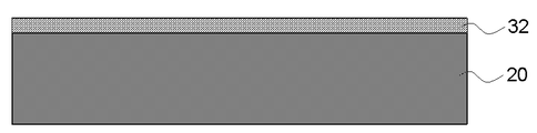
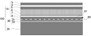
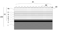
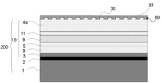
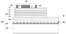
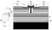
- the junction type semiconductor element 100 shown in FIG. 1 includes an epitaxial layer 10 and a support substrate 20.
- the epitaxial layer 10 and the support substrate 20 are joined via the joining layer 30.
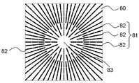
- the epitaxial layer 10 has a radial pattern 81 shown in FIG. 2 on the joint surface 80 with the support substrate 20.
- the radial pattern 81 is composed of a plurality of recesses 82 shown in FIGS. 1 and 2.
- the plurality of recesses 82 have a rectangular cross section. Further, as shown in FIG. 2, the plurality of recesses 82 extend radially around an arbitrary point 83 of the joint surface 80, thereby forming a radial pattern 81.
- the plurality of recesses 82 are discretely extended in a direction away from the center 83.
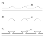
- FIG. 1 illustrates the case where the cross-sectional shape of the recess 82 is rectangular, but as illustrated in FIGS. 3A to 3C, the cross-sectional shape of the recess 82 may be triangular or trapezoidal. .. Further, the radial pattern 81 may be formed of convex portions instead of concave portions.
- the electrodes are generally installed in the center of the planned device area. Therefore, the center of the planned device area may be installed at a position corresponding to the center 83 of the radial pattern 81. Suitable. However, when it is preferable that the center 83 of the radial pattern 81 is located in the center of the planned device area, it is the case where there is one electrode, and when a plurality of electrodes are provided, this is not the case.
- the direction of expansion and contraction of the material due to thermal expansion and the center point vary depending on the electrode arrangement and the design, but the effect of the present invention can be obtained as long as the radial pattern 81 having an arbitrary point on the joint surface as the center 83 is provided. Therefore, the center 83 of the radial pattern 81 does not necessarily have to be set at the center or the center of gravity of the joint surface, and is not limited to being set at the center or the center of gravity of the joint surface.
- the center 83 of the radial pattern 81 is not particularly limited as long as it is an arbitrary point of the joint surface 81.
- the plurality of recesses 82 may be continuously extended in a direction away from the center 83.
- the radial pattern 81 can take various aspects with respect to the shape of the concave portion 82 or the convex portion and the position of the center 83, for example, as shown in FIGS. 2 and 4 (A) to 4 (E).
- the method for manufacturing a bonded semiconductor device of the present invention is a method for manufacturing a bonded semiconductor device in which an epitaxial layer and a support substrate made of a material different from the epitaxial layer are bonded.
- a radial pattern consisting of concave portions or convex portions extending radially around an arbitrary point is provided on either the joint surface of the epitaxial layer or the joint surface of the support substrate.
- the epitaxial layer is bonded to the support substrate by facing the bonding surface of the epitaxial layer and the bonding surface of the support substrate.
- the direction of expansion when heat is applied or the contraction when the temperature drops. It is possible to manufacture a bonded semiconductor device capable of controlling the expansion / contraction direction by facilitating the direction along the concave portion or the convex portion. As a result, the bonded semiconductor device manufactured by the method for manufacturing the bonded semiconductor device of the present invention can suppress the occurrence of peeling and fracture due to the rise and fall of the temperature.
- the bonded semiconductor device of the present invention described above can be manufactured.
- the radial pattern in which the depth of the concave portion or the height H of the convex portion is 0.02 ⁇ m or more and 5 ⁇ m or less.
- the H / L when the depth of the concave portion or the height of the convex portion is H and the width is L is 1 or more and 50 or less.
- Recesses or protrusions that extend continuously or discretely in the direction away from the center can be provided. In this way, it is possible to form a radial pattern consisting of various forms of recesses or protrusions.
- the radial pattern on the epitaxial layer side it is preferable to provide the radial pattern on the epitaxial layer side.
- the radial pattern on the epitaxial layer side it is possible to manufacture a bonded semiconductor device capable of further controlling the expansion and contraction directions of the epitaxial layer and further suppressing the occurrence of peeling and fracture due to the rise and fall of the temperature.
- a radial pattern for example, a radial pattern is formed on the joint surface of the epitaxial layer by a photolithography method, and based on the formed pattern, etching is performed by wet etching or dry etching so as to form a concave or convex pattern. Thereby, it can be formed.
- a resist pattern is formed on the joint surface by a photolithography method, and the resist pattern is used as a mask material for etching with a mixed solution of sulfuric acid or organic acid and a mixed solution of hydrochloric acid nitrate. , It is possible to form a radial pattern.
- a radial pattern can be formed by using the resist pattern as a mask material and treating it with, for example, chlorine-based plasma.
- the concave portion of the radial pattern is formed to a depth of about 1.0 ⁇ m, but the same effect can be obtained even if a step larger than this is provided.
- the acid-based etchant mixed with hydrogen peroxide attacks the resist, it can be formed by using another mask material such as SiO 2 when a step of 1.0 ⁇ m or more is provided.
- the starting substrate and the supporting substrate of the epitaxial layer AlN, Al 2 O 3, Cu, GaAs, GaN, GaP, InP, Si, those containing any of the materials selected from the group consisting of SiC and SiO 2 used,
- a material containing the above-mentioned material having a crystal structure is used.
- the support substrate one containing the above-mentioned material having a crystalline structure or an amorphous structure can be used. The present invention can be suitably adopted for such materials.
- the epitaxial layer can be bonded to the support substrate via a metal film or a thermosetting resin.
- a metal film or a thermosetting resin can be used as a bonding material for the bonding layer between the epitaxial layer and the support substrate.
- the metal film and the thermosetting resin for example, those described above can be used.
- junction-type semiconductor device of the present invention and the method for manufacturing the junction-type semiconductor element will be described in detail.
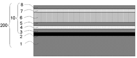
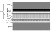
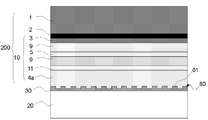
- an etch stop layer 2 is arranged between the starting substrate 1 and the epitaxial layer 10 shown in FIG. 5, and an epitaxial wafer (PV epitaxial wafer) 200 in which the epitaxial layer 10 has a PV (photovoltaic) structure is prepared.
- PV epitaxial wafer PV epitaxial wafer
- the PV epitaxial wafer 200 has a p-In x Ga 1-x P (0.4 ⁇ x ⁇ 0.6) etch stop layer 2 and a film thickness of 0.2 ⁇ m on the p-type GaAs starting substrate 1.
- the p-GaAs contact layer 3 has a thickness of 0.1 ⁇ m
- the p-In x Ga 1-x P (0.4 ⁇ x ⁇ 0.6) window layer 4 has a film thickness of 0.1 ⁇ m
- the film thickness is 0.
- a radial pattern is formed on the GaAs uneven cambium layer 8 which is the surface of the epitaxial wafer 200 along the planned device area size by a photolithography method, and based on the formed pattern, a recess or a recess is formed by wet or dry etching. Etching is performed so as to form a radial pattern consisting of convex portions.
- FIG. 6 shows an example in which a radial pattern 81 composed of a plurality of recesses 82 having a rectangular cross-sectional shape is formed on a joint surface 80 which is the surface of the uneven cambium 8.
- the radial pattern 81 is preferably provided with the depth of the recess 82 within the range of 0.02 to 5.0 ⁇ m.
- Such a radial pattern 81 can be formed, for example, by using a resist pattern as a mask material and etching with a mixed solution of sulfuric acid hydrogen peroxide or organic acid hydrogen peroxide.
- the radial pattern 81 is formed until the step becomes about 1.0 ⁇ m, but the same effect can be obtained even if a step larger than this is provided.
- the acid-based etchant mixed with hydrogen peroxide attacks the resist, it can be formed by using another mask material such as SiO 2 when a step of 1.0 ⁇ m or more is provided.
- the radial pattern 81 composed of a plurality of concave portions 82 is illustrated, but the radial pattern 81 may be composed of a convex portion or a concave portion.
- the H / L is preferably 1 or more and 50 or less.
- the radial pattern 81 shown in FIG. 4A is formed. More specifically, the formed radial pattern 81 is a pattern in which the center 83 of the radial pattern 81 is located at a position offset from the planned device area.
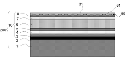
- a bonded metal film 31 is formed on the bonded surface 80, which is the surface of the uneven cambium 8 on which the radial pattern 81 is formed.
- the bonded metal film 31 can be formed of, for example, a metal layer made of Ti / Au.
- the Ti layer thickness can be, for example, 0.1 ⁇ m
- the Au layer can be, for example, 1.0 ⁇ m.
- the bonded metal film 31 for example, one containing a soft metal containing at least one kind of Ag, Al, Cu, Ga, In and the like including Au can be used. Any material can be selected as the soft metal.
- thermosetting resin such as benzocyclobutene (BCB) or polyimide (PI) may be used for bonding.
- a silicon wafer is prepared as the support substrate (bonded substrate) 20, and a bonded metal film 32 made of Ti / Au is formed on the surface of the support substrate 20 as shown in FIG.
- the Ti layer thickness can be, for example, 0.1 ⁇ m
- the Au layer can be, for example, 1.0 ⁇ m.
- bonded metal film 32 similarly to the bonded metal film 31, for example, a film containing a soft metal containing at least one kind of Ag, Al, Cu, Ga, In and the like including Au can be used. Any material can be selected as the soft metal.
- the bonded metal film 31 or 32 may have a structure having two or more metal layers including Ge, Si, etc. that facilitate ohmic contact. Further, in order to facilitate electrical contact, the same effect can be obtained with a structure in which a Ni-containing layer is provided between the semiconductor and the Ti layer.
- the epitaxial wafer 200 having the bonded metal film 31 and the support substrate 20 having the bonded metal film 32 are opposed to each other, and the bonded metal films 31 and 32 are overlapped and thermocompression bonded.
- the bonding temperature is preferably in the range of about 300 to 450 ° C. Further, it is preferable to join the joining pressure portion at 50 to 500 N / cm 2 or more.
- the above conditions are suitable for obtaining sufficient bonding strength, and may be a low temperature or a high temperature outside this range, a small bonding pressure, or a high bonding pressure.
- the starting substrate 1 (GaAs) was removed with an ammonia-superhydrated etchant, and after the starting substrate 1 was removed, the p-InGaP etching stop layer 2 was removed with a hydrochloric acid-based etchant, and as shown in FIG. The layer 3 is exposed.
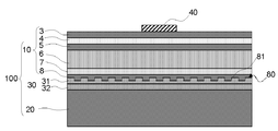
- the bonded semiconductor device 100 of the first embodiment of the present invention in which the epitaxial layer 10 and the support substrate 20 are bonded via the bonding layer 30 composed of the metal bonding layers 31 and 32, as shown in FIG. can get.
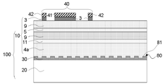
- an electrode 40 for energization is formed on the p-GaAs contact layer 3.
- the electrode 40 is configured to have a semicircular electrode 41 for a bonding pad and a branch electrode 42 for current extraction extending from the electrode 41 for the bonding pad.
- the electrodes 40 can be arranged in the order of the Zn-doped Au layer, the Ti layer, and the Au layer in order from the layer in contact with the p-GaAs contact layer 3.
- the Zn-doped Au layer thickness can be, for example, 0.1 ⁇ m
- the Ti layer can be, for example, 0.1 ⁇ m
- the Au layer can be, for example, 2.0 ⁇ m.
- an etch stop layer 2 is arranged between the starting substrate 1 and the epitaxial layer 10 shown in FIG. 13, and an epitaxial wafer (LED epitaxial wafer) 200 in which the epitaxial layer 10 has an LED structure is prepared.
- p-In x Ga 1-x P (0.4 ⁇ x ⁇ 0.6) etch stop layer 2 and p-GaAs are placed on the p-type GaAs starting substrate 1.
- a radial pattern is formed on the n-GaP window layer / concavo-convex forming layer 4a, which is the surface of the epitaxial wafer 200, by a photolithography method along the planned device area size, and wet or wet or based on the formed radial pattern.
- dry etching etching is performed so as to form a radial pattern consisting of concave portions or convex portions.
- FIG. 14 shows an example in which a radial pattern 81 composed of a plurality of recesses 82 having a rectangular cross-sectional shape is formed on a joint surface 80 which is a surface of a window layer and uneven cambium forming layer 4a.
- the radial pattern 81 is preferably provided with the depth of the recess 82 within the range of 0.02 to 5.0 ⁇ m.
- Such a radial pattern 81 can be formed, for example, by using a resist pattern as a mask material and treating it with a nitrate / hydrochloric acid mixed solution in the case of wet etching and a chlorine-based plasma in the case of dry etching.
- the radial pattern 81 is formed until the step becomes about 1.0 ⁇ m, but the same effect can be obtained even if a step larger than this is provided.
- the radial pattern 81 composed of a plurality of concave portions 82 is illustrated, but the radial pattern 81 may be composed of a convex portion or a concave portion.
- the H / L is preferably 1 or more and 50 or less.
- the radial pattern 81 shown in FIG. 4 (E) is formed.
- the formed radial pattern 81 is a pattern in which the central portion 83 of the radial pattern 81 is located at a position slightly offset from the planned device area.
- a bonding layer 30 made of BCB is formed by spin coating on the bonding surface 80, which is the surface of the window layer and uneven cambium forming layer 4a on which the radial pattern 81 is formed.
- the thickness of the bonding layer 30 made of BCB can be, for example, 2.0 ⁇ m.
- the thickness is merely an example, and any film thickness can be selected as long as it is equal to or larger than the step of the radial pattern 81.
- BCB is exemplified as the bonding material of the bonding layer 30, but the same effect can be obtained by using other translucent thermosetting materials such as PI, sol-gel liquid, and low-dielectric glass.
- a metal joining layer may be used as the joining material.
- the epitaxial wafer 200 having the BCB bonding layer 30 and the support substrate 20 are opposed to each other so as to sandwich the BCB bonding layer 30, and are superposed and thermocompression bonded.
- the BCB joining material may or may not be applied on the support substrate 20. Further, the BCB bonding material may not be applied to the epitaxial wafer 200 side, but may be applied only to the support substrate 20.
- thermocompression bonding is preferably performed in the range of 150 to 400 ° C. Further, it is preferable to join the joining pressure portion at 50 to 500 N / cm 2 or more.
- the above conditions are suitable for obtaining sufficient bonding strength, and may be a low temperature or a high temperature outside this range, a small bonding pressure, or a high bonding pressure.
- the starting substrate (GaAs) 1 is removed with an ammonia-superhydrated etchant, and after the starting substrate 1 is removed, the p-InGaP etching stop layer 2 is removed with a hydrochloric acid-based etchant to expose the p-GaAs contact layer 3.
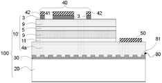
- the bonded semiconductor device 100 according to the second embodiment of the present invention in which the epitaxial layer 10 and the support substrate 20 are bonded via the bonding layer 30, as shown in FIG. 17, can be obtained.
- an upper electrode 40 for energization is formed on the p-GaAs contact layer 3, and the p-GaAs contact layer 3 in a region other than the electrode 40 is removed with sulfuric acid hydrogen peroxide or the like.
- the upper electrode 40 has a configuration in which a circular electrode 41 for a bonding pad is arranged and a branch electrode 42 for current extraction extending from the electrode 41 for the bonding pad is provided.
- a part of the epitaxial layer 10 outside the electrode 40 forming region is cut out to expose a part of the n-GaP window layer and uneven forming layer 4a as shown in FIG.
- FIG. 21 is a schematic plan view of the bonded semiconductor device according to the second embodiment after the lower electrode 50 is formed.
- the upper electrode 40 can be arranged in the order of the Zn-doped Au layer, the Ti layer, and the Au layer in order from the layer in contact with the p-GaAs contact layer 3.
- the Zn-doped Au layer thickness can be, for example, 0.1 ⁇ m
- the Ti layer can be, for example, 0.1 ⁇ m
- the Au layer can be, for example, 2.0 ⁇ m.
- the lower electrode 50 can be arranged in the order of the Ge-doped Au layer, the Ni layer, the Ti layer, and the Au layer in order from the layer in contact with the n-GaP window layer and the uneven cambium forming layer 4a.
- the Ge-doped Au layer thickness can be, for example, 0.1 ⁇ m
- the Ni layer can be, for example, 0.1 ⁇ m
- the Ti layer can be, for example, 0.1 ⁇ m
- the Au layer can be, for example, 2.0 ⁇ m.
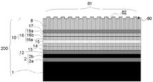
- an etch stop layer 2 is arranged between the starting substrate 1 and the epitaxial layer 10 shown in FIG. 22, and an epitaxial wafer (HEMT epitaxial wafer) 200 in which the epitaxial layer 10 has a HEMT structure is prepared.
- HEMT epitaxial wafer epitaxial wafer
- n + -In x Ga 1-x As (0.4 ⁇ x ⁇ 0.6) etch stop layers 2a and n are placed on the n-type InP starting substrate 1.
- Etch stop layer 2 composed of + -InP etch stop layer 2b, n + -InGaAs contact layer 12, n + -InAlAs layer 13, i-InAlAs layer 14, i-InP etch stop layer 15, Si delta dope ( ⁇ dope) layer It can be prepared by forming the i-InAlAs-containing layer 16, the i-InGaAs layer 17, and the i-InAlAs unevenness-forming layer 8 including the 16b and the two i-InAlAs layers 16a sandwiching the 16b in this order. ..
- a radial pattern is formed on the i-InAlAs uneven cambium 8 which is the surface of the epitaxial wafer 200 along the planned device area size by a photolithography method, and based on the formed pattern, wet or dry etching is performed. Etch to form a radial pattern consisting of recesses or bumps.
- FIG. 23 shows an example in which a radial pattern 81 composed of a plurality of recesses 82 having a rectangular cross-sectional shape is formed on the joint surface 80 which is the surface of the uneven cambium 8.
- the radial pattern 81 shown in FIG. 2 is formed.
- the formed radial pattern 81 is a pattern in which the central portion 83 of the radial pattern 81 is located at the central portion of the planned device area.
- the radial pattern 81 is preferably provided with the depth of the recess 82 within the range of 0.02 to 5.0 ⁇ m.
- Such a radial pattern 81 can be formed, for example, by using a resist pattern as a mask material and treating it with a nitrate / hydrochloric acid mixed solution in the case of wet etching and a chlorine-based plasma in the case of dry etching.
- the radial pattern 81 is formed until the step becomes about 1.0 ⁇ m, but the same effect can be obtained even if a step larger than this is provided.
- the radial pattern 81 composed of a plurality of concave portions 82 is illustrated, but the radial pattern 81 may be composed of a convex portion or a concave portion.
- the H / L is preferably 1 or more and 50 or less.
- a joint layer 30 made of BCB is formed by spin coating on the joint surface 80 which is the surface of the uneven cambium 8 on which the radial pattern 81 is formed.
- the thickness of the bonding layer 30 made of BCB can be, for example, 2.0 ⁇ m. Further, in the present embodiment, BCB is exemplified as the bonding material of the bonding layer 30, but the same effect can be obtained by using other translucent thermosetting materials such as PI, sol-gel liquid, and low-dielectric glass.
- a metal joining layer may be used as the joining material.
- the epitaxial wafer 200 having the BCB bonding layer 30 and the silicon wafer (supporting substrate) 20 are opposed to each other so as to sandwich the BCB bonding layer 30, and are superposed and thermocompression bonded.
- the BCB joining material may or may not be applied on the support substrate 20. Further, the BCB bonding material may not be applied to the epitaxial wafer 200 side, but may be applied only to the support substrate 20.
- thermocompression bonding is preferably performed in the range of 150 to 400 ° C. Further, it is preferable to join the joining pressure portion at 50 to 500 N / cm 2 or more.
- the above conditions are suitable for obtaining sufficient bonding strength, and may be a low temperature or a high temperature outside this range, a small bonding pressure, or a high bonding pressure.
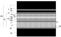
- the starting substrate (InP) 1 is removed with hydrochloric acid water, and after the starting substrate 1 is removed, the n + -InGaAs etching stop layer 2a is removed with phosphoric acid superwater, and then the n + -InP etching stop layer 2b. Is removed with hydrochloric acid water to expose the n + -InGaAs layer 12.
- the bonded semiconductor device 100 according to the third embodiment of the present invention in which the epitaxial layer 10 and the support substrate 20 are bonded via the bonding layer 30, as shown in FIG. 26, is obtained.
- a resist pattern in which the portion corresponding to the gate region is opened is formed on the n + -InGaAs layer 12 side of the epitaxial layer 10 by a photolithography method.
- this resist pattern as a mask, the portion of the n + -InGaAs layer 12 to the i-InAlAs layer 14 corresponding to the opening of the resist pattern is removed with phosphoric acid hydrogen peroxide. Since phosphoric acid hydrogen peroxide has etching selectivity for InP, a part of the InP layer 15 is removed with hydrochloric acid water to expose the i-InAlAs layer 16a, which is the lower layer of the InP layer 15, and then the resist is applied. Peel off.
- the SiN x (0 ⁇ x ⁇ 2) layer 18 is deposited at 100 nm on the gate region on the n + ⁇ InGaAs layer 12 and the portion corresponding to the periphery thereof.
- a resist pattern in which the drain region, the source region, and the gate region are opened is formed by a photolithography method, patterned with a fluoroacid-containing liquid, and then the resist is peeled off. More specifically, the desired pattern 300 shown in FIG. 27 is formed by photolithography, the electrode material is vapor-deposited, and then lift-off is performed. As shown in FIG. 28, the source electrode 44, the drain electrode 45, and the gate electrode are formed. 43 is formed in a lump.
- the structure of the electrode may be, for example, a Pt layer of, for example, 0.1 ⁇ m, a Ti layer of, for example, 0.1 ⁇ m, and an Au layer of, for example, 1.0 ⁇ m.
- a bonded semiconductor device 100 including a gate region 101, a source region 102, and a drain region 103 and having an epitaxial layer having a HEMT structure can be obtained.
- Example 1 a bonded semiconductor device having a structure similar to that shown in FIG. 11 was manufactured by the following procedure.
- an etch stop layer 2 was arranged between the p-type GaAs starting substrate 1 and the epitaxial layer 10 having the same structure as shown in FIG. 5, and a PV epitaxial wafer 200 having a PV (photovoltaic) structure in the epitaxial layer 10 was prepared. ..
- the PV epitaxial wafer 200 has a p-InGaP etch stop layer 2 having a film thickness of 0.2 ⁇ m, a p-GaAs contact layer 3 having a film thickness of 0.1 ⁇ m, and a film thickness of 0 on the p-type GaAs departure substrate 1. .1 ⁇ m p-InGaP window layer 4, p-GaAs emitter layer 5 with a film thickness of 0.5 ⁇ m, n-GaAs base layer 6 with a film thickness of 3.5 ⁇ m, p with a film thickness of 0.1 um -Prepared by forming the BSF layer 7 of InGaP and the GaAs unevenness forming layer 8 in this order.
- a radial pattern similar to that shown in FIG. 4A was formed on the GaAs unevenness forming layer 8 on the surface of the epitaxial wafer 200 along the planned device area size by a photolithography method, and the formed pattern was formed.
- a radial pattern 81 composed of recesses 82 was formed by dry etching (FIG. 6). As shown in FIG. 4A, the formed radial pattern 81 is a pattern in which the center 83 of the radial pattern is located at a position offset from the planned device area.
- Example 1 the depth of the recess 82 was set to 0.01 ⁇ m.
- the width was the same as the depth.
- a bonded metal film 31 was formed on the bonded surface 80, which is the surface of the uneven cambium 8 on which the radial pattern 81 was formed.
- the bonded metal film 31 was formed of a metal layer made of Ti / Au.
- the Ti layer thickness was 0.1 ⁇ m, and the Au layer was 1.0 ⁇ m.
- a silicon wafer was prepared as the support substrate (bonded substrate) 20, and as shown in FIG. 8, a bonded metal layer 32 made of Ti / Au was formed on the surface of the support substrate 20.
- the Ti layer thickness was 0.1 ⁇ m, and the Au layer was 1.0 ⁇ m.
- the epitaxial wafer 200 having the bonded metal film 31 and the support substrate 20 having the bonded metal film 32 are opposed to each other with the bonded metal films 31 and 32, and the temperature is 350 ° C., 300 N /. They were joined by thermocompression bonding at a pressure of cm 2.
- the starting substrate 1 (GaAs) was removed with an ammonia-superhydrated etchant, and after the starting substrate 1 was removed, the p-InGaP etching stop layer 2 was removed with a hydrochloric acid-based etchant, and as shown in FIG. 10, p-GaAs.
- the contact layer 3 was exposed.
- a bonded semiconductor device 100 in which the epitaxial layer 10 and the support substrate 20 shown in FIG. 10 were bonded via the bonded layer 30 composed of the bonded metal films 31 and 32 was obtained.
- an electrode 40 for energization was formed on the P-GaAs contact layer 3.
- the electrode 40 has a structure in which a semi-circular electrode 41 for a bonding pad is arranged and a branch electrode 42 for current extraction extending from the electrode 41 for the bonding pad is provided.
- the electrodes 40 were arranged in the order of the Zn-doped Au layer, the Ti layer, and the Au layer in order from the layer in contact with the p-GaAs contact layer 3.
- the Zn-doped Au layer thickness was 0.1 ⁇ m
- the Ti layer was 0.1 ⁇ m
- the Au layer was 2.0 ⁇ m.
- Examples 2 to 11 In Examples 2 to 11, the depths of the recesses of the radial pattern 81 are 0.02 ⁇ m (Example 2), 0.05 ⁇ m (Example 3), 0.1 ⁇ m (Example 4), and 0.2 ⁇ m (Example 4). 5), 0.5 ⁇ m (Example 6), 1.0 ⁇ m (Example 7), 2.0 ⁇ m (Example 8), 5.0 ⁇ m (Example 9), 6.0 ⁇ m (Example 10), 10 ⁇ m (Example 10) A bonded semiconductor device 100 having a structure similar to that shown in FIG. 11 was obtained by the same procedure as in Example 1 except that the change was made in Example 11).
- the bonded semiconductor elements 100 obtained in Examples 1 to 11 were made into chips by dicing, wiring was performed on the electrodes, a sealing material was injected, and packaging was performed. In order to soften the encapsulant, heat was applied to a temperature above the softening point for injection. After the injection, the temperature of the encapsulant was lowered to room temperature for packaging.
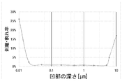
- FIG. 29 shows the relationship between the depth of the recess 81 and the chip cracking rate at that time.
- Example 12 The same chips as in Example 1 were produced except that the radial pattern 81 was formed into a radial pattern consisting of a plurality of convex portions having a height of 1 ⁇ m, and the same packaging as in Example 1 was performed. In Example 12, chip cracking did not occur.
- Comparative Example 1 The same chips as in Example 1 were produced except that the radial pattern 81 was not formed, and the same packaging as in Example 1 was performed. In Comparative Example 1, chip cracking occurred by 35%.
- Examples 1 to 12 in which the radial pattern was formed on the joint surface had a higher temperature than Comparative Example 1 in which the radial pattern was not formed on the joint surface. It was possible to suppress the occurrence of peeling and breakage due to ascent and descent. In particular, it can be seen that the results were good when the depth of the recess was 0.02 ⁇ m to 5 ⁇ m. Further, from the comparison between Example 7 and Example 12, it was possible to suppress the occurrence of peeling and breakage due to the rise and fall of the temperature, regardless of whether the radial pattern was composed of concave portions or convex portions. You can see that.
- Example 13 a bonded semiconductor device having a structure similar to that shown in FIG. 20 was manufactured by the following procedure.
- an etch stop layer 2 was arranged between the p-type GaAs departure substrate 1 and the epitaxial layer 10 as shown in FIG. 13, and an LED epitaxial wafer 200 in which the epitaxial layer 10 had an LED structure was prepared.
- the p-InGaP etch stop layer 2 As the LED epitaxial wafer 200, as shown in FIG. 13, the p-InGaP etch stop layer 2, the p-GaAs contact layer 3, the p-AlGaInP clad layer 9, and the i-AlGaInP active layer 5 are placed on the p-type GaAs substrate 1.
- N-AlGaInP clad layer 9, n-InGaP intermediate layer 11, n-GaP window layer and concavo-convex forming layer 4a were prepared in this order.
- a radial pattern is formed on the GaP window layer and uneven cambium 4a, which is the surface of the epitaxial wafer 200, by a photolithography method along the planned device area size, and chlorine-based plasma is used based on the formed radial pattern.
- a radial pattern 81 composed of recesses 82 having a depth of 1 ⁇ m and a width of 1 ⁇ m was formed by dry etching.
- the obtained radial pattern 81 was the same pattern as that shown in FIG. 4 (E).
- a bonding layer 30 made of BCB having a thickness of 2.0 ⁇ m is formed on the bonding surface 80, which is the surface of the window layer and uneven forming layer 4a on which the radial pattern 81 is formed, by spin coating. did.
- a sapphire substrate is prepared as the support substrate (bonded substrate) 20, and as shown in FIG. 16, the epitaxial wafer 200 having the BCB bonding layer 30 and the support substrate 20 are opposed to each other so as to sandwich the BCB bonding layer 30. , And joined by thermocompression bonding at a temperature of 350 ° C. and a pressure of 300 N / cm 2.
- the starting substrate (GaAs) 1 was removed with an ammonia-superhydrated etchant, and after the starting substrate 1 was removed, the p-InGaP etching stop layer 2 was removed with a hydrochloric acid-based etchant to expose the p-GaAs contact layer 3.
- the bonded semiconductor device 100 in which the epitaxial layer 10 and the support substrate 20 were bonded via the bonding layer 30 as shown in FIG. 17 was obtained.
- an upper electrode 40 for energization was formed on the p-GaAs contact layer 3, and the p-GaAs contact layer 3 in a region other than the electrode 40 was removed with sulfuric acid hydrogen peroxide or the like.
- the upper electrode 40 has a structure in which a circular electrode 41 for a bonding pad is arranged and a branch electrode 42 for current extraction extending from the electrode 41 for the bonding pad is provided.
- the lower electrode 50 was formed on a part of the exposed n-GaP window layer and uneven cambium 4a.
- the upper electrode 40 was arranged in the order of the Zn-doped Au layer, the Ti layer, and the Au layer in order from the layer in contact with the p-GaAs contact layer 3.
- the Zn-doped Au layer thickness was 0.1 ⁇ m
- the Ti layer was 0.1 ⁇ m
- the Au layer was 2.0 ⁇ m.
- the lower electrode 50 was arranged in the order of the Ge-doped Au layer, the Ni layer, the Ti layer, and the Au layer in order from the layer in contact with the n-GaP window layer and the uneven cambium layer 4a.
- the thickness of the Ge-doped Au layer was 0.1 ⁇ m
- the Ni layer was 0.1 ⁇ m
- the Ti layer was 0.1 ⁇ m
- the Au layer was 2.0 ⁇ m.
- the junction-type semiconductor device 100 obtained in Example 13 was made into a chip by dicing, wiring was performed on the electrodes, a sealing material was injected, and packaging was performed. In order to soften the encapsulant, heat was applied to a temperature above the softening point for injection. After the injection, the temperature of the encapsulant was lowered to room temperature for packaging. When the chip cracking was investigated, no chip cracking occurred.
- Example 14 A chip similar to that of Example 13 was produced except that the radial pattern 81 was formed into a radial pattern composed of a plurality of convex portions having a height of 1 ⁇ m, and packaging was performed in the same manner as in Example 13. In Example 14, chip cracking did not occur.
- Comparative Example 2 The same chips as in Example 13 were prepared except that the radial pattern 81 was not formed, and the same packaging as in Example 13 was performed. In Comparative Example 2, chip cracking occurred by 30%.
- Examples 13 and 14 in which the radial pattern was formed on the joint surface had more peeling and fracture due to the rise and fall of the temperature than Comparative Example 2 in which the radial pattern was not formed on the joint surface. The outbreak could be suppressed. Further, from the comparison between Example 13 and Example 14, it was possible to suppress the occurrence of peeling and breakage due to the rise and fall of the temperature, regardless of whether the radial pattern was composed of concave portions or convex portions. You can see that.
- Example 15 a bonded semiconductor device having a structure similar to that shown in FIG. 28 was manufactured by the following procedure.
- an etch stop layer 2 was arranged between the n-type InP starting substrate 1 and the epitaxial layer 10 as shown in FIG. 22, and a HEMT epitaxial wafer 200 in which the epitaxial layer 10 had a HEMT structure was prepared.
- the etch stop layer 2 and n + -InGaAs composed of the n + -InGaAs etch stop layer 2a and the n-InP etch stop layer 2b are placed on the n-type InP starting substrate 1.
- An i-InAlAs-containing layer including a contact layer 12, an n + -InAlAs layer 13, an i-InAlAs layer 14, an i-InP etch stop layer 15, a Si delta-doped layer 16b, and two i-InAlAs layers 16a sandwiching the contact layer 12. 16.
- the i-InGaAs layer 17 and the i-InAlAs unevenness-forming layer 8 were formed in this order.
- a radial pattern similar to that shown in FIG. 2 was formed on the i-InAlAs uneven cambium 8 on the surface of the epitaxial wafer 200 along the planned device area size by a photolithography method, and the formed pattern was formed. Based on this, as shown in FIG. 23, a radial pattern 81 composed of a plurality of recesses 82 having a depth of 1 ⁇ m and a width of 1 ⁇ m was formed by dry etching using a chlorine-based plasma. The obtained radial pattern 81 was the same pattern as that shown in FIG.
- a bonding layer 30 made of BCB having a thickness of 2.0 ⁇ m was formed on the bonding surface 80, which is the surface of the uneven forming layer 8 on which the radial pattern 81 was formed, by spin coating.
- a silicon wafer is prepared as a support substrate (bonded substrate), and as shown in FIG. 25, the epitaxial wafer 200 having the BCB bonding layer 30 and the support substrate 20 are opposed to each other so as to sandwich the BCB bonding layer 30. They were overlapped and bonded by thermocompression bonding at a temperature of 350 ° C. and a pressure of 300 N / cm 2.
- the starting substrate (InP) 1 is removed with hydrochloric acid water, and after the starting substrate 1 is removed, the n + -InGaAs etching stop layer 2a is removed with phosphoric acid superwater, and then the n + -InP etching stop layer 2b.
- the bonded semiconductor device 100 in which the epitaxial layer 10 and the support substrate 20 were bonded via the bonding layer 30 as shown in FIG. 26 was obtained.
- a resist pattern in which the portion corresponding to the gate region was opened was formed on the n + -InGaAs layer 12 side of the epitaxial layer 10 by a photolithography method.
- this resist pattern as a mask, the portion of the n + -InGaAs layer 12 to the i-InAlAs layer 14 corresponding to the opening of the resist pattern was removed by phosphoric acid hydrogen peroxide.
- a part of the InP layer 15 was removed with hydrochloric acid water to expose the i-InAlAs layer 16a, which is the lower layer of the InP15, and then the resist was peeled off.
- the SiN x (0 ⁇ x ⁇ 2) layer 18 was deposited at 100 nm on the gate region on the n + ⁇ InGaAs layer 12 and the portion corresponding to the periphery thereof.
- a resist pattern in which the drain region, the source region, and the gate region were opened was formed by a photolithography method, patterned with a fluoroacid-containing liquid, and then the resist was peeled off. More specifically, the desired pattern 300 shown in FIG. 27 is formed by photolithography, the electrode material is vapor-deposited, and then lift-off is performed. As shown in FIG. 28, the source electrode 44 and the drain electrode 45, The gate electrodes 43 were collectively formed.
- the structure of the electrode was such that a Pt layer of 0.1 ⁇ m, a Ti layer of 0.1 ⁇ m, and an Au layer of 1.0 ⁇ m were laminated.
- the junction-type semiconductor device 100 obtained in Example 15 was made into a chip by dicing, wiring was performed on the electrodes, a sealing material was injected, and packaging was performed. In order to soften the encapsulant, heat was applied to a temperature above the softening point for injection. After the injection, the temperature of the encapsulant was lowered to room temperature for packaging. When the chip cracking was investigated, no chip cracking occurred.
- Example 16 The same chips as in Example 15 were produced except that the radial pattern 81 was formed into a radial pattern consisting of a plurality of convex portions having a height of 1 ⁇ m, and the same packaging as in Example 15 was performed. In Example 16, chip cracking did not occur.
- Comparative Example 3 The same chips as in Example 15 were prepared except that the radial pattern 81 was not formed, and the same packaging as in Example 15 was performed. In Comparative Example 3, chip cracking occurred by 30%.
- Examples 15 and 16 in which the radial pattern was formed on the joint surface had more peeling and fracture due to the rise and fall of the temperature than in Comparative Example 3 in which the radial pattern was not formed on the joint surface. The outbreak could be suppressed. Further, from the comparison between Example 15 and Example 16, it was possible to suppress the occurrence of peeling and breakage due to the rise and fall of the temperature, regardless of whether the radial pattern was composed of concave portions or convex portions. You can see that.
- the present invention is not limited to the above embodiment.
- the above-described embodiment is an example, and any of the above-described embodiments having substantially the same configuration as the technical idea described in the claims of the present invention and having the same effect and effect is the present invention. Is included in the technical scope of.
Landscapes
- Led Devices (AREA)
- Recrystallisation Techniques (AREA)
- Photovoltaic Devices (AREA)
- Junction Field-Effect Transistors (AREA)
Abstract
本発明は、エピタキシャル層と該エピタキシャル層とは異なる材料の支持基板とが接合された接合型半導体素子であって、前記エピタキシャル層及び前記支持基板の何れか一方が、接合面に任意の点を中心として放射状に広がっている凹部または凸部からなる放射状パターンを有するものであることを特徴とする接合型半導体素子である。これにより、温度の上昇・下降による剥離や破壊の発生を抑制できる接合型半導体素子を提供できる。
Description
本発明は、接合型半導体素子及び接合型半導体素子の製造方法に関する。
化合物半導体の持つ特性と他の機能性基板とを接合することにより得られる新規機能性基板としての接合型半導体素子が各種提案されている。
IoT用センサーでは、駆動基板を有するシリコン基板上に、受電源として太陽電池(PV)を、信号受信部としてフォトダイオード(PD)を、信号発信部としてレーザーダイオード(LD)や発光ダイオード(LED)を実装して、機能性チップが実現できる。
発光ダイオードにおいては、シリコン基板に金属接合で発光層を接合したLEDが、あるいは透明なサファイア基板に透明接着剤で発光層を接合したLEDが提案されている。
いずれの構造においても、線膨脹係数や屈折率など、異なる物性を有する材料同士を接合し、実現している特徴がある。
異種材料同士を接合する技術では接合材そのものが着目されてきた。接合後のデバイスではパッケージを行う必要があり、パッケージプロセス、あるいはパッケージ後の動作過程において、少なからず熱履歴を受けるため、異種材料に伴う物性の違いから不良を引き起こすことがあった。
発生しやすい不良が、接合面からの薄膜部たる化合物半導体機能層(エピタキシャル層)部の剥離、及び、破壊である。
デバイス層(機能層)を含んだエピタキシャル層と、このエピタキシャル層とは異なる材料の支持基板とを接合させた構造を有する接合型半導体素子では、接合時の温度と動作温度あるいは室温との間に差異が存在するため、エピタキシャル層と支持基板との間には残留応力が存在する。接合型半導体素子は、動作による温度変化もしくは環境温度の変化により、膨張及び収縮を繰り返すため、接合界面からのエピタキシャル層の剥離が生じやすくなる。その結果、接合型半導体素子の動作不良が発生し、信頼性が低下する問題があった。その具体例を以下に示す。
封止材を注入し、パッケージングを行う際、封止材を軟化するため、軟化点以上の温度まで熱を加えて注入を行う。注入後は軟化点以下(一般には室温)まで封止材の温度を下げ、パッケージングを行う。
封止材の注入過程で、機能部であるエピタキシャル層(化合物半導体)部、接合部、支持部である支持基板部のそれぞれに同様の温度がかかり、室温低下時に、それぞれの物性値に従って収縮する。熱膨脹係数は一般に同一でないため、それぞれの部位において熱収縮に伴う応力を抱えることになる。
応力が過大に大きい場合、パッケージ直後に不良として検知が可能である。しかし、パッケージ直後に破壊が起こらなかった場合、通電し、動作することによるパッケージ内の温度の上昇・下降により、除々に剥離または破壊が進む。時間が経過した後、剥離や破壊が発生し、デバイスが動作不良となってしまう。
単体部品の場合の不良は1個だけにとどまるが、複数の機能性部を1チップに実装した場合、影響はチップ全体に及び、1個の機能部の剥離・故障によりシステム全体の故障に結びついてしまう。
これらの問題を解決するためには、支持基板とエピタキシャル層とを構成する材料の熱膨張係数を略同一にすることが有効だが、熱膨張係数を揃えつつ、その他の物性値を変えた材料を選択することは不可能である。
ゆえに、デバイスを動作させるための機能を有する材料を選択し、保持等の目的で異種材料基板に接合する構造を有する接合型半導体素子において、温度変化による膨張及び収縮の影響を極小化する構成、または構造が必要であった。
本発明は、上記の課題に鑑みてなされたもので、温度の上昇・下降による剥離や破壊の発生を抑制できる接合型半導体素子、及び温度の上昇・下降による剥離や破壊の発生の抑制が可能な接合型半導体素子を製造できる製造方法を提供することを目的とする。
上記目的を達成するために、本発明では、エピタキシャル層と該エピタキシャル層とは異なる材料の支持基板とが接合された接合型半導体素子であって、
前記エピタキシャル層及び前記支持基板の何れか一方が、接合面に任意の点を中心として放射状に広がっている凹部または凸部からなる放射状パターンを有するものであることを特徴とする接合型半導体素子を提供する。
前記エピタキシャル層及び前記支持基板の何れか一方が、接合面に任意の点を中心として放射状に広がっている凹部または凸部からなる放射状パターンを有するものであることを特徴とする接合型半導体素子を提供する。
このように凹部または凸部からなる放射状のパターンを接合面に設けておくことにより、熱が加わった時の膨張の方向、または温度が下がった時の収縮の方向が、凹部または凸部に沿って進みやすくなり、膨張収縮方向を制御することができる。その結果、本発明の接合型半導体素子は、温度の上昇・下降による剥離や破壊の発生を抑制できる。
前記放射状パターンの前記凹部の深さまたは前記凸部の高さHが0.02μm以上5μm以下のものであることが好ましい。
放射状パターンの凹部の深さまたは凸部の高さHを0.02μm以上5μm以下とすることにより、温度の上昇・下降による剥離や破壊の発生を更に抑制できる。
前記放射状パターンの前記凹部または前記凸部は、前記中心から遠ざかる方向において、連続的または離散的に延びているものとすることができる。
このように、凹部または凸部の形態は、特に限定されず、様々な態様をとることができる。
前記放射状パターンは、前記エピタキシャル層側に設けられていることが好ましい。
放射状パターンがエピタキシャル層側に設けられている接合型半導体素子であれば、温度の上昇・下降による剥離や破壊の発生を更に抑制できる。
前記支持基板が、AlN、Al2O3、Cu、GaAs、GaN、GaP、InP、Si、SiC及びSiO2からなる群より選択されるいずれかの材料を含み、
前記支持基板は、結晶構造または非晶質の構造を有する前記材料を含むものとすることができる。
前記支持基板は、結晶構造または非晶質の構造を有する前記材料を含むものとすることができる。
このような材料に対し、本発明を好適に採用することができる。
前記エピタキシャル層が金属膜または熱硬化型樹脂を介して前記支持基板に接合されたものとすることできる。
エピタキシャル層と支持基板との間の接合層の接合材として、例えば金属膜または熱硬化型樹脂を用いることができる。
また、本発明では、エピタキシャル層と、前記エピタキシャル層とは異なる材料の支持基板とが接合された接合型半導体素子の製造方法であって、
前記エピタキシャル層の接合面及び前記支持基板の接合面の何れか一方に、任意の点を中心として放射状に広がる凹部または凸部からなる放射状パターンを設け、
前記エピタキシャル層の前記接合面と前記支持基板の前記接合面とを向き合わせて、前記エピタキシャル層を前記支持基板に接合することを特徴とする接合型半導体素子の製造方法を提供する。
前記エピタキシャル層の接合面及び前記支持基板の接合面の何れか一方に、任意の点を中心として放射状に広がる凹部または凸部からなる放射状パターンを設け、
前記エピタキシャル層の前記接合面と前記支持基板の前記接合面とを向き合わせて、前記エピタキシャル層を前記支持基板に接合することを特徴とする接合型半導体素子の製造方法を提供する。
このように凹部または凸部からなる放射状のパターンを接合面に設けて、エピタキシャル層と支持基板とを接合することにより、熱が加わった時の膨張の方向、または温度が下がった時の収縮の方向が、凹部または凸部に沿って進みやすくなり、膨張収縮方向を制御することができる接合型半導体素子を製造できる。その結果、本発明の接合型半導体素子の製造方法によって製造した接合型半導体素子は、温度の上昇・下降による剥離や破壊の発生を抑制できる。
前記凹部の深さまたは前記凸部の高さHが0.02μm以上5μm以下である前記放射状パターンを設けることが好ましい。
凹部の深さまたは凸部の高さHが0.02μm以上5μm以下である放射状パターンを設けることにより、温度の上昇・下降による剥離や破壊の発生を更に抑制可能な接合型半導体素子を製造できる。
前記中心から遠ざかる方向において連続的または離散的に延びる前記凹部または前記凸部を設けることができる。
このように、様々な形態の凹部または凸部からなる放射状パターンを形成することができる。
前記放射状パターンを前記エピタキシャル層側に設けることが好ましい。
エピタキシャル層側に放射状パターンを設けることにより、温度の上昇・下降による剥離や破壊の発生を更に抑制可能な接合型半導体素子を製造できる。
前記エピタキシャル層の出発基板及び前記支持基板として、AlN、Al2O3、Cu、GaAs、GaN、GaP、InP、Si、SiC及びSiO2からなる群より選択されるいずれかの材料を含むものを用い、
前記エピタキシャル層の前記出発基板として、結晶構造を有する前記材料を含むものを用い、
前記支持基板として、結晶構造または非晶質の構造を有する前記材料を含むものを用いることができる。
前記エピタキシャル層の前記出発基板として、結晶構造を有する前記材料を含むものを用い、
前記支持基板として、結晶構造または非晶質の構造を有する前記材料を含むものを用いることができる。
このような材料に対し、本発明を好適に採用することができる。
前記エピタキシャル層を、金属膜または熱硬化型樹脂を介して前記支持基板に接合することができる。
エピタキシャル層と支持基板との間の接合層の接合材として、例えば金属膜または熱硬化型樹脂を用いることができる。
以上のように、本発明の接合型半導体素子であれば、膨張収縮方向を制御することができるので、温度の上昇・下降による剥離や破壊の発生を抑制できる。よって、本発明の接合型半導体素子は、優れた信頼性を示すことができる。
また、本発明の接合型半導体素子の製造方法であれば、膨張収縮方向を制御して、温度の上昇・下降による剥離や破壊の発生の抑制が可能な接合型半導体素子を製造できる。よって、本発明の接合型半導体素子の製造方法によれば、例えば光無線受電素子、太陽電池、発光素子、受光素子等の用途に適用できる、信頼性に優れた接合型半導体素子を製造できる。
上述のように、温度の上昇・下降による剥離や破壊の発生を抑制できる接合型半導体素子、及びこのような接合型半導体素子を製造できる製造方法の開発が求められていた。
本発明者らは、上記課題について鋭意検討を重ねた結果、エピタキシャル層とこのエピタキシャル層とは異なる材料の支持基板とを接合して接合型半導体素子にするに際し、凹部または凸部からなる放射状のパターンを接合面に設けて、エピタキシャル層と支持基板とを接合することにより、熱が加わった時の膨張の方向、または温度が下がった時の収縮の方向が、凹部または凸部に沿って進みやすくなり、膨張収縮方向を制御することができることを見出し、本発明を完成させた。
即ち、本発明は、エピタキシャル層と該エピタキシャル層とは異なる材料の支持基板とが接合された接合型半導体素子であって、
前記エピタキシャル層及び前記支持基板の何れか一方が、接合面に任意の点を中心として放射状に広がっている凹部または凸部からなる放射状パターンを有するものであることを特徴とする接合型半導体素子である。
前記エピタキシャル層及び前記支持基板の何れか一方が、接合面に任意の点を中心として放射状に広がっている凹部または凸部からなる放射状パターンを有するものであることを特徴とする接合型半導体素子である。
また、本発明は、エピタキシャル層と、前記エピタキシャル層とは異なる材料の支持基板とが接合された接合型半導体素子の製造方法であって、
前記エピタキシャル層の接合面及び前記支持基板の接合面の何れか一方に、任意の点を中心として放射状に広がる凹部または凸部からなる放射状パターンを設け、
前記エピタキシャル層の前記接合面と前記支持基板の前記接合面とを向き合わせて、前記エピタキシャル層を前記支持基板に接合することを特徴とする接合型半導体素子の製造方法である。
前記エピタキシャル層の接合面及び前記支持基板の接合面の何れか一方に、任意の点を中心として放射状に広がる凹部または凸部からなる放射状パターンを設け、
前記エピタキシャル層の前記接合面と前記支持基板の前記接合面とを向き合わせて、前記エピタキシャル層を前記支持基板に接合することを特徴とする接合型半導体素子の製造方法である。
なお、特許文献1には、透明基板と発光スタックとを例えばベンゾシクロブテン(BCB)などの透明接着層を介して接合してなる発光装置において、接合部が例えば粗面、凹凸またはピラミッド形状などの微細な突起を有するものが開示されている。しかしながら、特許文献1に記載された凹凸などの配置はランダムであり、膨張・収縮方向を制御できず、特許文献1は、放射状に広がった凹部または凸部からなる放射状パターンを記載も示唆もしていない。
以下、本発明について図面を参照しながら詳細に説明するが、本発明はこれらに限定されるものではない。
[接合型半導体素子]
本発明の接合型半導体素子は、エピタキシャル層と該エピタキシャル層とは異なる材料の支持基板とが接合された接合型半導体素子であって、
前記エピタキシャル層及び前記支持基板の何れか一方が、接合面に任意の点を中心として放射状に広がっている凹部または凸部からなる放射状パターンを有するものであることを特徴とする。
本発明の接合型半導体素子は、エピタキシャル層と該エピタキシャル層とは異なる材料の支持基板とが接合された接合型半導体素子であって、
前記エピタキシャル層及び前記支持基板の何れか一方が、接合面に任意の点を中心として放射状に広がっている凹部または凸部からなる放射状パターンを有するものであることを特徴とする。
このように凹部または凸部からなる放射状のパターンを接合面に設けておくことにより、熱が加わった時の膨張の方向、または温度が下がった時の収縮の方向が、凹部または凸部に沿って放射状に進みやすくなり、膨張収縮方向を制御することができる。その結果、本発明の接合型半導体素子は、温度の上昇・下降による剥離や破壊の発生を抑制できる。
特に、機能層部であるエピタキシャル層は薄膜であり得、延性を有しやすい半面、支持基板の延性方向とは必ずしも一致しない。特にエピタキシャル層の結晶軸が傾斜している場合、支持基板の延性方向とは大きく異なる場合が多い。
この場合、熱膨張の方向が一致しないため、破壊や剥離が起こりやすいが、接合面に凹部または凸部からなる放射状パターンを設けてやることにより、剥離や破壊を起こすことを抑制または、剥離や破壊が発生する加工時の臨界温度を上昇させることができる。
放射状パターンの凹部の深さまたは凸部の高さHが0.02μm以上5μm以下のものであることが好ましい。
放射状パターンの凹部の深さまたは凸部の高さHを0.02μm以上5μm以下とすることにより、温度の上昇・下降による剥離や破壊の発生を確実に抑制できる。
放射状パターンの凹部の深さまたは凸部の高さHを0.02μm以上5μm以下とすることにより、温度の上昇・下降による剥離や破壊の発生を確実に抑制できる。
放射状パターンは、凸部からなっていても、凹部からなっていてもどちらでも構わないが、パターンの横幅と深さ(段差)のサイズ及びアスペクト比は接合材が侵入できるものに設定しておく必要がある。凹部の深さまたは凸部の高さをH、幅をLとした時のH/Lが1以上50以下となるものが好ましい。
放射状パターンの凹部または凸部は、中心から遠ざかる方向において、連続的または離散的に延びているものとすることができる。
このように、凹部または凸部の形態は、特に限定されず、様々な態様をとることができる。
このように、凹部または凸部の形態は、特に限定されず、様々な態様をとることができる。
放射状パターンは、エピタキシャル層側に設けられていることが好ましい。
放射状パターンがエピタキシャル層側に設けられている接合型半導体素子であれば、エピタキシャル層の膨張及び収縮方向をより制御でき、温度の上昇・下降による剥離や破壊の発生を更に抑制できる。
放射状パターンがエピタキシャル層側に設けられている接合型半導体素子であれば、エピタキシャル層の膨張及び収縮方向をより制御でき、温度の上昇・下降による剥離や破壊の発生を更に抑制できる。
支持基板が、AlN、Al2O3、Cu、GaAs、GaN、GaP、InP、Si、SiC及びSiO2からなる群より選択されるいずれかの材料を含み、支持基板は、結晶構造または非晶質の構造を有する上記材料を含むものとすることができる。
このような材料に対し、本発明を好適に採用することができる。
このような材料に対し、本発明を好適に採用することができる。
エピタキシャル層が金属膜または熱硬化型樹脂を介して支持基板に接合されたものとすることできる。
エピタキシャル層と支持基板との間の接合材として、例えば金属膜または熱硬化型樹脂を用いることができる。もちろん、これらの他の接合材を用いても構わない。
エピタキシャル層と支持基板との間の接合材として、例えば金属膜または熱硬化型樹脂を用いることができる。もちろん、これらの他の接合材を用いても構わない。
接合材の金属膜としては、例えば、Au、Ag、Al、Cu、Ga、及びInからなる群より選択される少なくとも一種類の軟金属を含むものが挙げられる。金属膜は、Ti層などの金属層を更に含んでいても良い。
あるいは、金属膜は、オーミックコンタクトを容易ならしめるGeやSiなどを含む金属層を2層以上有する構造を含むものであってもよい。エピタキシャル層または支持基板に接する側に、電気コンタクトを容易にするために、Ni含有層を含んだものであっても、同様の効果が得られる。
熱硬化型樹脂としては、例えば、ベンゾシクロブテンやポリイミドを挙げることができる。
本発明の接合型半導体素子は、様々な用途に適用できる。例えば、本発明の接合型半導体素子は、例えば、光無線受電素子、太陽電池、発光素子、受光素子等の接合型半導体として、有用である。
次に、図1~図4を参照しながら、本発明の接合型半導体素子の幾つかの例を具体的に説明する。
図1に示す接合型半導体素子100は、エピタキシャル層10と、支持基板20とを含む。エピタキシャル層10と支持基板20とは、接合層30を介して、接合されている。
エピタキシャル層10は、支持基板20との接合面80に、図2に示す放射状パターン81を有する。放射状パターン81は、図1及び図2に示す、複数の凹部82からなる。
複数の凹部82は、図1に示すように、矩形の断面を有している。また、複数の凹部82は、図2に示すように、接合面80の任意の点83を中心として放射状に広がっており、それにより、放射状パターン81を構成している。
図2に示す例では、複数の凹部82は、中心83から遠ざかる方向において、離散的に延びている。
図1では、凹部82の断面形状が矩形である場合を例示しているが、図3(A)~(C)に例示するように、凹部82の断面形状は三角形や台形であっても良い。また、放射状パターン81は、凹部ではなく凸部からなるものでもよい。
また、デバイス予定エリアが正方形パターンの場合、電極をデバイス予定エリア中心部に設置することが一般的であるため、デバイス予定エリア中心部を放射状パターン81の中心83に対応する位置に設置することが好適である。ただし、放射状パターン81の中心83がデバイス予定エリア中心部にあることが好適である場合は電極が1個の場合であり、電極が複数設けられる場合は、この限りでは無い。熱膨張による材料伸縮方向や中心点は電極配置やデザインにより変わるが、接合面の任意の点を中心83とした放射状パターン81を設けたものであれば、本発明の効果が得られる。そのため、放射状パターン81の中心83は、必ずしも接合面の中心や重心に設定されることは必要なく、接合面の中心や重心に設定することに限定されない。
よって、放射状パターン81の中心83は、接合面81の任意の点であれば、特に限定されない。
また、例えば図4(A)に示すように、複数の凹部82は、中心83から遠ざかる方向において、連続的に延びたものでもよい。
すなわち、放射状パターン81は、凹部82または凸部の形状、並びに中心83の位置に関し、例えば図2及び図4(A)~(E)に示すように、様々な態様をとることができる。
[接合型半導体素子の製造方法]
本発明の接合型半導体素子の製造方法は、エピタキシャル層と、前記エピタキシャル層とは異なる材料の支持基板とが接合された接合型半導体素子の製造方法であって、
前記エピタキシャル層の接合面及び前記支持基板の接合面の何れか一方に、任意の点を中心として放射状に広がる凹部または凸部からなる放射状パターンを設け、
前記エピタキシャル層の前記接合面と前記支持基板の前記接合面とを向き合わせて、前記エピタキシャル層を前記支持基板に接合することを特徴とする。
本発明の接合型半導体素子の製造方法は、エピタキシャル層と、前記エピタキシャル層とは異なる材料の支持基板とが接合された接合型半導体素子の製造方法であって、
前記エピタキシャル層の接合面及び前記支持基板の接合面の何れか一方に、任意の点を中心として放射状に広がる凹部または凸部からなる放射状パターンを設け、
前記エピタキシャル層の前記接合面と前記支持基板の前記接合面とを向き合わせて、前記エピタキシャル層を前記支持基板に接合することを特徴とする。
このように凹部または凸部からなる放射状のパターンを接合面に設けて、エピタキシャル層と支持基板とを接合することにより、熱が加わった時の膨張の方向、または温度が下がった時の収縮の方向が、凹部または凸部に沿って進みやすくなり、膨張収縮方向を制御することが可能な接合型半導体素子を製造できる。その結果、本発明の接合型半導体素子の製造方法によって製造した接合型半導体素子は、温度の上昇・下降による剥離や破壊の発生を抑制できる。
本発明の接合型半導体素子の製造方法によると、先に説明した本発明の接合型半導体素子を製造することができる。
凹部の深さまたは凸部の高さHが0.02μm以上5μm以下である前記放射状パターンを設けることが好ましい。
凹部の深さまたは凸部の高さHが0.02μm以上5μm以下である放射状パターンを設けることにより、温度の上昇・下降による剥離や破壊の発生を更に抑制可能な接合型半導体素子を製造できる。
凹部の深さまたは凸部の高さHが0.02μm以上5μm以下である放射状パターンを設けることにより、温度の上昇・下降による剥離や破壊の発生を更に抑制可能な接合型半導体素子を製造できる。
凸部からなる放射状パターンを形成しても、凹部からなる放射状パターンを形成しても構わない。先に説明したように、凹部の深さまたは凸部の高さをH、幅をLとした時のH/Lが1以上50以下とするのが好ましい。
中心から遠ざかる方向において連続的または離散的に延びる凹部または凸部を設けることができる。
このように、様々な形態の凹部または凸部からなる放射状パターンを形成することができる。
このように、様々な形態の凹部または凸部からなる放射状パターンを形成することができる。
この場合、放射状パターンをエピタキシャル層側に設けることが好ましい。
エピタキシャル層側に放射状パターンを設けることにより、エピタキシャル層の膨張及び収縮方向をより制御でき、温度の上昇・下降による剥離や破壊の発生を更に抑制可能な接合型半導体素子を製造できる。
エピタキシャル層側に放射状パターンを設けることにより、エピタキシャル層の膨張及び収縮方向をより制御でき、温度の上昇・下降による剥離や破壊の発生を更に抑制可能な接合型半導体素子を製造できる。
放射状パターンは、例えば、エピタキシャル層の接合面に、フォトリソグラフィー法によって放射状パターンを形成し、形成したパターンに基づいて、ウェットエッチングまたはドライエッチングにより、凹部または凸部のパターンになるようにエッチングを行うことにより、形成することができる。
ウェットエッチングの場合、例えば、接合面にフォトリソグラフィー法でレジストパターンを形成し、このレジストパターンをマスク材として、硫酸過水や有機酸過水の混合液や硝酸塩酸混合液でエッチングを行うことで、放射状パターンを形成することが可能である。
ドライエッチングの場合は、上記レジストパターンをマスク材として、例えば塩素系プラズマを用いて処理することで、放射状パターンを形成可能である。
以下に示す具体例では、放射状パターンの凹部を1.0μm程度の深さまで形成しているが、これ以上の段差を設けても同様の効果が得られる。ただし、過水を混合した酸系エッチャントはレジストを侵すため、1.0μm以上の段差を設ける場合は他のマスク材、たとえばSiO2等を用いることで形成可能である。
エピタキシャル層の出発基板及び支持基板として、AlN、Al2O3、Cu、GaAs、GaN、GaP、InP、Si、SiC及びSiO2からなる群より選択されるいずれかの材料を含むものを用い、
エピタキシャル層の出発基板として、結晶構造を有する上記材料を含むものを用い、
支持基板として、結晶構造または非晶質の構造を有する上記材料を含むものを用いることができる。
このような材料に対し、本発明を好適に採用することができる。
エピタキシャル層の出発基板として、結晶構造を有する上記材料を含むものを用い、
支持基板として、結晶構造または非晶質の構造を有する上記材料を含むものを用いることができる。
このような材料に対し、本発明を好適に採用することができる。
前記エピタキシャル層を、金属膜または熱硬化型樹脂を介して前記支持基板に接合することができる。
エピタキシャル層と支持基板との間の接合層の接合材として、例えば金属膜または熱硬化型樹脂を用いることができる。金属膜及び熱硬化型樹脂の例としては、例えば先に説明したものを用いることができる。
エピタキシャル層と支持基板との間の接合層の接合材として、例えば金属膜または熱硬化型樹脂を用いることができる。金属膜及び熱硬化型樹脂の例としては、例えば先に説明したものを用いることができる。
次に、図面を参照しながら、本発明の接合型半導体素子、及び接合型半導体素子の製造方法の幾つかの実施形態を詳細に説明する。
(第一の実施形態)
第一の実施形態として、図5~図12を参照しながら、エピタキシャル層がPV(Photovoltaic)構造を有する接合型半導体素子の一例、及びその製造方法の一例を説明する。
第一の実施形態として、図5~図12を参照しながら、エピタキシャル層がPV(Photovoltaic)構造を有する接合型半導体素子の一例、及びその製造方法の一例を説明する。
まず、図5に示す、出発基板1とエピタキシャル層10との間にエッチストップ層2を配し、エピタキシャル層10がPV(Photovoltaic)構造を有するエピタキシャルウェーハ(PVエピタキシャルウェーハ)200を準備する。
PVエピタキシャルウェーハ200は、p型GaAs出発基板1上に、膜厚が0.2μmであるp-InxGa1-xP(0.4≦x≦0.6)エッチストップ層2、膜厚が0.1μmであるp-GaAsコンタクト層3、膜厚が0.1μmであるp-InxGa1-xP(0.4≦x≦0.6)ウィンドウ層4、膜厚が0.5μmであるp-GaAsエミッタ層5、膜厚が3.5μmであるn-GaAsベース層6、膜厚が0.1μmであるp-InxGa1-xP(0.4≦x≦0.6)のBSF層7、及びGaAs凹凸形成層8の順に形成することで準備する。
次に、デバイス予定エリア・サイズに沿ってエピタキシャルウェーハ200の表面であるGaAs凹凸形成層8に放射状パターンをフォトリソグラフィー法にて形成し、形成したパターンに基づいて、ウェットまたはドライエッチングにより、凹部または凸部からなる放射状パターンになるようにエッチングする。図6では、凹凸形成層8の表面である接合面80に、断面形状が矩形である複数の凹部82からなる放射状パターン81を形成した例を示している。
放射状パターン81は、凹部82の深さを0.02~5.0μmの範囲内で設けることが好適である。このような放射状パターン81は、例えば、レジストパターンをマスク材とし、硫酸過水や有機酸過水の混合液でエッチングを行うことで形成可能である。
例示では放射状パターン81を段差が1.0μm程度となるまで形成しているが、これ以上の段差を設けても同様の効果が得られる。ただし、過水を混合した酸系エッチャントはレジストを侵すため、1.0μm以上の段差を設ける場合は他のマスク材、たとえばSiO2等を用いることで形成可能である。
この実施形態では複数の凹部82からなる放射状パターン81を例示しているが、放射状パターン81は凸部からなっていても、凹部からなっていてもどちらでも構わない。ただし、パターンの横幅と深さ(段差)のサイズ及びアスペクト比は接合材が侵入できるものに設定しておく必要がある。凹部の深さまたは凸部の高さをH、幅をLとした時のH/Lが1以上50以下とするのが好ましい。
本実施形態においては、図4(A)に示す放射状パターン81を形成している。より詳細には、形成した放射状パターン81は、デバイス予定エリアよりオフセットした位置に放射状パターン81の中心83があるパターンとしている。
次に、図7に示すように、放射状パターン81を形成した凹凸形成層8の表面である接合面80上に、接合金属膜31を形成する。接合金属膜31は、例えばTi/Auから成る金属層で形成することができる。Ti層厚は例えば0.1μm、Au層は例えば1.0μmとすることができる。
なお、接合金属膜31としては、例えば、Auを始めAg、Al、Cu、Ga、In等を少なくとも一種類以上含む軟金属を含むものを用いることができる。軟金属としては、どの様な材料でも選択可能である。
また、接合金属膜を用いて接合する以外に、ベンゾシクロブテン(BCB)やポリイミド(PI)等の熱硬化型樹脂を用いて接合してもよい。
次に、支持基板(被接合基板)20としてシリコンウェーハを準備し、図8に示すように、この支持基板20の表面にTi/Auから成る接合金属膜32を形成する。Ti層厚は例えば0.1μm、Au層は例えば1.0μmとすることができる。
なお、接合金属膜32としては、接合金属膜31と同様に、例えば、Auを始めAg、Al、Cu、Ga、In等を少なくとも一種類以上含む軟金属を含むものを用いることができる。軟金属としては、どの様な材料でも選択可能である。
また、接合金属膜31または32は、オーミックコンタクトを容易ならしめるGeやSiなどを含む金属層を2層以上有する構造としても良い。また、電気的コンタクトを容易にするため、半導体とTi層の間にNi含有層を設けた構造としても同様の効果が得られる。
次に、図9に示すように、接合金属膜31を有するエピタキシャルウェーハ200と、接合金属膜32を有する支持基板20とを接合金属膜31及び32同士を対向させ、重ね合わせて熱圧着する。接合金属にAuを主体とする金属層を用いた場合の接合温度は300~450℃程度の範囲内で行うことが好適である。また、接合圧力部は50~500N/cm2以上で接合することが好適である。
前記条件は接合強度を十分に得るために好適な条件であり、この範囲外の低温、もしくは高温であったり、小さな接合圧力もしくは高い接合圧力であってもよい。
接合後、アンモニア過水系エッチャントで出発基板1(GaAs)を除去し、出発基板1除去後、p-InGaPエッチングストップ層2を塩酸系エッチャントで除去し、図10に示すように、p-GaAsコンタクト層3を露出させる。これにより、図10に示す、エピタキシャル層10と支持基板20とが金属接合層31及び32からなる接合層30を介して接合された、本発明の第一の実施形態の接合型半導体素子100が得られる。
次に、図11に示すように、p-GaAsコンタクト層3上に通電用の電極40を形成する。
電極40は、図12に示すように、ボンディングパッド用の半円形の電極41を配置し、ボンディングパッド用の電極41から延びた、電流取り出し用の枝電極42を有する構成とする。
電極40は、p-GaAsコンタクト層3に接する層から順に、ZnドープAu層、Ti層、Au層の順で配置することができる。ZnドープAu層厚は例えば0.1μm、Ti層は例えば0.1μm、Au層は例えば2.0μmとすることができる。
(第二の実施形態)
第二の実施形態として、図13~図21を参照しながら、エピタキシャル層がLED構造を有する接合型半導体素子の一例、及びその製造方法の一例を説明する。
第二の実施形態として、図13~図21を参照しながら、エピタキシャル層がLED構造を有する接合型半導体素子の一例、及びその製造方法の一例を説明する。
まず、図13に示す、出発基板1とエピタキシャル層10との間にエッチストップ層2を配し、エピタキシャル層10がLED構造を有するエピタキシャルウェーハ(LEDエピタキシャルウェーハ)200を準備する。
LEDエピタキシャルウェーハ200として、図13に示すように、p型GaAs出発基板1上に、p-InxGa1-xP(0.4≦x≦0.6)エッチストップ層2、p-GaAsコンタクト層3、p-(AlyGa1-y)zIn1-zP(0<y≦1,0.4≦z≦0.6)クラッド層9、i-(AlyGa1-y)z In1-zP(0≦y≦0.4,0.4≦z≦0.6)活性層(エミッタ層)5、n-(AlyGa1-y)zIn1-zP(0<y≦1,0.4≦z≦0.6)クラッド層9、n-InxGa1-xP(0.5<x<1.0)中間層11、n-GaP窓層兼凹凸形成層4aの順に形成したものを準備する。
次に、デバイス予定エリア・サイズに沿ってエピタキシャルウェーハ200の表面であるn-GaP窓層兼凹凸形成層4aに放射状パターンをフォトリソグラフィー法にて形成し、形成した放射状パターンに基づいて、ウェットまたはドライエッチングにより、凹部または凸部からなる放射状パターンになるようにエッチングする。図14では、窓層兼凹凸形成層4aの表面である接合面80に、断面形状が矩形である複数の凹部82からなる放射状パターン81を形成した例を示している。
放射状パターン81は、凹部82の深さを0.02~5.0μmの範囲内で設けることが好適である。このような放射状パターン81は、例えば、レジストパターンをマスク材とし、ウェットエッチングの場合は硝酸塩酸混合液にて、ドライエッチングの場合は塩素系プラズマを用いて処理することで形成可能である。
例示では放射状パターン81を段差が1.0μm程度となるまで形成しているが、これ以上の段差を設けても同様の効果が得られる。
この実施形態では複数の凹部82からなる放射状パターン81を例示しているが、放射状パターン81は凸部からなっていても、凹部からなっていてもどちらでも構わない。ただし、パターンの横幅と深さ(段差)のサイズ及びアスペクト比は接合材が侵入できるものに設定しておく必要がある。凹部の深さまたは凸部の高さをH、幅をLとした時のH/Lが1以上50以下とするのが好ましい。
本実施形態においては、図4(E)に示す放射状パターン81を形成している。形成した放射状パターン81は、デバイス予定エリアよりややオフセットした位置に放射状パターン81の中心部83があるパターンとしている。
次に、放射状パターン81を形成した窓層兼凹凸形成層4aの表面である接合面80に、図15に示すようにBCBからなる接合層30をスピンコートにより形成する。
BCBからなる接合層30の厚さは例えば2.0μmとすることができる。厚さはあくまで例示であり、放射状パターン81の段差以上であればいかなる膜厚も選択可能である。また、本実施形態においてはBCBを接合層30の接合材として例示したが、PIやゾルゲル液、低誘電ガラス等、他の透光性熱硬化材を用いても同様の効果が得られる。
また、BCBを接合材とする他に、金属接合層を接合材に用いてもよい。
次に、支持基板(被接合基板)20としてサファイア基板を準備する。
次に、図16に示すように、BCB接合層30を有するエピタキシャルウェーハ200と支持基板20とをBCB接合層30を挟む形で対向させ、重ね合わせて熱圧着する。
なお、支持基板20上にはBCB接合材を塗布してもしなくてもよい。また、エピタキシャルウェーハ200側にBCB接合材を塗布しないで、支持基板20上のみに塗布してもよい。
接合材にBCBを用いる場合、熱圧着は、150~400℃の範囲内で行うことが好適である。また、接合圧力部は50~500N/cm2以上で接合することが好適である。
前記条件は接合強度を十分に得るために好適な条件であり、この範囲外の低温、もしくは高温であったり、小さな接合圧力もしくは高い接合圧力であってもよい。
接合後、アンモニア過水系エッチャントで出発基板(GaAs)1を除去し、出発基板1除去後、p-InGaPエッチングストップ層2を塩酸系エッチャントで除去し、p-GaAsコンタクト層3を露出させる。これにより、図17に示す、エピタキシャル層10と支持基板20とが接合層30を介して接合された、本発明の第二の実施形態の接合型半導体素子100が得られる。
次に、図18に示すように、p-GaAsコンタクト層3上に通電用の上部電極40を形成し、電極40以外の領域のp-GaAsコンタクト層3を硫酸過水等で除去する。
上部電極40は、図21に示すように、ボンディングパッド用の円形の電極41を配置し、ボンディングパッド用の電極41から延びた、電流取り出し用の枝電極42を有する構成とする。
次に、エピタキシャル層10の電極40形成領域外の一部を切り欠き、図19に示すように、n-GaP窓層兼凹凸形成層4aの一部を露出させる。
次に、図20に示すように、露出されたn-GaP窓層兼凹凸形成層4aの一部に下部電極50を形成する。図21は、下部電極50を形成した後の、第二の実施形態に係る接合型半導体素子の概略平面図である。
上部電極40は、p-GaAsコンタクト層3に接する層から順に、ZnドープAu層、Ti層、Au層の順で配置することができる。ZnドープAu層厚は例えば0.1μm、Ti層は例えば0.1μm、Au層は例えば2.0μmとすることができる。
また、下部電極50は、n-GaP窓層兼凹凸形成層4aに接する層から順に、GeドープAu層、Ni層、Ti層、Au層の順で配置することができる。GeドープAu層厚は例えば0.1μm、Ni層は例えば0.1μm、Ti層は例えば0.1μm、Au層は例えば2.0μmとすることができる。
(第三の実施形態)
第三の実施形態として、図22~図28を参照しながら、エピタキシャル層がHEMT構造を有する接合型半導体素子の一例、及びその製造方法の一例を説明する。
第三の実施形態として、図22~図28を参照しながら、エピタキシャル層がHEMT構造を有する接合型半導体素子の一例、及びその製造方法の一例を説明する。
まず、図22に示す、出発基板1とエピタキシャル層10の間にエッチストップ層2を配し、エピタキシャル層10がHEMT構造を有するエピタキシャルウェーハ(HEMTエピタキシャルウェーハ)200を準備する。
HEMTエピタキシャルウェーハ200としては、図22に示すように、n型InP出発基板1上に、n+-InxGa1-xAs(0.4≦x≦0.6)エッチストップ層2a及びn+-InPエッチストップ層2bからなるエッチストップ層2、n+-InGaAsコンタクト層12、n+-InAlAs層13、i-InAlAs層14、i-InPエッチストップ層15、Siデルタドープ(δドープ)層16b及びこれを間に挟む2層のi-InAlAs層16aを含むi-InAlAs含有層16、i-InGaAs層17、i-InAlAs凹凸形成層8をこの順に形成することで、準備することができる。
次に、デバイス予定エリア・サイズに沿ってエピタキシャルウェーハ200の表面であるi-InAlAs凹凸形成層8に放射状パターンをフォトリソグラフィー法にて形成し、形成したパターンに基づいて、ウェットまたはドライエッチングにより、凹部または凸部からなる放射状パターンになるようにエッチングする。図23では、凹凸形成層8の表面である接合面80に、断面形状が矩形である複数の凹部82からなる放射状パターン81を形成した例を示している。
本実施形態においては、図2に示す放射状パターン81を形成している。形成した放射状パターン81は、デバイス予定エリアの中心部の位置に放射状パターン81の中心部83があるパターンとしている。
放射状パターン81は、凹部82の深さを0.02~5.0μmの範囲内で設けることが好適である。このような放射状パターン81は、例えば、レジストパターンをマスク材とし、ウェットエッチングの場合は硝酸塩酸混合液にて、ドライエッチングの場合は塩素系プラズマを用いて処理することで形成可能である。
例示では放射状パターン81を段差が1.0μm程度となるまで形成しているが、これ以上の段差を設けても同様の効果が得られる。
この実施形態では複数の凹部82からなる放射状パターン81を例示しているが、放射状パターン81は凸部からなっていても、凹部からなっていてもどちらでも構わない。ただし、パターンの横幅と深さ(段差)のサイズ及びアスペクト比は接合材が侵入できるものに設定しておく必要がある。凹部の深さまたは凸部の高さをH、幅をLとした時のH/Lが1以上50以下とするのが好ましい。
次に、放射状パターン81を形成した凹凸形成層8の表面である接合面80に、図24に示すようにBCBからなる接合層30をスピンコートにより形成する。
なお、BCBからなる接合層30の厚さは例えば2.0μmとすることができる。また、本実施形態においてはBCBを接合層30の接合材として例示したが、PIやゾルゲル液、低誘電ガラス等、他の透光性熱硬化材を用いても同様の効果が得られる。
また、BCBを接合材とする他に、金属接合層を接合材に用いてもよい。
次に、支持基板(被接合基板)20としてシリコンウェーハを準備する。
次に、図25に示すように、BCB接合層30を有するエピタキシャルウェーハ200とシリコンウェーハ(支持基板)20とをBCB接合層30を挟む形で対向させ、重ね合わせて熱圧着する。
なお、支持基板20上にはBCB接合材を塗布してもしなくてもよい。また、エピタキシャルウェーハ200側にBCB接合材を塗布しないで、支持基板20上のみに塗布してもよい。
接合材にBCBを用いる場合、熱圧着は、150~400℃の範囲内で行うことが好適である。また、接合圧力部は50~500N/cm2以上で接合することが好適である。
前記条件は接合強度を十分に得るために好適な条件であり、この範囲外の低温、もしくは高温であったり、小さな接合圧力もしくは高い接合圧力であってもよい。
接合後、塩酸水にて出発基板(InP)1を除去し、出発基板1除去後、n+-InGaAsエッチングストップ層2aをリン酸過水にて除去し、ついでn+-InPエッチングストップ層2bを塩酸水で除去して、n+-InGaAs層12を露出させる。これにより、図26に示す、エピタキシャル層10と支持基板20とが接合層30を介して接合された、本発明の第三の実施形態の接合型半導体素子100が得られる。
次に、フォトリソグラフィー法により、エピタキシャル層10のn+-InGaAs層12側に、ゲート領域に対応する部分が開口したレジストパターンを形成する。このレジストパターンをマスクとして、燐酸過水にて、n+-InGaAs層12からi-InAlAs層14までのうち、レジストパターンの開口部に対応する部分を除去する。燐酸過水はInPに対してエッチング選択性があるため、塩酸水にてInP層15の一部を除去して、InP層15の下層であるi-InAlAs層16aを露出させた後、レジストを剥離する。
次に、SiNx(0<x≦2)層18をn+-InGaAs層12上のゲート領域及びその周辺に対応する部分に100nm堆積する。次いで、ドレイン領域、ソース領域、ゲート領域が開口したレジストパターンをフォトリソグラフィー法にて形成し、弗酸含有液でパターニング後、レジストを剥離する。より具体的には、フォトリソグラフィーにて図27に示す所望のパターン300を形成し、電極材料を蒸着後、リフトオフを行って、図28に示すように、ソース電極44、ドレイン電極45、ゲート電極43を一括で形成する。電極の構造は、例えば、Pt層を例えば0.1μm、Ti層を例えば0.1μm、Au層を例えば1.0μmをそれぞれ積層したものとすることができる。
以上のようにして、ゲート領域101、ソース領域102及びドレイン領域103を含み、エピタキシャル層がHEMT構造を有する接合型半導体素子100が得られる。
以下、実施例及び比較例を用いて本発明を具体的に説明するが、本発明はこれらに限定されるものではない。
(実施例1)
実施例1では、以下の手順で、図11に示す構造と同様の構造を有する接合型半導体素子を作製した。
実施例1では、以下の手順で、図11に示す構造と同様の構造を有する接合型半導体素子を作製した。
まず、図5に示す構造と同様の、p型GaAs出発基板1とエピタキシャル層10の間にエッチストップ層2を配し、エピタキシャル層10がPV(Photovoltaic)構造を有するPVエピタキシャルウェーハ200を準備した。
PVエピタキシャルウェーハ200は、p型GaAs出発基板1上に、膜厚が0.2μmであるp-InGaPエッチストップ層2、膜厚が0.1μmであるp-GaAsコンタクト層3、膜厚が0.1μmであるp-InGaPウィンドウ層4、膜厚が0.5μmであるp-GaAsエミッタ層5、膜厚が3.5μmであるn-GaAsベース層6、膜厚が0.1umであるp-InGaPのBSF層7、GaAs凹凸形成層8の順に形成することで準備した。
次に、デバイス予定エリア・サイズに沿ってエピタキシャルウェーハ200の表面であるGaAs凹凸形成層8に図4(A)に示したのと同様の放射状パターンをフォトリソグラフィー法にて形成し、形成したパターンに基づいて、凹部82からなる放射状パターン81を、ドライエッチングにより形成した(図6)。形成した放射状パターン81は、図4(A)に示したように、デバイス予定エリアよりオフセットした位置に放射状パターンの中心83があるパターンとした。
実施例1では、凹部82の深さを0.01μmとした。なお、幅は深さと同じとした。
次に、図7に示したように、放射状パターン81を形成した凹凸形成層8の表面である接合面80上に、接合金属膜31を形成した。接合金属膜31はTi/Auから成る金属層で形成した。Ti層厚は0.1μm、Au層は1.0μmとした。
次に、支持基板(被接合基板)20としてシリコンウェーハを準備し、図8に示すように、この支持基板20表面にTi/Auから成る接合金属層32を形成した。Ti層厚は0.1μm、Au層は1.0μmとした。
次に、図9に示したように、接合金属膜31を有するエピタキシャルウェーハ200と接合金属膜32を有する支持基板20とを接合金属膜31及び32同士を対向させ、350℃の温度、300N/cm2の圧力で熱圧着により接合した。
接合後、アンモニア過水系エッチャントで出発基板1(GaAs)を除去し、出発基板1除去後、p-InGaPエッチングストップ層2を塩酸系エッチャントで除去し、図10に示したように、p-GaAsコンタクト層3を露出させた。これにより、図10に示した、エピタキシャル層10と支持基板20とが、接合金属膜31及び32からなる接合層30を介して接合された、接合型半導体素子100が得られた。
次に、図11に示したように、P-GaAsコンタクト層3上に通電用の電極40を形成した。
電極40は、図12に示したように、ボンディングパッド用の半円形の電極41を配置し、ボンディングパッド用の電極41から延びた、電流取り出し用の枝電極42を有する構成とした。
電極40は、p-GaAsコンタクト層3に接する層から順に、ZnドープAu層、Ti層、Au層の順で配置した。ZnドープAu層厚は0.1μm、Ti層は0.1μm、Au層は2.0μmとした。
以上のようにして、図11に示したのと同様の構造を有する接合型半導体素子100を得た。
(実施例2~11)
実施例2~11では、放射状パターン81の凹部の深さを、0.02μm(実施例2)、0.05μm(実施例3)、0.1μm(実施例4)、0.2μm(実施例5)、0.5μm(実施例6)、1.0μm(実施例7)、2.0μm(実施例8)、5.0μm(実施例9)、6.0μm(実施例10)、10μm(実施例11)に変化させたこと以外は、実施例1と同様の手順で、図11に示したのと同様の構造を有する接合型半導体素子100を得た。
実施例2~11では、放射状パターン81の凹部の深さを、0.02μm(実施例2)、0.05μm(実施例3)、0.1μm(実施例4)、0.2μm(実施例5)、0.5μm(実施例6)、1.0μm(実施例7)、2.0μm(実施例8)、5.0μm(実施例9)、6.0μm(実施例10)、10μm(実施例11)に変化させたこと以外は、実施例1と同様の手順で、図11に示したのと同様の構造を有する接合型半導体素子100を得た。
(評価)
実施例1~11で得られた接合型半導体素子100をダイシングによりチップ化し、電極に配線を行い、封止材を注入してパッケージングを行った。封止材を軟化するため、軟化点以上の温度まで熱を加えて注入を行った。また、注入後は室温まで封止材の温度を下げ、パッケージングを行なった。その時の、凹部81の深さとチップ割れ率との関係を図29に示す。
実施例1~11で得られた接合型半導体素子100をダイシングによりチップ化し、電極に配線を行い、封止材を注入してパッケージングを行った。封止材を軟化するため、軟化点以上の温度まで熱を加えて注入を行った。また、注入後は室温まで封止材の温度を下げ、パッケージングを行なった。その時の、凹部81の深さとチップ割れ率との関係を図29に示す。
(実施例12)
放射状パターン81を高さ1μmの複数の凸部からなる放射状パターンとしたこと以外は実施例1と同様のチップを作製し、実施例1と同様のパッケージングを行った。実施例12では、チップ割れは発生しなかった。
放射状パターン81を高さ1μmの複数の凸部からなる放射状パターンとしたこと以外は実施例1と同様のチップを作製し、実施例1と同様のパッケージングを行った。実施例12では、チップ割れは発生しなかった。
(比較例1)
放射状パターン81を形成しなかったこと以外は実施例1と同様のチップを作製し、実施例1と同様のパッケージングを行った。比較例1では、チップ割れが35%発生した。
放射状パターン81を形成しなかったこと以外は実施例1と同様のチップを作製し、実施例1と同様のパッケージングを行った。比較例1では、チップ割れが35%発生した。
以上の結果、及び図29に示した結果から明らかなように、接合面に放射状パターンを形成した実施例1~12は、接合面に放射状パターンを形成しなかった比較例1よりも、温度の上昇・下降による剥離や破壊の発生を抑制できた。特に、凹部の深さが0.02μm~5μmでの結果が良かったことが分かる。また、実施例7と実施例12との比較から、放射状パターンが凹部からなっていても、凸部からなっていても、同様に、温度の上昇・下降による剥離や破壊の発生を抑制できたことが分かる。
(実施例13)
実施例13では、以下の手順で、図20に示す構造と同様の構造を有する接合型半導体素子を作製した。
実施例13では、以下の手順で、図20に示す構造と同様の構造を有する接合型半導体素子を作製した。
まず、図13に示したのと同様の、p型GaAs出発基板1とエピタキシャル層10の間にエッチストップ層2を配し、エピタキシャル層10がLED構造を有するLEDエピタキシャルウェーハ200を準備した。
LEDエピタキシャルウェーハ200として、図13に示したように、p型GaAs基板1上に、p-InGaPエッチストップ層2、p-GaAsコンタクト層3、p-AlGaInPクラッド層9、i-AlGaInP活性層5、n-AlGaInPクラッド層9、n-InGaP中間層11、n-GaP窓層兼凹凸形成層4aの順に形成したものを準備した。
次に、デバイス予定エリア・サイズに沿ってエピタキシャルウェーハ200表面であるGaP窓層兼凹凸形成層4aに放射状パターンをフォトリソグラフィー法にて形成し、形成した放射状パターンに基づいて、塩素系プラズマを用いて、図14に示したように、深さ1μm、幅1μmの凹部82からなる放射状パターン81をドライエッチングにより形成した。得られた放射状パターン81は、図4(E)に示したものと同様のパターンとした。
次に、放射状パターン81を形成した窓層兼凹凸形成層4aの表面である接合面80に、図15に示したように、厚さ2.0μmのBCBからなる接合層30をスピンコートにより形成した。
次に、支持基板(被接合基板)20としてサファイア基板を準備し、図16に示すように、BCB接合層30を有するエピタキシャルウェーハ200と支持基板20とをBCB接合層30を挟む形で対向させ、重ね合わせて350℃の温度、300N/cm2の圧力で熱圧着により接合した。
接合後、アンモニア過水系エッチャントで出発基板(GaAs)1を除去し、出発基板1除去後、p-InGaPエッチングストップ層2を塩酸系エッチャントで除去し、p-GaAsコンタクト層3を露出させた。これにより、図17に示した、エピタキシャル層10と支持基板20とが接合層30を介して接合された、接合型半導体素子100が得られた。
次に、図18に示したように、p-GaAsコンタクト層3上に通電用の上部電極40を形成し、電極40以外の領域のp-GaAsコンタクト層3を硫酸過水等で除去した。
上部電極40は、図21に示すように、ボンディングパッド用の円形の電極41を配置し、ボンディングパッド用の電極41から延びた、電流取り出し用の枝電極42を有する構成とした。
次に、エピタキシャル層10の電極40形成領域外の一部を切り欠き、図19に示すように、n-GaP窓層兼凹凸形成層4aの一部を露出させた。
次に、図20に示すように、露出させたn-GaP窓層兼凹凸形成層4aの一部に下部電極50を形成した。
上部電極40は、p-GaAsコンタクト層3に接する層から順に、ZnドープAu層、Ti層、Au層の順で配置した。ZnドープAu層厚は0.1μm、Ti層は0.1μm、Au層は2.0μmとした。
下部電極50は、n-GaP窓層兼凹凸形成層4aに接する層から順に、GeドープAu層、Ni層、Ti層、Au層の順で配置した。GeドープAu層厚は0.1μm、Ni層は0.1μm、Ti層は0.1μm、Au層は2.0μmとした。
以上のようにして、図20に示したのと同様の構造を有する接合型半導体素子100を得た。
(評価)
実施例13で得られた接合型半導体素子100をダイシングによりチップ化し、電極に配線を行い、封止材を注入してパッケージングを行った。封止材を軟化するため、軟化点以上の温度まで熱を加えて注入を行った。また、注入後は室温まで封止材の温度を下げ、パッケージングを行なった。そして、チップ割れを調査したところチップ割れは発生しなかった。
実施例13で得られた接合型半導体素子100をダイシングによりチップ化し、電極に配線を行い、封止材を注入してパッケージングを行った。封止材を軟化するため、軟化点以上の温度まで熱を加えて注入を行った。また、注入後は室温まで封止材の温度を下げ、パッケージングを行なった。そして、チップ割れを調査したところチップ割れは発生しなかった。
(実施例14)
放射状パターン81を高さ1μmの複数の凸部からなる放射状パターンとすること以外は実施例13と同様のチップを作製し、実施例13と同様のパッケージングを行った。実施例14では、チップ割れは発生しなかった。
放射状パターン81を高さ1μmの複数の凸部からなる放射状パターンとすること以外は実施例13と同様のチップを作製し、実施例13と同様のパッケージングを行った。実施例14では、チップ割れは発生しなかった。
(比較例2)
放射状パターン81を形成しなかったこと以外は実施例13と同様のチップを作製し、実施例13と同様のパッケージングを行った。比較例2では、チップ割れが30%発生した。
放射状パターン81を形成しなかったこと以外は実施例13と同様のチップを作製し、実施例13と同様のパッケージングを行った。比較例2では、チップ割れが30%発生した。
以上の結果から明らかなように、接合面に放射状パターンを形成した実施例13及び14は、接合面に放射状パターンを形成しなかった比較例2よりも、温度の上昇・下降による剥離や破壊の発生を抑制できた。また、実施例13と実施例14との比較から、放射状パターンが凹部からなっていても、凸部からなっていても、同様に、温度の上昇・下降による剥離や破壊の発生を抑制できたことが分かる。
(実施例15)
実施例15では、以下の手順で、図28に示した構造と同様の構造を有する接合型半導体素子を作製した。
実施例15では、以下の手順で、図28に示した構造と同様の構造を有する接合型半導体素子を作製した。
まず、図22に示したのと同様の、n型InP出発基板1とエピタキシャル層10の間にエッチストップ層2を配し、エピタキシャル層10がHEMT構造を有するHEMTエピタキシャルウェーハ200を準備した。
HEMTエピタキシャルウェーハ200として、図22に示したように、n型InP出発基板1上に、n+-InGaAsエッチストップ層2a及びn-InPエッチストップ層2bからなるエッチストップ層2、n+-InGaAsコンタクト層12、n+-InAlAs層13、i-InAlAs層14、i-InPエッチストップ層15、Siデルタドープ層16b及びこれを間に挟む2層のi-InAlAs層16aを含むi-InAlAs含有層16、i-InGaAs層17、i-InAlAs凹凸形成層8の順に形成したものを準備した。
次に、デバイス予定エリア・サイズに沿ってエピタキシャルウェーハ200の表面であるi-InAlAs凹凸形成層8に図2に示したのと同様の放射状パターンをフォトリソグラフィー法にて形成し、形成したパターンに基づき、塩素系プラズマを用いて、図23に示したように、深さ1μm、幅1μmの複数の凹部82からなる放射状パターン81をドライエッチングにより形成した。得られた放射状パターン81は、図2に示したものと同様のパターンとした。
次に、放射状パターン81を形成した凹凸形成層8の表面である接合面80に、図24に示したように厚さ2.0μmのBCBからなる接合層30をスピンコートにより形成した。
次に、支持基板(被接合基板)としてシリコンウェーハを準備し、図25に示すように、BCB接合層30を有するエピタキシャルウェーハ200と支持基板20とをBCB接合層30を挟む形で対向させ、重ね合わせて350℃の温度、300N/cm2の圧力で熱圧着により接合した。
接合後、塩酸水にて出発基板(InP)1を除去し、出発基板1除去後、n+-InGaAsエッチングストップ層2aをリン酸過水にて除去し、ついでn+-InPエッチングストップ層2bを塩酸水で除去して、n+-InGaAs層12を露出させた。これにより、図26に示した、エピタキシャル層10と支持基板20とが接合層30を介して接合された、接合型半導体素子100が得られた。
次に、フォトリソグラフィー法により、エピタキシャル層10のn+-InGaAs層12側に、ゲート領域に対応する部分が開口したレジストパターンを形成した。このレジストパターンをマスクとして、燐酸過水にてn+-InGaAs層12からi-InAlAs層14までのうち、レジストパターンの開口部に対応する部分を除去した。次いで、塩酸水にてInP層15の一部を除去して、InP15の下層であるi-InAlAs層16aを露出させた後、レジストを剥離した。
次に、SiNx(0<x≦2)層18をn+-InGaAs層12上のゲート領域及びその周辺に対応する部分に100nm堆積した。次いで、ドレイン領域、ソース領域、ゲート領域が開口したレジストパターンをフォトリソグラフィー法にて形成し、弗酸含有液でパターニング後、レジストを剥離した。より具体的には、フォトリソグラフィーにて図27に示した所望のパターン300を形成し、電極材料を蒸着後、リフトオフを行って、図28に示したように、ソース電極44、ドレイン電極45、ゲート電極43を一括で形成した。電極の構造は、Pt層0.1μm、Ti層0.1μm、Au層1.0μmをそれぞれ積層したものとした。
以上のようにして、図28に示した、ゲート領域101、ソース領域102及びドレイン領域103を含む、エピタキシャル層がHEMT構造を有する接合型半導体素子100を得た。
(評価)
実施例15で得られた接合型半導体素子100をダイシングによりチップ化し、電極に配線を行い、封止材を注入してパッケージングを行った。封止材を軟化するため、軟化点以上の温度まで熱を加えて注入を行った。また、注入後は室温まで封止材の温度を下げ、パッケージングを行なった。そして、チップ割れを調査したところチップ割れは発生しなかった。
実施例15で得られた接合型半導体素子100をダイシングによりチップ化し、電極に配線を行い、封止材を注入してパッケージングを行った。封止材を軟化するため、軟化点以上の温度まで熱を加えて注入を行った。また、注入後は室温まで封止材の温度を下げ、パッケージングを行なった。そして、チップ割れを調査したところチップ割れは発生しなかった。
(実施例16)
放射状パターン81を高さ1μmの複数の凸部からなる放射状パターンとすること以外は実施例15と同様のチップを作製し、実施例15と同様のパッケージングを行った。実施例16では、チップ割れは発生しなかった。
放射状パターン81を高さ1μmの複数の凸部からなる放射状パターンとすること以外は実施例15と同様のチップを作製し、実施例15と同様のパッケージングを行った。実施例16では、チップ割れは発生しなかった。
(比較例3)
放射状パターン81を形成しなかったこと以外は実施例15と同様のチップを作製し、実施例15と同様のパッケージングを行った。比較例3では、チップ割れが30%発生した。
放射状パターン81を形成しなかったこと以外は実施例15と同様のチップを作製し、実施例15と同様のパッケージングを行った。比較例3では、チップ割れが30%発生した。
以上の結果から明らかなように、接合面に放射状パターンを形成した実施例15及び16は、接合面に放射状パターンを形成しなかった比較例3よりも、温度の上昇・下降による剥離や破壊の発生を抑制できた。また、実施例15と実施例16との比較から、放射状パターンが凹部からなっていても、凸部からなっていても、同様に、温度の上昇・下降による剥離や破壊の発生を抑制できたことが分かる。
なお、本発明は、上記実施形態に限定されるものではない。上記実施形態は例示であり、本発明の特許請求の範囲に記載された技術的思想と実質的に同一な構成を有し、同様な作用効果を奏するものは、いかなるものであっても本発明の技術的範囲に包含される。
Claims (12)
- エピタキシャル層と該エピタキシャル層とは異なる材料の支持基板とが接合された接合型半導体素子であって、
前記エピタキシャル層及び前記支持基板の何れか一方が、接合面に任意の点を中心として放射状に広がっている凹部または凸部からなる放射状パターンを有するものであることを特徴とする接合型半導体素子。 - 前記放射状パターンの前記凹部の深さまたは前記凸部の高さHが0.02μm以上5μm以下のものであることを特徴とする請求項1に記載の接合型半導体素子。
- 前記放射状パターンの前記凹部または前記凸部は、前記中心から遠ざかる方向において、連続的または離散的に延びていることを特徴とする請求項1または2に記載の接合型半導体素子。
- 前記放射状パターンは、前記エピタキシャル層側に設けられていることを特徴とする請求項1乃至請求項3のいずれか1項に記載の接合型半導体素子。
- 前記支持基板が、AlN、Al2O3、Cu、GaAs、GaN、GaP、InP、Si、SiC及びSiO2からなる群より選択されるいずれかの材料を含み、
前記支持基板は、結晶構造または非晶質の構造を有する前記材料を含むものであることを特徴とする請求項1乃至請求項4のいずれか1項に記載の接合型半導体素子。 - 前記エピタキシャル層が金属膜または熱硬化型樹脂を介して前記支持基板に接合されたものであることを特徴とする請求項1乃至請求項5のいずれか1項に記載の接合型半導体素子。
- エピタキシャル層と、前記エピタキシャル層とは異なる材料の支持基板とが接合された接合型半導体素子の製造方法であって、
前記エピタキシャル層の接合面及び前記支持基板の接合面の何れか一方に、任意の点を中心として放射状に広がる凹部または凸部からなる放射状パターンを設け、
前記エピタキシャル層の前記接合面と前記支持基板の前記接合面とを向き合わせて、前記エピタキシャル層を前記支持基板に接合することを特徴とする接合型半導体素子の製造方法。 - 前記凹部の深さまたは前記凸部の高さHが0.02μm以上5μm以下である前記放射状パターンを設けることを特徴とする請求項7に記載の接合型半導体素子の製造方法。
- 前記中心から遠ざかる方向において連続的または離散的に延びる前記凹部または前記凸部を設けることを特徴とする請求項7または8に記載の接合型半導体素子の製造方法。
- 前記放射状パターンを前記エピタキシャル層側に設けることを特徴とする請求項7乃至請求項9のいずれか1項に記載の接合型半導体素子の製造方法。
- 前記エピタキシャル層の出発基板及び前記支持基板として、AlN、Al2O3、Cu、GaAs、GaN、GaP、InP、Si、SiC及びSiO2からなる群より選択されるいずれかの材料を含むものを用い、
前記エピタキシャル層の前記出発基板として、結晶構造を有する前記材料を含むものを用い、
前記支持基板として、結晶構造または非晶質の構造を有する前記材料を含むものを用いることを特徴とする請求項7乃至請求項10のいずれか1項に記載の接合型半導体素子の製造方法。 - 前記エピタキシャル層を、金属膜または熱硬化型樹脂を介して前記支持基板に接合することを特徴とする請求項7乃至請求項11のいずれか1項に記載の接合型半導体素子の製造方法。
Priority Applications (3)
| Application Number | Priority Date | Filing Date | Title |
|---|---|---|---|
| EP21834175.8A EP4177971A4 (en) | 2020-07-03 | 2021-06-08 | LINKED SEMICONDUCTOR ELEMENT AND METHOD FOR MANUFACTURING LINKED SEMICONDUCTOR ELEMENT |
| US17/928,307 US20230215976A1 (en) | 2020-07-03 | 2021-06-08 | Bonded semiconductor device and method for manufacturing bonded semiconductor device |
| CN202180042491.4A CN115917766A (zh) | 2020-07-03 | 2021-06-08 | 接合型半导体元件及接合型半导体元件的制造方法 |
Applications Claiming Priority (2)
| Application Number | Priority Date | Filing Date | Title |
|---|---|---|---|
| JP2020-115608 | 2020-07-03 | ||
| JP2020115608A JP7413941B2 (ja) | 2020-07-03 | 2020-07-03 | 接合型半導体素子及び接合型半導体素子の製造方法 |
Publications (1)
| Publication Number | Publication Date |
|---|---|
| WO2022004293A1 true WO2022004293A1 (ja) | 2022-01-06 |
Family
ID=79315197
Family Applications (1)
| Application Number | Title | Priority Date | Filing Date |
|---|---|---|---|
| PCT/JP2021/021656 Ceased WO2022004293A1 (ja) | 2020-07-03 | 2021-06-08 | 接合型半導体素子及び接合型半導体素子の製造方法 |
Country Status (6)
| Country | Link |
|---|---|
| US (1) | US20230215976A1 (ja) |
| EP (1) | EP4177971A4 (ja) |
| JP (1) | JP7413941B2 (ja) |
| CN (1) | CN115917766A (ja) |
| TW (1) | TWI894292B (ja) |
| WO (1) | WO2022004293A1 (ja) |
Families Citing this family (5)
| Publication number | Priority date | Publication date | Assignee | Title |
|---|---|---|---|---|
| JP7354943B2 (ja) * | 2020-07-03 | 2023-10-03 | 信越半導体株式会社 | 接合型半導体受光素子及び接合型半導体受光素子の製造方法 |
| JP7711612B2 (ja) * | 2022-03-15 | 2025-07-23 | 信越半導体株式会社 | 接合型ウェーハの製造方法 |
| WO2024080013A1 (ja) | 2022-10-12 | 2024-04-18 | 信越半導体株式会社 | 接合ウェーハの接合不良部除去方法及び接合ウェーハの製造方法 |
| JP7754066B2 (ja) | 2022-11-24 | 2025-10-15 | 信越半導体株式会社 | マイクロled構造体及びその製造方法 |
| JP7750218B2 (ja) | 2022-11-29 | 2025-10-07 | 信越半導体株式会社 | マイクロled素子 |
Citations (6)
| Publication number | Priority date | Publication date | Assignee | Title |
|---|---|---|---|---|
| JPH07130283A (ja) * | 1993-10-29 | 1995-05-19 | Agency Of Ind Science & Technol | 電子放出素子およびその製造方法 |
| US20050272222A1 (en) * | 2004-06-04 | 2005-12-08 | Interuniversitair Microelektronica Centrum (Imec) | Method for the manufacture of electronic devices on substrates and devices related thereto |
| JP2009156781A (ja) * | 2007-12-27 | 2009-07-16 | Univ Of Tokushima | 放射線検出器 |
| JP2010114203A (ja) * | 2008-11-05 | 2010-05-20 | Showa Denko Kk | 化合物半導体製造装置、化合物半導体の製造方法、および化合物半導体製造用治具 |
| JP2011159657A (ja) * | 2010-01-29 | 2011-08-18 | Toyota Motor Corp | Soiウェハの製造方法 |
| JP5008308B2 (ja) | 2005-01-25 | 2012-08-22 | 晶元光電股▲ふん▼有限公司 | 発光装置 |
Family Cites Families (20)
| Publication number | Priority date | Publication date | Assignee | Title |
|---|---|---|---|---|
| JPH07153993A (ja) * | 1993-11-29 | 1995-06-16 | Daido Steel Co Ltd | 発光ダイオード |
| JP2002033475A (ja) * | 2000-07-13 | 2002-01-31 | Nippon Telegr & Teleph Corp <Ntt> | 半導体デバイスの特性制御方法 |
| DE10158754A1 (de) * | 2001-11-30 | 2003-06-18 | Osram Opto Semiconductors Gmbh | Lichtemittierendes Halbleiderbauelement |
| JP4759357B2 (ja) * | 2005-09-28 | 2011-08-31 | 日立アプライアンス株式会社 | Led光源モジュール |
| KR100736623B1 (ko) * | 2006-05-08 | 2007-07-09 | 엘지전자 주식회사 | 수직형 발광 소자 및 그 제조방법 |
| KR100786091B1 (ko) * | 2006-06-08 | 2007-12-18 | 엘지전자 주식회사 | 수평형 발광 소자 및 그 제조방법 |
| JP2008066554A (ja) * | 2006-09-08 | 2008-03-21 | Sanken Electric Co Ltd | 半導体発光素子 |
| EP2190023A1 (fr) * | 2008-11-19 | 2010-05-26 | Université de Neuchâtel | Dispositif photoéléctrique à jonctions multiples et son procédé de réalisation |
| JP2010192645A (ja) * | 2009-02-18 | 2010-09-02 | Toshiba Corp | 半導体発光素子及びその製造方法 |
| KR100986397B1 (ko) * | 2010-02-08 | 2010-10-08 | 엘지이노텍 주식회사 | 발광 장치 |
| US9103527B2 (en) * | 2010-11-18 | 2015-08-11 | Nec Corporation | Light source unit and projection display device with the same |
| TW201238086A (en) * | 2011-03-03 | 2012-09-16 | Lextar Electronics Corp | Chip package structure |
| WO2012149514A2 (en) * | 2011-04-29 | 2012-11-01 | Amberwave, Inc. | Thin film solder bond |
| JP2013120824A (ja) * | 2011-12-07 | 2013-06-17 | Citizen Holdings Co Ltd | 発光デバイス |
| US8981534B2 (en) * | 2012-09-14 | 2015-03-17 | Tsmc Solid State Lighting Ltd. | Pre-cutting a back side of a silicon substrate for growing better III-V group compound layer on a front side of the substrate |
| JP6405338B2 (ja) * | 2016-05-30 | 2018-10-17 | 矢崎総業株式会社 | 車両表示装置用装飾部品、及び、車両表示装置 |
| KR20170142688A (ko) * | 2016-06-20 | 2017-12-28 | 주식회사 서한라이텍 | 직하 방식 백라이트유닛용 도광판 및 그 도광판용 수지조성물 |
| DE112019002037B4 (de) * | 2018-04-19 | 2024-05-08 | Dowa Electronics Materials Co., Ltd. | Lichtemittierende Halbleiterelemente und Verfahren zu deren Herstellung |
| KR102609418B1 (ko) * | 2018-06-29 | 2023-12-06 | 삼성디스플레이 주식회사 | 표시 패널, 이를 포함하는 전자 장치, 및 표시 패널의 제조 방법 |
| US20210226078A1 (en) * | 2020-01-22 | 2021-07-22 | Solaero Technologies Corp. | Multijunction solar cells for low temperature operation |
-
2020
- 2020-07-03 JP JP2020115608A patent/JP7413941B2/ja active Active
-
2021
- 2021-06-08 CN CN202180042491.4A patent/CN115917766A/zh active Pending
- 2021-06-08 EP EP21834175.8A patent/EP4177971A4/en active Pending
- 2021-06-08 US US17/928,307 patent/US20230215976A1/en active Pending
- 2021-06-08 WO PCT/JP2021/021656 patent/WO2022004293A1/ja not_active Ceased
- 2021-06-17 TW TW110122006A patent/TWI894292B/zh active
Patent Citations (6)
| Publication number | Priority date | Publication date | Assignee | Title |
|---|---|---|---|---|
| JPH07130283A (ja) * | 1993-10-29 | 1995-05-19 | Agency Of Ind Science & Technol | 電子放出素子およびその製造方法 |
| US20050272222A1 (en) * | 2004-06-04 | 2005-12-08 | Interuniversitair Microelektronica Centrum (Imec) | Method for the manufacture of electronic devices on substrates and devices related thereto |
| JP5008308B2 (ja) | 2005-01-25 | 2012-08-22 | 晶元光電股▲ふん▼有限公司 | 発光装置 |
| JP2009156781A (ja) * | 2007-12-27 | 2009-07-16 | Univ Of Tokushima | 放射線検出器 |
| JP2010114203A (ja) * | 2008-11-05 | 2010-05-20 | Showa Denko Kk | 化合物半導体製造装置、化合物半導体の製造方法、および化合物半導体製造用治具 |
| JP2011159657A (ja) * | 2010-01-29 | 2011-08-18 | Toyota Motor Corp | Soiウェハの製造方法 |
Non-Patent Citations (1)
| Title |
|---|
| See also references of EP4177971A4 |
Also Published As
| Publication number | Publication date |
|---|---|
| JP7413941B2 (ja) | 2024-01-16 |
| TWI894292B (zh) | 2025-08-21 |
| EP4177971A4 (en) | 2024-10-16 |
| US20230215976A1 (en) | 2023-07-06 |
| EP4177971A1 (en) | 2023-05-10 |
| CN115917766A (zh) | 2023-04-04 |
| JP2022013203A (ja) | 2022-01-18 |
| TW202207486A (zh) | 2022-02-16 |
Similar Documents
| Publication | Publication Date | Title |
|---|---|---|
| JP7413941B2 (ja) | 接合型半導体素子及び接合型半導体素子の製造方法 | |
| JP3520270B2 (ja) | 発光ダイオードとその製造方法 | |
| EP2157623B1 (en) | Semiconductor light emitting element and method for manufacturing the same | |
| US7842547B2 (en) | Laser lift-off of sapphire from a nitride flip-chip | |
| US8536598B2 (en) | Semiconductor light emitting device and fabrication method for the same | |
| CN118160065A (zh) | 接合型半导体晶圆的制造方法 | |
| US12438101B2 (en) | Bonded semiconductor light-receiving device and method for manufacturing bonded semiconductor light-receiving device | |
| TW201727939A (zh) | 發光元件及製造方法 | |
| KR100576317B1 (ko) | 질화물계 반도체 발광다이오드 및 그의 제조방법 | |
| CN101714601B (zh) | 发光二极管的制造方法 | |
| KR100497338B1 (ko) | 발광 다이오드 및 그 제조 방법 | |
| KR101745263B1 (ko) | 투명필름을 구비한 led 모듈의 제조방법 | |
| JP4451683B2 (ja) | 半導体発光素子、その製造方法および発光ダイオード | |
| KR20250048438A (ko) | 마이크로 led용 접합형 웨이퍼의 제조 방법 | |
| JP7087693B2 (ja) | 発光素子及びその製造方法 | |
| KR20060134491A (ko) | 질화물 반도체 발광 다이오드 및 그 제조 방법 | |
| KR100629210B1 (ko) | 수직형 발광 다이오드 및 그 제조 방법 | |
| JP7666608B2 (ja) | 仮接合ウェーハ及びその製造方法 | |
| TW202002322A (zh) | 發光元件以及發光元件的製造方法 | |
| TWI913280B (zh) | 接合型半導體受光元件及接合型半導體受光元件之製造方法 | |
| JP4666158B2 (ja) | 半導体発光素子の製造方法 | |
| JP2002083997A (ja) | 半導体発光素子及びその製造方法 | |
| JP2007116065A (ja) | 発光素子および発光素子の製造方法 | |
| KR20060134489A (ko) | 질화물 반도체 발광 다이오드 및 그의 제조방법 |
Legal Events
| Date | Code | Title | Description |
|---|---|---|---|
| 121 | Ep: the epo has been informed by wipo that ep was designated in this application |
Ref document number: 21834175 Country of ref document: EP Kind code of ref document: A1 |
|
| WWE | Wipo information: entry into national phase |
Ref document number: 2021834175 Country of ref document: EP |
|
| NENP | Non-entry into the national phase |
Ref country code: DE |