WO2022004803A1 - Matériau de façonnage plastique en alliage de cuivre, matériau de tige en alliage de cuivre, composant pour dispositifs électroniques/électriques, et terminal - Google Patents
Matériau de façonnage plastique en alliage de cuivre, matériau de tige en alliage de cuivre, composant pour dispositifs électroniques/électriques, et terminal Download PDFInfo
- Publication number
- WO2022004803A1 WO2022004803A1 PCT/JP2021/024797 JP2021024797W WO2022004803A1 WO 2022004803 A1 WO2022004803 A1 WO 2022004803A1 JP 2021024797 W JP2021024797 W JP 2021024797W WO 2022004803 A1 WO2022004803 A1 WO 2022004803A1
- Authority
- WO
- WIPO (PCT)
- Prior art keywords
- less
- copper alloy
- mass ppm
- content
- alloy plastic
- Prior art date
- Legal status (The legal status is an assumption and is not a legal conclusion. Google has not performed a legal analysis and makes no representation as to the accuracy of the status listed.)
- Ceased
Links
Images
Classifications
-
- C—CHEMISTRY; METALLURGY
- C22—METALLURGY; FERROUS OR NON-FERROUS ALLOYS; TREATMENT OF ALLOYS OR NON-FERROUS METALS
- C22C—ALLOYS
- C22C9/00—Alloys based on copper
-
- H—ELECTRICITY
- H01—ELECTRIC ELEMENTS
- H01B—CABLES; CONDUCTORS; INSULATORS; SELECTION OF MATERIALS FOR THEIR CONDUCTIVE, INSULATING OR DIELECTRIC PROPERTIES
- H01B1/00—Conductors or conductive bodies characterised by the conductive materials; Selection of materials as conductors
- H01B1/02—Conductors or conductive bodies characterised by the conductive materials; Selection of materials as conductors mainly consisting of metals or alloys
- H01B1/026—Alloys based on copper
-
- C—CHEMISTRY; METALLURGY
- C22—METALLURGY; FERROUS OR NON-FERROUS ALLOYS; TREATMENT OF ALLOYS OR NON-FERROUS METALS
- C22C—ALLOYS
- C22C1/00—Making non-ferrous alloys
- C22C1/02—Making non-ferrous alloys by melting
-
- C—CHEMISTRY; METALLURGY
- C22—METALLURGY; FERROUS OR NON-FERROUS ALLOYS; TREATMENT OF ALLOYS OR NON-FERROUS METALS
- C22F—CHANGING THE PHYSICAL STRUCTURE OF NON-FERROUS METALS AND NON-FERROUS ALLOYS
- C22F1/00—Changing the physical structure of non-ferrous metals or alloys by heat treatment or by hot or cold working
- C22F1/08—Changing the physical structure of non-ferrous metals or alloys by heat treatment or by hot or cold working of copper or alloys based thereon
-
- H—ELECTRICITY
- H01—ELECTRIC ELEMENTS
- H01B—CABLES; CONDUCTORS; INSULATORS; SELECTION OF MATERIALS FOR THEIR CONDUCTIVE, INSULATING OR DIELECTRIC PROPERTIES
- H01B1/00—Conductors or conductive bodies characterised by the conductive materials; Selection of materials as conductors
- H01B1/02—Conductors or conductive bodies characterised by the conductive materials; Selection of materials as conductors mainly consisting of metals or alloys
-
- C—CHEMISTRY; METALLURGY
- C22—METALLURGY; FERROUS OR NON-FERROUS ALLOYS; TREATMENT OF ALLOYS OR NON-FERROUS METALS
- C22C—ALLOYS
- C22C2200/00—Crystalline structure
-
- H—ELECTRICITY
- H01—ELECTRIC ELEMENTS
- H01B—CABLES; CONDUCTORS; INSULATORS; SELECTION OF MATERIALS FOR THEIR CONDUCTIVE, INSULATING OR DIELECTRIC PROPERTIES
- H01B5/00—Non-insulated conductors or conductive bodies characterised by their form
- H01B5/02—Single bars, rods, wires, or strips
Definitions
- the present invention relates to a copper alloy plastic working material, a copper alloy rod, a component for electronic / electrical equipment, and a terminal suitable for parts for electronic / electrical equipment such as terminals.
- This application applies to Japanese Patent Application No. 2020-12927 filed in Japan on June 30, 2020, Japanese Patent Application No. 2020-12695 filed in Japan on June 30, 2020, and to Japan on May 31, 2021. Claim priority based on the filing of Japanese Patent Application No. 2021-091161, the contents of which are incorporated herein by reference.
- the amount of current when energized has increased in copper rods used for electrical and electronic parts.
- the increase in the amount of heat generated during energization and the high temperature of the usage environment there is a demand for a copper material having excellent heat resistance, which indicates that the hardness does not easily decrease at high temperatures.
- the pure copper material has a problem that it cannot be used in a high temperature environment due to insufficient heat resistance indicating that it is difficult to reduce the strength at a high temperature.
- Patent Document 1 discloses a rolled copper plate containing Mg in a range of 0.005 mass% or more and less than 0.1 mass%.
- Mg is contained in the range of 0.005 mass% or more and less than 0.1 mass%, and the balance is composed of Cu and unavoidable impurities. Therefore, Mg is copper. It was possible to improve the strength and stress relaxation resistance without significantly lowering the conductivity by dissolving the copper in the matrix.
- the copper material constituting the above-mentioned electronic / electrical equipment parts it is used in order to sufficiently suppress heat generation when a large current is passed, and also in applications where pure copper material is used. It is required to further improve the conductivity so as to be possible.
- the volume of the entire part is increased by performing strict plastic working (for example, bending, brim processing, etc.) while maintaining the cross-sectional area of the copper bar. Is being reduced. Therefore, the above-mentioned copper bar is required to have excellent workability.
- the present invention has been made in view of the above-mentioned circumstances, and is a copper alloy plastic working material and a copper alloy having high conductivity, excellent workability, and excellent heat resistance even after being processed.
- the purpose is to provide bar materials, parts for electronic and electrical equipment, and terminals.
- the copper alloy plastic processed material of the present invention has a composition in which the Mg content is in the range of more than 10 mass ppm and 100 mass ppm or less, and the balance is Cu and unavoidable impurities.
- the unavoidable impurities the S content is 10 mass ppm or less
- the P content is 10 mass ppm or less
- the Se content is 5 mass ppm or less
- the Te content is 5 mass ppm or less
- the Sb content is 5 mass ppm or less
- Bi Bi.
- the content of is 5 mass ppm or less, the content of As is 5 mass ppm or less, the total content of S, P, Se, Te, Sb, Bi and As is 30 mass ppm or less, and the content of Mg is [Mg].
- the mass ratios [Mg] / [S + P + Se + Te + Sb + Bi + As] are within the range of 0.6 or more and 50 or less. It is characterized by having a conductivity of 97% IACS or more, a tensile strength of 275 MPa or less, and a heat resistant temperature of 150 ° C. or more after drawing with a cross-sectional reduction rate of 25%. There is.
- the tensile strength is preferably 250 MPa or less.
- the contents of Mg and the elements S, P, Se, Te, Sb, Bi, and As that form a compound with Mg are defined as described above.
- heat resistance can be improved without significantly reducing the conductivity.
- the conductivity is 97% IACS or more and the cross section is cross-sectional.
- the heat-resistant temperature after the drawing process with a reduction rate of 25% can be set to 150 ° C. or higher.
- the heat-resistant temperature is the heat treatment temperature at which the strength becomes 0.8 ⁇ T 0 with respect to the strength T 0 before the heat treatment after the heat treatment with the heat treatment time of 60 minutes. Further, since the tensile strength is 275 MPa or less, the workability is excellent and severe plastic working can be performed.
- the cross-sectional area of the cross section orthogonal to the longitudinal direction of the copper alloy plastic working material is within the range of 5 mm 2 or more and 2000 mm 2 or less.
- the cross-sectional area of the cross section orthogonal to the longitudinal direction of the copper alloy plastic working material is within the range of 5 mm 2 or more and 2000 mm 2 or less, the heat capacity becomes large and the temperature rise due to energization heat generation can be suppressed. ..
- the total elongation is preferably 20% or more. In this case, since the total elongation is 20% or more, the workability is particularly excellent, and more severe plastic working can be performed.
- the Ag content is in the range of 5 mass ppm or more and 20 mass ppm or less. In this case, since Ag is contained in the above range, Ag segregates in the vicinity of the grain boundaries, diffusion of the grain boundaries is suppressed, and the heat resistance after processing can be further improved.
- the content of H is 10 mass ppm or less
- the content of O is 100 mass ppm or less
- the content of C is 10 mass ppm or less.
- the contents of H, O, and C are defined as described above, it is possible to reduce the occurrence of defects such as blowholes, Mg oxides, C entrainment, and carbides without deteriorating workability. , It is possible to further improve the heat resistance after processing.
- a measurement area of 10,000 ⁇ m 2 or more is secured in a cross section orthogonal to the longitudinal direction of the copper alloy plastic processed material as an observation surface by the EBSD method, and a measurement interval of 0.25 ⁇ m is obtained.
- the orientation difference of each crystal grain is analyzed except for the measurement points whose CI value is 0.1 or less, and the grain boundaries between the measurement points where the orientation difference between adjacent measurement points is 15 ° or more.
- the average grain size A is obtained by Area Fraction, and then measured at a step of a measurement interval that is 1/10 or less of the average grain size A so that a total of 1000 or more crystal grains are contained.
- a measurement area of 10,000 ⁇ m 2 or more is secured in the field of view and used as an observation surface, and the orientation difference of each crystal grain is analyzed except for the measurement points where the CI value analyzed by the data analysis software OIM is 0.1 or less, and adjacent to each other.
- the average value of KAM (Kernel Age Measurement) values is 1.8 or less when the boundary where the orientation difference between the pixels is 5 ° or more is regarded as the grain boundary.
- the average value of the above-mentioned KAM values is 1.8 or less, the region where the density of dislocations (GN dislocations) introduced during processing is high is reduced, and elongation can be ensured, and workability can be ensured. Can be further improved.
- high-speed diffusion of atoms through dislocations can be suppressed, softening phenomena due to recovery and recrystallization can be suppressed, and heat resistance after processing can be further improved.
- the area ratio of the crystals in the (100) plane orientation is 3% or more in the cross section orthogonal to the longitudinal direction of the copper alloy plastic processed material, and the (123) plane orientation.
- the crystal area ratio is preferably 70% or less.
- the area ratio of the crystal in the (100) plane orientation in which dislocations are difficult to accumulate is secured at 3% or more, and the (123) plane in which dislocations are easily accumulated. Since the area ratio of the crystal in the orientation is limited to 70% or less, elongation can be secured by suppressing the increase in dislocation density, workability can be further improved, and heat resistance after processing is further improved. Can be made to.
- the crystal grain size of the surface layer region from the outer surface to the center is more than 200 ⁇ m and up to 1000 ⁇ m in the cross section orthogonal to the longitudinal direction of the copper alloy plastic work material. It is preferably within the range of 120 ⁇ m or less.
- the crystal grain size of the surface layer region is set to 1 ⁇ m or more, it is possible to suppress the occurrence of high-speed diffusion of atoms due to the grain boundary diffusion through the grain boundaries, and it is possible to further improve the heat resistance after processing. can.
- the crystal grain size of the surface layer region is 120 ⁇ m or less, elongation is ensured and processability can be further improved.
- the copper alloy bar of the present invention is made of the above-mentioned copper alloy plastically worked material, and is characterized in that the diameter of the cross section orthogonal to the longitudinal direction of the copper alloy plastically worked material is within the range of 3 mm or more and 50 mm or less. According to the copper alloy rod having this configuration, since it is made of the above-mentioned copper alloy plastically processed material, it can exhibit excellent characteristics even in a large current application and a high temperature environment. Further, since the diameter of the cross section orthogonal to the longitudinal direction of the copper alloy plastic working material is within the range of 3 mm or more and 50 mm or less, sufficient strength and conductivity can be ensured.
- the parts for electronic and electrical equipment of the present invention are characterized by being made of the above-mentioned copper alloy plastically processed material. Since the parts for electronic and electrical equipment having this configuration are manufactured using the above-mentioned copper alloy plastic working material, they can exhibit excellent characteristics even in high current applications and high temperature environments.
- the terminal of the present invention is characterized by being made of the above-mentioned copper alloy plastically worked material. Since the terminal having this configuration is manufactured by using the above-mentioned copper alloy plastic working material, it can exhibit excellent characteristics even in a large current application and a high temperature environment.
- copper alloy plastically processed materials copper alloy rods, parts for electronic / electrical equipment, terminals, which have high conductivity, excellent workability, and excellent heat resistance even after being processed. Can be provided.
- the copper alloy plastic working material of the present embodiment has a composition in which the Mg content is in the range of more than 10 mass ppm and 100 mass ppm or less, the balance is Cu and unavoidable impurities, and the S content of the unavoidable impurities is 10 mass ppm or less, P content is 10 mass ppm or less, Se content is 5 mass ppm or less, Te content is 5 mass ppm or less, Sb content is 5 mass ppm or less, Bi content is 5 mass ppm or less, As content is 5 mass ppm or less.
- the total content of S, P, Se, Te, Sb, Bi, and As is 30 mass ppm or less.
- the mass ratios [Mg] / [S + P + Se + Te + Sb + Bi + As] are It is within the range of 0.6 or more and 50 or less.
- the Ag content may be in the range of 5 mass ppm or more and 20 mass ppm or less.
- the content of H may be 10 mass ppm or less
- the content of O may be 100 mass ppm or less
- the content of C may be 10 mass ppm or less.
- the conductivity is 97% IACS or more, and the tensile strength is 275 MPa or less.
- the heat resistant temperature after the drawing process with a cross-sectional reduction rate of 25% is set to 150 ° C. or higher.
- a measurement area of 10,000 ⁇ m 2 or more is secured in a cross section orthogonal to the longitudinal direction of the copper alloy plastic processed material by the EBSD (Electron Back Scattered Diffraction) method. Then, the orientation difference of each crystal grain is analyzed except for the measurement points whose CI (Confidence Index) value is 0.1 or less at the step of the measurement interval of 0.25 ⁇ m, and the orientation difference between the adjacent measurement points is The grain boundaries were defined between the measurement points at 15 ° or higher, and the average particle size A was determined by Area Fraction.
- the average value of KAM (Kernel Age Measurement) values when the orientation difference of crystal grains is analyzed and the boundary where the orientation difference between adjacent pixels is 5 ° or more is regarded as the crystal grain boundary is 1.8 or less. Is preferable.
- the average particle size A is the area average particle size.
- the area ratio of the crystals in the (100) plane orientation is 3% or more in the cross section orthogonal to the longitudinal direction of the copper alloy plastic work material, and the (123) plane. It is preferable that the area ratio of the crystal in the orientation is 70% or less.
- the crystal grain size of the surface layer region exceeding 200 ⁇ m and up to 1000 ⁇ m from the outer surface toward the center in the cross section orthogonal to the longitudinal direction of the copper alloy plastic working material It is preferably within the range of 1 ⁇ m or more and 120 ⁇ m or less.
- the cross-sectional area of the cross section orthogonal to the longitudinal direction of the copper alloy plastic working material is within the range of 5 mm 2 or more and 2000 mm 2 or less.
- the copper alloy plastically worked material of the present embodiment may be a copper alloy rod having a cross-sectional diameter of 3 mm or more and 50 mm or less perpendicular to the longitudinal direction of the copper alloy plastically worked material.
- Mg By solid-solving in the parent phase of copper, Mg has the effect of improving heat resistance even after drawing with a cross-sectional reduction rate of 25% without significantly reducing the conductivity. It is an element.
- the Mg content is 10 mass ppm or less, there is a possibility that the action and effect cannot be fully exerted.
- the Mg content exceeds 100 mass ppm, the conductivity may decrease. From the above, in the present embodiment, the Mg content is set within the range of more than 10 mass ppm and 100 mass ppm or less.
- the lower limit of the Mg content is preferably 20 mass ppm or more, more preferably 30 mass ppm or more, and even more preferably 40 mass ppm or more.
- the upper limit of the Mg content is preferably less than 90 mass ppm, more preferably less than 80 mass ppm, and even more preferably less than 70 mass ppm.
- the above-mentioned elements such as S, P, Se, Te, Sb, Bi, As are generally elements that are easily mixed in the copper alloy. Then, these elements easily react with Mg to form a compound, and there is a possibility that the solid solution effect of Mg added in a small amount may be reduced. Therefore, it is necessary to strictly control the content of these elements. Therefore, in the present embodiment, the S content is 10 mass ppm or less, the P content is 10 mass ppm or less, the Se content is 5 mass ppm or less, the Te content is 5 mass ppm or less, the Sb content is 5 mass ppm or less, and Bi. The content is limited to 5 mass ppm or less, and the content of As is limited to 5 mass ppm or less. Further, the total content of S, P, Se, Te, Sb, Bi and As is limited to 30 mass ppm or less.
- the content of S is preferably 9 mass ppm or less, and more preferably 8 mass ppm or less.
- the content of P is preferably 6 mass ppm or less, and more preferably 3 mass ppm or less.
- the content of Se is preferably 4 mass ppm or less, and more preferably 2 mass ppm or less.
- the content of Te is preferably 4 mass ppm or less, and more preferably 2 mass ppm or less.
- the content of Sb is preferably 4 mass ppm or less, and more preferably 2 mass ppm or less.
- the Bi content is preferably 4 mass ppm or less, and more preferably 2 mass ppm or less.
- the content of As is preferably 4 mass ppm or less, and more preferably 2 mass ppm or less.
- the lower limit of the content of the element is not particularly limited, but the content of each of S, P, Sb, Bi, and As is 0 because the manufacturing cost increases in order to significantly reduce the content of the element.
- the content of Se is preferably 1 mass ppm or more, the content of Se is preferably 0.05 mass ppm or more, and the content of Te is preferably 0.01 mass ppm or more. Further, the total content of S, P, Se, Te, Sb, Bi and As is preferably 24 mass ppm or less, and more preferably 18 mass ppm or less.
- the lower limit of the total content of S, P, Se, Te, Sb, Bi, and As is not particularly limited, but since the manufacturing cost increases to significantly reduce this total content, S, P, and Se are used.
- the total content of Te, Sb, Bi and As is 0.6 mass ppm or more, more preferably 0.8 mass ppm or more.
- the mass ratio [Mg] / [S + P + Se + Te + Sb + Bi + As] is set within the range of 0.6 or more and 50 or less.
- the unit of the content of each element in the above mass ratio is mass ppm.
- the upper limit of the mass ratio [Mg] / [S + P + Se + Te + Sb + Bi + As] is preferably 35 or less, and more preferably 25 or less.
- the lower limit of the mass ratio [Mg] / [S + P + Se + Te + Sb + Bi + As] is preferably 0.8 or more, and more preferably 1.0 or more.
- the Ag content is set within the range of 5 mass ppm or more and 20 mass ppm or less.
- the lower limit of the Ag content is preferably 6 mass ppm or more, more preferably 7 mass ppm or more, and even more preferably 8 mass ppm or more.
- the upper limit of the Ag content is preferably 18 mass ppm or less, more preferably 16 mass ppm or less, and more preferably 14 mass ppm or less. preferable.
- the content of Ag may be less than 5 mass ppm.
- H 10 mass ppm or less
- H is an element that combines with O during casting to form steam, which causes blowhole defects in the ingot.
- This blowhole defect causes defects such as cracking during casting and blistering and peeling during processing. It is known that these defects such as cracks, swellings, and peeling deteriorate the strength and surface quality because stress is concentrated and becomes the starting point of fracture.
- the H content is preferably 4 mass ppm or less, and more preferably 2 mass ppm or less.
- the lower limit of the H content is not particularly limited, but the H content is preferably 0.01 mass ppm or more because the manufacturing cost increases in order to significantly reduce the H content.
- O 100 mass ppm or less
- O is an element that reacts with each component element in the copper alloy to form an oxide. Since these oxides are the starting points of fracture, the workability is lowered and the production is difficult. Further, due to the reaction between the excess O and Mg, Mg is consumed, the amount of Mg dissolved in the matrix of Cu is reduced, and the strength, heat resistance, and cold workability are deteriorated. There is a risk.
- the content of O is particularly preferably 50 mass ppm or less, and even more preferably 20 mass ppm or less, even within the above range.
- the lower limit of the O content is not particularly limited, but the O content is preferably 0.01 mass ppm or more because the manufacturing cost increases in order to significantly reduce the O content.
- (C: 10 mass ppm or less) C is used to cover the surface of the molten metal in melting and casting for the purpose of deoxidizing the molten metal, and is an element that may be inevitably mixed.
- the content of C may increase due to the entrainment of C during casting. Segregation of these C, composite carbides, and solid solutions of C deteriorates cold workability.
- the content of C is preferably 5 mass ppm or less, more preferably 1 mass ppm or less, even within the above range.
- the lower limit of the C content is not particularly limited, but the C content is preferably 0.01 mass ppm or more because the manufacturing cost increases in order to significantly reduce the C content.
- unavoidable impurities include Al, B, Ba, Be, Ca, Cd, Cr, Sc, rare earth elements, V, Nb, Ta, Mo, Ni, W, Mn, Re, Ru, and so on.
- examples thereof include Sr, Ti, Os, Co, Rh, Ir, Pb, Pd, Pt, Au, Zn, Zr, Hf, Hg, Ga, In, Ge, Y, Tl, N, Si, Sn, Li and the like.
- These unavoidable impurities may be contained within a range that does not affect the characteristics.
- these unavoidable impurities may lower the conductivity, it is preferable to reduce the content of the unavoidable impurities.
- the tensile strength in the direction parallel to the longitudinal direction (drawing direction) of the copper alloy plastic working material is 275 MPa or less, elongation is ensured and workability is improved. Can be made to.
- the upper limit of the tensile strength in the direction parallel to the longitudinal direction (drawing direction) of the copper alloy plastic working material is more preferably 270 MPa or less, more preferably 260 MPa or less, and more preferably 250 MPa or less. Most preferred. Further, the upper limit of the tensile strength may be 240 MPa or less, 230 MPa or less, or 220 MPa or less. Further, the lower limit of the tensile strength in the direction parallel to the longitudinal direction (drawing direction) of the copper alloy plastic working material is preferably 100 MPa or more, more preferably 120 MPa or more, and more preferably 140 MPa or more. preferable.
- the conductivity is 97% IACS or more.
- the conductivity is preferably 97.5% IACS or higher, more preferably 98.0% IACS or higher, more preferably 98.5% IACS or higher, and 99.0% IACS or higher. Is even more preferable.
- the upper limit of the conductivity is not particularly limited, but is preferably 103.0% IACS or less, and more preferably 102.5% IACS or less.
- the heat resistant temperature after processing is set to 150 ° C. or higher.
- the heat-resistant temperature is the heat treatment temperature at which the strength becomes 0.8 ⁇ T 0 with respect to the strength T 0 before the heat treatment after the heat treatment at 100 to 800 ° C. with a heat treatment time of 60 minutes.
- the heat resistant temperature after the drawing process having a cross-sectional reduction rate of 25% is more preferably 175 ° C. or higher, more preferably 200 ° C. or higher, and even more preferably 225 ° C. or higher. ..
- the heat resistant temperature is preferably 600 ° C. or lower, more preferably 580 ° C. or lower.
- total growth 20% or more
- the total elongation is more preferably 22.5% or more, and more preferably 25% or more.
- the total elongation is preferably 60% or less, more preferably 55% or less.
- the total elongation is the total elongation at break (%) as described in 3.4.3 of JISZ2241. That is, it is the total elongation at break (combined elastic elongation and plastic elongation of the extensometer), and is a value shown as a percentage with respect to the extensometer reference point distance.
- the KAM (Kernel Average Measurement) value measured by the EBSD method is a value calculated by averaging the directional differences between one pixel and the pixels surrounding the pixel. Since the shape of the pixel is a regular hexagon, when the proximity order is 1 (1st), the average value of the directional differences with the six adjacent pixels is calculated as the KAM value. By using this KAM value, it is possible to visualize the local directional difference, that is, the distribution of strain.
- this region having a high KAM value is a region where the density of dislocations (GN dislocations) introduced during processing is high, the strength is high and the elongation is low.
- the dislocation density further increases after drawing with a cross-sectional reduction rate of 25%, high-speed diffusion of atoms through the dislocations is likely to occur, recovery and softening due to recrystallization are likely to occur, and heat resistance is high. Sex is reduced. Therefore, by controlling the average value of the KAM value to 1.8 or less, it is possible to reduce the strength, improve the elongation, and further improve the heat resistant temperature after processing.
- the average value of the KAM value is preferably 1.6 or less, more preferably 1.4 or less, more preferably 1.2 or less, and 1.0 or less even within the above range. Is more preferable.
- the average value of the KAM value is preferably 0.2 or more, more preferably 0.4 or more, further preferably 0.6 or more, and most preferably 0.8 or more.
- the KAM value is used except for the measurement points where the CI (Confidence Index) value, which is the value measured by the analysis software OIM Analysis (Ver. 7.3.1) of the EBSD device, is 0.1 or less. It is calculated.
- the CI value is calculated by using the Voting method when indexing the EBSD pattern obtained from a certain analysis point, and takes a value of 0 to 1. Since the CI value is a value that evaluates the reliability of indexing and orientation calculation, strain (processed structure) exists in the structure when the CI value is low, that is, when a clear crystal pattern at the analysis point cannot be obtained. It can be said that it is doing. When the strain is particularly large, the CI value is 0.1 or less.
- the area ratio of the crystals in the (100) plane orientation is It is preferably 3% or more.
- the crystal orientation in the range from the (100) plane to 15 ° is defined as the (100) plane orientation.
- (100) crystal grains having plane orientations are less likely to accumulate dislocations than crystal grains having other orientations, (100) securing an area ratio of crystals with plane orientations of 3% or more improves elongation. It is possible to make it. Further, since the (100) plane is unlikely to accumulate dislocations and rotation of the crystal orientation due to processing is unlikely to occur, the (100) plane can be maintained even after processing if the processing has a cross-sectional reduction rate of 25%, and dislocations can be maintained. It is possible to suppress high-speed diffusion using the above as a diffusion path, suppress the softening phenomenon due to recovery and recrystallization, and improve the heat resistance after processing.
- the area ratio of the crystals in the (100) plane orientation is more preferably 4% or more, more preferably 6% or more, further preferably 10% or more, and 20% or more. Is even more preferable.
- the area ratio of the crystal in the (100) plane orientation is preferably 80% or less, more preferably 70% or less, more preferably 60% or less, and 50% or less. Is more preferable.
- the area ratio of the crystals in the (123) plane orientation is It is preferably 70% or less.
- the crystal orientation in the range from the (123) plane to 15 ° is defined as the (123) plane orientation.
- the area ratio of the crystals in the (123) plane orientation is more preferably 65% or less, more preferably 60% or less, further preferably 55% or less, and 50% or less. Is even more preferable. Further, the area ratio of the crystals in the (123) plane orientation is preferably 10% or more.
- the crystal grain size of the surface layer region from the outer surface to the center is more than 200 ⁇ m and up to 1000 ⁇ m in the cross section orthogonal to the longitudinal direction of the copper alloy plastic work material. In the case of, it is possible to suppress the occurrence of high-speed diffusion of atoms due to grain boundary diffusion through the grain boundaries, and it is possible to further improve the heat resistance after processing. On the other hand, since the crystal grain size of the surface layer region is 120 ⁇ m or less, elongation is ensured and processability can be further improved.
- the crystal grain size of the surface layer region is more preferably 2 ⁇ m or more, more preferably 5 ⁇ m or more, and even more preferably 10 ⁇ m or more.
- the crystal grain size of the above-mentioned surface layer region is further preferably 100 ⁇ m or less, more preferably 70 ⁇ m or less, and even more preferably 50 ⁇ m or less.
- the crystal grain is a crystal grain having a boundary as a crystal grain boundary in which the directional difference between adjacent pixels detected by the above-mentioned EBSD method is 15 ° or more.
- the cross-sectional area of the cross section orthogonal to the longitudinal direction of the copper alloy plastic working material is within the range of 5 mm 2 or more and 2000 mm 2 or less, the heat capacity becomes large and a large current is generated. It is possible to suppress the temperature rise due to the energization heat generation even when the current is applied.
- the cross-sectional area of the cross section orthogonal to the longitudinal direction of the copper alloy plastic working material is more preferably 6.0 mm 2 or more, more preferably 7.5 mm 2 or more, and more preferably 10 mm 2 or more. Even more preferable.
- the cross-sectional area of the cross section orthogonal to the longitudinal direction of the copper alloy plastic working material is further preferably 1800 mm 2 or less, more preferably 1600 mm 2 or less, and further preferably 1500 mm 2 or less.
- the above-mentioned elements are added to the molten copper obtained by melting the copper raw material to adjust the components to produce a molten copper alloy.
- a simple substance of an element, a mother alloy, or the like can be used for adding various elements.
- the raw material containing the above-mentioned elements may be dissolved together with the copper raw material.
- the recycled material and the scrap material of the present alloy may be used.
- the copper raw material is preferably a so-called 4NCu having a purity of 99.99 mass% or more, or a so-called 5 NCu having a purity of 99.999 mass% or more.
- raw materials having a low content of these elements are selected and used. Specifically, it is preferable to use a raw material having an H content of 0.5 mass ppm or less, an O content of 2.0 mass ppm or less, and a C content of 1.0 mass ppm or less.
- the heating temperature is set in the range of 300 ° C. or higher and 1080 ° C. or lower.
- the obtained ingot is heated to a predetermined temperature and hot-worked.
- the processing method is not particularly limited, and for example, drawing, extrusion, groove rolling and the like can be adopted.
- hot extrusion is performed.
- a pickling step using a pickling tank may be performed before the heat treatment step S04 described later.
- a peeling process may be performed to remove surface defects.
- the cooling rate is preferably 5 ° C./sec or higher, more preferably 7 ° C./sec or higher, and even more preferably 10 ° C./sec or higher.
- the texture (the area ratio of the crystals in the (100) plane orientation and the (123) plane orientation) can be controlled.
- the hot working temperature is preferably 500 ° C. or higher, more preferably 550 ° C. or higher, and even more preferably 600 ° C. or higher.
- the hot working end temperature is preferably 400 ° C. or higher, more preferably 450 ° C. or higher, and even more preferably 500 ° C. or higher.
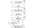
- heat treatment step S04 After the hot working step S03, heat treatment is performed.
- the heat treatment temperature is less than 300 ° C. or the holding time is less than 0.5 hours, recrystallization does not occur sufficiently and the strain in the hot working step S03 remains, and the KAM value. May be high. Further, the crystal grain size may become too small, the area ratio of the crystal in the (100) plane orientation may be low, and the area ratio of the crystal in the (123) plane orientation may be high.
- the heat treatment temperature exceeds 700 ° C. or the holding time exceeds 24 hours the crystal grain size becomes large, and the area ratio of the crystals in the (100) plane orientation may become too high. Therefore, in the present embodiment, it is preferable that the heat treatment temperature is in the range of 300 ° C. or higher and 700 ° C. or lower, and the holding time at the heat treatment temperature is in the range of 0.5 hour or more and 24 hours or less.
- the heat treatment temperature is more preferably 350 ° C. or higher, and more preferably 400 ° C. or higher.
- the heat treatment temperature is more preferably 650 ° C. or lower, and more preferably 600 ° C. or lower.
- the holding time at the heat treatment temperature is more preferably 0.75 hours or more, and even more preferably 1 hour or more.
- the holding time at the heat treatment temperature is more preferably 18 hours or less, and more preferably 12 hours or less.
- the heating rate during the heat treatment by continuous annealing should be 2 ° C./sec or more. Is more preferable, 5 ° C./sec or more is more preferable, and 7 ° C./sec or more is more preferable.
- the temperature lowering rate is preferably 5 ° C./sec or more, more preferably 7 ° C./sec or more, and even more preferably 10 ° C./sec or more.
- the oxygen partial pressure is preferably 10-5 atm or less, more preferably 10-7 atm or less, and more preferably 10-9 atm or less.
- a finishing process may be performed to adjust the strength.
- the processing method is not specified, but in the case of bar material, drawing processing, extrusion processing, etc. can be mentioned. Further, in the case of a bar material, a drawing step may be performed for straightening. The processing conditions are appropriately adjusted so that the tensile strength in the longitudinal direction of the produced copper alloy plastically processed material is 275 MPa or less.
- the copper alloy plastically processed material (copper alloy rod material) according to the present embodiment is produced.
- the Mg content is within the range of more than 10 mass ppm and 100 mass ppm or less, and the content of Mg and S, which is an element that forms a compound, is set. 10 mass ppm or less, P content is 10 mass ppm or less, Se content is 5 mass ppm or less, Te content is 5 mass ppm or less, Sb content is 5 mass ppm or less, Bi content is 5 mass ppm or less, As content is 5 mass ppm or less.
- the mass ratios [Mg] / [S + P + Se + Te + Sb + Bi + As] are Since it is set in the range of 0.6 or more and 50 or less, it is possible to sufficiently improve the heat resistance after processing without excessive solid solution of Mg to reduce the conductivity. Further, since the tensile strength is 275 MPa or less, the workability is excellent and severe plastic working can be performed.
- the heat capacity becomes large.
- the temperature rise can be suppressed by the energization heat generation.
- the workability is particularly excellent, and more severe plastic working can be performed.
- the Ag content is within the range of 5 mass ppm or more and 20 mass ppm or less, Ag segregates in the vicinity of the grain boundaries, and the Ag causes the grain boundaries. Diffusion is suppressed, and it becomes possible to further improve the heat resistance after processing.
- the content of H is 10 mass ppm or less
- the content of O is 100 mass ppm or less
- the content of C is 10 mass ppm or less among the unavoidable impurities, blow. It is possible to reduce the occurrence of defects such as holes, Mg oxides and C entrainment and carbides, and it is possible to improve the heat resistance after processing without deteriorating the workability.
- a measurement area of 10,000 ⁇ m 2 or more is secured in a cross section orthogonal to the longitudinal direction of the copper alloy plastic processed material by the EBSD method and used as an observation surface, and a measurement interval of 0.25 ⁇ m.
- step 1 the orientation difference of each crystal grain is analyzed except for the measurement points whose CI value is 0.1 or less, and the grain boundaries between the measurement points where the orientation difference between adjacent measurement points is 15 ° or more.
- the average grain size A is obtained by Area Fraction, and then measured at a step of a measurement interval that is 1/10 or less of the average grain size A so that a total of 1000 or more crystal grains are contained.
- a measurement area of 10,000 ⁇ m 2 or more is secured in the field of view and used as an observation surface, and the orientation difference of each crystal grain is analyzed except for the measurement points where the CI value analyzed by the data analysis software OIM is 0.1 or less, and adjacent to each other.
- KAM Kernel Age Measurement
- the average value of KAM (Kernel Age Measurement) values when the boundary where the orientation difference between the pixels is 5 ° or more is regarded as the grain boundary is 1.8 or less, it was introduced at the time of processing.
- the region where the density of the rearrangement (GN rearrangement) is high is reduced, the elongation can be ensured, and the workability can be further improved.
- high-speed diffusion of atoms through dislocations can be suppressed, softening phenomena due to recovery and recrystallization can be suppressed, and heat resistance after processing can be further improved.
- the area ratio of the crystals in the (100) plane orientation is 3% or more. (123)
- the area ratio of the crystal in the plane orientation is 70% or less, it is difficult to accumulate dislocations.
- the area ratio of the crystal in the plane orientation is secured at 3% or more, and dislocations are accumulated. Since the area ratio of crystals in the easy (123) plane orientation is limited to 70% or less, elongation can be ensured by suppressing an increase in dislocation density, workability can be further improved, and after processing, the processability can be further improved. The heat resistance can be further improved.
- the crystal grain size of the surface layer region from the outer surface to the center is more than 200 ⁇ m and up to 1000 ⁇ m in the cross section orthogonal to the longitudinal direction of the copper alloy plastic work material.
- the crystal grain size of the surface layer region is 120 ⁇ m or less, the elongation is ensured and the processability can be further improved.
- the copper alloy bar material of the present embodiment is composed of the above-mentioned copper alloy plastically processed material, it can exhibit excellent characteristics even in a large current application and a high temperature environment. Further, since the diameter of the cross section orthogonal to the longitudinal direction of the copper alloy plastic working material is within the range of 3 mm or more and 50 mm or less, sufficient strength and conductivity can be ensured.
- the parts (terminals, etc.) for electronic / electrical equipment according to the present embodiment are made of the above-mentioned copper alloy plastically processed material, they exhibit excellent characteristics even in high current applications and high temperature environments. Can be done.
- the present invention is not limited thereto and deviates from the technical idea of the present invention. It can be changed as appropriate to the extent that it does not.
- an example of a method for manufacturing a copper alloy plastically worked material has been described, but the method for manufacturing a copper alloy plastically worked material is not limited to that described in the embodiment, and is not limited to the existing manufacturing method. The method may be appropriately selected and manufactured.
- the copper raw material was charged into the crucible and melted at high frequency in an atmosphere furnace having an Ar gas atmosphere or an Ar—O 2 gas atmosphere.
- the above-mentioned mother alloy is used to prepare the composition shown in Tables 1 and 2, and when H and O are introduced, the atmosphere at the time of melting is changed to a high-purity Ar gas (dew point -80).
- Ar-N 2 using high-purity N 2 gas (dew point -80 ° C or less), high-purity O 2 gas (dew point -80 ° C or less), and high-purity H 2 gas (dew point -80 ° C or less).
- the atmosphere was a mixed gas atmosphere of —H 2 and Ar—O 2.
- the surface of the molten metal was coated with C particles in the melting and brought into contact with the molten metal.
- the molten alloys having the composition shown in Tables 1 and 2 were melted and poured into a carbon mold to produce ingots.
- the size of the ingot was about 80 mm in diameter and about 300 mm in length.
- the obtained ingot was subjected to a homogenization / solution formation step under the conditions shown in Tables 3 and 4 in an Ar gas atmosphere. Then, hot working (hot extrusion) was performed under the conditions shown in Tables 3 and 4 (working end temperature and extrusion ratio) to obtain a hot work material. After hot working, it was cooled by water cooling.
- the obtained hot-worked material was heat-treated using a salt bath under the conditions shown in Tables 3 and 4, and cooled. Then, the copper material after the heat treatment was cut, and surface grinding was performed to remove the oxide film. Then, finishing processing (cold extrusion processing) was carried out at room temperature under the conditions shown in Tables 3 and 4, to obtain copper alloy plastically processed materials (copper alloy rods) of the examples of the present invention and comparative examples.
- composition analysis A measurement sample was taken from the obtained ingot, Mg was measured by inductively coupled plasma emission spectroscopy, and other elements were measured using a glow discharge mass spectrometer (GD-MS). The analysis of H was performed by the thermal conductivity method, and the analysis of O, S, and C was performed by the infrared absorption method. The measurement was performed at two points, the center of the sample and the end in the width direction, and the one with the higher content was taken as the content of the sample. As a result, it was confirmed that the composition was as shown in Tables 1 and 2.
- the test piece is collected in accordance with the No. 2 test piece specified in JIS Z 2201, and the tensile strength of the copper alloy plastic processed material (copper alloy rod) in the longitudinal direction (extrusion direction) is carried out by the tensile test method of JIS Z 2241. Strength and total elongation were measured. When the cross-sectional area of the cross section orthogonal to the longitudinal direction of the copper alloy plastically worked material exceeds 450 mm 2 , the test was performed with the length of the parallel portion in the longitudinal direction of the copper alloy plastically worked material being 200 mm.
- Tensile strength is the stress corresponding to the maximum tensile test force of the tensile test, and total elongation is the total elongation at fracture (combined elastic elongation and plastic elongation of the extensometer), which is a percentage of the extensometer reference point distance. It is the value shown in.
- the obtained copper alloy plastically processed material (copper alloy bar) was subjected to drawing processing at room temperature with a cross-sectional reduction rate of 25%. Then, according to JCBA T325: 2013 of the Japan Copper and Brass Association, the evaluation was made by acquiring an isochronous softening curve by a tensile test in the longitudinal direction (pulling direction) of the copper alloy plastically processed material after one hour of heat treatment.
- the heat-resistant temperature is the heat treatment temperature at which the strength becomes 0.8 ⁇ T 0 with respect to the strength T 0 before the heat treatment after the heat treatment at 100 to 800 ° C. with a heat treatment time of 60 minutes. ..
- the strength T 0 before the heat treatment is a value measured at room temperature (15 to 35 ° C.).
- conductivity The conductivity was calculated by JIS H 0505 (method for measuring volume resistivity and conductivity of non-ferrous metal materials).
- KAM value The average value of KAM values was obtained as follows by an EBSD measuring device and OIM analysis software, using a cross section orthogonal to the longitudinal direction (drawing direction) of the copper alloy rod (copper alloy plastically worked material) as an observation surface.
- the observation surface was mechanically polished using water-resistant abrasive paper and diamond abrasive grains, and then finish-polished using a colloidal silica solution. Then, the EBSD measuring device (Quanta FEG 450 manufactured by FEI, OIM Data Collection manufactured by EDAX / TSL (currently AMETEK)) and the analysis software (EDAX / TSL (currently AMETEK) OIM Data Analysis ver.7.3). According to 1), observe the observation surface of the electron beam with an acceleration voltage of 15 kV and a measurement area of 10000 ⁇ m 2 or more, and each measurement point has a CI value of 0.1 or less at the step of the measurement interval of 0.25 ⁇ m. The azimuth difference of the crystal grains was analyzed, and the average particle size A by Area Fraction was obtained using the data analysis software OIM, with the azimuth difference between the adjacent measurement points being 15 ° or more as the crystal grain boundary. ..
- the observation surface is measured at a measurement interval step of 1/10 or less of the average particle size A, and the measurement area is 10,000 ⁇ m 2 or more in a plurality of fields so that a total of 1000 or more crystal grains are included.
- Data analysis software OIM analyzed except for the measurement points where the CI value was 0.1 or less, and the boundary where the orientation difference between adjacent pixels was 5 ° or more was regarded as the crystal grain boundary and analyzed.
- the KAM value of the pixel was calculated, and the average value was calculated.
- Crystal grain size in the surface layer region With respect to the obtained copper alloy plastically processed material (copper alloy bar), in a cross section orthogonal to the longitudinal direction (extrusion direction) of the copper alloy plastically worked material, it exceeds 200 ⁇ m from the outer surface to the center to 1000 ⁇ m.
- the average crystal grain size in the surface layer region was measured.
- the average crystal grain size here is the area average crystal grain size. 0 °, 90 °, 180 ° along the circumferential direction from the axis with respect to an arbitrary axis passing through the center of the cross section orthogonal to the above-mentioned average crystal grain size and the longitudinal direction (extrusion direction) of the copper alloy plastic work material.
- the four points at the 270 ° position were measured, and the crystal grain sizes at each of the four points were averaged.
- the measurement was performed using SEM-EBSD (detector HIKARI, analysis software TSL OIM Data collection 5.31 and OIM Analysis 6.2) between measurement points where the orientation difference between two adjacent crystals is 15 ° or more.
- the crystal grain boundary was used, and the weighted average value weighted by the area was used as the crystal grain size.
- the step size was set to 1 ⁇ m.
- Comparative Example 1 since the Mg content was less than the range of the present invention, the heat resistance after processing was insufficient. In Comparative Example 2, the Mg content was beyond the range of the present invention, and the conductivity was low. In Comparative Example 3, the total content of S, P, Se, Te, Sb, Bi, and As exceeded 30 mass ppm, and the heat resistance after processing was insufficient. In Comparative Example 4, the mass ratio [Mg] / [S + P + Se + Te + Sb + Bi + As] was less than 0.6, and the heat resistance after processing was insufficient. In Comparative Example 5, the cross-sectional area reduction rate of the finishing process was too high, so that the strength was beyond the range of the present invention, the total elongation was low, and the processability was inferior. In addition, the heat resistance after processing was insufficient.
- Examples 1 to 22 of the present invention the strength was low, the total elongation was high, and the processability was sufficiently excellent. In addition, the conductivity became high. Furthermore, it was also excellent in heat resistance after processing. From the above, it has been confirmed that according to the example of the present invention, it is possible to provide a copper alloy plastically processed material having high conductivity, excellent workability, and excellent heat resistance even after processing. Was done.
Landscapes
- Chemical & Material Sciences (AREA)
- Engineering & Computer Science (AREA)
- Materials Engineering (AREA)
- Mechanical Engineering (AREA)
- Metallurgy (AREA)
- Organic Chemistry (AREA)
- Physics & Mathematics (AREA)
- Thermal Sciences (AREA)
- Crystallography & Structural Chemistry (AREA)
- Conductive Materials (AREA)
Abstract
Priority Applications (4)
| Application Number | Priority Date | Filing Date | Title |
|---|---|---|---|
| US18/003,416 US20230313341A1 (en) | 2020-06-30 | 2021-06-30 | Copper alloy plastic working material, copper alloy rod material, component for electronic/electrical devices, and terminal |
| CN202180046181.XA CN115735014B (zh) | 2020-06-30 | 2021-06-30 | 铜合金塑性加工材、铜合金棒材、电子电气设备用组件及端子 |
| EP21834589.0A EP4174201A4 (fr) | 2020-06-30 | 2021-06-30 | Matériau de façonnage plastique en alliage de cuivre, matériau de tige en alliage de cuivre, composant pour dispositifs électroniques/électriques, et terminal |
| KR1020227045902A KR20230031230A (ko) | 2020-06-30 | 2021-06-30 | 구리 합금 소성 가공재, 구리 합금 봉재, 전자·전기 기기용 부품, 단자 |
Applications Claiming Priority (6)
| Application Number | Priority Date | Filing Date | Title |
|---|---|---|---|
| JP2020-112927 | 2020-06-30 | ||
| JP2020112927A JP7078070B2 (ja) | 2020-06-30 | 2020-06-30 | 銅合金、銅合金塑性加工材、電子・電気機器用部品、端子、バスバー、リードフレーム |
| JP2020-112695 | 2020-06-30 | ||
| JP2020112695A JP7136157B2 (ja) | 2020-06-30 | 2020-06-30 | 銅合金、銅合金塑性加工材、電子・電気機器用部品、端子 |
| JP2021-091161 | 2021-05-31 | ||
| JP2021091161A JP7205567B2 (ja) | 2021-05-31 | 2021-05-31 | 銅合金塑性加工材、銅合金棒材、電子・電気機器用部品、端子 |
Publications (1)
| Publication Number | Publication Date |
|---|---|
| WO2022004803A1 true WO2022004803A1 (fr) | 2022-01-06 |
Family
ID=79316363
Family Applications (1)
| Application Number | Title | Priority Date | Filing Date |
|---|---|---|---|
| PCT/JP2021/024797 Ceased WO2022004803A1 (fr) | 2020-06-30 | 2021-06-30 | Matériau de façonnage plastique en alliage de cuivre, matériau de tige en alliage de cuivre, composant pour dispositifs électroniques/électriques, et terminal |
Country Status (6)
| Country | Link |
|---|---|
| US (1) | US20230313341A1 (fr) |
| EP (1) | EP4174201A4 (fr) |
| KR (1) | KR20230031230A (fr) |
| CN (1) | CN115735014B (fr) |
| TW (1) | TW202212584A (fr) |
| WO (1) | WO2022004803A1 (fr) |
Cited By (1)
| Publication number | Priority date | Publication date | Assignee | Title |
|---|---|---|---|---|
| EP4467675A4 (fr) * | 2022-07-29 | 2025-12-24 | Mitsubishi Materials Corp | Matériau de cuivre pur, substrat isolant, et dispositif électronique |
Families Citing this family (4)
| Publication number | Priority date | Publication date | Assignee | Title |
|---|---|---|---|---|
| EP4174198A4 (fr) * | 2020-06-30 | 2025-01-15 | Mitsubishi Materials Corporation | Alliage de cuivre, matériau en alliage de cuivre travaillé plastiquement, composant pour appareil électronique ou électrique, borne, barre omnibus, grille de connexion et substrat de dissipation de chaleur |
| EP4174197A4 (fr) * | 2020-06-30 | 2025-01-15 | Mitsubishi Materials Corporation | Matériau de travail en alliage de cuivre/plastique, matériau de fil en alliage de cuivre, composant pour équipement électronique et électrique et borne |
| JP7136157B2 (ja) | 2020-06-30 | 2022-09-13 | 三菱マテリアル株式会社 | 銅合金、銅合金塑性加工材、電子・電気機器用部品、端子 |
| EP4174199B1 (fr) * | 2020-06-30 | 2025-12-03 | Mitsubishi Materials Corporation | Alliage de cuivre, matériau en alliage de cuivre travaillé plastiquement, composant pour appareil électronique ou électrique, borne, barre omnibus, grille de connexion et substrat de dissipation de chaleur |
Citations (9)
| Publication number | Priority date | Publication date | Assignee | Title |
|---|---|---|---|---|
| JPS4915324B1 (fr) * | 1970-03-05 | 1974-04-13 | ||
| JPS5789448A (en) * | 1980-11-21 | 1982-06-03 | Tatsuta Electric Wire & Cable Co Ltd | Copper alloy for conducting electricity |
| JPS5794537A (en) * | 1980-12-01 | 1982-06-12 | Mitsubishi Metal Corp | Cu alloy having high heat resistance and high conductivity |
| US20060198757A1 (en) * | 2003-04-03 | 2006-09-07 | Ilppo Hiekkanen | Oxygen-free copper alloy and method for its manufacture and use of copper alloy |
| JP2016056414A (ja) | 2014-09-10 | 2016-04-21 | 三菱マテリアル株式会社 | 銅圧延板及び電子・電気機器用部品 |
| JP2020112927A (ja) | 2019-01-09 | 2020-07-27 | 株式会社デンソー | 運転支援装置 |
| JP2020112695A (ja) | 2019-01-11 | 2020-07-27 | キヤノン株式会社 | 露光装置、露光方法および、物品製造方法 |
| WO2021107096A1 (fr) * | 2019-11-29 | 2021-06-03 | 三菱マテリアル株式会社 | Alliage de cuivre, matériau en alliage de cuivre travaillé plastiquement, composant pour appareil électronique ou électrique, borne, barre omnibus, et substrat de dissipation de chaleur |
| JP2021091161A (ja) | 2019-12-11 | 2021-06-17 | エルジー ディスプレイ カンパニー リミテッド | フロントカバーフィルム及びその製造方法、並びに画像表示装置 |
Family Cites Families (5)
| Publication number | Priority date | Publication date | Assignee | Title |
|---|---|---|---|---|
| EP2439296B1 (fr) * | 2005-07-07 | 2013-08-28 | Kabushiki Kaisha Kobe Seiko Sho | Alliage de cuivre haute résistance et maniabilité de pliage supérieure, et procédé de fabrication de plaques d'alliage en cuivre |
| JP3838521B1 (ja) * | 2005-12-27 | 2006-10-25 | 株式会社神戸製鋼所 | 高強度および優れた曲げ加工性を備えた銅合金およびその製造方法 |
| JP6248389B2 (ja) * | 2012-12-05 | 2017-12-20 | 三菱マテリアル株式会社 | 電子・電気機器用銅合金、電子・電気機器用部品及び端子 |
| JP5983589B2 (ja) * | 2013-12-11 | 2016-08-31 | 三菱マテリアル株式会社 | 電子・電気機器用銅合金圧延材、電子・電気機器用部品及び端子 |
| EP4174197A4 (fr) * | 2020-06-30 | 2025-01-15 | Mitsubishi Materials Corporation | Matériau de travail en alliage de cuivre/plastique, matériau de fil en alliage de cuivre, composant pour équipement électronique et électrique et borne |
-
2021
- 2021-06-30 TW TW110124081A patent/TW202212584A/zh unknown
- 2021-06-30 WO PCT/JP2021/024797 patent/WO2022004803A1/fr not_active Ceased
- 2021-06-30 CN CN202180046181.XA patent/CN115735014B/zh active Active
- 2021-06-30 US US18/003,416 patent/US20230313341A1/en not_active Abandoned
- 2021-06-30 EP EP21834589.0A patent/EP4174201A4/fr not_active Withdrawn
- 2021-06-30 KR KR1020227045902A patent/KR20230031230A/ko not_active Withdrawn
Patent Citations (9)
| Publication number | Priority date | Publication date | Assignee | Title |
|---|---|---|---|---|
| JPS4915324B1 (fr) * | 1970-03-05 | 1974-04-13 | ||
| JPS5789448A (en) * | 1980-11-21 | 1982-06-03 | Tatsuta Electric Wire & Cable Co Ltd | Copper alloy for conducting electricity |
| JPS5794537A (en) * | 1980-12-01 | 1982-06-12 | Mitsubishi Metal Corp | Cu alloy having high heat resistance and high conductivity |
| US20060198757A1 (en) * | 2003-04-03 | 2006-09-07 | Ilppo Hiekkanen | Oxygen-free copper alloy and method for its manufacture and use of copper alloy |
| JP2016056414A (ja) | 2014-09-10 | 2016-04-21 | 三菱マテリアル株式会社 | 銅圧延板及び電子・電気機器用部品 |
| JP2020112927A (ja) | 2019-01-09 | 2020-07-27 | 株式会社デンソー | 運転支援装置 |
| JP2020112695A (ja) | 2019-01-11 | 2020-07-27 | キヤノン株式会社 | 露光装置、露光方法および、物品製造方法 |
| WO2021107096A1 (fr) * | 2019-11-29 | 2021-06-03 | 三菱マテリアル株式会社 | Alliage de cuivre, matériau en alliage de cuivre travaillé plastiquement, composant pour appareil électronique ou électrique, borne, barre omnibus, et substrat de dissipation de chaleur |
| JP2021091161A (ja) | 2019-12-11 | 2021-06-17 | エルジー ディスプレイ カンパニー リミテッド | フロントカバーフィルム及びその製造方法、並びに画像表示装置 |
Cited By (1)
| Publication number | Priority date | Publication date | Assignee | Title |
|---|---|---|---|---|
| EP4467675A4 (fr) * | 2022-07-29 | 2025-12-24 | Mitsubishi Materials Corp | Matériau de cuivre pur, substrat isolant, et dispositif électronique |
Also Published As
| Publication number | Publication date |
|---|---|
| EP4174201A4 (fr) | 2024-12-25 |
| US20230313341A1 (en) | 2023-10-05 |
| KR20230031230A (ko) | 2023-03-07 |
| CN115735014B (zh) | 2024-01-26 |
| TW202212584A (zh) | 2022-04-01 |
| CN115735014A (zh) | 2023-03-03 |
| EP4174201A1 (fr) | 2023-05-03 |
Similar Documents
| Publication | Publication Date | Title |
|---|---|---|
| JP7380550B2 (ja) | 純銅板 | |
| JP7024925B2 (ja) | 銅合金、銅合金塑性加工材、電子・電気機器用部品、端子、バスバー、放熱基板 | |
| JP6758746B2 (ja) | 電子・電気機器用銅合金、電子・電気機器用銅合金板条材、電子・電気機器用部品、端子、及び、バスバー | |
| JP7342956B2 (ja) | 純銅板 | |
| WO2022004803A1 (fr) | Matériau de façonnage plastique en alliage de cuivre, matériau de tige en alliage de cuivre, composant pour dispositifs électroniques/électriques, et terminal | |
| KR20120130344A (ko) | 전자 재료용 Cu-Ni-Si-Co 계 구리 합금 및 그 제조 방법 | |
| JP6981587B2 (ja) | 銅合金、銅合金塑性加工材、電子・電気機器用部品、端子、バスバー、放熱基板 | |
| EP4174199B1 (fr) | Alliage de cuivre, matériau en alliage de cuivre travaillé plastiquement, composant pour appareil électronique ou électrique, borne, barre omnibus, grille de connexion et substrat de dissipation de chaleur | |
| CN115735013B (zh) | 铜合金塑性加工材、铜合金线材、电子电气设备用组件及端子 | |
| JP7205567B2 (ja) | 銅合金塑性加工材、銅合金棒材、電子・電気機器用部品、端子 | |
| JP7848781B2 (ja) | 銅合金板 | |
| JP7078091B2 (ja) | 銅合金、銅合金塑性加工材、電子・電気機器用部品、端子、バスバー、リードフレーム、放熱基板 | |
| JP7512845B2 (ja) | 銅合金、銅合金塑性加工材、電子・電気機器用部品、端子、バスバー、リードフレーム、放熱基板 | |
| JP7078070B2 (ja) | 銅合金、銅合金塑性加工材、電子・電気機器用部品、端子、バスバー、リードフレーム | |
| WO2023127851A1 (fr) | Matériau de barre déformé en alliage de cuivre, composant pour appareil électronique ou électrique, borne, barre omnibus, grille de connexion, et substrat de dissipation de chaleur | |
| JP7120389B1 (ja) | 銅合金塑性加工材、銅合金線材、電子・電気機器用部品、端子 | |
| CN121909296A (zh) | 铜合金、铜合金塑性加工材料、电子电气设备用部件、柔性器件用部件、散热用部件及金属密封材料 | |
| TW202206611A (zh) | 銅合金、銅合金塑性加工材、電子電氣機器用零件、端子、匯流排、導線框、散熱基板 |
Legal Events
| Date | Code | Title | Description |
|---|---|---|---|
| 121 | Ep: the epo has been informed by wipo that ep was designated in this application |
Ref document number: 21834589 Country of ref document: EP Kind code of ref document: A1 |
|
| WWE | Wipo information: entry into national phase |
Ref document number: 202217075646 Country of ref document: IN |
|
| NENP | Non-entry into the national phase |
Ref country code: DE |
|
| ENP | Entry into the national phase |
Ref document number: 2021834589 Country of ref document: EP Effective date: 20230130 |
|
| WWW | Wipo information: withdrawn in national office |
Ref document number: 2021834589 Country of ref document: EP |