WO2022018873A1 - Dispositif source de tension continue élevée et dispositif à faisceaux de particules chargées - Google Patents
Dispositif source de tension continue élevée et dispositif à faisceaux de particules chargées Download PDFInfo
- Publication number
- WO2022018873A1 WO2022018873A1 PCT/JP2020/028562 JP2020028562W WO2022018873A1 WO 2022018873 A1 WO2022018873 A1 WO 2022018873A1 JP 2020028562 W JP2020028562 W JP 2020028562W WO 2022018873 A1 WO2022018873 A1 WO 2022018873A1
- Authority
- WO
- WIPO (PCT)
- Prior art keywords
- voltage source
- voltage
- high voltage
- variable
- switching circuit
- Prior art date
- Legal status (The legal status is an assumption and is not a legal conclusion. Google has not performed a legal analysis and makes no representation as to the accuracy of the status listed.)
- Ceased
Links
Images






Classifications
-
- H—ELECTRICITY
- H01—ELECTRIC ELEMENTS
- H01J—ELECTRIC DISCHARGE TUBES OR DISCHARGE LAMPS
- H01J37/00—Discharge tubes with provision for introducing objects or material to be exposed to the discharge, e.g. for the purpose of examination or processing thereof
- H01J37/02—Details
- H01J37/248—Components associated with high voltage supply
-
- H—ELECTRICITY
- H02—GENERATION; CONVERSION OR DISTRIBUTION OF ELECTRIC POWER
- H02M—APPARATUS FOR CONVERSION BETWEEN AC AND AC, BETWEEN AC AND DC, OR BETWEEN DC AND DC, AND FOR USE WITH MAINS OR SIMILAR POWER SUPPLY SYSTEMS; CONVERSION OF DC OR AC INPUT POWER INTO SURGE OUTPUT POWER; CONTROL OR REGULATION THEREOF
- H02M7/00—Conversion of AC power input into DC power output; Conversion of DC power input into AC power output
- H02M7/02—Conversion of AC power input into DC power output without possibility of reversal
- H02M7/04—Conversion of AC power input into DC power output without possibility of reversal by static converters
- H02M7/06—Conversion of AC power input into DC power output without possibility of reversal by static converters using discharge tubes without control electrode or semiconductor devices without control electrode
- H02M7/10—Conversion of AC power input into DC power output without possibility of reversal by static converters using discharge tubes without control electrode or semiconductor devices without control electrode arranged for operation in series, e.g. for multiplication of voltage
- H02M7/103—Containing passive elements (capacitively coupled) which are ordered in cascade on one source
-
- H—ELECTRICITY
- H02—GENERATION; CONVERSION OR DISTRIBUTION OF ELECTRIC POWER
- H02M—APPARATUS FOR CONVERSION BETWEEN AC AND AC, BETWEEN AC AND DC, OR BETWEEN DC AND DC, AND FOR USE WITH MAINS OR SIMILAR POWER SUPPLY SYSTEMS; CONVERSION OF DC OR AC INPUT POWER INTO SURGE OUTPUT POWER; CONTROL OR REGULATION THEREOF
- H02M1/00—Details of apparatus for conversion
- H02M1/0043—Converters switched with a phase shift, i.e. interleaved
-
- H—ELECTRICITY
- H02—GENERATION; CONVERSION OR DISTRIBUTION OF ELECTRIC POWER
- H02M—APPARATUS FOR CONVERSION BETWEEN AC AND AC, BETWEEN AC AND DC, OR BETWEEN DC AND DC, AND FOR USE WITH MAINS OR SIMILAR POWER SUPPLY SYSTEMS; CONVERSION OF DC OR AC INPUT POWER INTO SURGE OUTPUT POWER; CONTROL OR REGULATION THEREOF
- H02M1/00—Details of apparatus for conversion
- H02M1/14—Arrangements for reducing ripples from DC input or output
-
- H—ELECTRICITY
- H02—GENERATION; CONVERSION OR DISTRIBUTION OF ELECTRIC POWER
- H02M—APPARATUS FOR CONVERSION BETWEEN AC AND AC, BETWEEN AC AND DC, OR BETWEEN DC AND DC, AND FOR USE WITH MAINS OR SIMILAR POWER SUPPLY SYSTEMS; CONVERSION OF DC OR AC INPUT POWER INTO SURGE OUTPUT POWER; CONTROL OR REGULATION THEREOF
- H02M3/00—Conversion of DC power input into DC power output
- H02M3/02—Conversion of DC power input into DC power output without intermediate conversion into AC
- H02M3/04—Conversion of DC power input into DC power output without intermediate conversion into AC by static converters
- H02M3/06—Conversion of DC power input into DC power output without intermediate conversion into AC by static converters using resistors or capacitors, e.g. potential divider
- H02M3/07—Conversion of DC power input into DC power output without intermediate conversion into AC by static converters using resistors or capacitors, e.g. potential divider using capacitors charged and discharged alternately by semiconductor devices with control electrode, e.g. charge pumps
-
- H—ELECTRICITY
- H02—GENERATION; CONVERSION OR DISTRIBUTION OF ELECTRIC POWER
- H02M—APPARATUS FOR CONVERSION BETWEEN AC AND AC, BETWEEN AC AND DC, OR BETWEEN DC AND DC, AND FOR USE WITH MAINS OR SIMILAR POWER SUPPLY SYSTEMS; CONVERSION OF DC OR AC INPUT POWER INTO SURGE OUTPUT POWER; CONTROL OR REGULATION THEREOF
- H02M3/00—Conversion of DC power input into DC power output
- H02M3/22—Conversion of DC power input into DC power output with intermediate conversion into AC
- H02M3/24—Conversion of DC power input into DC power output with intermediate conversion into AC by static converters
- H02M3/28—Conversion of DC power input into DC power output with intermediate conversion into AC by static converters using discharge tubes with control electrode or semiconductor devices with control electrode to produce the intermediate AC
Definitions
- the present disclosure relates to a DC high voltage source device and a charged particle beam device including a DC high voltage source device.
- the charged particle beam device includes a scanning electron microscope (SEM), a scanning ion microscope (SIM), a focused ion beam (FIB) processing observation device, and a transmission electron microscope (Transometry). : TEM), Scanning Transmission Electron Microscope (STEM) and the like.
- a scanning electron microscope an electron beam is scanned on the surface of a sample, and the generated signal electrons are detected and imaged to perform magnified observation of the sample.
- magnified observation of the sample is performed by scanning the ion beam.
- the focused ion beam processing observation device processing of a sample using an ion beam and magnified observation are carried out.
- magnified observation is performed by forming an image of electrons transmitted through a thin film sample.
- a charged particle beam device using a charged particle beam such as an electron beam or an ion beam is used for observation, length measurement, analysis, processing, etc. of fine structures in various fields. For example, in a semiconductor device manufacturing line, defect observation, analysis, pattern dimension length measurement, etc. are performed using a scanning electron microscope.
- the charged particle beam device is equipped with a charged particle gun for generating and accelerating the charged particle beam.
- the charged particle gun comprises a charged particle source, an extraction electrode, and an acceleration electrode.
- a charged particle beam is generated by applying a DC high voltage of several kV between the charged particle source and the extraction electrode, and several kV to several hundred kV is generated between the extraction electrode and the acceleration electrode.
- the high DC voltage applied between the charged particle source and the accelerating electrode corresponds to the beam energy of the charged particle beam and is the main factor that determines the performance of the charged particle beam device such as image resolution, focal depth, and sample processing speed. It is one of the causes.
- the charged particle beam device is equipped with a DC high voltage source device for generating a DC high voltage applied to the charged particle gun.
- Many DC high voltage source devices for charged particle guns are equipped with a transformer and a Cockcroft-Walton circuit to rectify and boost an AC voltage to a DC voltage. These transformers and Cockcroft-Walton circuits are mounted in insulating resin material, insulating gas, and insulating oil within the size range allowed in the usage environment of the charged particle beam device.
- an AC component (hereinafter, also referred to as “ripple”) is added to the DC high voltage of the output unit due to electrostatic induction noise and electromagnetic induction noise generated by circuit components and wiring to which an AC voltage is applied. Occurs.
- the DC high voltage ripple applied to a charged particle gun is equivalent to energy dispersive. Therefore, the ripple generated in the DC high voltage becomes a factor that lowers the resolution of the charged particle beam device.
- Patent Document 1 provides a Schenkel-type DC high voltage that adjusts the noise balance and completely cancels the ripple by adjusting the stray capacitance between the high-frequency drive electrode and the ground potential portion by providing a distance adjustment mechanism.
- the generation circuit is disclosed.
- Patent Document 2 a voltage source for varying the two opposite-phase AC voltages input to the symmetric Cockcroft-Walton circuit is added in series to the secondary coil of the transformer to provide ripple without moving parts. Techniques for reduction are disclosed.
- the ripple reduction mechanism by movable adjustment can also be applied to the symmetric Cockcroft-Walton circuit.
- Patent Document 1 in order to apply the technique of Patent Document 1 to a circuit mounted in an insulating gas or an insulating oil, it is necessary to adjust a moving part from the outside of the gas container or the oil container, which is extremely difficult. .. Further, in the long term, there is a possibility that the ripple may reoccur due to the displacement of the moving part. Further, a movable portion cannot be provided for a circuit that is molded (fixed) by an insulating resin material.
- Patent Document 2 describes that a ripple measuring circuit is provided and a variable voltage is controlled so that the measured ripple value becomes a desired value.
- this configuration has the following problems. (1) Residual ripple due to waveform mismatch
- Patent Document 2 describes that the variable voltage has the same phase as the voltage waveform excited by the secondary coil of the transformer, and the amplitude is controlled by the voltage adjusting mechanism. The control method is not described.
- the AC voltage supplied to the primary coil of the transformer is generated by turning the switching element on and off with respect to the DC voltage.
- the generated AC voltage becomes a distorted waveform like a sine wave due to the inductance of the primary coil of the transformer.
- the same voltage waveform as the primary coil is excited in the secondary coil of the transformer with different amplitudes, but in order to completely cancel the ripple in the output stage, it is necessary to generate the same voltage waveform in the variable voltage source. There is.
- the present disclosure aims to reduce the ripple generated in the DC high voltage.
- the DC high voltage source apparatus is a first variable DC voltage source, a second variable DC voltage source, and a first variable DC voltage source that generates an AC voltage from the DC voltage of the first variable DC voltage source.
- a DC high voltage is generated based on the second transformer that transforms the AC voltage to be generated, the AC voltage after transformation supplied from the first transformer, and the AC voltage after transformation supplied from the second transformer.
- It is provided with a first voltage source including a DC high voltage generation circuit and a computer system. In the computer system, the voltage value of the DC voltage of the first variable DC voltage source, the voltage value of the DC voltage of the second variable DC voltage source, the switching timing of the first switching circuit, the switching timing of the second switching circuit, and so on. Adjust independently.
- FIG. 1 is a diagram showing an example of the configuration of the DC high voltage source device according to the first embodiment of the present disclosure.
- the DC high voltage source device 205 includes a second voltage source 206 and a first voltage source 207.
- a first voltage source 207 is provided on the upstream side
- a second voltage source 206 is provided on the downstream side
- the second voltage source 206 and the first voltage source 207 are connected in series.
- the positive terminal of the first voltage source 207 is grounded.
- the DC high voltage source device 205 adds the output voltage of the second voltage source 206 to the output voltage of the first voltage source 207, and outputs the added voltage.
- the DC high voltage source device 205 may be composed of only the first voltage source 207.
- FIG. 2 is a circuit block diagram showing an example of the first voltage source.
- the second voltage source 206 may also have the same configuration as the first voltage source 207 described below.
- the first voltage source 207 is a circuit that generates a DC high voltage of several tens of kV to several hundreds of kV.
- the first voltage source 207 includes a first variable DC voltage source 301, a second variable DC voltage source 302, a first switching circuit 303, a second switching circuit 304, a computer system 305, and a first transformer. It includes a 306, a second transformer 307, a DC high voltage generation circuit 308, and a low pass filter 309.
- the DC high voltage source device 205 of the present disclosure is applicable to a product using a DC high voltage generation circuit 308 such as a Cockcroft-Walton circuit.
- the first variable DC voltage source 301 is connected to the input end of the first switching circuit 303.
- the output end of the first switching circuit 303 is connected to the input end of the first transformer 306.
- the output end of the first transformer 306 is connected to the first input end 401 (FIG. 3) of the DC high voltage generation circuit 308.
- the second variable DC voltage source 302 is connected to the input end of the second switching circuit 304.
- the output end of the second switching circuit 304 is connected to the input end of the second transformer 307.
- the output end of the second transformer 307 is connected to the second input end 402 (FIG. 3) of the DC high voltage generation circuit 308.
- the output end of the DC high voltage generation circuit 308 is connected to the input end of the low-pass filter 309.
- the output end of the low-pass filter 309 is connected to the input end of the second voltage source 206.
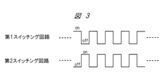
- FIG. 3 is a diagram illustrating the switching timing of the switching circuit.
- the computer system 305 independently and variably controls the voltage value of the first variable DC voltage source 301 and the voltage value of the second variable DC voltage source 302. Further, the computer system 305 independently and variably controls the switching timings of the first switching circuit 303 and the second switching circuit 304. As shown in FIG. 3, the on / off timings of the first switching circuit 303 and the second switching circuit 304 are opposite to each other. That is, when the first voltage source 207 is operating, when the first switching circuit 303 is on, the second switching circuit 304 is off, and when the first switching circuit 303 is off, the second switching circuit 304 is on. There is. In FIG.
- the computer system 305 controls the voltage values of the first variable DC voltage source 301 and the second variable DC voltage source 302, and the voltage of the AC waveform input to the corresponding first transformer 306 and second transformer 307. Can be controlled. Further, the computer system 305 can control the phase of the AC waveform by controlling the switching timing of the first switching circuit 303 and the second switching circuit 304.
- Patent Document 2 another voltage waveform is added in order to adjust the voltage of the voltage waveform of the transformer secondary coil, but it is adjusted in order to completely cancel the noise of the DC high voltage.
- the voltage waveform and the added voltage waveform must match.
- the control of the voltage value of the first variable DC voltage source 301 and the voltage value of the second variable DC voltage source 302 by the computer system 305, and the switching timing control of the first switching circuit 303 and the second switching circuit 304 are, for example, DC high. It is performed based on the measurement result of ripple by the ripple measuring device provided outside the voltage source device 205. If the ripple is measured in the DC high voltage source device 205 or in the vicinity of the DC high voltage source device 205, noise is superimposed on the measurement circuit as described above, and the ripple cannot be measured accurately. Therefore, it is desirable that the ripple measurement be performed by an external device.
- the computer system 305 may be configured by, for example, FPGA (Field Programmable Gate Array) or ASIC (Application Specific Integrated Circuit).
- FPGA Field Programmable Gate Array
- ASIC Application Specific Integrated Circuit
- the AC voltage generated by the switching control of the first switching circuit 303 and the second switching circuit 304 is boosted in the first transformer 306 and the second transformer 307, respectively, and then in the DC high voltage generation circuit 308. Is generated.
- the low-pass filter 309 is composed of, for example, a resistor and a capacitor, reduces the ripple of the output (DC high voltage) of the DC high voltage generation circuit 308, and outputs the DC high voltage with the ripple reduced.
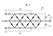
- FIG. 4 is a circuit diagram showing an example of a DC high voltage generation circuit.
- a symmetric Cockcroft-Walton circuit is exemplified as the DC high voltage generation circuit 308.
- the AC voltage from the first transformer 306 AC voltage from the first switching circuit 303
- the AC voltage from the second transformer 307 second
- the AC voltage from the switching circuit 304 is input to the second input terminal 402.
- the symmetric Cockcroft-Walton circuit is a two-input DC high voltage generation circuit.
- the symmetric Cockcroft-Walton circuit has a capacitor and diode arrangement between the first input end 401 and the output end 405 and a capacitor and diode between the second input end 402 and the output end 405, as shown in FIG.
- the arrangement of the diodes is symmetrical.
- FIG. 5 is a circuit diagram showing another example of the DC high voltage generation circuit.
- a basic Cockcroft-Walton circuit is exemplified as a DC high voltage generation circuit 308.
- the basic Cockcroft-Walton circuit shown in FIG. 5 is a one-input DC high voltage generation circuit in which the circuit on the second input end 402 side is deleted from the symmetric Cockcroft-Walton circuit of FIG.
- the second input end 402 is connected to the wiring (signal line) 501, but is not connected to the output end 405.
- the second input end 402 side of the DC high voltage generation circuit 308 is driven by an AC voltage having a phase opposite to that of the first input end 401, similar to the symmetric Cockcroft-Walton circuit.
- the noise at the output end 405 is canceled by the stray capacitance 407 between the wiring 501 and the output end 405, and the ripple is reduced.
- the computer system 305 can independently control the voltage and phase of the two opposite-phase AC voltages input to the Cockcroft-Walton circuit while maintaining the waveform shape. It is possible to significantly reduce the noise of DC high voltage as compared with the conventional case. ⁇ Other examples of DC high voltage generation circuit >>
- the DC high voltage generation circuit 308 is composed of a plurality of diodes and a plurality of capacitors, and is a two-input rectifier in which an AC voltage generated by the first switching circuit 303 and an AC voltage generated by the second switching circuit 304 are input. It may be composed of a circuit.
- the DC high voltage generation circuit is composed of a 2-input Schenkel type DC high voltage generation circuit in which an AC voltage generated by the first switching circuit 303 and an AC voltage generated by the second switching circuit 304 are input. You may. Even in these configurations, it is possible to reduce the ripple while generating a high voltage. ⁇ Other configurations>
- a first amplifier circuit and a second amplifier circuit may be provided in place of the first switching circuit 303 and the second switching circuit 304.
- the first amplifier circuit and the second amplifier circuit amplify the AC signal from the computer system 305 and supply the amplified AC signal to the first transformer and the second transformer, respectively.
- the AC voltage output by the first amplifier circuit and the second amplifier circuit may be directly supplied to the DC high voltage generation circuit 308 without providing the first transformer 306 and the second transformer 307. .. Even in these configurations, it is possible to reduce the ripple while generating a high voltage.
- the first variable DC voltage source 301 and the second variable DC voltage source 302 can be omitted. Then, the computer system 305 adjusts the voltage (amplitude) and the phase of the AC voltage based on the measurement result of the ripple. ⁇ Main effects of this embodiment>
- the computer system 305 switches the DC voltage value of the first variable DC voltage source 301, the DC voltage value of the second variable DC voltage source 302, and the first switching circuit 303.
- the timing and the switching timing of the second switching circuit 304 are adjusted independently. According to this configuration, it is possible to reduce the ripple generated in the DC high voltage.
- the DC high voltage generation circuit is composed of a two-input symmetric Cockcroft-Walton circuit. According to this configuration, since the circuit configuration from the input end to the output end is symmetrical between the input ends, it becomes easy to reduce the ripple while obtaining a high voltage.
- the computer system 305 controls the voltage value of the first variable DC voltage source 301 and the voltage value of the second variable DC voltage source 302, and controls the switching of the first switching circuit 303 and the second switching circuit 304. By doing so, it is possible to reduce the ripple of the DC high voltage including the electrostatic induction noise.
- the ripple can be reduced by adjusting each AC voltage input to the DC high voltage generation circuit 308, so that the low-pass filter 309 can be omitted. This makes it possible to improve the responsiveness of the DC high voltage source device 205.
- the DC high voltage generation circuit 308 is composed of a 1-input basic Cockcroft-Walton circuit. At this time, the DC high voltage generation circuit 308 includes an input end to which the AC voltage generated by the second switching circuit 304 is input, and a wiring 501 connected to the input end and electrostatically coupled to the output end. According to this configuration, it is possible to reduce the ripple of the DC high voltage while simplifying the configuration of the DC high voltage generation circuit 308.
- Surge current / voltage may be generated in the secondary coil of the transformer and the parts of the Cockcroft-Walton circuit when the DC high voltage is discharged. Therefore, adding a variable voltage source in series with the secondary coil of the transformer may lead to an increase in the risk of failure due to discharge.
- the first switching circuit 303 is provided between the first transformer 306 and the first transformer 306. Further, a second switching circuit 304 is provided between the second variable DC voltage source 302 and the second transformer 307. As described above, by providing the variable DC voltage source and the switching circuit on the primary coil side of the transformer in which the discharge surge does not easily go around, it is possible to reduce the risk of failure. [Modification example]
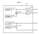
- FIG. 6 is a circuit block diagram showing an example of a configuration of a computer system according to a modified example of the first embodiment of the present disclosure.
- the computer system 305 of FIG. 6 includes a digital multiplier 603, a first digital-analog converter 605 corresponding to a first variable DC voltage source 301, and a second digital-analog converter 606 corresponding to a second variable DC voltage source 302. , A phase shifter 608 is provided.
- the computer system 305 in this variant example may be composed of a digital circuit such as FPGA, ASIC, DSP (Digital Signal Processor), or may include an analog multiplier or a delay circuit at least in part.
- a digital circuit such as FPGA, ASIC, DSP (Digital Signal Processor), or may include an analog multiplier or a delay circuit at least in part.
- the computer system 305 is set with a control signal 601 and a voltage adjustment ratio 602 for controlling the voltage value of the first variable DC voltage source 301, respectively, according to the output DC high voltage.
- the control signal 601 is a signal that defines the voltage of the first variable DC voltage source 301
- the voltage adjustment ratio 602 is the ratio of the voltage of the second variable DC voltage source 302 to the first variable DC voltage source 301. It is a value shown.
- the control signal 601 and the voltage adjustment ratio 602 may be input from the outside or may be generated inside the computer system 305 based on the input signals.
- the control signal 601 is converted into an analog signal by the first digital-analog converter 605.
- the voltage of the first variable DC voltage source 301 is controlled (adjusted).
- the digital multiplier 603 multiplies the control signal 601 and the voltage adjustment ratio 602.
- the multiplication value is converted into an analog signal by the second digital-to-analog converter 606.
- the voltage of the second variable DC voltage source 302 is controlled (adjusted).
- the control signal 601 defines the voltage of the second variable DC voltage source 302, and the voltage adjustment ratio 602 is defined as a value indicating the ratio of the voltage of the first variable DC voltage source 301 to the second variable DC voltage source 302.
- the multiplication value of the digital multiplier 603 may be input to the first variable DC voltage source 301.
- a periodic pulse waveform 607 and a delay time 609 that control the switching timing of the first switching circuit 303 are set according to the output DC high voltage, respectively.
- the delay time 609 is a value that defines the time difference in the switching timing of the second variable DC voltage source 302 with respect to the first variable DC voltage source 301.
- the pulse waveform 607 and the delay time 609 may be input from the outside or may be generated inside the computer system 305 based on the input signal.
- the pulse waveform 607 is supplied to the first switching circuit 303.
- the switching timing of the first switching circuit 303 is adjusted, and the phase of the AC voltage input to the first transformer 306 is adjusted.
- the phase shifter 608 can adjust the switching timing of the second switching circuit 304 by giving a delay to the pulse waveform 607 based on the delay time 609, and can shift the phase of the pulse waveform 607 by a predetermined value. ..
- the phase-shifted pulse waveform 607 is supplied to the second switching circuit 304. As a result, the phase of the AC voltage input to the second transformer 307 is controlled.
- the phase shifter may be provided only on the first switching circuit 303 side, or the phase shifter may be provided on both the first switching circuit 303 side and the second switching circuit 304 side.
- the above-mentioned effects can be obtained.
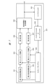
- FIG. 7 is a circuit block diagram showing an example of the first voltage source according to the second embodiment of the present disclosure.
- the first voltage source 207 of FIG. 7 has a configuration in which the low-pass filter 309 is deleted and the high-pass filter 801 and the band-pass filter 802 are added to FIG. 2.
- a high-pass filter 801 and a band-pass filter 802 are connected in series between the output end of the DC high voltage generation circuit 308 and the computer system 305.
- the bandpass filter 802 may be a lowpass filter. However, a low-pass filter with a sufficiently high cutoff frequency is used in order to realize responsiveness that can follow the voltage fluctuation of the partial discharge.
- the input end of the high-pass filter 801 is connected to the output end of the DC high voltage generation circuit 308.
- the output end of the high-pass filter 801 is connected to the input end of the band-pass filter 802.
- the output end of the bandpass filter 802 is connected to the input end of the computer system 305. Therefore, the first voltage source 207 of the present embodiment is configured to output the DC high voltage generated by the DC high voltage generation circuit 308 as it is.
- the high-pass filter 801 is composed of, for example, a capacitor and a resistor.
- the high-pass filter 801 detects an AC component with a high DC voltage.
- This AC component mainly contains a voltage fluctuation component due to partial discharge and a ripple component having a drive frequency of the Cockcroft-Walton circuit, but the ripple component is removed via a bandpass filter 802 or a lowpass filter. Only the voltage fluctuation component mainly due to the partial discharge is input to the computer system 305.
- the computer system 305 controls the voltages of the first variable DC voltage source 301 and the second variable DC voltage source 302 by, for example, changing the control signal 601 of FIG. 6 so as to correct the voltage fluctuation due to the partial discharge.
- the ripple is hardly generated by the voltage and phase control by the computer system 305, but the feedback for correcting the voltage fluctuation due to the partial discharge is not assumed, so that the low-pass filter 309 is provided. ..
- the low-pass filter 309 is provided. ..
- by eliminating the low-pass filter it is possible to realize high-speed responsiveness that follows the voltage fluctuation of the partial discharge while suppressing the generation of ripple.
- FIG. 8 is a diagram showing an example of the configuration of the charged particle beam device according to the third embodiment of the present disclosure.
- a scanning electron microscope will be described as an example as a charged particle beam device.
- a DC high voltage source device is used to generate the charged particle beam (103).
- Charged particles include, for example, electrons and ions.
- the scanning electron microscope 10 includes an electron gun (charged particle gun) 201, a condenser lens 104 which is a form of a focusing lens, a scanning deflector 105, an objective lens 106, a vacuum sample chamber 107, and a conversion electrode 112. , The detector 113, a computer system (charged particle beam device computer system) 120, and the like.
- the electron gun 201 includes an electron source 101, an extraction electrode 102, and the like, and irradiates the sample 109 with the electron beam 103 by the DC high voltage supplied from the DC high voltage source device 205.
- the configuration of the electron gun 201 will be described in detail later.
- the electron beam 103 is drawn from the electron source 101 by the extraction electrode 102, and is accelerated toward the sample 109 by an acceleration electrode (not shown).
- the electron beam 103 is focused by the condenser lens 104, then focused by the lens action of the objective lens 106, and irradiated to the sample 109.
- the electron beam 103 scans the sample 109 one-dimensionally or two-dimensionally by controlling the direction of the beam by the scanning deflector 105.
- the electron beam 103 is decelerated by a voltage applied to an electrode (not shown) built in the sample stage 108 before reaching the sample 109.
- a voltage applied to an electrode for example, in the case of electrons, a negative voltage is applied to the electrodes of the sample stage 108.
- electrons 110 including secondary electrons and backscattered electrons are emitted from the beam irradiation location.
- the electron 110 is accelerated toward the electron source 101 by an accelerating action based on the voltage applied to the sample 109.
- the secondary electrons 111 are emitted.
- the secondary electrons 111 emitted from the conversion electrode 112 are captured by the detector 113, and the output of the detector 113 changes depending on the amount of the captured secondary electrons.
- the brightness of the display device (not shown) changes according to this output.
- an image of a scanning region is formed by synchronizing the deflection signal to the scanning deflector 105 with the output of the detector 113.
- the scanning deflector 105 may be supplied with the deflection signal for moving the field of view superimposed.
- the deflection of the electron beam by the deflection signal is also called image shift deflection, and enables the movement of the visual field position of the electron microscope without moving the sample 109 by the sample stage 108.
- image shift deflection and the scanning deflection are performed by a common deflector, but the image shift deflector and the scanning deflector may be provided separately.
- the computer system 120 is formed on a sample based on, for example, a function of controlling each component of the scanning electron microscope 10, a function of forming an image based on the detected electrons, and an intensity distribution of the detected electrons called a line profile. It has a function to measure the pattern width of the created pattern.
- the computer system 120 controls the applied voltage to the sample 109 or the sample stage 108 and controls the scanning electron microscope 10 based on the monitoring result of the pressure gauge 130 provided in the electrostatic chuck in the vacuum sample chamber 107. To execute or interrupt the measurement.
- the computer system 120 includes a computer system that evaluates an image generated based on a detection signal, and each arithmetic process is executed in the computer system.
- the computer system for evaluating the image may be provided separately from the computer system for performing various controls of the scanning electron microscope 10.
- This program includes a program for driving each component of the scanning electron microscope 10, a program for executing the flow of FIGS. 10 and 11 described later, and the like. Further, this storage medium may store a program to be executed by the computer system 305 of the DC high voltage source device 205. The computer system 305 may store a program to be executed by itself. Further, these storage media may be provided separately from the computer systems 120 and 305.
- FIG. 9 is a diagram illustrating the connection relationship between the electron gun and the DC high voltage source device in the second embodiment of the present disclosure.
- the electron gun 201 and the DC high voltage source device 205 are connected to each other via a connection cable CAB.
- the electron gun 201 is connected to the output end of the DC high voltage source device 205 via a connection cable CAB.
- the electron gun 201 is, for example, a cold cathode field emission type (Cold Field Emission) electron gun.
- the DC high voltage source device 205 is mounted on either an insulating gas, an insulating oil, or an insulating resin material. Since the insulating power of the DC high voltage source device 205 can be improved by using the insulating material, the DC high voltage source device 205 can be miniaturized. By reducing the size of the DC high voltage source device 205, electrostatic coupling and noise superposition may easily occur. However, for each input system of the DC high voltage generation circuit 308, a variable DC voltage source can be used. Since the voltage and the switching timing of the switching circuit can be adjusted respectively, there is no effect on the control of ripple reduction.
- the electron gun 201 includes an electron source 101 as an electron emitter, an extraction electrode 102, and an acceleration electrode 204.
- the electron source 101 is connected to the output end of the second voltage source 206 via the wiring 209, and the DC high voltage generated by the DC high voltage source device 205 is supplied to the electron source 101.
- the first enclosure 210 is provided so as to cover the second voltage source 206, the current source 208, the wiring 209, and the electron source 101. Further, as shown in FIG. 9, the first enclosure 210 connects the output end of the first voltage source 207 and the extraction electrode 102.
- the second enclosure 211 is provided so as to cover the first voltage source 207 and the first enclosure 210. That is, the second enclosure 211 has the function of the housing of the DC high voltage source device 205.
- the second enclosure 211 ie, the enclosure
- the second enclosure 211 is grounded and connects the accelerating electrode 204 to the ground. As a result, the potential of the accelerating electrode 204 is set to the reference potential of the first voltage source 207 (ground potential in FIG. 9).
- an applied voltage is generated between the accelerating electrode 204 and the extraction electrode 102, and an applied voltage between the extraction electrode 102 and the electron source 101 is generated by the second voltage source 206 superimposed on this voltage.
- the first voltage source 207 generates an applied voltage between the acceleration electrode 204 and the electron source 101, and the second voltage source 206 superimposed on this voltage causes the electron source 101 and the extraction electrode 102. It is also possible to generate an applied voltage between. In either configuration, the second voltage source 206 produces a DC high voltage of several kV, and the first voltage source 207 produces a DC high voltage of several tens to several hundreds kV.
- two wirings 209 are connected to the output end of the second voltage source 206, and a current source 208 is provided in one of them.
- the current source 208 is connected in series to the output end of the second voltage source 206, and supplies a current for cleaning the electron source 101 contaminated with particles or the like to the electron source 101 via the wiring 209.
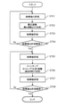
- FIG. 10 is a flow chart showing an example of the ripple reduction method.
- FIG. 10 includes steps S701 to S708. Steps S701 to S704 are steps related to voltage adjustment, and steps S705 to S708 are steps related to phase adjustment.
- step S701 the computer system 120 of FIG. 8 evaluates the ripple based on the acquired index value.
- the index value for example, the resolution of the SEM image (inspection image), the amount of beam sway synchronized with the switching frequency, and the like are used as the index value.
- the output of the DC high voltage source device 205 may be connected to a ripple measuring device outside the device, and the ripple measured value directly measured by the ripple measuring device may be used as an index value. At the time of acquisition of any index value, the measurement system provided inside the DC high voltage source device is not used.
- step S702 the voltages of the first variable DC voltage source 301 and the second variable DC voltage source 302 are adjusted based on the evaluation result of the ripple by the evaluation of the index value in step S701.
- the computer system 120 generates voltage adjustment information of the first variable DC voltage source 301 and the second variable DC voltage source 302 based on the evaluation result of ripple, and outputs the voltage adjustment information to the computer system 305.
- the computer system 305 generates voltage adjustment signals for adjusting the voltages of the first variable DC voltage source 301 and the second variable DC voltage source 302 based on the input voltage adjustment information, and generates the generated voltage adjustment signals. 1 Outputs to the variable DC voltage source 301 and the second variable DC voltage source 302, respectively.
- the computer system 120 when the computer system 305 has the configuration shown in FIG. 6, the computer system 120 generates the control signal 601 and the voltage adjustment ratio 602 of FIG. 6 based on the evaluation result of the index value, and outputs the control signal 601 and the voltage adjustment ratio 602 to the computer system 305.
- the computer system 305 generates a voltage adjustment signal of an analog signal based on the input control signal 601 and the voltage adjustment ratio 602, respectively, and the generated voltage adjustment signal is used as the first variable DC voltage source 301 and the second variable DC voltage source. Output to 302 respectively.
- the voltage may be adjusted by changing only the voltage adjustment ratio 602 without changing the control signal 601.
- step S703 the ripple is evaluated by the index value acquired after the voltage adjustment in step S702. Since the process of step S703 is the same as that of step S701, the details will be omitted.
- step S704 it is determined whether or not the index value is within the allowable range based on the evaluation result in step S703. If the index value is within the permissible range (Yes), the process of step S705 is executed. On the other hand, if the index value is not within the permissible range (No), the process returns to step S701 and the processes of steps S701 to S704 are executed again. That is, if the index value is not within the permissible range, the voltage adjustment ratio 602 and the like are adjusted again.
- the index value may not be within the permissible range.
- the allowable range may be temporarily relaxed to shift to the step of adjusting the phase without delay.
- step S705 the ripple is evaluated by the index value.
- the index value evaluated here is, for example, the value acquired in the immediately preceding step S703.
- the index value is evaluated again from the viewpoint of phase adjustment.
- step S706 the voltage is supplied to the switching timings of the first switching circuit 303 and the second switching circuit 304 based on the evaluation result of the ripple by the evaluation of the index value in step S705, that is, the first transformer 306 and the second transformer 307.
- the phase of the AC voltage is adjusted.
- the computer system 120 generates switching timing adjustment information of the first switching circuit 303 and the second switching circuit 304 based on the evaluation result of the index value, and outputs the switching timing adjustment information to the computer system 305.
- the computer system 305 generates each switching timing adjustment signal for adjusting the switching timing of the first switching circuit 303 and the second switching circuit 304 based on the input switching timing adjustment information, and the generated switching timing adjustment signal is the first. Output to 1 switching circuit 303 and 2nd switching circuit 304, respectively.
- the computer system 120 when the computer system 305 has the configuration of FIG. 6, the computer system 120 generates the delay time 609 of FIG. 6 based on the evaluation result of the index value and outputs it to the computer system 305.
- the computer system 305 generates a phase adjustment signal based on the input delay time 609, and outputs the generated phase adjustment signal to the phase shifter 608.
- the phase may be adjusted by changing only the delay time of the second switching circuit 304 without changing the pulse waveform 607.
- the computer system When a phase shifter is provided at the connection node with the first switching circuit 303, the computer system generates a phase adjustment signal for each phase shifter.
- step S707 the ripple is evaluated by the index value acquired after the phase adjustment in step S706. Since the process of step S707 is the same as that of step S705, the details will be omitted.
- step S708 it is determined whether or not the index value is within the allowable range based on the evaluation result in step S707. If the index value is within the allowable range (Yes), the ripple adjustment is completed. On the other hand, if the index value is not within the permissible range (No), the process returns to step S705, and the processes of steps S705 to S708 are executed again. That is, if the index value is not within the allowable range, the delay time 609 will be adjusted again. ⁇ Ripple reduction method (2)>
- FIG. 11 is a flow chart showing another example of the ripple reduction method.
- step S709 is added to FIG. 10, and the flow is such that the voltage can be adjusted after the voltage is adjusted and the phase is adjusted.
- step S709 after adjusting the phase, it is determined whether or not the voltage readjustment is necessary. Whether or not to readjust the voltage may be selected by the user, or may be automatically determined, for example, by whether or not the index value after the phase adjustment is within a predetermined range. In this case, if the index value after the phase adjustment is not within a predetermined range, it is determined that the voltage needs to be readjusted (No). On the other hand, if the index value after the phase adjustment is within a predetermined range, it is determined that the voltage readjustment is not necessary (Yes).
- FIGS. 10 and 11 show the case where the phase is adjusted after the voltage is adjusted, the voltage may be adjusted after the phase is adjusted. In this case, in step S709 of FIG. 11, it is determined whether or not the phase readjustment is necessary. ⁇ Main effects of this embodiment>
- the DC high voltage source device 205 is connected to the electron gun 201, and the DC high voltage is used for electron irradiation. According to this configuration, it is possible to irradiate a high-quality electron beam with reduced ripple, and it is possible to improve the resolution in the inspection image.
- the computer system 120 generates voltage adjustment information of the first variable DC voltage source 301 and the second variable DC voltage source 302 based on the evaluation result of ripple, and outputs the voltage adjustment information to the computer system 305. do.
- the ripple can be evaluated without superimposing noise on the DC high voltage source device 205. This makes it possible to reduce the ripple more reliably.
- the computer system 120 generates switching timing adjustment information of the first switching circuit 303 and the second switching circuit 304 based on the evaluation result of the ripple, and outputs the switching timing adjustment information to the computer system 305.
- the ripple can be evaluated without superimposing noise on the DC high voltage source device 205. This makes it possible to reduce the ripple more reliably.
- the index value is the resolution of the inspection image or the beam fluctuation amount synchronized with the switching frequency of the first switching circuit 303 or the second switching circuit 304. According to this configuration, the ripple can be evaluated without superimposing noise on the DC high voltage source device 205. This makes it possible to reduce the ripple more reliably.
- the voltage adjustment ratio 602 and the delay time 609 are relative values. Therefore, even if the voltage value of the DC high voltage changes and the control signal 601 that controls the voltage value of the first variable DC voltage source 301 changes, ripple occurs without readjusting the voltage adjustment ratio 602 and the delay time 609. Can be reduced. Further, when the purpose is to reduce the machine difference between the devices, the voltage adjustment ratio 602 and the delay time 609 may be adjusted so as to be aligned with other devices, instead of setting each index value to the optimum value.
- ripple for example, the index value of the SEM image and the measurement system outside the voltage source device are used to compensate according to the adjustment flowchart, and the target of this feedback system is limited to the voltage fluctuation of the partial discharge. Therefore, the voltage fluctuation can be reduced with higher accuracy.
- the present disclosure is not limited to the above-described embodiment, and includes various modifications.
- the cold cathode field emission type electron gun has been described as an example, but the present disclosure can also be applied to other electron guns and ion guns such as thermal electron guns and shotkey electron guns. be.
- the control method and configuration of the present disclosure can be applied not only to an electron gun but also to a component of a charged particle beam lens barrel (column), a voltage supply to a data stage, and a DC high voltage source for an electrostatic chuck. ..
- each member and the relative size described in the drawings are simplified and idealized in order to explain the present disclosure in an easy-to-understand manner, and may have a more complicated shape in mounting.
Landscapes
- Engineering & Computer Science (AREA)
- Power Engineering (AREA)
- Chemical & Material Sciences (AREA)
- Analytical Chemistry (AREA)
- Electron Sources, Ion Sources (AREA)
- Dc-Dc Converters (AREA)
- Particle Accelerators (AREA)
Abstract
Priority Applications (4)
| Application Number | Priority Date | Filing Date | Title |
|---|---|---|---|
| US18/016,989 US12525883B2 (en) | 2020-07-22 | 2020-07-22 | DC high-voltage source device including plurality of variable DC voltage sources and plurality of switching circuits, and charged particle beam device including the DC high-voltage source device |
| JP2022538563A JP7519442B2 (ja) | 2020-07-22 | 2020-07-22 | 直流高電圧源装置および荷電粒子ビーム装置 |
| PCT/JP2020/028562 WO2022018873A1 (fr) | 2020-07-22 | 2020-07-22 | Dispositif source de tension continue élevée et dispositif à faisceaux de particules chargées |
| GB2300708.1A GB2611697B (en) | 2020-07-22 | 2020-07-22 | DC high-voltage source device and charged particle beam device |
Applications Claiming Priority (1)
| Application Number | Priority Date | Filing Date | Title |
|---|---|---|---|
| PCT/JP2020/028562 WO2022018873A1 (fr) | 2020-07-22 | 2020-07-22 | Dispositif source de tension continue élevée et dispositif à faisceaux de particules chargées |
Publications (1)
| Publication Number | Publication Date |
|---|---|
| WO2022018873A1 true WO2022018873A1 (fr) | 2022-01-27 |
Family
ID=79729372
Family Applications (1)
| Application Number | Title | Priority Date | Filing Date |
|---|---|---|---|
| PCT/JP2020/028562 Ceased WO2022018873A1 (fr) | 2020-07-22 | 2020-07-22 | Dispositif source de tension continue élevée et dispositif à faisceaux de particules chargées |
Country Status (4)
| Country | Link |
|---|---|
| US (1) | US12525883B2 (fr) |
| JP (1) | JP7519442B2 (fr) |
| GB (1) | GB2611697B (fr) |
| WO (1) | WO2022018873A1 (fr) |
Families Citing this family (1)
| Publication number | Priority date | Publication date | Assignee | Title |
|---|---|---|---|---|
| WO2021117226A1 (fr) * | 2019-12-13 | 2021-06-17 | 株式会社日立ハイテク | Canon à particules chargées et dispositif à faisceau de particules chargées |
Citations (8)
| Publication number | Priority date | Publication date | Assignee | Title |
|---|---|---|---|---|
| JPH0670492U (ja) * | 1993-03-10 | 1994-09-30 | 日新ハイボルテージ株式会社 | 不平衡シェンケル型直流高電圧発生装置 |
| JP2004135363A (ja) * | 2002-10-08 | 2004-04-30 | A & D Co Ltd | 高出力高電圧電源 |
| JP2005294004A (ja) * | 2004-03-31 | 2005-10-20 | Sunx Ltd | 除電装置 |
| JP2007037268A (ja) * | 2005-07-26 | 2007-02-08 | Nhv Corporation | 直流高圧電源装置およびその運転方法 |
| JP2007236099A (ja) * | 2006-03-01 | 2007-09-13 | Jeol Ltd | 直流高電圧発生装置 |
| JP2008269915A (ja) * | 2007-04-19 | 2008-11-06 | Futex Co Ltd | 高電圧電源装置及びその耐放電性確保方法 |
| JP2012155857A (ja) * | 2011-01-21 | 2012-08-16 | Keyence Corp | 除電器 |
| JP2017158277A (ja) * | 2016-03-01 | 2017-09-07 | Smc株式会社 | 高電圧発生回路 |
Family Cites Families (35)
| Publication number | Priority date | Publication date | Assignee | Title |
|---|---|---|---|---|
| US3484866A (en) * | 1967-04-26 | 1969-12-16 | Nippon Electron Optics Lab | Direct current high voltage generator |
| FR2085193B1 (fr) * | 1970-01-16 | 1974-09-20 | Automatisme Cie Gle | |
| US3731145A (en) * | 1970-11-23 | 1973-05-01 | Nordson Corp | Electrostatic spray gun with self-contained miniaturized power pack integral therewith |
| JPS6028232B2 (ja) * | 1975-08-14 | 1985-07-03 | シャープ株式会社 | Dc−dcコンバ−タ |
| US4050005A (en) * | 1976-05-27 | 1977-09-20 | Biometrics Instrument Corporation | Dual phase input multiplier |
| US4745520A (en) * | 1986-10-10 | 1988-05-17 | Ransburg Corporation | Power supply |
| JPS63153788U (fr) | 1987-03-04 | 1988-10-07 | ||
| US4893227A (en) * | 1988-07-08 | 1990-01-09 | Venus Scientific, Inc. | Push pull resonant flyback switchmode power supply converter |
| US5008800A (en) * | 1990-03-02 | 1991-04-16 | Science Research Laboratory, Inc. | High voltage power supply |
| JPH0670492A (ja) * | 1992-08-18 | 1994-03-11 | Matsushita Electric Ind Co Ltd | モータのロータコア |
| JPH11225476A (ja) | 1998-02-06 | 1999-08-17 | Nissin High Voltage Co Ltd | 直流高圧電源装置 |
| US6519168B2 (en) * | 2000-07-24 | 2003-02-11 | Chippower.Com, Inc. | High frequency DC to AC inverter |
| US6927985B2 (en) * | 2001-07-17 | 2005-08-09 | Newton Scientific, Inc. | High voltage generator |
| US7583521B2 (en) * | 2006-02-23 | 2009-09-01 | American Power Conversion Corporation | Over voltage clamp |
| WO2008050540A1 (fr) * | 2006-10-25 | 2008-05-02 | Hitachi Medical Corporation | Générateur de rayons x |
| US7974106B2 (en) * | 2007-05-07 | 2011-07-05 | Bloom Energy Corporation | Ripple cancellation |
| US7839023B2 (en) * | 2007-07-18 | 2010-11-23 | Raytheon Company | Methods and apparatus for three-phase inverter with reduced energy storage |
| JP5231038B2 (ja) * | 2008-02-18 | 2013-07-10 | 東京エレクトロン株式会社 | プラズマ処理装置およびプラズマ処理方法、ならびに記憶媒体 |
| US8723452B2 (en) * | 2010-12-08 | 2014-05-13 | Gtat Corporation | D.C. charged particle accelerator and a method of accelerating charged particles |
| US8558486B2 (en) * | 2010-12-08 | 2013-10-15 | Gtat Corporation | D. c. Charged particle accelerator, a method of accelerating charged particles using d. c. voltages and a high voltage power supply apparatus for use therewith |
| CN102931862A (zh) * | 2011-08-12 | 2013-02-13 | 旭丽电子(广州)有限公司 | 直流-交流转换系统及直流-交流转换电路 |
| JP5959326B2 (ja) * | 2012-06-11 | 2016-08-02 | 株式会社日立ハイテクノロジーズ | 荷電粒子ビーム発生装置、荷電粒子線装置、高電圧発生装置、および高電位装置 |
| CA2896707A1 (fr) * | 2012-12-28 | 2014-07-03 | Inventus Holdings, Llc | Appareil et procede de selection de convertisseur de puissance electrique optimale pour une source de puissance variable |
| WO2016202895A1 (fr) * | 2015-06-16 | 2016-12-22 | Npc Tech Aps | Ensemble convertisseur de puissance résonant galvaniquement isolé |
| KR20190100670A (ko) * | 2018-02-21 | 2019-08-29 | 현대자동차주식회사 | 연료 특성을 이용한 혼유 발생 검출 장치 및 혼유 발생 검출 방법 |
| EP3763029A4 (fr) * | 2018-03-07 | 2021-11-10 | The Board of Trustees of the Leland Stanford Junior University | Appareils et procédés impliquant une conversion de puissance au moyen de multiples circuits redresseurs |
| US10340790B1 (en) * | 2018-09-18 | 2019-07-02 | CoolStar Technology, Inc. | Integrated voltage correction using active bandpass clamp |
| JP7133436B2 (ja) * | 2018-10-26 | 2022-09-08 | 富士フイルムヘルスケア株式会社 | 高電圧装置およびx線画像診断装置 |
| US11545900B2 (en) * | 2019-05-02 | 2023-01-03 | Virginia Tech Intellectual Properties, Inc. | Efficient wide voltage range quasi-parallel voltage regulator |
| US11581821B2 (en) * | 2019-06-06 | 2023-02-14 | Schneider Electric It Corporation | Multi-level inverter topologies for medium- and high-voltage applications |
| US11581521B2 (en) * | 2020-06-24 | 2023-02-14 | GM Global Technology Operations LLC | Thick, flexible cathodes for lithium-ion batteries |
| KR102379157B1 (ko) * | 2020-11-04 | 2022-03-25 | 한국항공우주연구원 | 통합형 dc/dc 및 ac/dc 컨버터 시스템 |
| US12106937B2 (en) * | 2021-01-20 | 2024-10-01 | Advanced Energy Industries, Inc. | Power delivery to a plasma via inductive coupling |
| CN115347782B (zh) * | 2021-05-12 | 2025-10-28 | 意法半导体股份有限公司 | 电压倍增器电路 |
| US11929674B2 (en) * | 2021-05-12 | 2024-03-12 | Stmicroelectronics S.R.L. | Voltage multiplier circuit |
-
2020
- 2020-07-22 WO PCT/JP2020/028562 patent/WO2022018873A1/fr not_active Ceased
- 2020-07-22 GB GB2300708.1A patent/GB2611697B/en active Active
- 2020-07-22 JP JP2022538563A patent/JP7519442B2/ja active Active
- 2020-07-22 US US18/016,989 patent/US12525883B2/en active Active
Patent Citations (8)
| Publication number | Priority date | Publication date | Assignee | Title |
|---|---|---|---|---|
| JPH0670492U (ja) * | 1993-03-10 | 1994-09-30 | 日新ハイボルテージ株式会社 | 不平衡シェンケル型直流高電圧発生装置 |
| JP2004135363A (ja) * | 2002-10-08 | 2004-04-30 | A & D Co Ltd | 高出力高電圧電源 |
| JP2005294004A (ja) * | 2004-03-31 | 2005-10-20 | Sunx Ltd | 除電装置 |
| JP2007037268A (ja) * | 2005-07-26 | 2007-02-08 | Nhv Corporation | 直流高圧電源装置およびその運転方法 |
| JP2007236099A (ja) * | 2006-03-01 | 2007-09-13 | Jeol Ltd | 直流高電圧発生装置 |
| JP2008269915A (ja) * | 2007-04-19 | 2008-11-06 | Futex Co Ltd | 高電圧電源装置及びその耐放電性確保方法 |
| JP2012155857A (ja) * | 2011-01-21 | 2012-08-16 | Keyence Corp | 除電器 |
| JP2017158277A (ja) * | 2016-03-01 | 2017-09-07 | Smc株式会社 | 高電圧発生回路 |
Also Published As
| Publication number | Publication date |
|---|---|
| JP7519442B2 (ja) | 2024-07-19 |
| US12525883B2 (en) | 2026-01-13 |
| GB202300708D0 (en) | 2023-03-01 |
| GB2611697B (en) | 2026-03-25 |
| GB2611697A (en) | 2023-04-12 |
| US20230353056A1 (en) | 2023-11-02 |
| JPWO2022018873A1 (fr) | 2022-01-27 |
Similar Documents
| Publication | Publication Date | Title |
|---|---|---|
| JP5645335B2 (ja) | Fibパターニングを改良するためのパターン変更方式 | |
| JP6474916B2 (ja) | 高電圧電源装置および、荷電粒子ビーム装置 | |
| US20120319000A1 (en) | Magnetically enhanced, inductively coupled plasma source for a focused ion beam system | |
| JP6247427B2 (ja) | イオンポンプを備えた荷電粒子線装置 | |
| JP7519442B2 (ja) | 直流高電圧源装置および荷電粒子ビーム装置 | |
| JP2010206126A (ja) | 荷電粒子ビーム描画装置及び荷電粒子ビームの光軸ずれ補正方法 | |
| EP2110844A1 (fr) | Mesure sans contact d'un courant de faisceau dans un système de faisceaux chargés de particules | |
| JP7256901B2 (ja) | 荷電粒子銃、荷電粒子線装置 | |
| NL1037778C2 (en) | Device and method for generating a stable high voltage. | |
| US11810752B2 (en) | Charged particle beam device and power supply device | |
| US7161149B2 (en) | Scanning electron microscope and method of controlling same | |
| US8642956B2 (en) | Transmission electron microscope and method of operating a transmission electron microscope | |
| JP4725947B2 (ja) | 電子ビーム装置 | |
| JP2010192608A (ja) | 電子ビーム描画装置 | |
| US8507855B2 (en) | Inductive modulation of focusing voltage in charged beam system | |
| JP3886663B2 (ja) | 電子分光装置及びその制御方法 | |
| JP4545284B2 (ja) | 高圧電源回路 | |
| US20040017255A1 (en) | Amplifier phase droop and phase noise systems and methods | |
| JPS62160648A (ja) | 集束イオンビ−ム装置 | |
| JP2010219444A (ja) | 荷電ビーム描画装置 | |
| Domarov et al. | Electron beam oscillations in ELV-type accelerators, their diagnostics and suppression method | |
| JP2019121073A (ja) | 電源回路及び荷電粒子装置 | |
| JPH06181044A (ja) | 荷電粒子顕微鏡 | |
| JPH0325843A (ja) | 荷電粒子ビーム装置における倍率制御装置 |
Legal Events
| Date | Code | Title | Description |
|---|---|---|---|
| 121 | Ep: the epo has been informed by wipo that ep was designated in this application |
Ref document number: 20945977 Country of ref document: EP Kind code of ref document: A1 |
|
| ENP | Entry into the national phase |
Ref document number: 2022538563 Country of ref document: JP Kind code of ref document: A |
|
| ENP | Entry into the national phase |
Ref document number: 202300708 Country of ref document: GB Kind code of ref document: A Free format text: PCT FILING DATE = 20200722 |
|
| WWE | Wipo information: entry into national phase |
Ref document number: 2300708.1 Country of ref document: GB |
|
| NENP | Non-entry into the national phase |
Ref country code: DE |
|
| WWP | Wipo information: published in national office |
Ref document number: 2300708.1 Country of ref document: GB |
|
| 122 | Ep: pct application non-entry in european phase |
Ref document number: 20945977 Country of ref document: EP Kind code of ref document: A1 |
|
| WWG | Wipo information: grant in national office |
Ref document number: 18016989 Country of ref document: US |