WO2022065184A1 - 配線基板 - Google Patents
配線基板 Download PDFInfo
- Publication number
- WO2022065184A1 WO2022065184A1 PCT/JP2021/034064 JP2021034064W WO2022065184A1 WO 2022065184 A1 WO2022065184 A1 WO 2022065184A1 JP 2021034064 W JP2021034064 W JP 2021034064W WO 2022065184 A1 WO2022065184 A1 WO 2022065184A1
- Authority
- WO
- WIPO (PCT)
- Prior art keywords
- layer
- wiring
- wiring board
- hole
- wiring layer
- Prior art date
- Legal status (The legal status is an assumption and is not a legal conclusion. Google has not performed a legal analysis and makes no representation as to the accuracy of the status listed.)
- Ceased
Links
Images






Classifications
-
- H—ELECTRICITY
- H05—ELECTRIC TECHNIQUES NOT OTHERWISE PROVIDED FOR
- H05K—PRINTED CIRCUITS; CASINGS OR CONSTRUCTIONAL DETAILS OF ELECTRIC APPARATUS; MANUFACTURE OF ASSEMBLAGES OF ELECTRICAL COMPONENTS
- H05K3/00—Apparatus or processes for manufacturing printed circuits
- H05K3/46—Manufacturing multilayer circuits
- H05K3/4602—Manufacturing multilayer circuits characterized by a special circuit board as base or central core whereon additional circuit layers are built or additional circuit boards are laminated
- H05K3/4605—Manufacturing multilayer circuits characterized by a special circuit board as base or central core whereon additional circuit layers are built or additional circuit boards are laminated made from inorganic insulating material
-
- H—ELECTRICITY
- H05—ELECTRIC TECHNIQUES NOT OTHERWISE PROVIDED FOR
- H05K—PRINTED CIRCUITS; CASINGS OR CONSTRUCTIONAL DETAILS OF ELECTRIC APPARATUS; MANUFACTURE OF ASSEMBLAGES OF ELECTRICAL COMPONENTS
- H05K1/00—Printed circuits
- H05K1/02—Details
- H05K1/09—Use of materials for the conductive, e.g. metallic pattern
-
- H—ELECTRICITY
- H05—ELECTRIC TECHNIQUES NOT OTHERWISE PROVIDED FOR
- H05K—PRINTED CIRCUITS; CASINGS OR CONSTRUCTIONAL DETAILS OF ELECTRIC APPARATUS; MANUFACTURE OF ASSEMBLAGES OF ELECTRICAL COMPONENTS
- H05K3/00—Apparatus or processes for manufacturing printed circuits
- H05K3/40—Forming printed elements for providing electric connections to or between printed circuits
- H05K3/42—Plated through-holes or plated via connections
-
- H—ELECTRICITY
- H05—ELECTRIC TECHNIQUES NOT OTHERWISE PROVIDED FOR
- H05K—PRINTED CIRCUITS; CASINGS OR CONSTRUCTIONAL DETAILS OF ELECTRIC APPARATUS; MANUFACTURE OF ASSEMBLAGES OF ELECTRICAL COMPONENTS
- H05K1/00—Printed circuits
- H05K1/02—Details
- H05K1/0271—Arrangements for reducing stress or warp in rigid printed circuit boards, e.g. caused by loads, vibrations or differences in thermal expansion
-
- H—ELECTRICITY
- H05—ELECTRIC TECHNIQUES NOT OTHERWISE PROVIDED FOR
- H05K—PRINTED CIRCUITS; CASINGS OR CONSTRUCTIONAL DETAILS OF ELECTRIC APPARATUS; MANUFACTURE OF ASSEMBLAGES OF ELECTRICAL COMPONENTS
- H05K1/00—Printed circuits
- H05K1/02—Details
- H05K1/03—Use of materials for the substrate
- H05K1/0306—Inorganic insulating substrates, e.g. ceramic, glass
-
- H—ELECTRICITY
- H05—ELECTRIC TECHNIQUES NOT OTHERWISE PROVIDED FOR
- H05K—PRINTED CIRCUITS; CASINGS OR CONSTRUCTIONAL DETAILS OF ELECTRIC APPARATUS; MANUFACTURE OF ASSEMBLAGES OF ELECTRICAL COMPONENTS
- H05K1/00—Printed circuits
- H05K1/16—Printed circuits incorporating printed electric components, e.g. printed resistors, capacitors or inductors
- H05K1/162—Printed circuits incorporating printed electric components, e.g. printed resistors, capacitors or inductors incorporating printed capacitors
-
- H—ELECTRICITY
- H05—ELECTRIC TECHNIQUES NOT OTHERWISE PROVIDED FOR
- H05K—PRINTED CIRCUITS; CASINGS OR CONSTRUCTIONAL DETAILS OF ELECTRIC APPARATUS; MANUFACTURE OF ASSEMBLAGES OF ELECTRICAL COMPONENTS
- H05K1/00—Printed circuits
- H05K1/16—Printed circuits incorporating printed electric components, e.g. printed resistors, capacitors or inductors
- H05K1/165—Printed circuits incorporating printed electric components, e.g. printed resistors, capacitors or inductors incorporating printed inductors
-
- H—ELECTRICITY
- H05—ELECTRIC TECHNIQUES NOT OTHERWISE PROVIDED FOR
- H05K—PRINTED CIRCUITS; CASINGS OR CONSTRUCTIONAL DETAILS OF ELECTRIC APPARATUS; MANUFACTURE OF ASSEMBLAGES OF ELECTRICAL COMPONENTS
- H05K2201/00—Indexing scheme relating to printed circuits covered by H05K1/00
- H05K2201/01—Dielectrics
- H05K2201/0137—Materials
-
- H—ELECTRICITY
- H05—ELECTRIC TECHNIQUES NOT OTHERWISE PROVIDED FOR
- H05K—PRINTED CIRCUITS; CASINGS OR CONSTRUCTIONAL DETAILS OF ELECTRIC APPARATUS; MANUFACTURE OF ASSEMBLAGES OF ELECTRICAL COMPONENTS
- H05K2201/00—Indexing scheme relating to printed circuits covered by H05K1/00
- H05K2201/09—Shape and layout
- H05K2201/09009—Substrate related
- H05K2201/09136—Means for correcting warpage
-
- H—ELECTRICITY
- H05—ELECTRIC TECHNIQUES NOT OTHERWISE PROVIDED FOR
- H05K—PRINTED CIRCUITS; CASINGS OR CONSTRUCTIONAL DETAILS OF ELECTRIC APPARATUS; MANUFACTURE OF ASSEMBLAGES OF ELECTRICAL COMPONENTS
- H05K2201/00—Indexing scheme relating to printed circuits covered by H05K1/00
- H05K2201/09—Shape and layout
- H05K2201/09209—Shape and layout details of conductors
- H05K2201/09654—Shape and layout details of conductors covering at least two types of conductors provided for in H05K2201/09218 - H05K2201/095
- H05K2201/09781—Dummy conductors, i.e. not used for normal transport of current; Dummy electrodes of components
-
- H—ELECTRICITY
- H05—ELECTRIC TECHNIQUES NOT OTHERWISE PROVIDED FOR
- H05K—PRINTED CIRCUITS; CASINGS OR CONSTRUCTIONAL DETAILS OF ELECTRIC APPARATUS; MANUFACTURE OF ASSEMBLAGES OF ELECTRICAL COMPONENTS
- H05K2203/00—Indexing scheme relating to apparatus or processes for manufacturing printed circuits covered by H05K3/00
- H05K2203/07—Treatments involving liquids, e.g. plating, rinsing
- H05K2203/0703—Plating
- H05K2203/072—Electroless plating, e.g. finish plating or initial plating
-
- H—ELECTRICITY
- H05—ELECTRIC TECHNIQUES NOT OTHERWISE PROVIDED FOR
- H05K—PRINTED CIRCUITS; CASINGS OR CONSTRUCTIONAL DETAILS OF ELECTRIC APPARATUS; MANUFACTURE OF ASSEMBLAGES OF ELECTRICAL COMPONENTS
- H05K3/00—Apparatus or processes for manufacturing printed circuits
- H05K3/007—Manufacture or processing of a substrate for a printed circuit board supported by a temporary or sacrificial carrier
-
- H—ELECTRICITY
- H05—ELECTRIC TECHNIQUES NOT OTHERWISE PROVIDED FOR
- H05K—PRINTED CIRCUITS; CASINGS OR CONSTRUCTIONAL DETAILS OF ELECTRIC APPARATUS; MANUFACTURE OF ASSEMBLAGES OF ELECTRICAL COMPONENTS
- H05K3/00—Apparatus or processes for manufacturing printed circuits
- H05K3/10—Apparatus or processes for manufacturing printed circuits in which conductive material is applied to the insulating support in such a manner as to form the desired conductive pattern
- H05K3/108—Apparatus or processes for manufacturing printed circuits in which conductive material is applied to the insulating support in such a manner as to form the desired conductive pattern by semi-additive methods; masks therefor
-
- H—ELECTRICITY
- H05—ELECTRIC TECHNIQUES NOT OTHERWISE PROVIDED FOR
- H05K—PRINTED CIRCUITS; CASINGS OR CONSTRUCTIONAL DETAILS OF ELECTRIC APPARATUS; MANUFACTURE OF ASSEMBLAGES OF ELECTRICAL COMPONENTS
- H05K3/00—Apparatus or processes for manufacturing printed circuits
- H05K3/38—Improvement of the adhesion between the insulating substrate and the metal
- H05K3/388—Improvement of the adhesion between the insulating substrate and the metal by the use of a metallic or inorganic thin film adhesion layer
-
- H—ELECTRICITY
- H05—ELECTRIC TECHNIQUES NOT OTHERWISE PROVIDED FOR
- H05K—PRINTED CIRCUITS; CASINGS OR CONSTRUCTIONAL DETAILS OF ELECTRIC APPARATUS; MANUFACTURE OF ASSEMBLAGES OF ELECTRICAL COMPONENTS
- H05K3/00—Apparatus or processes for manufacturing printed circuits
- H05K3/40—Forming printed elements for providing electric connections to or between printed circuits
- H05K3/42—Plated through-holes or plated via connections
- H05K3/425—Plated through-holes or plated via connections characterised by the sequence of steps for plating the through-holes or via connections in relation to the conductive pattern
- H05K3/426—Plated through-holes or plated via connections characterised by the sequence of steps for plating the through-holes or via connections in relation to the conductive pattern initial plating of through-holes in substrates without metal
-
- H—ELECTRICITY
- H05—ELECTRIC TECHNIQUES NOT OTHERWISE PROVIDED FOR
- H05K—PRINTED CIRCUITS; CASINGS OR CONSTRUCTIONAL DETAILS OF ELECTRIC APPARATUS; MANUFACTURE OF ASSEMBLAGES OF ELECTRICAL COMPONENTS
- H05K3/00—Apparatus or processes for manufacturing printed circuits
- H05K3/46—Manufacturing multilayer circuits
Definitions
- the present invention relates to a wiring board.
- the wireless communication system that enables the rapid spread of high-performance mobile terminals such as smartphones is supported by the high functionality of RF front-end modules (RFFM: Radio Frequency Front-end Module).
- the RFFM is composed of a filter, a power amplifier (PA: Power amplifier), a low noise amplifier (LNA: Low Noise amplifier), and an RF switch.
- PA Power amplifier
- LNA Low Noise amplifier
- RFFM the circuit becomes complicated and the number of parts tends to increase as the integration of parts progresses.
- insulating layers are formed on both upper and lower sides of the inner layer wiring layer centering on the inner layer wiring layer, and the inner layer wiring layer is connected via via wiring formed in each of the insulating layers.
- a thin multilayer wiring board having such a structure is known.
- the present invention has been made in view of the above problems, and provides, for example, a wiring board that can cope with a low profile of a high-performance mobile terminal, reduces the warp of the board while being thin, and has excellent connection reliability.
- the purpose is to do.
- one of the typical wiring boards of the present invention is A glass core material having a first surface, a second surface facing the first surface, and a through hole penetrating from the first surface to the second surface.
- a first contact layer formed so as to be in close contact with the first surface and the inner wall of the through hole and to close the bottom portion of the through hole on the second surface side.
- the second surface and the second adhesion layer that adheres to the first adhesion layer that closes the bottom of the through hole on the second surface side.
- the first wiring layer laminated on the first adhesion layer and It has a second wiring layer laminated on the second adhesion layer, and has.
- FIG. 1 is a diagram showing a cross-sectional view of a capacitor included in an embodiment of the present invention.
- FIG. 2 is a diagram showing a perspective view of the inductor included in the present embodiment.
- FIG. 3 is a diagram showing a circuit diagram of the bandpass filter included in the present embodiment.
- FIG. 4 is a cross-sectional view showing a part of a wiring board having a bandpass filter included in the present embodiment.
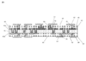
- FIG. 5 is a cross-sectional view showing an example of the wiring board according to the present embodiment.
- FIG. 6 is a cross-sectional view showing another example of the wiring board according to the present embodiment.
- FIG. 7 is a diagram showing a manufacturing process of the wiring board according to the present embodiment.
- FIG. 8 is a diagram showing a manufacturing process of the wiring board according to the present embodiment.
- FIG. 9 is a diagram showing a manufacturing process of the wiring board according to the present embodiment.
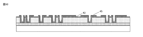
- FIG. 10 is a diagram showing a manufacturing process of a wiring board according to the present embodiment.
- FIG. 11 is a diagram showing a manufacturing process of the wiring board according to the present embodiment.
- FIG. 12 is a diagram showing a manufacturing process of the wiring board according to the present embodiment.
- FIG. 13 is a diagram showing a manufacturing process of the wiring board according to the present embodiment.
- FIG. 14 is a diagram showing a manufacturing process of the wiring board according to the present embodiment.
- FIG. 15 is a diagram showing a manufacturing process of a wiring board according to this embodiment.
- FIG. 16 is a diagram showing a manufacturing process of the wiring board according to the present embodiment.
- FIG. 17 is a diagram showing a manufacturing process of the wiring board according to the present embodiment.
- FIG. 18 is a diagram showing a manufacturing process of the wiring board according to the present embodiment.
- FIG. 19 is a diagram showing a manufacturing process of a wiring board according to an embodiment of the present invention.
- FIG. 20 is a diagram showing a manufacturing process of a wiring board according to an embodiment of the present invention.
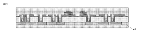
- FIG. 21 is a diagram showing a manufacturing process of a wiring board according to an embodiment of the present invention.
- the term "plane” may refer not only to the surface of the plate-shaped member but also to the interface of the layer substantially parallel to the surface of the plate-shaped member for the layer contained in the plate-shaped member.
- the "upper surface” and “lower surface” mean a plate-shaped member and a surface shown above or below in the drawing when the layer included in the plate-shaped member is illustrated.
- the "side surface” means a plate-shaped member or a portion of a layer included in the plate-shaped member and having a thickness of the surface or layer. Further, a part of the surface and the side surface may be collectively referred to as an "end”.
- "upper” means a vertically upward direction when a plate-shaped member or a layer is placed horizontally.
- the "upper” and the opposite “lower” may be referred to as “Z-axis direction”, and the horizontal direction may be referred to as "X-axis direction” and “Y-axis direction”.
- planar shape” and “planar view” mean a shape when a surface or a layer is visually recognized from above.
- the "cross-sectional shape” and “cross-sectional view” mean the shape when the plate-shaped member or the layer is cut in a specific direction and visually recognized from the horizontal direction.
- central means a central portion that is not a peripheral portion of a surface or layer.
- the “center direction” means a direction from the peripheral portion of the surface or layer toward the center in the planar shape of the surface or layer.
- the “remaining film amount of the wiring layer” refers to the volume obtained by multiplying the pattern area of the wiring layer when the substrate is viewed in a plan view and the film thickness of the wiring layer.
- the "circuit element” is a passive element such as a resistor, a capacitor, an inductor, and a reactor, and preferably means an element that is a component of an LC circuit.
- a circuit element is preferably a component of an LC filter constituting a bandpass filter used for time-division duplex transmission / reception communication in a band of at least 2 GHz or more in a plurality of band communications.
- This LC filter may be configured as a low-pass filter, a high-pass filter, a diplexer equal demultiplexing filter, or a notch filter that removes noise in a specific band.
- the bandpass filter used for time division duplex transmission / reception (TDD: Time Division Duplex) in the band of at least 2 GHz or more among the multiple band communications is configured by an LC filter.
- the reactance element of the LC filter has at least a part of its structure in the wiring board, and by mounting it on an RF component wiring board other than the LC filter, a more compact wiring board can be realized.
- the region located above the built-in circuit element on the surface of the wiring board can be allocated to the mounting of other components, thereby achieving high functionality.
- a compact wiring board can be realized.
- the capacitor has a structure in which a dielectric is sandwiched between two conductor plates.
- the lower electrode 12 is laminated on the insulating resin layer 11 formed directly on the glass substrate (not shown) or on the glass substrate to form a conductor pattern.
- the dielectric layer 13 is laminated on the conductor pattern, and the conductor to be the upper electrode 14 is further laminated on the dielectric layer 13.
- the lower electrode 12 and the upper electrode 14 may have a multilayer structure including a seed layer and a conductive layer.
- FIG. 2 For inductors, the same performance as a spiral coil can be built into a board with through holes.
- a parallel flat plate-shaped glass plate having two rows of through holes is shown in a transparent manner.
- wirings 21 and 22 are formed so as to connect openings of adjacent through holes on the front and back surfaces of the glass plate, and a conductor layer is formed on the inner wall of the through holes 23 communicating with the front and back surfaces of the glass plate. And let it be TGV.
- BPF bandpass filter
- FIG. 4 shows a schematic diagram showing a state in which the capacitor and the inductor shown in the circuit diagram of FIG. 3 are formed inside the wiring board.
- the capacitors C1 to C3 are embedded in the insulating resin layer 43 on the upper surface of the glass core 41, and if it is desired to connect to an electrode outside the wiring board, a via hole is created in the insulating resin layer 43. , Can be connected via the conductor inside it.
- the inductors L1 to L3 can form a solenoid coil by connecting the TGV formed in the through hole 23 in the glass core 41 and the wirings 21 and 22 on the front and back surfaces of the glass core 41. ..
- reference numerals 42 and 48 indicate an adhesion layer.
- the inductors L1 to L3 are embedded inside the glass core 41 and in the insulating resin layer 43 on the front and back surfaces thereof, and the conduction with the electrodes on the outermost layer of the wiring board is the same as that of the capacitors C1 to C3. This can be done through the via hole in the insulating resin layer 43.
- the inductor L2 is a reactance element for an interference suppression adjusting circuit between bandpass filters.
- FIG. 5 is a cross-sectional view showing an example of the wiring board according to the present embodiment.
- the wiring board 30 of the present embodiment is made of glass and includes a first surface 41a, a second surface 41b facing the first surface 41a, and a through hole 44 penetrating from the first surface 41a to the second surface 41b.
- the first adhesion formed so as to be in close contact with the core material (also referred to as a glass core) 41, the first surface 41a and the inner wall of the through hole 44, and further to block the bottom of the through hole 44 on the second surface 41b side.
- the layer 42, the second surface 41b, the second adhesion layer 48 that adheres to the first adhesion layer 42 that closes the bottom of the through hole 44 on the second surface 41b side, and the first adhesion layer 42 are laminated. It has a first wiring layer 45 and a second wiring layer 50 laminated on the second adhesion layer 48.
- An insulating resin layer 43 is laminated on the first wiring layer 45 and the second wiring layer 50, and another wiring layer is formed on the insulating resin layer 43.
- a dielectric layer 51, a seed layer 52, and an upper electrode 54 are formed on the first wiring layer 45 as described later, and a capacitor as shown in FIG. 1 is formed by these. Further, the inductor as shown in FIG. 2 is formed by the first wiring layer 45, the conductor layer in the through via 61 penetrating the insulating resin layer 43, and the wiring pattern 62. Although not particularly described, the capacitor and the inductor may be formed on either the first wiring layer 45 or the second wiring layer 50.
- FIG. 6 is a cross-sectional view showing another example of the wiring board 30 according to the present embodiment.
- the conductive member on one surface of the glass core 41 can be connected to the high frequency component 60 mounted on the wiring board 30 and molded with the mold resin 58 to form a module board.
- the conductive member on the other surface of the glass core 41 can be connected to the mother substrate (not shown).
- Circuit design First, in order to design the circuit, the required capacitance and inductance are calculated by simulation software according to the frequency band of the radio waves that pass or block.
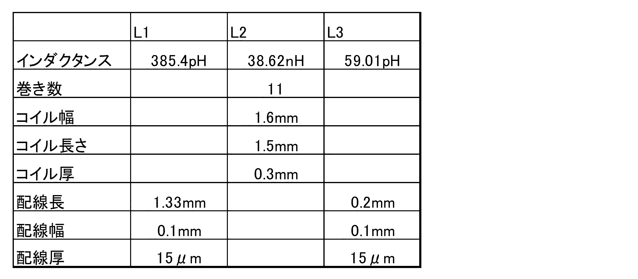
- Tables 1 and 2 show the specifications of the elements for realizing the desired characteristics in the circuit configuration as shown in FIG. 3 for the band of 3400 MHz or more and 3600 MHz or less.
- the inductances of the inductors L1 and L3 are very small, it is not necessary to form a coil, and the self-inductance of one wiring is sufficient. Therefore, the dimensions of the wiring are shown in the table.
- the necessary wiring board is manufactured.
- a low-expansion glass core 41 (thickness 300 ⁇ m, CTE: 3.5 ppm / K) is prepared, and then a through hole 44 having an opening diameter of 80 ⁇ m to 100 ⁇ m is formed in the glass core 41.
- UV laser light is pulsed at the desired position to form the through hole 44, a fragile part is formed in the irradiated glass, and as the second step, hydrofluoric acid is applied to the entire glass plate. Etching with an aqueous solution.
- the fragile portion is selectively etched, and a highly accurate through hole 44 is quickly formed.
- a through hole 44 having a more accurate inner diameter and an inner peripheral surface having no unevenness.
- the support 47 is, for example, a substrate made of a material having a property of transmitting light (transparency).
- the wavelength range of the light transmitted by the support 47 may be, for example, 300 nm or more and 2000 nm or less, or 300 nm or more and 1100 nm or less.
- the support 47 may have a property of transmitting a specific wavelength, such as laser light.
- a glass substrate is preferably used.
- the glass for example, quartz glass, borosilicate glass, non-alkali glass, soda glass, sapphire glass and the like are used.
- the adhesive layer 46 includes a peeling layer and a protective layer, and is a layer for adhering the support 47 and the glass core 41 to each other.
- the release layer is provided on the main surface of the support 47 and contains a resin that can be decomposed by irradiation with light. For example, when the peeling layer is peeled off using laser light, a resin that can be thermally decomposed by being irradiated with laser light having a predetermined wavelength is used as the resin contained in the peeling layer.
- the resin contained in the release layer for example, one of epoxy resin, polyurethane resin, silicone resin, polyester resin, oxetane resin, maleimide resin, or a resin in which two or more of these resins are mixed is used. ..
- the thickness of the adhesive layer 46 is, for example, 20 ⁇ m or more and 100 ⁇ m or less.
- first adhesion layer and the first wiring layer Further, as a part of the first adhesion layer 42 (seed layer) under the wiring layer and on the inner wall of the through hole 44 of the glass core 41, a Ti film and a Cu film are sputtered on the entire surface of the glass core 41 in this order.
- the configuration shown in FIG. 7 is obtained by forming a two-layer film by the method and making the glass surface conductive.
- a close contact layer (a part of the first close contact layer 42) is formed on the film.
- the thickness of the film is set to 50 nm for the Ti film and 300 nm for the Cu film. Ni, Cr, etc. can also be used as the target of sputtering to be used. It is desirable to select this in consideration of adhesion to the substrate, film stress, process resistance, reliability, and the like.
- the first contact layer 42 is used as a seed layer to form the first wiring layer 45 such as the inductor wiring, the lower electrode of the capacitor, and the pad for external connection by the semi-additive method.
- the first wiring layer 45 such as the inductor wiring, the lower electrode of the capacitor, and the pad for external connection by the semi-additive method.
- a trade name RY-3525 (thickness 25 ⁇ m) manufactured by Hitachi Kasei Co., Ltd. is laminated on the upper surface of the glass core 41 as shown in FIG.
- the dry film resist layer 53 is formed.
- the dry film resist layer 53 may be formed by applying a liquid resist. After that, the dry film resist layer 53 is exposed to the dry film resist layer 53 through a mask for forming a conductor pattern, that is, a wiring pattern by a photolithography method, and a wiring pattern (opening) is formed in the resist layer by development.
- the first wiring layer 45 which is a conductive member, is formed with a thickness of 15 ⁇ m.
- copper plating is also deposited on the inner wall of the through hole 44 of the glass core 41 to form a part of the first wiring layer 45.
- the dry film resist is peeled off.
- the surface of the glass core 41 is a portion covered with a first adhesion layer 42 containing Ti / Cu / Ni, and a first wiring in which Cu is further laminated.
- the portion of the layer 45 is mixed.
- the lower electrode of the capacitor is formed at a predetermined position of the conductor pattern.
- a seed layer in this case a layer composed of Ti and Ni, with a material different from Cu, which is the main conductive layer, the stress applied to the glass core 41 can be easily adjusted and the warpage can be easily adjusted. become. Further, by forming the dummy wiring containing Cu at a desired position at the time of forming the dry film resist, it is possible to adjust the warp in more detail.
- a SiN film having a thickness of 200 nm to 400 nm is formed on the entire surface of the glass core 41 on the side where the capacitor is formed by a CVD film forming method to form a dielectric layer 51 of the capacitor. ..
- a Ti film and a Cu film are formed at 50 nm and 300 nm, respectively, by a sputtering film forming method, and the dielectric layer 51 is in this order. A film is formed on the entire top.
- the upper electrode of the capacitor in order to form the upper electrode of the capacitor, only the portion where the upper electrode is formed is exposed from the dry film resist layer 53 by photolithography. Then, as shown in FIG. 14, the upper electrode 54 is formed with a thickness of 9 to 10 ⁇ m by electrolytic copper plating. After that, the dry film resist layer 53 is removed. At this point, a SiN layer or the like is laminated in addition to the capacitor.
- the substrate is treated by a wet etching method to remove the excess portion of the Ti layer and the SiN layer. Therefore, the substrate is treated by a dry etching method.
- the spattered Cu layer at the top of the excess part is removed with an etching solution.
- the sputtered Ti layer underneath and the SiN layer formed by CVD are removed by dry etching. After that, the dry film resist that protected the upper electrode 54 of the capacitor is peeled off and removed.
- FIG. 15 shows the configuration in which the process has been completed so far.
- the glass core 41 is exposed in a portion where there are no wiring, electrodes, dummy patterns, or the like.
- a capacitor (see FIG. 1) composed of a first wiring layer 45, a dielectric layer 51, a seed layer 52, and an upper electrode 54 is formed on the surface of the glass core 41. It is also possible to form part of the continuous wiring that forms the inductor and connect it to the conductor layer TGV.
- an insulating resin (trade name "ABF-GX-T31R") manufactured by Ajinomoto Fine-Techno Co., Ltd. is attached to the upper surface of the glass core 41 to form an insulating resin layer (resin build layer) 43.
- the processing is performed by a vacuum press laminating device, and the insulating resin is sealed inside the through hole 44 of the glass core 41 without voids.
- the thickness of the insulating resin layer 43 is about 35 ⁇ m, and the upper electrode 54 of the capacitor is surely buried.
- the adhesive layer 46 is irradiated with the laser beam L via the support 47 to separate the support 47.
- the laser beam L may be irradiated over the entire support 47, or the laser beam L may be irradiated at a desired position of the support 47.
- the laser beam L is irradiated to the entire support 47 while linearly reciprocating from the viewpoint of reliably decomposing the resin in the adhesive layer 46.
- the laser light L may have a wavelength of, for example, 300 nm or more and 2000 nm or less, preferably 300 nm or more and 1500 nm or less, and more preferably 300 nm or more and 1100 nm or less. May be.
- a device that emits laser light L a YAG laser device that emits light having a wavelength of 1064 nm, a double harmonic YAG laser device that emits light having a wavelength of 532 nm, a semiconductor laser device that emits light having a wavelength of 780 nm or more and 1300 nm or less, and the like. Can be mentioned.
- the support 47 has transparency and transmits the laser beam L. Therefore, the energy of the laser beam L transmitted through the support 47 is absorbed by the adhesive layer 46. The energy of the absorbed laser light L is converted into heat energy in the adhesive layer 46. Due to this thermal energy, the resin of the adhesive layer 46 reaches the thermal decomposition temperature and is thermally decomposed. As a result, the force of the adhesive layer 46 to bond the support 47 and the glass core 41 is weakened.
- a Ti film and a Cu film are formed as a second adhesion layer 48 on the lower surface of the glass core 41 and the bottom of the through hole 44 by a sputtering method in this order. , Makes the lower surface of the glass conductive.
- the thickness of the film is set to 50 nm for the Ti film and 300 nm for the Cu film.
- a second wiring layer 50 such as an inductor wiring, a capacitor lower electrode, and an external connection pad is formed by a semi-additive method using the second adhesion layer 48 as a seed layer.
- a trade name RY-3525 (thickness 25 ⁇ m) manufactured by Hitachi Kasei Co., Ltd. is laminated on the lower surface of the glass core 41 to form a dry film resist layer 53. Form.
- the dry film resist layer 53 may be formed by applying a liquid resist. After that, the dry film resist layer 53 is exposed to the dry film resist layer 53 through a mask for forming a conductor pattern, that is, a wiring pattern by a photolithography method, and a wiring pattern (opening) is formed in the dry film resist layer 53 by development.
- a second wiring layer 50 which is a conductive member, is formed with a thickness of 15 ⁇ m.
- copper plating is also deposited on the bottom of the through hole 44 of the glass core 41 (the portion blocked by the first adhesion layer 42).
- the substrate is treated by a wet etching method in order to remove the excess wiring portion, and the substrate is treated by the dry etching method in order to remove the Ti layer in the excess portion.
- the spattered Cu layer at the top of the excess part is removed with an etching solution.
- the sputtered Ti layer underneath is removed by dry etching.
- the dry film resist layer 53 that protected the second wiring layer 50 is peeled off and removed.
- an insulating resin (trade name "ABF-GX-T31R") manufactured by Ajinomoto Fine-Techno Co., Ltd. is attached to the lower surface of the glass core 41 to form an insulating resin layer (resin build layer). ) 43 is formed.
- the processing is performed by a vacuum press laminating device, and the insulating resin is sealed in the wiring pattern of the second wiring layer 50 without voids.
- the thickness of the insulating resin layer 43 is about 35 ⁇ m, and the wiring pattern of the second wiring layer 50 is surely buried.
- the insulating resin layer 43 is penetrated at a position where conduction is desired, and as shown in FIG. 5, a through hole 56 reaching the wiring layer of the glass core is formed.
- the diameter of the through hole 56 is preferably about 60 ⁇ m.
- the conductive seed layer 57 is formed not only on the front and back surfaces but also on the inner wall of the hole previously formed by laser processing.
- dry film resist DR is attached to both sides of the substrate, and an opening is provided in the portion where wiring is desired by the photolithography method. Then, the substrate is electrolytically plated to form wiring with a thickness of 15 ⁇ m. Further, in this electrolytic plating process, the inside of the through hole 56 in the insulating resin layer 43 is also filled with copper, and the continuity with the second wiring layer 50 on the surface of the glass core 41 is ensured.
- the basic wiring board 30 including the built-in element for the LC circuit as shown in FIG. 5 is completed.
- the build-up wiring on the lower side of the glass core 41 is shown as if it has a copper layer, assuming that it will be ground for the capacitors and inductors built in the wiring board. This is not always the case with an actual wiring board, and it is sufficient that a predetermined capacitor and inductor are grounded when the wiring board is completed.
- a planar (for example, spiral) reactance element can be formed on the surface of the glass core 41 or the insulating resin layer 43. Further, it is possible to arrange an electrically neutral through hole between the reactance elements to reduce the loss due to mutual induction, and it is also possible to provide a capacitance in the through hole.
- C 75 to 85% is often set in consideration of the dummy wiring.
- the influence of the first wiring layer 45 on the warp of the wiring board 30 having a relatively thin glass core is dominated by the residual copper ratio C of the first wiring layer 45. In actual wiring board design, it is the residual copper ratio that has the greatest effect on the warp of the board.
- a dummy pattern or the like is formed so that the difference in the residual copper ratio between the front and back surfaces of the substrate does not occur as much as possible, and the difference in the residual copper ratio between the front and back surfaces is adjusted to be within 10%, for example. If such adjustment is as designed, the warp of the substrate will not be so large, but there may be a case where it is desired to further suppress the warp of the board. In such a case, the present embodiment can be applied to make fine adjustments to the warp.
- the warpage of the wiring board 30 can be suppressed by relatively increasing the rigidity of the first adhesion layer 42.
- the Young's modulus of the first adhesion layer 42 is set too low, it may become brittle and cracks or the like may occur.
- the Young's modulus of the material of the first adhesion layer 42 is set to be 0.1 to 0.85 times the Young's modulus of the material of the first wiring layer 45.
- the film thickness and the film thickness ratio of the first adhesion layer 42 and the first wiring layer 45 it becomes possible to adjust the film stress applied to the glass core 41 in more detail, and the wiring board 30 can be adjusted. It is possible to adjust the warp of.
- the pattern and film thickness of each layer are generally different, which causes warpage.
- the configurations of the first adhesion layer 42 and the first wiring layer 45 are different, it is possible to adjust the total film stress applied to the glass core 41 and adjust the warp. Specifically, it is possible to change the number of films of the first adhesion layer 42, further change the film thickness of each layer of the first adhesion layer 42, and the like.
Landscapes
- Engineering & Computer Science (AREA)
- Microelectronics & Electronic Packaging (AREA)
- Manufacturing & Machinery (AREA)
- Chemical & Material Sciences (AREA)
- Inorganic Chemistry (AREA)
- Production Of Multi-Layered Print Wiring Board (AREA)
Abstract
反りが少なく、小型で、接続信頼性の高い高周波モジュールを得るため、第1面と、前記第1面と対向する第2面と、前記第1面から前記第2面まで貫通する貫通穴とを備えたガラス製のコア材と、前記第1面と前記貫通穴の内壁とに密着し、さらに前記貫通穴の前記第2面側の底部をふさぐようにして形成された第1の密着層と、前記第2面と、前記貫通穴の前記第2面側の底部をふさぐ第1の密着層に密着する第2の密着層と、前記第1の密着層に積層された第1の配線層と、前記第2の密着層に積層された第2の配線層と、を有し、前記第1の配線層の全面積をA、前記第1の配線層において銅が占める面積をBとした場合、前記第1の配線層の残銅率Cは、C=B/A(%)で表され、C=70~100%であり、前記第1の密着層の素材のヤング率が、前記第1の配線層の素材のヤング率の0.1~0.85倍である。
Description
本発明は、配線基板に関する。
スマートフォンなどの高機能携帯端末の急激な普及を可能にしている無線通信システムは、RFフロントエンドモジュール(RFFM:Radio Frequency Front-end Module)の高機能化により支えられている。RFFMは、フィルタ・パワーアンプ(PA:Power amplifier)・ローノイズアンプ(LNA:Low Noise amplifier)・RFスイッチから構成されている。RFFMは、部品の統合化が進むにつれて回路が複雑になり、部品点数も増加する傾向にある。
特に、RFFMの小型、薄型、多機能化等に伴いRFFMに搭載する部品点数が増え、それに対応するためRFFM用パッケージの低背化の要求が高まっている。このようなRFFM用パッケージの低背化を実現するために、薄型多層配線基板を採用することが知られている。
従来、薄型多層配線基板の積層樹脂を薄くする手法によりRFFM全体の低背化を実現することが、広く行なわれていた。
ここで、半導体チップ等の電子部品を実装するための薄型多層配線基板として、様々な形状・構造のものが提案されている。例えば、特許文献1に示すように、内層配線層を中心にしてその内層配線層の上下両側に絶縁層が形成され、それら絶縁層にそれぞれ形成されたビア配線を介して内層配線層が接続される構造を有する薄型多層配線基板が知られている。
薄型多層配線基板において、接続信頼性をどのように確保するかという課題がある。特に、配線基板が薄くなることにより、基板の反りがより顕著になり、実装歩留まりの低下、信頼性の低下などの課題が発生している。
本発明は、かかる課題に鑑みてなされたものであり、例えば高機能携帯端末の低背化に対応でき、薄形でありながら基板の反りを低減し、接続信頼性に優れた配線基板を提供することを目的とする。
上記課題を解決するために、代表的な本発明の配線基板の一つは、
第1面と、前記第1面と対向する第2面と、前記第1面から前記第2面まで貫通する貫通穴とを備えたガラス製のコア材と、
前記第1面と前記貫通穴の内壁とに密着し、さらに前記貫通穴の前記第2面側の底部をふさぐようにして形成された第1の密着層と、
前記第2面と、前記貫通穴の前記第2面側の底部をふさぐ第1の密着層に密着する第2の密着層と、
前記第1の密着層に積層された第1の配線層と、
前記第2の密着層に積層された第2の配線層と、を有し、
前記第1の配線層の全面積をA、前記第1の配線層において銅が占める面積をBとした場合、前記第1の配線層の残銅率Cは、C=B/A(%)で表され、
C=70~100%のときに、前記第1の密着層の素材のヤング率を、前記第1の配線層の素材のヤング率の0.1~0.85倍とすることを特徴とする。
第1面と、前記第1面と対向する第2面と、前記第1面から前記第2面まで貫通する貫通穴とを備えたガラス製のコア材と、
前記第1面と前記貫通穴の内壁とに密着し、さらに前記貫通穴の前記第2面側の底部をふさぐようにして形成された第1の密着層と、
前記第2面と、前記貫通穴の前記第2面側の底部をふさぐ第1の密着層に密着する第2の密着層と、
前記第1の密着層に積層された第1の配線層と、
前記第2の密着層に積層された第2の配線層と、を有し、
前記第1の配線層の全面積をA、前記第1の配線層において銅が占める面積をBとした場合、前記第1の配線層の残銅率Cは、C=B/A(%)で表され、
C=70~100%のときに、前記第1の密着層の素材のヤング率を、前記第1の配線層の素材のヤング率の0.1~0.85倍とすることを特徴とする。
本発明によれば、例えば高機能携帯端末の低背化に対応でき、薄形でありながら基板の反りを低減し、接続信頼性に優れた配線基板を提供することができる。
上記した以外の課題、構成及び効果は、以下の実施形態の説明により明らかにされる。
上記した以外の課題、構成及び効果は、以下の実施形態の説明により明らかにされる。
<実施形態>
以下に、本発明の実施形態について、図面を参照して説明する。また、以下に示す実施形態は、本発明の技術的思想を具体化するための装置や方法を例示するものであって、本発明の技術的思想は、構成部品の材質、形状、構造、配置等を記載されたものに特定するものではない。本発明の技術的思想は、特許請求の範囲に記載された請求項が規定する技術的範囲内において、種々の変更を加えることができる。
以下に、本発明の実施形態について、図面を参照して説明する。また、以下に示す実施形態は、本発明の技術的思想を具体化するための装置や方法を例示するものであって、本発明の技術的思想は、構成部品の材質、形状、構造、配置等を記載されたものに特定するものではない。本発明の技術的思想は、特許請求の範囲に記載された請求項が規定する技術的範囲内において、種々の変更を加えることができる。
なお、本開示において、「面」とは、板状部材の面のみならず、板状部材に含まれる層について、板状部材の面と略平行な層の界面も指すことがある。また、「上面」、「下面」とは、板状部材や板状部材に含まれる層を図示した場合の、図面上の上方又は下方に示される面を意味する。
また、「側面」とは、板状部材や板状部材に含まれる層における面や層の厚みの部分を意味する。さらに、面の一部及び側面を合わせて「端部」ということがある。
また、「上方」とは、板状部材又は層を水平に載置した場合の垂直上方の方向を意味する。さらに、「上方」及びこれと反対の「下方」については、これらを「Z軸方向」ということがあり、水平方向については、「X軸方向」、「Y軸方向」ということがある。
また、「平面形状」、「平面視」とは、上方から面又は層を視認した場合の形状を意味する。さらに、「断面形状」、「断面視」とは、板状部材又は層を特定の方向で切断した場合の水平方向から視認した場合の形状を意味する。
さらに、「中心部」とは、面又は層の周辺部ではない中心部を意味する。そして、「中心方向」とは、面又は層の周辺部から面又は層の平面形状における中心に向かう方向を意味する。
「配線層の残膜量」とは、基板を平面視したときの配線層のパターン面積と、配線層の膜厚とを掛け合わせて得られる体積を言う。
また、「側面」とは、板状部材や板状部材に含まれる層における面や層の厚みの部分を意味する。さらに、面の一部及び側面を合わせて「端部」ということがある。
また、「上方」とは、板状部材又は層を水平に載置した場合の垂直上方の方向を意味する。さらに、「上方」及びこれと反対の「下方」については、これらを「Z軸方向」ということがあり、水平方向については、「X軸方向」、「Y軸方向」ということがある。
また、「平面形状」、「平面視」とは、上方から面又は層を視認した場合の形状を意味する。さらに、「断面形状」、「断面視」とは、板状部材又は層を特定の方向で切断した場合の水平方向から視認した場合の形状を意味する。
さらに、「中心部」とは、面又は層の周辺部ではない中心部を意味する。そして、「中心方向」とは、面又は層の周辺部から面又は層の平面形状における中心に向かう方向を意味する。
「配線層の残膜量」とは、基板を平面視したときの配線層のパターン面積と、配線層の膜厚とを掛け合わせて得られる体積を言う。
また、「回路素子」とは、抵抗器、キャパシタ、インダクタ、リアクトルなどの受動素子であり、好ましくはLC回路の構成要素となる素子をいう。かかる回路素子は、複数帯域通信の内、少なくとも2GHz以上の帯域で時分割二重化送受通信に使用するバンドパスフィルタを構成するLCフィルタの部品であると好ましい。このLCフィルタは、ローパスフィルタ、ハイパスフィルタ、ダイプレクサ等分波フィルタや、特定帯域のノイズを除去する、ノッチフィルタとして構成しても良い。
かかる配線基板において、該複数帯域通信の内、少なくとも2GHz以上の帯域で時分割二重化送受通信(TDD: Time Division Duplex)に使用するバンドパスフィルタをLCフィルタで構成していると好ましい。該LCフィルタのリアクタンス素子は、少なくともその構造の一部を配線基板内に有すると好ましく、また該LCフィルタ以外のRF部品配線基板に実装することで、よりコンパクトな配線基板を実現できる。
本実施形態においては、配線基板に回路素子を内蔵することで、配線基板表面における、内蔵された回路素子の上方に位置する領域を、他の部品の実装に充てることができ、これにより高機能でありながらコンパクトな配線基板を実現できる。
次に、ガラス板をコア材として、その両面に配線層と絶縁樹脂層を片側ずつ形成した基板を例にとって、LC回路を構成する回路素子としてのキャパシタとインダクタの例を、それぞれ説明する。
キャパシタについては、二枚の導体板の間に誘電体を挟んだ構造とする。キャパシタの例としては、図1に示すように、不図示のガラス基板直上に、またはガラス基板上に形成した絶縁樹脂層11の上に、下電極12を積層して導体パターンを形成し、かかる導体パターンの上に誘電体層13を積層し、さらにその上に上電極14となる導体を積層したものである。下電極12と上電極14は、シード層と導電層からなる多層構造であっても良い。
インダクタについては、らせん状のコイルと同様の性能を、貫通穴を備えた基板に内蔵することができる。図2においては、2列に並んだ貫通穴を有する平行平板状のガラス板を透明化して図示している。図2において、ガラス板の表裏面において隣接する貫通穴の開口部同士を接続するように配線21,22を形成し、またガラス板の表裏面を連通する貫通穴23の内壁に導体層を形成し、TGVとする。
次に、基板内部に形成されるLC回路によるバンドパスフィルタ(BPF)について、説明する。BPFの基本的な回路図は、図3のようになる。そして、回路中のキャパシタの電気容量(以下キャパシタンス)とインダクタの誘導係数(以下インダクタンス)を適切に設定することによって、所望の帯域の周波数のみを通過させ、それ以外を遮断するバンドパス効果を発現させることができる。
図3の回路図に示したキャパシタとインダクタを、配線基板内部に形成した状態を示す模式図を、図4に示す。全体としてキャパシタC1~C3は、ガラスコア41の上表面上の絶縁樹脂層43に埋設されるようになっており、配線基板外部の電極と接続したい場合には、絶縁樹脂層43にビアホールを作り、その内部の導体を介して接続できる。
図4に示すように、インダクタL1~L3は、ガラスコア41内の貫通穴23内に形成されたTGVと、ガラスコア41の表裏面の配線21,22をつないでソレノイドコイルを作ることができる。図4において、詳細は後述するが、符号42,48は密着層を示している。インダクタL1~L3本体は、ガラスコア41の内部と、その表裏面の絶縁樹脂層43に埋設されるようになっており、配線基板最外層の電極との導通は、キャパシタC1~C3と同様に、絶縁樹脂層43内のビアホールを介して行うことができる。なお、インダクタL2は、バンドパスフィルタ間の干渉抑制調整回路用のリアクタンス素子である。
<配線基板の例>
図5は、本実施形態にかかる配線基板の一例を示す断面図である。
本実施形態の配線基板30は、第1面41aと、第1面41aと対向する第2面41bと、第1面41aから第2面41bまで貫通する貫通穴44とを備えたガラス製のコア材(ガラスコアともいう)41と、第1面41aと貫通穴44の内壁とに密着し、さらに貫通穴44の第2面41b側の底部をふさぐようにして形成された第1の密着層42と、第2面41bと、貫通穴44の第2面41b側の底部をふさぐ第1の密着層42に密着する第2の密着層48と、第1の密着層42に積層された第1の配線層45と、第2の密着層48に積層された第2の配線層50と、を有する。
図5は、本実施形態にかかる配線基板の一例を示す断面図である。
本実施形態の配線基板30は、第1面41aと、第1面41aと対向する第2面41bと、第1面41aから第2面41bまで貫通する貫通穴44とを備えたガラス製のコア材(ガラスコアともいう)41と、第1面41aと貫通穴44の内壁とに密着し、さらに貫通穴44の第2面41b側の底部をふさぐようにして形成された第1の密着層42と、第2面41bと、貫通穴44の第2面41b側の底部をふさぐ第1の密着層42に密着する第2の密着層48と、第1の密着層42に積層された第1の配線層45と、第2の密着層48に積層された第2の配線層50と、を有する。
第1の配線層45と第2の配線層50には、絶縁樹脂層43が積層され、その上には別の配線層が形成されている。
第1の配線層45上には、後述するようにして誘電体層51,シード層52、上電極54が形成され、これらにより図1に示すようなキャパシタが形成される。また、第1の配線層45と、絶縁樹脂層43を貫通するスルービア61内の導体層と,配線パターン62とで、図2に示すようなインダクタが形成される。特に説明しないが、キャパシタとインダクタは、第1の配線層45と第2の配線層50のいずれに形成してもよい。
図6は、本実施形態にかかる配線基板30の別な例を示す断面図である。図6に示すように、ガラスコア41の一方の面における導電性部材を、配線基板30に実装される高周波部品60に接続し、モールド樹脂58でモールドしてモジュール基板とすることができる。このとき、ガラスコア41の他方の面における導電性部材を、マザー基板(不図示)に接続することができる。
<基板作成プロセス>
次に、図7~21を用いて、ガラス基板を用いた配線基板作成プロセスの一例を示す。
次に、図7~21を用いて、ガラス基板を用いた配線基板作成プロセスの一例を示す。
(回路設計)
まず回路設計を行うため、通過又は遮断する電波の周波数帯域に応じて、必要なキャパシタンスとインダクタンスを、シミュレーションソフトによって算出する。例えば3400MHz以上、3600MHz以下の帯域について、図3に示すような回路構成において、所望の特性を実現するための素子の仕様を表1、表2に示す。ここで、インダクタL1とL3については、インダクタンスが非常に小さいため、コイルの形状にする必要がなく、一本の配線の自己インダクタンスで足りるため、表中では、その配線の寸法について示してある。
まず回路設計を行うため、通過又は遮断する電波の周波数帯域に応じて、必要なキャパシタンスとインダクタンスを、シミュレーションソフトによって算出する。例えば3400MHz以上、3600MHz以下の帯域について、図3に示すような回路構成において、所望の特性を実現するための素子の仕様を表1、表2に示す。ここで、インダクタL1とL3については、インダクタンスが非常に小さいため、コイルの形状にする必要がなく、一本の配線の自己インダクタンスで足りるため、表中では、その配線の寸法について示してある。

2499MHz以上、2690MHz以下の帯域用のBPFについても、同様の手順によって、キャパシタンス、インダクタンスを計算し、必要な回路の設計を行う(数値については省略)。
(ガラスコアと支持体の接合、及びビア内へのシード層の形成)
以上の回路設計に基づいて、必要な配線基板を製作する。まず、低膨張のガラスコア41(厚さ300μm、CTE:3.5ppm/K)を準備し、次いで、かかるガラスコア41に開口径80μm~100μmの貫通穴44を形成する。形成にあたっては、第一段階として、貫通穴44の形成を所望する位置にUVレーザー光をパルス照射し、照射されたガラスに脆弱部を作り、第二段階として、ガラス板全体に対してフッ酸水溶液によるエッチングを行う。
以上の回路設計に基づいて、必要な配線基板を製作する。まず、低膨張のガラスコア41(厚さ300μm、CTE:3.5ppm/K)を準備し、次いで、かかるガラスコア41に開口径80μm~100μmの貫通穴44を形成する。形成にあたっては、第一段階として、貫通穴44の形成を所望する位置にUVレーザー光をパルス照射し、照射されたガラスに脆弱部を作り、第二段階として、ガラス板全体に対してフッ酸水溶液によるエッチングを行う。
これにより脆弱部が選択的にエッチングされ、高精度な貫通穴44が迅速に形成される。ガラスエポキシ基板を用いる場合と比較すると、より高精度な内径を持ち且つ凹凸のない内周面を有する貫通穴44を形成できることとなる。
次に、接着層46付きの支持体47を貼り合わせる。支持体47は、例えば光を透過する性質(透明性)を有する材料から構成される基板である。支持体47が透過する光の波長の範囲は、例えば300nm以上、2000nm以下でもよく、300nm以上、1100nm以下でもよい。支持体47は、例えばレーザー光のような特定の波長を透過する性質を有するものでもよい。
支持体47には、例えばガラス基板が好適に用いられる。ガラスとしては、例えば石英ガラス、ホウケイ酸ガラス、無アルカリガラス、ソーダガラス、又はサファイアガラス等が用いられる。支持体47の主面47aの最大高さ粗さRzを0.01μm以上とすることによって、支持体47のコストを抑制することができる。支持体47の主面47aの最大高さ粗さRzを5μm以下とすることによって、主面47aの凹凸に起因した第1の配線層45の断線及び短絡等を抑制できる。
接着層46は、剥離層及び保護層を含み支持体47とガラスコア41とを互いに接着するための層である。剥離層は、支持体47の主面上に設けられており、光の照射により分解可能な樹脂を含んでいる。例えばレーザー光を用いて剥離層を剥離する場合、剥離層に含まれる樹脂として、所定波長のレーザー光が照射されることによって熱分解可能な樹脂が用いられる。
剥離層に含まれる樹脂としては、例えばエポキシ樹脂、ポリウレタン樹脂、シリコーン樹脂、ポリエステル樹脂、オキセタン樹脂、及びマレイミド樹脂の内の1種又はこれらの樹脂の2種類以上が混合された樹脂等が用いられる。接着層46の厚さは、例えば20μm以上、100μm以下である。
(第1の密着層と第1の配線層の形成)
さらに、配線層の下およびガラスコア41の貫通穴44の内壁の第1の密着層42(シード層)の一部として、ガラスコア41の表面全面にTi膜とCu膜を、この順序でスパッタリング法にて2層製膜して、ガラス表面の導電化を行うことにより、図7の構成を得る。
さらに、配線層の下およびガラスコア41の貫通穴44の内壁の第1の密着層42(シード層)の一部として、ガラスコア41の表面全面にTi膜とCu膜を、この順序でスパッタリング法にて2層製膜して、ガラス表面の導電化を行うことにより、図7の構成を得る。
支持体47により貫通穴44の下面側開口が遮蔽されているため、スパッタリングによって、ガラスコア41の第1面41aおよび貫通穴44の内壁と、さらに貫通穴44の下面側開口をふさぐ支持体47に、密着層(第1の密着層42の一部)が成膜される。その膜の厚さは、Ti膜を50nm、Cu膜を300nmに設定する。使用するスパッタリングのターゲットとしては、Ni、Crなども用いる事が可能である。これは、基板への密着性、膜応力、プロセス耐性、信頼性等を考慮して選定することが望ましい。
ついで、貫通穴44内壁のスパッタ膜の薄い部分を補完するためおよび、基板の反りを調整するために、無電解ニッケルめっきを施し、Ti/Cu/Niからなる密着層(第1の密着層42の残り)とする。加工はガラスコア41の表裏全面と貫通穴44内に対して行い、めっき厚さは0.2μmに設定した。以上により第1の密着層42が形成される。
図8に示すように、第1の密着層42をシード層として、セミアディティブ法によって、インダクタの配線、キャパシタの下電極、外部接続用のパッドなどの第1の配線層45を形成する。第1の配線層45に導体パターンを形成するために、図9に示すように、ガラスコア41の上面に、例えば日立化成株式会社製、商品名RY-3525(厚さ25μm)をラミネートしてドライフィルムレジスト層53を形成する。
ドライフィルムレジスト層53の形成は、液状レジスト塗布でもよい。その後、フォトリソグラフィー法により、導体パターンすなわち配線パターンを形成するためのマスクを介してドライフィルムレジスト層53に露光し、現像によってレジスト層に配線パターン(開口部)を形成する。
次に、電解銅めっきによって上記開口部に銅を析出させ、導電性部材である第1の配線層45を15μmの厚さで形成する。この段階において、ガラスコア41の貫通穴44内壁にも銅めっきが析出して、第1の配線層45の一部を構成する。
続いて、ドライフィルムレジストを剥離する。この段階において、図10に示すように、ガラスコア41の表面はTi/Cu/Niを含む第1の密着層42で覆われた部分と、さらにその上にCuが積層された第1の配線層45の部分が混在している。図10の工程で、導体パターンの所定の位置には、キャパシタの下電極が形成される。
このように、主導電層であるCuと異なる材料でシード層、この場合はTiとNiからなる層を形成することで、ガラスコア41に掛かる応力が調整しやすくなり反りを調整することが容易になる。また、前記ドライフィルムレジストの形成時に、Cuを含むダミー配線を所望の位置に形成しておくことで、より詳細に反りを調整することが可能となる。
図11に示すように、まずガラスコア41のキャパシタを形成する側の面全体に、CVD製膜法にて、厚さ200nm乃至400nmでSiN膜を形成してキャパシタの誘電体層51を形成する。
更に、図12に示すように、キャパシタの上電極を形成する際のシード層52として、スパッタ製膜法にて、Ti膜とCu膜をおのおの50nm、300nmにて、この順序で誘電体層51の上全体に製膜する。
続いて、図13に示すように、キャパシタの上電極を形成すべく、フォトリソグラフィーにて、上電極を形成する部分のみをドライフィルムレジスト層53から露出させた状態とする。ついで図14に示すように、電解銅めっきにて、厚さ9~10μmにて上電極54を形成する。その後、ドライフィルムレジスト層53を除去する。この時点では、キャパシタ以外にもSiN層などが積層されている。
そこで、余分な密着層、めっきシード層などを除去すべく、まずフォトリソグラフィーにて、上記キャパシタの上電極54上のみをドライフィルムレジスト(不図示)で保護する。
続いて、キャパシタの上電極54を製膜する際のスパッタ銅層のうち、余分な部分を除去するべく、ウエットエッチング法にて基板を処理し、余分な部分のTi層、SiN層を除去すべく、基板をドライエッチング法にて処理する。
より具体的には、まず余分な部分で一番上にあるスパッタCu層をエッチング液にて除去する。つぎに、その下のスパッタTi層とCVD製膜したSiN層を、ドライエッチングにて除去する。そのあとで、キャパシタの上電極54を保護していたドライフィルムレジストを剥離除去する。
つぎに、キャパシタの下電極およびその他の、ガラスコア41の表面に形成されている導電層のシード層を除去すべく、Ni,Tiの順に、ウエットエッチング工法にて処理する。これにより、その下方にあるスパッタCu層も同時に除去される。一方、配線、キャパシタ電極などを形成しているCu層は、多少はエッチング液に溶けるが、その厚さが比較的大きいため、完全に除去されてしまうことはない。そのあとで、スパッタTi層をエッチングにて除去する。
ここまで工程を終えた構成を図15に示す。この段階で、配線、電極、ダミーパターンなどのない部分には、ガラスコア41が露出することとなる。以上の結果として、ガラスコア41の表面には、第1の配線層45、誘電体層51,シード層52,上電極54からなるキャパシタ(図1参照)が形成される。またインダクタを形成する連続する配線の一部を形成して、導体層TGVとつなぐこともできる。
つぎに、ガラスコア41の上面に、例えば味の素ファインテクノ株式会社製の絶縁樹脂(商品名「ABF-GX-T31R」)を貼付して、絶縁樹脂層(樹脂ビルド層)43を形成する。加工は真空プレスラミネート装置にて、ガラスコア41の貫通穴44の内部にボイドなく絶縁樹脂を封入する。絶縁樹脂層43の厚さは35μm程度とし、キャパシタの上電極54まで確実に埋没するようにする。
(支持体の分離)
次に、図16に示すように、支持体47を介して接着層46にレーザー光Lを照射して、支持体47を分離する。支持体47全体に渡ってレーザー光Lを照射してもよいし、支持体47の所望の位置にレーザー光Lを照射してもよい。配線基板の製造では、接着層46内の樹脂を確実に分解する観点から、直線的に往復させながら支持体47全体にレーザー光Lを照射する。
次に、図16に示すように、支持体47を介して接着層46にレーザー光Lを照射して、支持体47を分離する。支持体47全体に渡ってレーザー光Lを照射してもよいし、支持体47の所望の位置にレーザー光Lを照射してもよい。配線基板の製造では、接着層46内の樹脂を確実に分解する観点から、直線的に往復させながら支持体47全体にレーザー光Lを照射する。
レーザー光Lは、例えば300nm以上、2000nm以下の波長を有してもよく、好ましくは300nm以上、1500nm以下の波長を有していてもよく、より好ましくは300nm以上、1100nm以下の波長を有していてもよい。レーザー光Lを出射する装置の一例として1064nmの波長の光を出射するYAGレーザー装置、532nmの波長の2倍高調波YAGレーザー装置、又は780nm以上1300nm以下の波長の光を出射する半導体レーザー装置等が挙げられる。
支持体47は透明性を有しており、レーザー光Lを透過する。よって、支持体47を透過したレーザー光Lのエネルギーは、接着層46に吸収される。吸収されたレーザー光Lのエネルギーは、接着層46内にて熱エネルギーに変換される。この熱エネルギーによって、接着層46の樹脂は熱分解温度に達し、熱分解する。これによって、接着層46が支持体47とガラスコア41とを接着する力が弱まる。
(第2の密着層と第2の配線層の形成)
次に、図17に示すように、ガラスコア41の下面および貫通穴44の底部に第2の密着層48として、Ti膜とCu膜を、この順序でスパッタリング法にて2層製膜して、ガラス下面の導電化を行う。膜の厚さは、Ti膜を50nm、Cu膜を300nmに設定する。
次に、図17に示すように、ガラスコア41の下面および貫通穴44の底部に第2の密着層48として、Ti膜とCu膜を、この順序でスパッタリング法にて2層製膜して、ガラス下面の導電化を行う。膜の厚さは、Ti膜を50nm、Cu膜を300nmに設定する。
図18に図示するように、第2の密着層48をシード層として、セミアディティブ法によって、インダクタの配線、キャパシタの下電極、外部接続用のパッドなどの第2の配線層50を形成する。さらに第2の配線層50に導体パターンを形成するために、ガラスコア41の下面に、例えば日立化成株式会社製の商品名RY-3525(厚さ25μm)をラミネートしてドライフィルムレジスト層53を形成する。
ドライフィルムレジスト層53の形成は、液状レジスト塗布でもよい。その後、フォトリソグラフィー法により、導体パターンすなわち配線パターンを形成するためのマスクを介してドライフィルムレジスト層53に露光し、現像によってドライフィルムレジスト層53に配線パターン(開口部)を形成する。
次に、図19に示すように、電解銅めっきによって上記開口部に銅を析出させ、導電性部材である第2の配線層50を15μmの厚さで形成する。この段階において、ガラスコア41の貫通穴44の底部(第1の密着層42でふさがれた部位)にも銅めっきが析出する。
続いて、図20に示すように、余分な配線部分を除去するべく、ウエットエッチング法にて基板を処理し、余分な部分のTi層を除去すべく、基板をドライエッチング法にて処理する。
より具体的には、まず余分な部分で一番上にあるスパッタCu層をエッチング液にて除去する。つぎに、その下のスパッタTi層を、ドライエッチングにて除去する。そのあとで、第2の配線層50を保護していたドライフィルムレジスト層53を剥離除去する。
つぎに、図21に示すように、ガラスコア41の下面に、例えば味の素ファインテクノ株式会社製の絶縁樹脂(商品名「ABF-GX-T31R」)を貼付して、絶縁樹脂層(樹脂ビルド層)43を形成する。加工は真空プレスラミネート装置にて、第2の配線層50の配線パターンにボイドなく絶縁樹脂を封入する。絶縁樹脂層43の厚さは35μm程度とし、第2の配線層50の配線パターンまで確実に埋没するようにする。
さらにレーザー加工によって、導通をとりたい位置に絶縁樹脂層43を貫通させ、図5に示すように、ガラスコアの配線層に達するスルーホール56を形成する。スルーホール56の直径は60μm程度が好ましい。
図示していないが、ガラスコア41の表裏面の絶縁樹脂層43を、アルカリ系の表面粗化液にて処理し、算術表面粗さRa=60nmになるように調整する。これは、次の工程にて、シード層の密着力を高めるためのものである。
つぎに、ガラスコア41の表裏面の絶縁樹脂層43に無電解銅めっきを施し、導電シード層57を形成する。その厚さは0.6μmとすると好ましい。この処理によって、表裏面のみならず、先にレーザー加工にて形成した孔の内壁にも導電シード層57が形成される。
図示していないが、基板両面にドライフィルムレジストDRを貼付し、フォトリソグラフィー法によって、配線を設けたい部分に開口部を設ける。ついで、基板に電解めっきを施し、厚さ15μmにて配線を形成する。また、この電解めっき処理において、絶縁樹脂層43内のスルーホール56の内部も銅で満たされ、ガラスコア41表面の第2の配線層50との導通も確保される。
その後、不要な導電シード層をエッチングで除去する。以上をもって、図5に示すような、LC回路用の内蔵素子を含む基本的な配線基板30が完成する。なお、図中、ガラスコア41の下側のビルドアップ配線については、配線基板に内蔵されるキャパシタ、インダクタにとって、グランドとなる場合を想定して、あたかも銅層があるように示しているが、実際の配線基板では必ずしもそうである必要はなく、配線基板完成時に所定のキャパシタ、インダクタが接地されていればよい。
このあと、必要に応じて、上記の工程を繰り返して、絶縁層、導体配線層を積層し、電子部品を実装してよい。また、ガラスコア41又は絶縁樹脂層43の表面に平面状(たとえば渦巻き状)のリアクタンス素子(コイル)を形成することもできる。また、電気的に中性なスルーホールをリアクタンス素子間に配置し、相互誘導による損失を低減することも可能であり、スルーホール内にキャパシタンスを設けることも可能である。
ここで、第1の配線層45の全面積をA、第1の配線層45において銅が占める面積をBとした場合、第1の配線層45の残銅率Cは、C=B/A(%)で表され、ここではC=70~100%である。なお、第1の配線層45にダミー配線がある場合には、ダミー配線を考慮して、C=75~85%とすることが多い。比較的薄いガラスコアを有する配線基板30の反りに与える第1の配線層45の影響は、第1の配線層45の残銅率Cが支配的となって生じる。
実際の配線基板設計において、基板の反りに最も影響を与えるのは残銅率である。そのため、基板の表裏での残銅率に極力差が生じないように、ダミーパターン等を形成して、例えば表裏の残銅率差が10%以内になるように調整する。かかる調整が設計通りであれば、基板の反りはそれほど大きくはならないが、より基板の反りを抑えたい場合もある。
かかる場合には、本実施形態を適用して反りの微調整を行うことができる。
実際の配線基板設計において、基板の反りに最も影響を与えるのは残銅率である。そのため、基板の表裏での残銅率に極力差が生じないように、ダミーパターン等を形成して、例えば表裏の残銅率差が10%以内になるように調整する。かかる調整が設計通りであれば、基板の反りはそれほど大きくはならないが、より基板の反りを抑えたい場合もある。
かかる場合には、本実施形態を適用して反りの微調整を行うことができる。
一例として、第1の密着層42の素材のヤング率(Ti=106GPa、Ni=199.5GPa)を、第1の配線層45の素材のヤング率(Cu=129.8GPa)よりも低くすることにより、第1の密着層42の剛性を相対的に高めることで、配線基板30の反りを抑えることができる。しかしながら、第1の密着層42のヤング率を低くしすぎると、脆性化することでクラックなどが発生するおそれがある。
そこで本実施形態では、第1の密着層42の素材のヤング率を、第1の配線層45の素材のヤング率の0.1~0.85倍となるように設定することとした。このように、最適なヤング率を設定することで、配線基板30の反りの抑制が有効となる。第2の配線基板50においても、同様な調整を行うと好ましい。
また、第1の密着層42と第1の配線層45の膜厚及び、膜厚比率を調整することで、より詳細にガラスコア41に掛かる膜応力を調整することが可能となり、配線基板30の反りを調整することが可能となる。
特に、ガラスコア41の表裏に所望の配線パターンが形成されたとき、一般的には、各層のパターンや膜厚が異なるため、反りの要因となってしまう。本実施形態によれば、第1の密着層42と第1の配線層45の構成が異なることにより、ガラスコア41に掛かるトータルの膜応力を調整し、反りを調整することが可能となる。具体的には第1の密着層42の膜数を変更したり、さらに第1の密着層42の各層の膜厚を変更するなどが可能である。
11:絶縁樹脂層、12:キャパシタの下電極、13:キャパシタの誘電体層、14:キャパシタの上電極、21・22:配線、23:貫通穴、30:配線基板、41:ガラスコア、42:第1の密着層、43:絶縁樹脂層、44:貫通穴、45:第1の配線層、46:接着層、47:支持体、48:第2の密着層、50:第2の配線層、51:誘電体層、52:シード層、53:ドライフィルムレジスト層、54:キャパシタの上電極、56:貫通穴、57:導電シールド層、58:モールド樹脂、60:高周波部品
Claims (4)
- 第1面と、前記第1面と対向する第2面と、前記第1面から前記第2面まで貫通する貫通穴とを備えたガラス製のコア材と、
前記第1面と前記貫通穴の内壁とに密着し、さらに前記貫通穴の前記第2面側の底部をふさぐようにして形成された第1の密着層と、
前記第2面と、前記貫通穴の前記第2面側の底部をふさぐ第1の密着層に密着する第2の密着層と、
前記第1の密着層に積層された第1の配線層と、
前記第2の密着層に積層された第2の配線層と、を有し、
前記第1の配線層の全面積をA、前記第1の配線層において銅が占める面積をBとした場合、前記第1の配線層の残銅率Cは、C=B/A(%)で表され、
C=70~100%のときに、前記第1の密着層の素材のヤング率を、前記第1の配線層の素材のヤング率の0.1~0.85倍とすることを特徴とする配線基板。 - 前記第1の密着層は、Ni、Ti、Crの少なくとも1つを含み、前記第1の配線層は、Cuを含むことを特徴とする請求項1に記載の配線基板。
- 前記第1の密着層の一部及び前記第1の配線層が無電解めっきにより形成されたことを特徴とする請求項1または2に記載の配線基板。
- 前記第1の配線層は、ダミー配線を有することを特徴とする請求項1~3のいずれか一項に記載の配線基板。
Priority Applications (3)
| Application Number | Priority Date | Filing Date | Title |
|---|---|---|---|
| EP21872314.6A EP4221471A4 (en) | 2020-09-28 | 2021-09-16 | Wiring board |
| CN202180065590.4A CN116210352B (zh) | 2020-09-28 | 2021-09-16 | 布线基板 |
| US18/127,295 US12575029B2 (en) | 2020-09-28 | 2023-03-28 | Wiring board |
Applications Claiming Priority (2)
| Application Number | Priority Date | Filing Date | Title |
|---|---|---|---|
| JP2020161639A JP2022054538A (ja) | 2020-09-28 | 2020-09-28 | 配線基板 |
| JP2020-161639 | 2020-09-28 |
Related Child Applications (1)
| Application Number | Title | Priority Date | Filing Date |
|---|---|---|---|
| US18/127,295 Continuation US12575029B2 (en) | 2020-09-28 | 2023-03-28 | Wiring board |
Publications (1)
| Publication Number | Publication Date |
|---|---|
| WO2022065184A1 true WO2022065184A1 (ja) | 2022-03-31 |
Family
ID=80846645
Family Applications (1)
| Application Number | Title | Priority Date | Filing Date |
|---|---|---|---|
| PCT/JP2021/034064 Ceased WO2022065184A1 (ja) | 2020-09-28 | 2021-09-16 | 配線基板 |
Country Status (5)
| Country | Link |
|---|---|
| US (1) | US12575029B2 (ja) |
| EP (1) | EP4221471A4 (ja) |
| JP (1) | JP2022054538A (ja) |
| CN (1) | CN116210352B (ja) |
| WO (1) | WO2022065184A1 (ja) |
Families Citing this family (2)
| Publication number | Priority date | Publication date | Assignee | Title |
|---|---|---|---|---|
| US12424518B2 (en) * | 2022-02-28 | 2025-09-23 | Qualcomm Incorporated | Capacitor embedded 3D resonator for broadband filter |
| CN117836943A (zh) * | 2022-07-27 | 2024-04-05 | 京东方科技集团股份有限公司 | 功能基板及其制备方法、电子设备 |
Citations (3)
| Publication number | Priority date | Publication date | Assignee | Title |
|---|---|---|---|---|
| JP2004200265A (ja) * | 2002-12-17 | 2004-07-15 | Nikon Corp | プリント配線板 |
| JP2010087402A (ja) * | 2008-10-02 | 2010-04-15 | Hitachi Chem Co Ltd | プリント配線板用多層基板の製造方法 |
| JP2017005205A (ja) * | 2015-06-15 | 2017-01-05 | シャープ株式会社 | 配線基板および配線基板の製造方法 |
Family Cites Families (14)
| Publication number | Priority date | Publication date | Assignee | Title |
|---|---|---|---|---|
| US5126016A (en) * | 1991-02-01 | 1992-06-30 | International Business Machines Corporation | Circuitization of polymeric circuit boards with galvanic removal of chromium adhesion layers |
| JP2000036660A (ja) * | 1998-07-17 | 2000-02-02 | Hitachi Chem Co Ltd | ビルドアップ多層配線板の製造方法 |
| JP4626919B2 (ja) * | 2001-03-27 | 2011-02-09 | ルネサスエレクトロニクス株式会社 | 半導体装置 |
| JP5168838B2 (ja) * | 2006-07-28 | 2013-03-27 | 大日本印刷株式会社 | 多層プリント配線板及びその製造方法 |
| KR101037450B1 (ko) * | 2009-09-23 | 2011-05-26 | 삼성전기주식회사 | 패키지 기판 |
| JP5355380B2 (ja) | 2009-12-25 | 2013-11-27 | 新光電気工業株式会社 | 多層配線基板 |
| JP6467814B2 (ja) * | 2014-08-19 | 2019-02-13 | 凸版印刷株式会社 | 配線基板の製造方法、並びに半導体装置の製造方法 |
| KR102281459B1 (ko) * | 2014-11-05 | 2021-07-27 | 삼성전기주식회사 | 인쇄회로기판 및 그 제조방법 |
| JP6816964B2 (ja) * | 2016-03-10 | 2021-01-20 | 新光電気工業株式会社 | 配線基板、半導体装置及び配線基板の製造方法 |
| JP2019106429A (ja) * | 2017-12-11 | 2019-06-27 | 凸版印刷株式会社 | ガラス配線基板、その製造方法及び半導体装置 |
| JP2019175968A (ja) * | 2018-03-28 | 2019-10-10 | 富士通株式会社 | 回路基板及び回路基板の製造方法 |
| WO2020116228A1 (ja) * | 2018-12-04 | 2020-06-11 | 凸版印刷株式会社 | 回路基板 |
| JP7457657B2 (ja) | 2018-12-27 | 2024-03-28 | デンカ株式会社 | 発光基板及び照明装置 |
| JP7188101B2 (ja) * | 2019-01-15 | 2022-12-13 | 凸版印刷株式会社 | 高周波モジュール用電子基板 |
-
2020
- 2020-09-28 JP JP2020161639A patent/JP2022054538A/ja active Pending
-
2021
- 2021-09-16 WO PCT/JP2021/034064 patent/WO2022065184A1/ja not_active Ceased
- 2021-09-16 EP EP21872314.6A patent/EP4221471A4/en active Pending
- 2021-09-16 CN CN202180065590.4A patent/CN116210352B/zh active Active
-
2023
- 2023-03-28 US US18/127,295 patent/US12575029B2/en active Active
Patent Citations (3)
| Publication number | Priority date | Publication date | Assignee | Title |
|---|---|---|---|---|
| JP2004200265A (ja) * | 2002-12-17 | 2004-07-15 | Nikon Corp | プリント配線板 |
| JP2010087402A (ja) * | 2008-10-02 | 2010-04-15 | Hitachi Chem Co Ltd | プリント配線板用多層基板の製造方法 |
| JP2017005205A (ja) * | 2015-06-15 | 2017-01-05 | シャープ株式会社 | 配線基板および配線基板の製造方法 |
Non-Patent Citations (1)
| Title |
|---|
| See also references of EP4221471A4 * |
Also Published As
| Publication number | Publication date |
|---|---|
| JP2022054538A (ja) | 2022-04-07 |
| CN116210352B (zh) | 2026-04-10 |
| US12575029B2 (en) | 2026-03-10 |
| EP4221471A4 (en) | 2024-03-20 |
| CN116210352A (zh) | 2023-06-02 |
| US20230240009A1 (en) | 2023-07-27 |
| EP4221471A1 (en) | 2023-08-02 |
Similar Documents
| Publication | Publication Date | Title |
|---|---|---|
| KR101076061B1 (ko) | 3차원의 모든 유기체 배선 구조들을 제조하기 위한 방법 | |
| JP7608727B2 (ja) | 高周波フィルタ内蔵ガラスコア配線基板の製造方法 | |
| US11303261B2 (en) | Circuit board | |
| US12200859B2 (en) | Circuit board | |
| KR101740816B1 (ko) | 칩 인덕터 | |
| US12177978B2 (en) | Circuit board | |
| CN104332413A (zh) | 一体化集成t/r组件芯片的3d组装方法 | |
| TWI785868B (zh) | 線路基板及其製造方法 | |
| US12575029B2 (en) | Wiring board | |
| KR102825268B1 (ko) | 웨이브 가이드 패키지와 그 제조방법, 및 패키지 하우징 | |
| WO2005101934A1 (ja) | 複合型電子部品及びその製造方法 | |
| JP7383215B2 (ja) | 回路基板 | |
| JP2021114582A (ja) | 電子部品搭載用回路基板 | |
| JP2005310841A (ja) | 回路モジュール体及びその製造方法 | |
| JP2024134681A (ja) | 配線基板および配線基板の製造方法 |
Legal Events
| Date | Code | Title | Description |
|---|---|---|---|
| 121 | Ep: the epo has been informed by wipo that ep was designated in this application |
Ref document number: 21872314 Country of ref document: EP Kind code of ref document: A1 |
|
| WWE | Wipo information: entry into national phase |
Ref document number: 2021872314 Country of ref document: EP |
|
| NENP | Non-entry into the national phase |
Ref country code: DE |
|
| ENP | Entry into the national phase |
Ref document number: 2021872314 Country of ref document: EP Effective date: 20230428 |