WO2023027104A1 - Dispositif de commande de front d'onde et dispositif optique adaptatif - Google Patents
Dispositif de commande de front d'onde et dispositif optique adaptatif Download PDFInfo
- Publication number
- WO2023027104A1 WO2023027104A1 PCT/JP2022/031870 JP2022031870W WO2023027104A1 WO 2023027104 A1 WO2023027104 A1 WO 2023027104A1 JP 2022031870 W JP2022031870 W JP 2022031870W WO 2023027104 A1 WO2023027104 A1 WO 2023027104A1
- Authority
- WO
- WIPO (PCT)
- Prior art keywords
- optical
- wavefront
- frequency comb
- optical frequency
- control device
- Prior art date
- Legal status (The legal status is an assumption and is not a legal conclusion. Google has not performed a legal analysis and makes no representation as to the accuracy of the status listed.)
- Ceased
Links
Images





Classifications
-
- G—PHYSICS
- G02—OPTICS
- G02F—OPTICAL DEVICES OR ARRANGEMENTS FOR THE CONTROL OF LIGHT BY MODIFICATION OF THE OPTICAL PROPERTIES OF THE MEDIA OF THE ELEMENTS INVOLVED THEREIN; NON-LINEAR OPTICS; FREQUENCY-CHANGING OF LIGHT; OPTICAL LOGIC ELEMENTS; OPTICAL ANALOGUE/DIGITAL CONVERTERS
- G02F1/00—Devices or arrangements for the control of the intensity, colour, phase, polarisation or direction of light arriving from an independent light source, e.g. switching, gating or modulating; Non-linear optics
- G02F1/01—Devices or arrangements for the control of the intensity, colour, phase, polarisation or direction of light arriving from an independent light source, e.g. switching, gating or modulating; Non-linear optics for the control of the intensity, phase, polarisation or colour
-
- G—PHYSICS
- G02—OPTICS
- G02F—OPTICAL DEVICES OR ARRANGEMENTS FOR THE CONTROL OF LIGHT BY MODIFICATION OF THE OPTICAL PROPERTIES OF THE MEDIA OF THE ELEMENTS INVOLVED THEREIN; NON-LINEAR OPTICS; FREQUENCY-CHANGING OF LIGHT; OPTICAL LOGIC ELEMENTS; OPTICAL ANALOGUE/DIGITAL CONVERTERS
- G02F1/00—Devices or arrangements for the control of the intensity, colour, phase, polarisation or direction of light arriving from an independent light source, e.g. switching, gating or modulating; Non-linear optics
- G02F1/29—Devices or arrangements for the control of the intensity, colour, phase, polarisation or direction of light arriving from an independent light source, e.g. switching, gating or modulating; Non-linear optics for the control of the position or the direction of light beams, i.e. deflection
- G02F1/295—Analog deflection from or in an optical waveguide structure]
- G02F1/2955—Analog deflection from or in an optical waveguide structure] by controlled diffraction or phased-array beam steering
-
- G—PHYSICS
- G02—OPTICS
- G02B—OPTICAL ELEMENTS, SYSTEMS OR APPARATUS
- G02B26/00—Optical devices or arrangements for the control of light using movable or deformable optical elements
- G02B26/06—Optical devices or arrangements for the control of light using movable or deformable optical elements for controlling the phase of light
-
- G—PHYSICS
- G02—OPTICS
- G02F—OPTICAL DEVICES OR ARRANGEMENTS FOR THE CONTROL OF LIGHT BY MODIFICATION OF THE OPTICAL PROPERTIES OF THE MEDIA OF THE ELEMENTS INVOLVED THEREIN; NON-LINEAR OPTICS; FREQUENCY-CHANGING OF LIGHT; OPTICAL LOGIC ELEMENTS; OPTICAL ANALOGUE/DIGITAL CONVERTERS
- G02F2203/00—Function characteristic
- G02F2203/15—Function characteristic involving resonance effects, e.g. resonantly enhanced interaction
-
- G—PHYSICS
- G02—OPTICS
- G02F—OPTICAL DEVICES OR ARRANGEMENTS FOR THE CONTROL OF LIGHT BY MODIFICATION OF THE OPTICAL PROPERTIES OF THE MEDIA OF THE ELEMENTS INVOLVED THEREIN; NON-LINEAR OPTICS; FREQUENCY-CHANGING OF LIGHT; OPTICAL LOGIC ELEMENTS; OPTICAL ANALOGUE/DIGITAL CONVERTERS
- G02F2203/00—Function characteristic
- G02F2203/18—Function characteristic adaptive optics, e.g. wavefront correction
-
- G—PHYSICS
- G02—OPTICS
- G02F—OPTICAL DEVICES OR ARRANGEMENTS FOR THE CONTROL OF LIGHT BY MODIFICATION OF THE OPTICAL PROPERTIES OF THE MEDIA OF THE ELEMENTS INVOLVED THEREIN; NON-LINEAR OPTICS; FREQUENCY-CHANGING OF LIGHT; OPTICAL LOGIC ELEMENTS; OPTICAL ANALOGUE/DIGITAL CONVERTERS
- G02F2203/00—Function characteristic
- G02F2203/56—Frequency comb synthesizer
Definitions
- the present invention relates to wavefront control devices and adaptive optics devices. This application claims priority based on Japanese Patent Application No. 2021-137394 filed in Japan on August 25, 2021, the content of which is incorporated herein.
- the captured image is corrected and restored by adaptive optics.
- a direct image obtained from an object to be measured becomes a distorted image under the influence of environmental and spatial fluctuations.
- wavefront control By correcting this distorted image by wavefront control, a clear image formed with high contrast on the imaging surface of a light receiver such as an imaging camera can be obtained.
- wavefront measurement for measuring the shape and state of the acquired wavefront and wavefront control for controlling the wavefront based on information on the measured wavefront are performed.
- Wavefront measurement techniques include, for example, a method using a Shack-Hartmann wavefront sensor equipped with a lens array, and a variable mirror capable of adjusting the orientation of the reflecting surface that intersects the optical axis of incident light. or directly modulating the phase of the incident wavefront by means of a spatial light modulator (SLM).
- SLM spatial light modulator
- a phased array is an approach to speed up wavefront measurement and wavefront control.
- a phased array antenna is realized by a plurality of antennas arranged in an array and phase-controlled electromagnetic waves, and is used in weather radars and ultrasonic diagnostic equipment that use radio waves as electromagnetic waves.
- electromagnetic waves having individually controlled phases are emitted from a plurality of antennas, so wavefront measurement and wavefront control can be performed at the same time.
- optical phased arrays that use light as electromagnetic waves are expected to be applied to LiDAR (light detection and ranging), projectors, and biological fluorescence measurement.
- Patent Document 1 and Non-Patent Documents 1 and 2 disclose a waveguide type optical integrated circuit device as an example of an optical phased array.
- each of a plurality of branch waveguides branched from an input waveguide formed in a planar lightwave circuit or the like in the same number as the antennas is provided with a phase adjustment section.
- the lightwave phase-controlled by the phase adjuster is emitted from the emission end (antenna) of each of the plurality of branch waveguides.
- Conventional optical phased arrays are composed of waveguide-type optical integrated circuit devices, as exemplified in Patent Document 1 and Non-Patent Documents 1 and 2 above.
- waveguide-type optical integrated circuit devices it is necessary to individually control the same number of phase adjustment units as there are branch waveguides, that is, the same number of phase adjustment units as the number of antennas in the optical phased array.
- the space occupied by a plurality of phase adjustment units and phase control devices connected to each of them increases. It is necessary to independently control and calibrate parameters about twice as many as the number of antennas. As the number of antennas increases, control of a plurality of antennas and calibration of parameters for each antenna become complicated.
- substantially monochromatic light has to be used.
- the conventional waveguide type optical phased array in order to broaden the band of the light wave to be subjected to wavefront measurement and wavefront control by the conventional waveguide type optical phased array and to control it at high speed, it is necessary to increase the size of the integrated circuit and the control device, and to increase the control parameters. Growth is inevitable. For this reason, the practicality of the conventional waveguide-type optical phased array was low.
- the present invention provides a wavefront control device and an adaptive optics device capable of performing high-speed wavefront control with simple control regardless of an increase in the number of antennas, and realizing widening the bandwidth of light waves to be controlled.
- the wavefront control device includes an optical frequency comb generator that emits an optical frequency comb having a plurality of optical pulses arranged in numerical order on a time axis, and the optical frequency comb that is incident from the optical frequency comb generator.
- Each of the plurality of optical pulses of the comb is distributed to positions different from each other according to a phase relative to the first optical pulse on a plane intersecting the traveling direction of the optical frequency comb, and emitted from the positions different from each other.
- a wavefront synthesizing unit that generates a synthetic wavefront of the optical pulses.
- the optical frequency comb generator includes a phase controller that controls the repetition frequency and offset frequency of the optical frequency comb.
- the wavefront synthesizing section may include a resonator structure having a pair of mirrors arranged to face each other.
- a reflective surface of one of the pair of mirrors may reflect a portion of the incident optical frequency comb and transmit at least a portion of the remainder.
- L rep in the above equation (1) represents the pulse-to-pulse distance of the optical frequency comb
- c represents the speed of light
- f rep represents the repetition frequency of the optical frequency comb.
- the wavefront control device may include an adjustment mechanism for adjusting the incident angle of the optical frequency comb incident on at least one of the pair of mirrors.
- the angle of incidence on at least one of the mirrors may be changed to control the synthesized wavefront.
- the optical frequency comb generator may include a wavelength converter that converts the wavelength of the optical frequency comb.
- the composite wavefront of the optical pulses may be formed by using interference between pulses that have made an arbitrary number of round trips instead of the pulse that has made one round trip.
- the wavefront control device may include a feedback mechanism that feeds back intensity information of the light wave having the composite wavefront to the phase control section.
- the phase control section may set a ratio between the repetition frequency and the offset frequency to a predetermined value.
- the wavefront control device according to the present embodiment includes an intensity modulator that emits a portion of the plurality of optical pulses emitted from the optical frequency comb generator toward the wavefront synthesizing unit.
- An adaptive optics device includes the wavefront control device and an imaging optical system.
- the imaging optical system is configured to be capable of irradiating an object to be measured with a light wave having the synthesized wavefront emitted from the wavefront synthesizing unit of the wavefront control device, and capable of receiving a light wave reflected or transmitted from the object to be measured. It is configured.
- the wavefront control device and the adaptive optics device it is possible to perform wavefront control at high speed through simple control without depending on an increase in the number of antennas, and to achieve a wide band of light waves to be controlled.
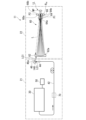
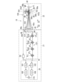
- FIG. 1 is a schematic diagram of a wavefront control device of a first embodiment according to the present invention
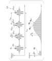
- FIG. FIG. 3 is a schematic diagram of an electric field distribution on the time axis (upper stage) and an intensity distribution on the frequency axis (lower stage) of an optical frequency comb
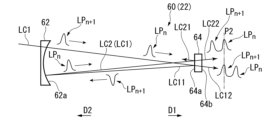
- 2 is a schematic diagram for explaining the principle of a wavefront synthesizing unit included in the wavefront control device shown in FIG. 1
- FIG. 3 is a schematic diagram for explaining how a wavefront synthesizing unit of the wavefront control device shown in FIG. 1 synthesizes wavefronts
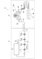
- It is a schematic diagram of a wavefront measurement system of a 2nd embodiment concerning the present invention.
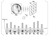
- FIG. 6 is a schematic diagram showing an example of a two-dimensional wavefront distribution of the wavefront measurement system shown in FIG. 5;
- FIG. It is a schematic diagram of a wavefront control device of a 2nd embodiment concerning the present invention.
- 8 is a schematic diagram showing an example of phase distribution of a plurality of optical pulses distributed on a predetermined plane of the wavefront control device shown in FIG. 7;
- FIG. FIG. 5 is a schematic diagram of a first modification of the wavefront control device according to the present invention;
- FIG. 5 is a schematic diagram of a second modification of the wavefront control device according to the present invention;
- FIG. 5 is a schematic diagram of a third modification of the wavefront control device according to the present invention;
- FIG. 11 is a schematic diagram for explaining how wavefront synthesis is performed in a wavefront synthesis section in a third modification of the wavefront control device according to the present invention;
- a wavefront control device 11 includes an optical frequency comb generation section 21 and a wavefront synthesis section 22 .
- the optical frequency comb generation unit 21 generates an optical frequency comb (hereinafter sometimes referred to as an optical comb) LC1 and outputs the generated optical frequency comb LC1 toward the wavefront synthesis unit 22 .
- the optical frequency comb generator 21 includes at least an optical frequency comb generator 30 and a phase controller 50, and further includes an optical fiber 42, a fiber collimator 44, and a plane mirror 46.
- the optical frequency comb generator 30 generates one optical frequency comb LC1 and emits it from the emission end.
- the optical frequency comb LC1 has a plurality of optical pulses LP 1 , LP 2 , . . . , LP n , LP n+1 , . is an optical pulse train spaced apart by . n is an arbitrary natural number and represents the number of optical pulses on the time axis.
- LP n , LP n+1 , . . . are collectively referred to as a plurality of optical pulses LPn.
- the optical frequency comb LC1 has a plurality of optical pulses LPn arranged in numerical order on the time axis.
- a plurality of optical pulses LPn have longitudinal mode information on the frequency axis.
- Each light pulse LPn has a predetermined frequency distribution. The frequency of each light pulse LPn changes continuously on the time axis.
- a plurality of light pulses LPn oscillate at a constant repetition time Trep .
- the optical frequency comb LC1 on the time axis shown in the upper part of FIG. 2 is Fourier transformed and observed on the frequency axis, as shown in the lower part of FIG. modes are observed. That is, the optical frequency comb LC1 has a plurality of frequency modes FM 1 , FM 2 , . . . FM m , FM m+1 , . have m is an arbitrary natural number and represents a number on the frequency axis of the spectrum.
- the interval between the centers of the frequency modes FM m and FM m+1 adjacent to each other on the frequency axis is the repetition frequency f rep .
- the repetition time T rep is represented by equation (2).
- Each of the plurality of light pulses LPn is composed of a superposition of many longitudinal modes propagating inside the resonator of the light source.
- the optical frequency comb LC1 which is an optical pulse train, is composed of a carrier wave (also called a carrier), which is a superimposed wave of longitudinal modes, and a wave packet forming its envelope (also called an envelope). Since the velocity of the carrier wave and the velocity of the wave packet are different from each other, a phase difference occurs over time.
- a phase difference ⁇ n+1 represented by Equation (3) is present between the optical pulses LP n and LP n+1 adjacent to each other on the time axis. occur.
- the offset time T ceo of the optical frequency comb LC1 is represented by Equation (4).
- the phase shift that is, the period of the phase difference ⁇ n+1 , is one cycle at the offset time T ceo .
- the center frequency fn of the n-th frequency mode of the optical frequency comb LC1 is expressed by Equation (5) using the repetition frequency frep and the offset frequency fceo .
- the phase relationship of the plurality of optical pulses LPn can be freely set and controlled.
- the repetition frequency f rep and the offset frequency f ceo are stabilized with atomic clock level accuracy and are precisely locked to their respective predetermined values with high accuracy.
- the optical frequency comb generator 30 is configured to be capable of emitting an optical comb and independently controlling the repetition frequency f rep and the offset frequency f ceo of the emitted optical comb, as will be described later.
- the configuration of the optical frequency comb generator 30 may be changed as appropriate as long as the optical comb can be emitted and controlled as described above.
- the optical frequency comb generator 30 is, for example, a mode-locked laser diode (MLLD) resonator equipped with an erbium (Er) doped fiber, a polarization controller, and a delay controller. It is configured.
- MLLD mode-locked laser diode
- Er erbium
- the optical frequency comb generator 30 may be composed of, for example, an add/drop straight waveguide made of quartz on a glass substrate and a ring waveguide connected between the straight waveguides.
- the optical frequency comb generator 30 may be composed of a ring-shaped resonator made of silicon nitride on a silicon (Si) substrate.
- the optical frequency comb generator 30 may be composed of a toroidal microresonator in which a flange is provided at the tip of a protrusion on a Si substrate.
- the optical frequency comb generator 30 may be composed of a crystal resonator.
- the phase control unit 50 is connected to the optical frequency comb generator 30 and controls the repetition frequency f rep and the offset frequency f ceo of the optical frequency comb LC1 emitted from the optical frequency comb generator 30. do.
- the phase controller 50 is connected to, for example, a function generator (not shown) included in the optical frequency comb generator 30 .
- the function generator feeds a high frequency signal to the resonators that produce the optical frequency comb LC1 in the optical frequency comb generator 30 and directly affects the repetition frequency f rep and the offset frequency f ceo of the optical frequency comb LC1.
- the phase control unit 50 is provided for manipulating the output of the high-frequency signal of the function generator, and is, for example, a computer connected to the function generator. The details of the control of the repetition frequency f rep and the offset frequency f ceo by the phase control unit 50 will be described later.
- the incident side end of the optical fiber 42 is connected to the optical frequency comb generator 30 .
- the fiber collimator 44 is connected to the exit end of the optical fiber 42 .
- the fiber collimator 44 collimates the optical frequency comb LC ⁇ b>1 propagating through the optical fiber 42 and emits it toward the reflecting surface 46 a of the plane mirror 46 .
- the plane mirror 46 reflects the optical frequency comb LC ⁇ b>1 incident on the reflecting surface 46 a toward the wavefront synthesis unit 22 .
- the plane mirror 46 is provided with an adjustment mechanism 146 capable of rotating the reflecting surface 46a.
- the adjustment mechanism 146 is, for example, a rotary stage having a rotating shaft extending vertically through the central portion of the reflecting surface 46a in plan view and a motor for rotating the rotating shaft.
- the adjusting mechanism 146 rotates the reflecting surface 46a in the direction of the arrow, the angle of the optical frequency comb LC1 emitted from the reflecting surface 46a toward the wavefront synthesizing unit 22 changes.
- the wavefront synthesizing unit 22 synthesizes the plurality of optical pulses LPn contained in the incident optical frequency comb LC1 at a position P1 in the direction of travel of the optical frequency comb LC1 (that is, a position on the optical path of the optical frequency comb LC1 and a plane mirror 46 position of the output surface 46b), the light pulses LPn are distributed to different positions according to the phase ⁇ n of each light pulse LPn.
- a predetermined wavefront is formed by mutual interference of the phases ⁇ n of the optical pulses LPn distributed to different positions POn.
- the phase ⁇ n of the optical pulse LP n is controlled by the ratio between the repetition frequency f rep of the optical position frequency comb and the offset frequency f ceo .
- the relationship of the phases ⁇ n of the plurality of light pulses LPn on the time axis is converted into the relationship of the positions where each of the plurality of light pulses LPn is irradiated at the position P1.
- a plurality of optical pulses LPn distributed to positions different from each other at a predetermined position P1 are wavefront-combined on the exit side of the position P1 to form a combined wavefront WP.
- the wavefront synthesizing unit 22 is configured by an MPC optical system 60 that configures, for example, a multipass cavity (MPC).
- the MPC optical system 60 has a concave mirror 62 and a plane mirror 64 .
- the concave mirror 62 is arranged at a position where the optical frequency comb LC1 reflected by the plane mirror 46 of the optical frequency comb generator 21 can be directly incident.
- the concave mirror 62 is arranged ahead of the reflecting surface 46a of the plane mirror 46 in the traveling direction of the optical frequency comb LC1.
- the plane mirror 64 is arranged in front of the concave mirror 62 in the traveling direction of the optical frequency comb LC1 that enters the wavefront synthesizing section 22 and passes through the concave mirror 62 .
- the plano-convex lens 66 is arranged in front of the plane mirror 64 in the traveling direction of the optical frequency comb LC1 that enters the wavefront synthesis unit 22 and passes through the concave mirror 62 .
- the concave mirror 62 has a reflecting surface 62a that specularly reflects substantially all of the incident optical frequency comb LC1.
- the plane mirror 64 has a reflecting surface 64a that mirror-reflects part of the incident optical frequency comb LC1 and transmits at least part of the rest.
- the reflecting surface 64a faces the reflecting surface 62a in the traveling direction of the optical frequency comb LC1 (that is, on the optical axis).
- the concave mirror 62 and the plane mirror 64 constitute a resonator.
- Each of the concave mirror 62, the plane mirror 64, and the plano-convex lens 66 is made of a material that can transmit the optical frequency comb LC1, such as quartz or optical glass.
- Each of the reflecting surfaces 62a and 64a is formed of a dielectric multilayer film or a metal deposition film in consideration of the wavelength of the optical frequency comb LC1 and the like so as to exhibit the above-described transmission characteristics.
- the inter-reflecting-surface distance L between the reflecting surface 62a of the concave mirror 62 and the reflecting surface 64a of the plane mirror 64 is represented by equations (6) and (7).
- c represents the speed of light
- L rep represents the inter-pulse distance of the optical frequency comb LC1.
- the optical frequency comb LC1 that has entered the MPC optical system 60 first passes through the concave mirror 62 and travels toward the reflecting surface 64a of the plane mirror 64 in the outgoing direction D1.
- the optical pulse LPn +1 follows the optical pulse LPn in time series with a repetition time Trep . Therefore, the light pulse LP n is first incident on the reflecting surface 64a, and the light pulse LP n+1 is incident after the repetition time T rep has elapsed.
- Part of the optical frequency comb LC11 incident on the reflecting surface 64a is specularly reflected and travels in the backward direction D2 having a component opposite to the forward direction D1. At least a portion of the remaining optical frequency comb LC12 of the optical frequency comb LC1 incident on the reflecting surface 64a is transmitted through the plane mirror 64 .
- the optical frequency comb LC11 is specularly reflected by the reflecting surface 64a of the concave mirror 62, travels in the forward direction D1 again as the optical frequency comb LC2, and enters the reflecting surface 64a of the plane mirror 64.
- a part of the optical frequency comb LC21 of the optical frequency comb LC2 that has entered the reflecting surface 64a is mirror-reflected and travels in the backward direction D2 again.
- At least a part of the remaining optical frequency comb LC22 incident on the reflecting surface 64a is transmitted through the plane mirror 64 .
- the optical frequency comb LC21 is specularly reflected by the reflecting surface 62a of the concave mirror 62, travels in the forward direction D1 again as an optical frequency comb LC3 (not shown), and enters the reflecting surface 64a of the plane mirror 64.
- the optical frequency comb LCk is branched into the optical frequency comb LCk1 and the optical frequency comb LCk2 at the reflecting surface 64a of the plane mirror 64, similarly to the optical frequency combs LC1 and LC2.
- k represents a natural number of 3 or more. As k increases, the light amount of the optical frequency comb LCk decreases. In the MPC optical system 60, the branching from the optical frequency comb LCk to the optical frequency combs LCk1 and LCk2 is repeated as described above until the light amount of the optical frequency comb LCk is almost exhausted.
- an exit surface 64b of the plane mirror 64 opposite to the reflecting surface 64a is a surface that intersects the traveling direction (optical axis) of the optical frequency comb LC1 and the central axis AX of the resonator. It is arranged at a predetermined position P1 in the traveling direction of the comb LC1.
- a central axis AX passes through each center of the concave mirror 62 and the plane mirror 64 .
- the plurality of optical frequency combs LCp2 are incident on different positions of the exit surface 64b, pass through the exit surface 64b, and enter the plano-convex lens 66 (not shown in FIG. 4).
- p represents a natural number.
- Each of the plurality of optical frequency combs LCp2 corresponds to the phase ⁇ n along the circumferential direction around the central axis AX on the exit surface 64b and is emitted from positions different from each other.
- a plurality of light pulses LPn are distributed to different positions according to their phases ⁇ n .
- a plurality of light pulses LPn are distributed at different positions POn corresponding to phases ⁇ n along the circumferential direction about the central axis AX. .
- the radius of the annular distribution around the central axis AX when the multiple light pulses LPn are distributed is the shortest on the exit surface 64 b of the plane mirror 64 .
- the MPC optical system 60 Since the MPC optical system 60 is composed of a passive optical system, no time is required for mechanical driving.
- the optical frequency comb LC1 reciprocates between the concave mirror 62 and the plane mirror 64 and is split by the reflecting surface 64a of the plane mirror 64. They are distributed substantially simultaneously to different positions POn on the exit surface 64b.
- the timing at which the optical frequency comb LC1 reaches the exit surface 64b is such that the light pulse LPn passes through each of the different positions POn on the exit surface 64b of the plane mirror 64 only by the phenomenon at the speed of light described above. deviates.
- a plurality of light waves LW 1 , LW 2 , . . . having phases ⁇ 1 , ⁇ 2 , . , LW n , LW n+1 , . . . are emitted simultaneously.
- a plurality of light waves LWn interfere with each other and emit a light wave LL having a combined wavefront WP as shown in FIG.
- the positions POn from which the plurality of optical pulses LPn are emitted are determined by the phase difference ⁇ n+1 between the optical frequency combs LCp2.
- the incident position of the optical frequency comb LCp2 on the exit surface 64b changes depending on the angle formed by the traveling direction of the optical frequency comb LCp, which is multiple-reflected between the concave mirror 62 and the plane mirror 64, with respect to the central axis AX as described above.
- the curvature of the reflecting surface 62a of the concave mirror 62 is designed in consideration of the incident position of the optical frequency comb LCp2 on the output surface 64b.
- the incident position of the optical frequency comb LCp2 on the exit surface 64b is set and controlled by the relationship of the phase ⁇ n of the optical pulse LPn of the optical frequency comb LC1, as will be described later.
- Equation (3) the pulse-to-pulse phase difference ⁇ n+1 is expressed as in Equation (3).
- the pulse-to-pulse phase difference ⁇ n+1 is constant for all n and becomes a constant phase difference ⁇ if the repetition frequency f rep and the offset frequency f ceo are perfectly controlled.
- Equation (9) holds for the phases ⁇ n and ⁇ n+1 of the plurality of light waves LW n and LW n+1 .
- the phase difference ⁇ n+1 between the light waves LW n and LW n+1 is determined only by two parameters, the repetition frequency f rep and the offset frequency f ceo of the optical frequency comb LC1.
- the phase difference ⁇ n+1 is ( ⁇ n+1 ⁇ n ). If the repetition frequency f rep and the offset frequency f ceo are perfectly controlled, the phase difference ⁇ n+1 is constant regardless of n.
- the optical pulses LP n and LP adjacent on the time axis of the optical frequency comb LC1 The phase difference ⁇ between n+1 can be controlled.
- a light wave LL having a combined wavefront WP dependent on the phase difference ⁇ whose repetition frequency f rep and offset frequency f ceo are controlled by the phase control unit 50 is emitted from the exit surface 64b of the plane mirror 64 arranged at the position P1. .
- the synthesized wavefront WP depends on the phase difference ⁇ for which the repetition frequency f rep and the offset frequency f ceo are controlled by the phase controller 50 .
- the plurality of optical frequency combs LCp2 are transmitted through the plane mirror 64 and enter the plano-convex lens 66 arranged in front of the plane mirror 64 in the traveling direction of the plurality of optical frequency combs LCp2.
- the plano-convex lens 66 has a convex surface 66a and a flat surface 66b.
- the plano-convex lens 66 is arranged to assist in adjusting the optical axis of each of the plurality of optical frequency combs LCp2 emitted from the plane mirror 64, adjusting the spread direction of the beam, and causing the plurality of optical frequency combs LCp2 to interfere with each other.
- a compound lens such as a camera lens may be arranged in an auxiliary manner in place of the plano-convex lens 66 .
- the plano-convex lens 66 may be omitted when there is no need to adjust the optical axis or the spread direction of the beams in order to cause the plurality of optical frequency combs LCp2 to interfere with each other.
- the wavefront control device 11 of the first embodiment includes the optical frequency comb generation section 21 and the wavefront synthesis section 22 .
- the optical frequency comb generator 21 emits an optical frequency comb LC1 having a plurality of optical pulses LPn arranged in numerical order on the time axis.
- the optical frequency comb generation unit 21 includes a phase control unit 50 that controls the repetition frequency f rep and the offset frequency f ceo of the optical frequency comb LC1.
- the wavefront synthesizing unit 22 converts each of the plurality of light pulses LPn of the optical frequency comb LC1 incident from the optical frequency comb generating unit 21 onto the plane 66b of the plano-convex lens 66 (the plane intersecting with the traveling direction of the optical frequency comb) into the first Distribute to different positions PO n according to the phase ⁇ n relative to the optical pulse LP 1 (not shown in FIG. 2).
- the wavefront synthesizing unit 22 generates a synthesized wavefront WP of the light pulses LPn emitted from mutually different positions.
- the wavefront control device 11 of the first embodiment if the two parameters of the optical frequency comb LC1; the repetition frequency f rep and the offset frequency f ceo are each controlled to a predetermined value by the phase control unit 50 in the optical frequency comb generation unit 21, , a plurality of light pulses LPn arranged in numerical order on the time axis before entering the wavefront synthesizing section 22 can be distributed to the plane 66b of the plano-convex lens 66, ie, the transverse mode, at the speed of light.
- each optical pulse LPn when a plurality of optical pulses LPn are distributed, each optical pulse LPn is controlled only by the repetition frequency f rep and the offset frequency f ceo regardless of the number of distributions. It can be put into a state with information of the phase ⁇ n .
- the plane 66b of the plano-convex lens 66 can emit a combined wavefront WP formed by interference between the light pulses LPn each having a phase ⁇ n .
- waveguide-type optical phased arrays and conventional radio-wave phased arrays which are conventional wavefront control methods
- optical waves or radio waves are branched more than the number of optical waves or radio waves to be phase-controlled (i.e., the number of distributions), or a plurality of A wave source is provided to control the phase of each of a plurality of light waves and radio waves.
- the wavefront control device 11 of the first embodiment is completely different from waveguide-type optical phased arrays and conventional radio wave phased arrays, and has two control parameters for one optical frequency comb LC1 ; By controlling only the phase ⁇ n of the light pulse LP n delivered to the plane 66b of the plano-convex lens 66 is controlled.
- the wavefront control device 11 of the first embodiment unlike the conventional wavefront control method, there is no need to individually phase-control a plurality of distributed optical signals (that is, optical pulses LPn). It is not necessary to arrange a phase control unit for controlling the phase of each optical signal. In the wavefront control device 11 of the first embodiment, there is no need to calibrate the plurality of phase control units. From these, according to the wavefront control device 11 of the first embodiment, the wavefront can be controlled at high speed by a simple control operation of controlling the repetition frequency f rep and the offset frequency f ceo regardless of the increase in the number of antennas. It can be carried out. According to the wavefront control device 11 of the first embodiment, miniaturization can be achieved without depending on an increase in the number of antennas.
- one optical frequency comb LC1 is used as the optical signal of the optical antenna.
- the optical frequency comb LC1 has a broadband spectral distribution, as illustrated in the lower part of FIG.
- the frequencies f m of each of the plurality of frequency modes FM m forming the spectral distribution of the optical frequency comb LC1, that is, the repetition frequency f rep and the offset frequency f ceo are controlled with high accuracy. be able to.
- the wavefront controller 11 of the first embodiment before the phases ⁇ n of the plurality of optical pulses LPn forming the composite wavefront WP (that is, the phases ⁇ n of the optical antennas) are distributed at the position P1, the optical frequency The comb generator 21 can control the repetition frequency f rep and the offset frequency f ceo with high accuracy at the atomic clock level.
- the wavefront control device 11 of the first embodiment since the optical frequency comb LC1 has a wide spectrum distribution composed of a plurality of frequency modes FM m , it is possible to easily widen the band of the light wave to be controlled.
- the wavelength of the optical frequency comb LC1 emitted from the optical frequency comb generator 30 is converted in the optical frequency comb generator 21, thereby facilitating further broadening of the band of the light wave to be controlled.
- the wavelength converter 70 may be arranged in the middle of the optical fiber 42 of the optical frequency comb generator 21 .
- the wavelength converter 70 may be incorporated in the optical frequency comb generator 30, or may be provided between the fiber collimator 44 and the plane mirror 46 in a region through which the optical frequency comb LC1 passes.
- the wavelength conversion unit 70 converts the spectral distribution of the optical frequency comb LC1 into a visible wavelength range or an ultraviolet wavelength range other than the near-infrared wavelength range. Equipped with materials and crystals that can be converted into The configuration of the wavelength conversion section 70 may be changed as appropriate. However, the relationship between the phases ⁇ n of the optical pulses LPn in the optical frequency comb LC1 emitted from the wavelength converter 70 is maintained.
- the wavefront control device 11 of the first embodiment by further including the wavefront conversion unit 70, it is possible to realize wavefront control and adaptive optics of ultrashort light pulses from the deep ultraviolet wavelength region to the terahertz (THz) region, for example. .
- THz terahertz
- the wavefront synthesizing unit 22 includes an MPC optical system (resonator structure) 60 having a concave mirror 62 and a plane mirror 64 (a pair of mirrors) facing each other.
- the reflecting surface 62a of the concave mirror 62 specularly reflects substantially all of the incident optical frequency comb LCp.
- a reflecting surface 64a of the plane mirror (one mirror) 64 reflects part of the incident optical frequency comb LCp and transmits at least part of the rest.
- the inter-reflecting surface distance L between the reflecting surface 62a of the concave mirror 62 and the reflecting surface 64a of the plane mirror 64 is represented by the formula (1) (that is, the formula (6)), and is given by the repetition frequency f rep of the optical frequency comb LC1. controlled.
- the optical frequency comb LC1 that has entered the MPC optical system 60 which is a passive optical system, is reciprocated between the reflecting surfaces 62a and 64a, and is simultaneously and traveling from the reflecting surface 64a. It is possible to emit optical frequency combs LCp2 in which the numbers n of the optical pulses LPn are shifted from each other at the same position in the direction.
- the plurality of light pulses LPn possessed by the optical frequency comb LC1 are emitted at the exit surface 64b of the plane mirror 64 and the plane 66b of the planoconvex lens 66 according to the phase ⁇ n without mechanical driving. They can be distributed to different locations.
- the wavefront control device 11 of the first embodiment has an adjustment mechanism 146 .
- the adjusting mechanism 146 adjusts the incident angle of the optical frequency comb LC1 incident on the reflecting surface 64a of the plane mirror 64 (at least one mirror) of the concave mirror 62 and the plane mirror 64 (a pair of mirrors). By adjusting the angle of the reflecting surface 46a of the plane mirror 46 using the adjusting mechanism 146, the angle of the optical frequency comb LC1 incident on the plane mirror 64 can be changed to control the combined wavefront WP.
- the reflecting surface 62a of the concave mirror 62 is concave with respect to the flat reflecting surface 64a of the plane mirror 64 and the flat surface 66b of the plano-convex lens 66 .
- the optical frequency comb LC1 emitted from the optical frequency comb generator 21 enters the MPC optical system 60 so as to be substantially orthogonal to the reflecting surface 64a.
- the optical frequency comb LCp resonates between the concave mirror 62 and the plane mirror 64, and collects light from the reflecting surface 62a toward the reflecting surface 64a.
- a plurality of light pulses LPn can be distributed in the condensing region R 64 of the reflecting surface 64b at appropriate intervals and arrangement at which the combined wavefront WP is preferably formed. .
- a plurality of light pulses LPn are distributed to different positions on the exit surface 64b of the plane mirror 64 according to the phase ⁇ n . can do.
- the cavity length of the MPC optical system 60 depends on the repetition frequency f rep of the optical frequency comb LC1.
- the repetition frequency f rep of the optical frequency comb used is about 10 MHz to 1000 MHz.
- the distance L between the reflecting surfaces of the MPC optical system 60 is about several tens cm to 1 m. .
- the distance L between the reflecting surfaces of the MPC optical system 60 is about 10 GHz to 100 GHz. In this case, the distance L between the reflecting surfaces of the MPC optical system 60 can be suppressed to about several cm to 10 cm.
- the adaptive optics device 12 of the second embodiment includes the wavefront control device 11 of the first embodiment and an imaging optical system 13.
- the same reference numerals as those of the wavefront control device 11 of the first embodiment are given to the configurations that are common to the configuration of the wavefront control device 11 of the first embodiment.
- the description of the contents common to the description of the wavefront control device 11 of the first embodiment will be omitted.
- FIG. 5 shows a schematic configuration of only the exit surface 64b of the plane mirror 64 of the wavefront synthesizing section 22 in the wavefront control device 11.
- the imaging optical system 13 is arranged in front of the traveling direction D3 of the light wave LL formed from the exit surface 64b.
- the imaging optical system 13 includes a beam splitter 102 , condensing lenses 104 and 106 and an imaging camera 110 .
- the adaptive optics device 12 measures the wavefront using the imaging camera 110, and takes a clear image of the object S to be measured when wavefront compensation is achieved. Wavefront measurement may be performed by a device other than the adaptive optics device 12 illustrated in FIG.
- the measured object S to be measured is arranged in front of the traveling direction D3 of the light wave LL from the exit surface 64b.
- the beam splitter 102 and the condenser lens 104 are sequentially arranged between the plane mirror 64 and the object S to be measured in the traveling direction D3.
- the condenser lens 104 is arranged between the beam splitter 102 and the object S to be measured in the traveling direction D3.
- the beam splitter 102 transmits the light wave LL emitted from the emission surface 64b and incident along the traveling direction D3.
- the condenser lens 104 is arranged behind the measurement position PX on the surface of or inside the object S to be measured by the focal length in the traveling direction D3.
- the beam splitter 102 has a reflecting surface 102a.
- the reflecting surface 102a transmits the light wave LL incident from the traveling direction D3.
- the reflective surface 102a mirror-reflects the light wave LW incident from the opposite direction and substantially parallel to the traveling direction D3 toward the traveling direction D4 that intersects with the traveling direction D3.
- a condensing lens 106 and an imaging camera 110 are sequentially arranged ahead of the beam splitter 102 in the traveling direction D4.
- the light wave LL emitted from the exit surface 64b of the plane mirror 64 passes through the beam splitter 102 and travels along the traveling direction D3.
- the wavefront WP 1 of the light wave LL in the imaging optical system 13 propagates the same wavefront WP 0 as the combined wavefront WP generated by combining a plurality of light pulses LPn emitted from each of the optical antennas on the emission surface 64b. This is the wavefront that reaches the imaging optical system 13 through the
- the light wave LL transmitted through the beam splitter 102 is condensed at the measurement position PX by the condensing lens 104 .
- the light wave LW reflected from the measurement position PX includes information on the light wave LL and information on the object S to be measured.
- the wavefront WP2 of the light wave LW is a wavefront that is changed by the action of the optical characteristics of the object S to be measured on the wavefront WP1 .
- the wavefront WP1 is an ideal plane wave
- the wavefront WP2 is scattered by the object S to be measured and becomes a distorted wavefront, and the imaging camera 110 captures a distorted image. If a known wavefront is generated by the wavefront control device 11 and the wavefront WP2 is photographed as a reflected image, the optical characteristics of the object S to be measured can be specified.
- the wavefront controller 11 If the wavefront controller 11 generates the wavefront WP1 that compensates for the optical characteristics, the wavefront WP2 , which is the object light, is adjusted, and the image of the object S to be measured obtained by the imaging camera 110 becomes clear.
- the light wave LW reflected from the object S to be measured enters the condensing lens 104, is collimated, and travels substantially parallel to and opposite to the travel direction D3.
- the light wave LW enters the beam splitter 102 in a direction substantially parallel to and opposite to the traveling direction D3, and is specularly reflected in the traveling direction D4 by the reflecting surface 102a.
- the light wave LW reflected by the reflecting surface 102a travels along the travel direction D4, is condensed by the condensing lens 106, and is received by the imaging camera 110.
- the wavefront WP2 of the light wave LW reflecting the optical characteristics of the object S to be measured travels in the direction substantially parallel to and opposite to the direction of travel D3
- the repetition frequency f rep and the offset frequency f ceo of the optical frequency comb LC1 are controlled by the phase control unit 50 of the wavefront controller 11 so as to obtain an orthogonal and substantially flat wavefront.
- the adaptive optics device 12 of the second embodiment described above includes the wavefront control device 11 of the first embodiment and the imaging optical system 13 .
- the imaging optical system 13 is configured to irradiate the object S to be measured with the light wave LL emitted from the wavefront control device 11 and to receive the light wave LW reflected or transmitted from the object S to be measured.
- the phase control unit 50 of the wavefront control device 11 controls only two control parameters of the optical frequency comb LC1 ;
- the wavefront WP1 of the light wave LL that irradiates the measurement object S can be freely controlled.
- the wavefront WP2 can be freely controlled.
- the repetition frequency f rep and the offset frequency f ceo of the optical frequency comb LC1 controlled using the information obtained from the light wave LW received by the imaging optical system 13 and the phase control unit 50 are
- the optical characteristics of the object S to be measured at the measurement position PX can be measured based on the relationship of .
- the wavefront WP2 of the light wave LW reflected or transmitted (reflected in FIG. 5) from the object S to be measured becomes a flat wavefront orthogonal to the optical axis.
- Only two control parameters of the optical frequency comb LC1 can be controlled by the phase controller 50 of the wavefront controller 11: the repetition frequency f rep and the offset frequency f ceo .
- the causal relationship between the wavefront WP1 of the light wave LL and the wavefront WP2 of the light wave LW and the optical characteristics of the object S to be measured at the measurement position PX is caused by the influence of air fluctuation, heat, etc. in the imaging optical system 13, for example. turbulence may occur.
- the wavefront WP2 is flattened, and the imaging camera 110 can acquire a high-contrast image and highly accurate measurement data.
- a plurality of phases ⁇ n of light are emitted from a plurality of positions POn acting as optical antennas to form wavefronts WP 0 .
- the adaptive optical device 12 of the second embodiment it is not necessary to individually control each of the phases ⁇ n of a plurality of lights as in the prior art.
- the wavefront WP2 of the light wave LW can be compensated.
- the wavelength conversion unit 70 is provided in the optical frequency comb generation unit 21 of the wavefront control device 11, so that the optical frequency comb LC1 in the stage preceding the installation position of the wavelength conversion unit 70 is Wavelength conversion is possible.
- adaptive optics can be realized with ultrashort pulses from the deep ultraviolet wavelength range to the THz range, for example.
- Adaptive optics using the adaptive optics device 12 of the second embodiment enables, for example, realization of direct fluorescence measurement with higher efficiency than conventional ones, or application to multiphoton absorption measurement and multiphoton microscopy.
- the adaptive optical device 12 of the second embodiment can be used for the purpose of evaluating the transverse mode characteristics of light waves in addition to the purpose of realizing adaptive optics as described above.
- a light emitting unit of a complicated optical system constituting an optical communication system, an optical functional device, or the like may be arranged to measure emitted light.
- the emitted light and the wavefront generated by the wavefront control device 11 may interfere with each other.
- the light wave LL emitted from the exit surface 64b of the plane mirror 64 at the position P1 is a two-dimensional plane that intersects the optical axis, and the repetition frequency f rep and the offset frequency f are controlled by the phase control unit 50.
- the bottom of FIG. 6 shows several pattern examples of two-dimensional wavefront distributions WD 1 , WD 2 , .
- the wavefront of the light wave LW reflected or transmitted from the light emitting part of the complicated optical system is received as it is without compensation, and the light intensity of the light wave LW is measured. You can see what kind of action the optical system received. From this, it is possible to know what kind of combination of simple wavefronts the light wave LW was generated, and to accurately evaluate the transverse mode characteristics of a complicated optical system or the like.
- two-dimensional wavefront distributions WD 1 , WD 2 . You can determine if it is included.
- the adaptive optics device 12 of the second embodiment suitably functions as a wavefront analyzer or two-dimensional spectroscope for evaluating transverse modes.
- a feedback mechanism 150 is provided in the wavefront control device 11 of the first embodiment.
- the feedback mechanism 150 includes a beam splitter 152 and a photodiode (PD) 154 .
- the beam splitter 152 is arranged in a region through which the optical frequency comb LCp2 passes between the plane mirror 64 and the plano-convex lens 66 of the wavefront synthesizing unit 22, and is arranged on the central axis AX between the plane mirror 64 and the plano-convex lens 66. there is
- the beam splitter 152 has a reflecting surface 152a.
- a portion of the optical frequency comb LCp2 incident on the beam splitter 152 is mirror-reflected by the reflecting surface 152a in a traveling direction D3 substantially perpendicular to the forward direction D1 and the backward direction D2.
- At least part of the remaining portion of the optical frequency comb LCp2 that has entered the beam splitter 152 passes through the reflecting surface 152a and enters the plano-convex lens 66 .
- a plurality of light pulses LPn are distributed to positions POn different from each other according to the phase ⁇ n .
- a light wave LL having a combined wavefront WP is emitted from an emission surface 64 b of the plane mirror 64 .
- the photodiode 154 receives the optical frequency comb LCp2 reflected by the reflecting surface 152a of the beam splitter 152 in the traveling direction D3.
- the photodiode 154 and the phase controller 50 of the optical frequency comb generator 21 are electrically connected by wire or wirelessly.
- the photodiode 154 outputs an electrical signal corresponding to the amount of light received from the optical frequency comb LCp2 to the phase controller 50 in real time.
- FIG. 7 shows only the repetition frequency control unit 161, the offset frequency control unit 162, the frequency dividers 165 and 166, and the mixer 170 of the device configuration of the optical frequency comb generation unit 21 of the wavefront control device 15.
- the repetition frequency control unit 161 receives the electrical signals obtained by the feedback mechanism 150 and the phase control unit 50, synchronizes with the distance L between the reflecting surfaces of the MPC optical system 60, and adjusts the repetition frequency f rep of the optical frequency comb LC1. Control.
- the offset frequency control unit 162 generates and controls the offset frequency f ceo of the optical frequency comb LC1.
- the repetition frequency f rep controlled by the repetition frequency control section 161 is input to the frequency divider 165 and divided into (1/ ⁇ ).
- the output from the offset frequency control section 162 is input to the frequency divider 166 and divided into (1/ ⁇ ). Outputs from frequency dividers 165 and 166 are input to mixer 170 and recursively input from mixer 170 to offset frequency control section 162 .
- the offset frequency control section 162 controls the offset frequency f ceo according to the recursively input signal.
- the offset frequency control section 162 controls the repetition frequency f rep so as to stabilize the MPC optical system 60 . If the phase control unit 50 operates to control the offset frequency f ceo with respect to the repetition frequency f rep , the frequency ratio between the repetition frequency f rep and the offset frequency f ceo can be controlled according to equation (10).
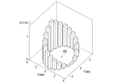
- FIG. 8 shows the result of numerical calculation of the phase distribution of the plurality of light pulses LPn distributed on the exit surface 64b of the plane mirror 64 of the wavefront synthesizing unit 22.
- the X-axis and the Y-axis in FIG. 8 represent two directions that are included in the output surface 64b when the origin is the position where the output surface 64b intersects the central axis AX, and are orthogonal to each other.
- the vertical axis in FIG. 8 represents the phase ⁇ n . As shown in FIG.
- a phase distribution is formed on the output surface 64b along the circumferential direction around the central axis AX.
- a plurality of phases ⁇ n of the phase distribution formed around the central axis AX continuously increase and decrease in the circumferential direction to form a virtual inclined plane.
- a light wave LL generated from the light pulse LPn is emitted in a direction substantially orthogonal to the inclined surface.
- the phase control unit 50 can freely and quickly control the phase distribution of the plurality of light pulses LPn on the exit surface 64b.
- the phase control unit 50 controls at least the repetition frequency f rep of the optical frequency comb LC1, and controls the ratio parameter ; , the inclined surface of the phase distribution of the plurality of light pulses LPn and the emission direction of the light waves LL on the emission surface 64b can be set freely and with high accuracy.
- a plurality of light pulses LPn are distributed by the MPC optical system 60 having the concave mirror 62 and the plane mirror 64.
- a phase distribution is formed in the circumferential direction around the central axis AX at 64b.
- a wavefront control device 15 of the third embodiment includes a feedback mechanism 150 .
- the feedback mechanism 150 is composed of a plurality of beams emitted from the plane mirror 64 and distributed to different positions according to the phase ⁇ n on the exit surface 64b. is fed back to the phase controller 50 of the optical frequency comb generator 21 .
- the phase control unit 50 compares the received intensity information of the optical pulses LPn of the plurality of optical frequency combs LCp2 with the known intensity information of the optical pulses LPn of the optical frequency comb LC1.
- the phase control unit 50 By using the phase control unit 50, it is possible to check in real time whether or not the phase distribution of the optical pulses LPn of the optical frequency comb LCp2 is fluctuating or disturbed due to environmental changes such as air fluctuations. Two parameters of the optical frequency comb LC1 in the optical frequency comb generation unit 21 using the phase control unit 50 when it is determined that there is fluctuation or disturbance in the phase distribution of the optical pulses LPn of the optical frequency comb LCp2; By controlling only the frequency f rep and the offset frequency f ceo , fluctuations and disturbances in the phase distribution can be eliminated. According to the wavefront control device 15 of the third embodiment, the repetition frequency f rep of the optical frequency comb LC1 can be synchronized with the cavity length of the MPC optical system 60 to stabilize the optical antenna.
- the wavefront control device 15 of the third embodiment can be applied to ultra-precise three-dimensional surveying by focal point scanning on a plane that intersects the traveling direction of the light wave LL and the central axis AX.
- the wavefront control device 15 of the third embodiment can be applied to ultra-precise three-dimensional surveying by absolute distance measurement in the traveling direction of the light wave LL and the depth direction substantially parallel to the central axis AX.
- the wavefront control device 15 of the third embodiment can be used to three-dimensionally scan the object S to be measured having a spherical surface, and the shortest distance to the spherical surface can be calculated by surface measurement.
- the Avogadro constant can be determined, for example, by profilometry of silicon spheres.
- three-dimensional LiDAR can be realized by performing measurement in the depth direction at the same time as scanning the focal point using the wavefront control device 15 of the third embodiment.
- the beam splitter 152 of the feedback mechanism 150 is arranged between the plane mirror 64 and the plano-convex lens 66 of the MPC optical system 60 .
- the beam splitter 152 may be arranged in a region through which the optical frequency comb LCp reflected by the reflecting surface 64a of the plane mirror 64 passes, as indicated by a two-dot chain line in FIG.
- the MPC optical system 60 having the concave mirror 62 and the plane mirror 64 is used. It changes circumferentially with respect to the time change in the circumferential direction. In order to stop the circular change, an inverted distribution obtained by inverting the phase distribution of the plurality of optical pulses LPn should be imparted to the phase distribution of the plurality of optical pulses LPn.
- the adaptive optics device 12 of the second embodiment may include the wavefront control device 15 of the third embodiment instead of the wavefront control device 11 of the first embodiment.
- the wavefront synthesizing unit of the wavefront control device according to the present invention may have a passive optical antenna structure other than the MPC optical system.
- a wavefront control device 17 shown in FIG. 9 and a wavefront control device 18 shown in FIG. 10 are given as first and second modifications of the wavefront control device according to the present invention.
- the optical frequency comb generator 21 of the wavefront controller 17 includes an optical frequency comb generator 30 , a phase controller 50 , an optical fiber 42 and an optical fiber coupler 180 .
- the wavefront synthesizing unit 22 of the wavefront control device 17 includes a plurality of output waveguides 182 instead of the MPC optical system 60 of the wavefront control devices 11 and 15 .
- the input side end of the optical fiber coupler 180 is connected to the output side end of the optical fiber 42 .
- the output side end of the optical fiber coupler 180 is connected to the input side ends of the plurality of output waveguides 182 .
- the plurality of output waveguides 182 are composed of output waveguides having different optical path lengths.
- the optical path length difference between the output waveguides 182 is equal to the optical path length difference when the optical pulses LP n and LP n+1 adjacent to each other on the time axis of the optical frequency comb LC1 propagate through the output waveguide 182 .
- the optical frequency combs LC1 whose numbers of the optical pulses LPn are different from each other are emitted at the same time.
- the wavefront control device 17 of the first modification similarly to the wavefront control devices 11 and 15, the plurality of optical pulses LPn of the optical frequency comb LC1 are shifted to different positions according to the phase ⁇ n without mechanical driving. It can be distributed to the output-side ends of a plurality of provided output waveguides 182 . According to the wavefront control device 17 of the first modified example, effects similar to those of the wavefront control devices 11 and 15 can be obtained.
- the optical frequency comb generator 21 of the wavefront controller 18 includes an optical frequency comb generator 30, a phase controller 50, and an optical fiber .
- the wavefront synthesizing unit 22 of the wavefront controller 18 includes an arrayed-waveguide grating (AWG) 190 instead of the MPC optical system 60 of the wavefront controllers 11 and 15 .
- the arrayed waveguide diffraction grating 190 includes an input waveguide 191 connected to the output-side end of the optical fiber 42, an input-side slab waveguide 192, an arrayed waveguide group 193, an output-side slab waveguide 194, and a plurality of output waveguides 195 .
- the optical frequency comb LC1 emitted from the optical fiber 42 is diffracted by the input-side slab waveguide 192 via the input waveguide 191, enters the arrayed waveguide group 193, and is independent for each waveguide of the arrayed waveguide group 193. propagating along the optical path.
- the optical path length difference between the waveguides of the arrayed waveguide group 193 corresponds to the optical path length difference when the optical pulses LP n and LP n+1 adjacent to each other on the time axis of the optical frequency comb LC1 propagate through the output waveguide 182. depends.
- the optical frequency comb LC1 emitted from the arrayed waveguide group 193 undergoes multiple interference in the output side slab waveguide 194, and converges on the incident side ends of the output waveguides 195 which are different for each wavelength.
- optical frequency combs LC1 whose numbers n of the optical pulses LPn are different from each other are emitted at the same time.
- a plurality of optical pulses LPn possessed by the optical frequency comb LC1 are shifted to different positions according to the phase ⁇ n without mechanical driving. It can be distributed to output ends of a plurality of provided output waveguides 195 . According to the wavefront control device 18 of the second modified example, effects similar to those of the wavefront control devices 11 and 15 can be obtained.
- a wavefront control device 81 shown in FIG. 11 there is a wavefront control device 81 shown in FIG. 11 in a wavefront control device 81, an intensity modulator (IM) 160 is provided in the wavefront control device 15 of the third embodiment.
- the intensity modulator 160 is arranged on the path of the optical frequency comb LC1 between the optical frequency comb generator 30 and the fiber collimator 44, and arranged in the middle of the optical fiber 42 of the optical frequency comb generator 21.
- the intensity modulator 160 thins out a predetermined optical pulse out of the plurality of optical pulses LPn of the optical frequency comb LC1 that are emitted from the optical frequency comb generator 30 and are incident via the optical fiber 42 .
- FIG. 11 an intensity modulator 160 is provided in the wavefront control device 15 of the third embodiment.
- the intensity modulator 160 is arranged on the path of the optical frequency comb LC1 between the optical frequency comb generator 30 and the fiber collimator 44, and arranged in the middle of the optical fiber 42 of the optical
- the intensity modulator 160 thins out the light pulses LC n+3 , LC n+6 , and LC n+7 out of the light pulses LC n+1 to LC n+8 which are part of the optical frequency comb LC1.
- predetermined light pulses out of the plurality of light pulses LPn of the optical frequency comb LC1 are thinned out by the intensity modulator 160, as shown in FIG. placement changes.
- the phase distribution formed on the exit surface 64b of the plane mirror 64 is a predetermined value based on the principle described with reference to FIG.
- the light wave LL generated from the optical frequency comb LC1 is emitted in a direction substantially perpendicular to the inclined plane of the phase distribution formed on the emission surface 64b.
- the plurality of light pulses LPn remaining after predetermined light pulses of the optical frequency comb LC1 are thinned out from the plane 66b of the plano-convex lens 66 in the wavefront synthesizing unit 22 interfere with each other.
- a composite wavefront WP consisting of For example, when the light pulses LC n+3 , LC n+6 and LC n +7 are thinned out by the intensity modulator 160 as shown in FIG.
- a composite wavefront WP generated by the interference of n+5 and LC n+8 is emitted.
- the wavefront WP 0 of the light wave LL ie, the two-dimensional wavefront distribution of the synthesized wavefront WP, is based on the light pulses remaining after predetermined light pulses are thinned out.
- a predetermined optical pulse to be thinned out by the intensity modulator 160 is calculated from the combined wavefront WP output from the wavefront combining section 22 and appropriately set. For this reason, in order to obtain a composite wavefront WP and a two-dimensional wavefront distribution of a specific transverse mode, the intensity modulator 160 modulates a specific transverse mode among the plurality of optical pulses LPn of the incident optical frequency comb LC1. thin out predetermined light pulses.
- the wavefront control device 81 of the third modification sends some of the optical pulses LCn of the optical frequency comb LC1 emitted from the optical frequency comb generator 21 to the wavefront synthesis unit 22. It has an intensity modulator 160 that emits towards. A portion of the optical pulse emitted from the intensity modulator 160 is obtained by back calculation from the desired transverse mode of the combined wavefront WP generated by the wavefront combining section 22 . According to the wavefront control device 81 of the third modified example, it is possible to generate and utilize a high-order transverse mode from a phase distribution having a high degree of freedom of control.
- the wavefront control device 81 of the third modified example can calculate the phase distribution that expresses the high-order transverse mode and control the phase distribution using the intensity modulator 160 .
- the wavefront control device 81 of the third modified example it is possible to appropriately find the correspondence between a plurality of phases ⁇ n emitted from a plurality of positions POn functioning as optical antennas. Further, by interfering not only with the synthesized wavefront WP formed by the thinned-out pulse train, but also with another synthesized wavefront WP that is subsequently formed, a more complicated high-order transverse mode can be formed.
- a resonator having the same resonator length as that of the MPC optical system 60 is arranged ahead of the plano-convex lens 66 in the traveling direction of the combined wavefront WP, and pulse stacking is performed using the resonator.
- the resonator placed in front of the MPC optical system 60 may be a spatial optical system such as the MPC optical system 60, or may be configured by an arrayed waveguide group, a bundle fiber in which a large number of fibers are bundled, or the like. .
Landscapes
- Physics & Mathematics (AREA)
- Nonlinear Science (AREA)
- General Physics & Mathematics (AREA)
- Optics & Photonics (AREA)
- Optical Modulation, Optical Deflection, Nonlinear Optics, Optical Demodulation, Optical Logic Elements (AREA)
Abstract
Priority Applications (4)
| Application Number | Priority Date | Filing Date | Title |
|---|---|---|---|
| US18/685,417 US20240393658A1 (en) | 2021-08-25 | 2022-08-24 | Wavefront control device and adaptive optics device |
| CN202280056897.2A CN117836705A (zh) | 2021-08-25 | 2022-08-24 | 波阵面控制装置以及补偿光学装置 |
| JP2023543952A JPWO2023027104A1 (fr) | 2021-08-25 | 2022-08-24 | |
| EP22861392.3A EP4394489A4 (fr) | 2021-08-25 | 2022-08-24 | Dispositif de commande de front d'onde et dispositif optique adaptatif |
Applications Claiming Priority (2)
| Application Number | Priority Date | Filing Date | Title |
|---|---|---|---|
| JP2021-137394 | 2021-08-25 | ||
| JP2021137394 | 2021-08-25 |
Publications (1)
| Publication Number | Publication Date |
|---|---|
| WO2023027104A1 true WO2023027104A1 (fr) | 2023-03-02 |
Family
ID=85322806
Family Applications (1)
| Application Number | Title | Priority Date | Filing Date |
|---|---|---|---|
| PCT/JP2022/031870 Ceased WO2023027104A1 (fr) | 2021-08-25 | 2022-08-24 | Dispositif de commande de front d'onde et dispositif optique adaptatif |
Country Status (5)
| Country | Link |
|---|---|
| US (1) | US20240393658A1 (fr) |
| EP (1) | EP4394489A4 (fr) |
| JP (1) | JPWO2023027104A1 (fr) |
| CN (1) | CN117836705A (fr) |
| WO (1) | WO2023027104A1 (fr) |
Families Citing this family (2)
| Publication number | Priority date | Publication date | Assignee | Title |
|---|---|---|---|---|
| EP4243209B1 (fr) * | 2022-03-09 | 2024-08-21 | Vaisala, OYJ | Appareil radar arrangé pour fonctionner dans des études météorologiques et/ou atmosphériques |
| CN118316534B (zh) * | 2024-06-11 | 2024-08-20 | 中国科学院国家授时中心 | 一种多用户光学频率分配系统及方法 |
Citations (6)
| Publication number | Priority date | Publication date | Assignee | Title |
|---|---|---|---|---|
| US9684076B1 (en) * | 2013-03-15 | 2017-06-20 | Daniel Feldkhun | Frequency multiplexed ranging |
| US20200081099A1 (en) * | 2017-04-17 | 2020-03-12 | Purdue Research Foundation | Ultrafast laser beam steering using frequency-arrayed optics |
| JP2020099048A (ja) * | 2018-12-18 | 2020-06-25 | タレス | 多波長光ビームをコヒーレントに再結合する装置及びシステム |
| JP2020112582A (ja) | 2019-01-07 | 2020-07-27 | 国立大学法人 東京大学 | 光照射装置、イメージング装置、及びレーザー加工装置 |
| CN213957609U (zh) * | 2020-11-13 | 2021-08-13 | 暨南大学 | 一种基于片上孤子频梳的无机械扫描的激光扫描装置 |
| JP2021137394A (ja) | 2020-03-06 | 2021-09-16 | 株式会社バンダイナムコエンターテインメント | コンピュータシステム、ゲームシステム、リプレイ動画提供方法及びプログラム |
Family Cites Families (6)
| Publication number | Priority date | Publication date | Assignee | Title |
|---|---|---|---|---|
| JP4771216B2 (ja) * | 2006-03-15 | 2011-09-14 | 独立行政法人情報通信研究機構 | 超平坦光周波数コム信号発生器 |
| JP5668265B2 (ja) * | 2009-03-16 | 2015-02-12 | 国立大学法人東京農工大学 | 光周波数コム発生装置および光周波数コム発生方法 |
| JP4949496B2 (ja) * | 2010-02-26 | 2012-06-06 | 住友大阪セメント株式会社 | 光周波数コム発生装置及びそれを用いた光パルス発生装置、並びに光周波数コム発生方法及びそれを用いた光パルス発生方法 |
| CN103633537B (zh) * | 2013-11-13 | 2016-09-14 | 中国科学院物理研究所 | 一种载波包络相移频率可控的低噪声光纤激光频率梳装置 |
| WO2019167476A1 (fr) * | 2018-03-02 | 2019-09-06 | 国立大学法人電気通信大学 | Procédé et dispositif d'acquisition d'intensité de signal d'interférence |
| US11011882B2 (en) * | 2018-09-05 | 2021-05-18 | Government Of The United States Of America, As Represented By The Secretary Of Commerce | Ultrafast electro-optic laser |
-
2022
- 2022-08-24 WO PCT/JP2022/031870 patent/WO2023027104A1/fr not_active Ceased
- 2022-08-24 CN CN202280056897.2A patent/CN117836705A/zh active Pending
- 2022-08-24 EP EP22861392.3A patent/EP4394489A4/fr active Pending
- 2022-08-24 JP JP2023543952A patent/JPWO2023027104A1/ja active Pending
- 2022-08-24 US US18/685,417 patent/US20240393658A1/en active Pending
Patent Citations (6)
| Publication number | Priority date | Publication date | Assignee | Title |
|---|---|---|---|---|
| US9684076B1 (en) * | 2013-03-15 | 2017-06-20 | Daniel Feldkhun | Frequency multiplexed ranging |
| US20200081099A1 (en) * | 2017-04-17 | 2020-03-12 | Purdue Research Foundation | Ultrafast laser beam steering using frequency-arrayed optics |
| JP2020099048A (ja) * | 2018-12-18 | 2020-06-25 | タレス | 多波長光ビームをコヒーレントに再結合する装置及びシステム |
| JP2020112582A (ja) | 2019-01-07 | 2020-07-27 | 国立大学法人 東京大学 | 光照射装置、イメージング装置、及びレーザー加工装置 |
| JP2021137394A (ja) | 2020-03-06 | 2021-09-16 | 株式会社バンダイナムコエンターテインメント | コンピュータシステム、ゲームシステム、リプレイ動画提供方法及びプログラム |
| CN213957609U (zh) * | 2020-11-13 | 2021-08-13 | 暨南大学 | 一种基于片上孤子频梳的无机械扫描的激光扫描装置 |
Non-Patent Citations (6)
| Title |
|---|
| H. ABEDIASL ET AL.: "Monolithic optical phased array transceiver in a standard SOI CMOS process", OPTICAL EXPRESS, vol. 23, no. 5, 2015, pages 6509 - 6519, XP055497279, DOI: 10.1364/OE.23.006509 |
| KATO TAKASHI; UCHIDA MEGUMI; TANAKA YURINA; MINOSHIMA KAORU: "One-shot three-dimensional imaging with a paired filter and chirped-frequency combs", 2018 CONFERENCE ON LASERS AND ELECTRO-OPTICS (CLEO), OSA, 13 May 2018 (2018-05-13), pages 1 - 2, XP033382016 * |
| M. C. SHIN ET AL.: "Chip-scale blue light phased array", OPTICS LETTERS, vol. 45, no. 7, 2020, pages 1934 - 1937 |
| NISHIYAMA, AKIKO; KOWZAN, GRZEGROZ; CHARCZUN, DOMINIK; SILVA DE OLIVEIRA, VINICIUS; RUEHL, AXEL; HARTL, INGMAR; TRAWINSKI, RYSZARD: "19p-C303-11 Highly sensitive measurement of CO-Ar using cavity-enhanced optical frequency comb spectroscopy", PROCEEDINGS OF THE 65TH JSAP SPRING MEETING 2018, JAPAN SOCIETY OF APPLIED PHYSICS; TOKYO; MARCH 17-20, 2018, vol. 65, 28 February 2018 (2018-02-28) - 20 March 2018 (2018-03-20), pages 03 - 548, XP009543922 * |
| See also references of EP4394489A4 |
| TSUDA, TAKUYA; MIZUNO, TAKAHIKO; MINAMIKAWA, TAKEO; YAMAMOTO, HIROTSUGU; YASUI, TAKESHI: "Implementation of imaging post amplifier on scan-less confocal dual-comb microscope", LASER-BASED MICRO- AND NANOPACKAGING AND ASSEMBLY II, SPIE, vol. 11140, 21 April 2019 (2019-04-21), pages 1114001 - 1114001-176, XP009543736, ISSN: 0277-786X * |
Also Published As
| Publication number | Publication date |
|---|---|
| EP4394489A1 (fr) | 2024-07-03 |
| EP4394489A4 (fr) | 2025-09-03 |
| CN117836705A (zh) | 2024-04-05 |
| JPWO2023027104A1 (fr) | 2023-03-02 |
| US20240393658A1 (en) | 2024-11-28 |
Similar Documents
| Publication | Publication Date | Title |
|---|---|---|
| TWI801364B (zh) | 用於提供啾頻光束之半導體光子電路及方法 | |
| JP6956964B2 (ja) | 光偏向デバイスおよびライダー装置 | |
| JP7076822B2 (ja) | 光受信器アレイ、及びライダー装置 | |
| US6570659B2 (en) | Broadband light source system and method and light source combiner | |
| WO2022062105A1 (fr) | Puce de télémétrie cohérente en réseau et son système | |
| US8497490B2 (en) | Terahertz wave generation device and method for generating terahertz wave | |
| US20220236416A1 (en) | Optical measurement device and optical measurement method | |
| CN110226103A (zh) | 环境空间轮廓估计 | |
| CN103712689A (zh) | 基于光学频率梳的连续激光器光谱线宽测量装置 | |
| US9007597B2 (en) | Microwave photonic true-time-delay | |
| WO2023027104A1 (fr) | Dispositif de commande de front d'onde et dispositif optique adaptatif | |
| US10837906B2 (en) | Measurement device and irradiation device | |
| US11314067B2 (en) | Illumination arrangement and method for illumination in a microscope and microscope | |
| JP6887350B2 (ja) | 光画像計測装置 | |
| JP2018045229A (ja) | 光源装置、およびそれを用いた情報取得装置 | |
| JP7194437B2 (ja) | 干渉信号強度取得方法及び干渉信号強度取得装置 | |
| JP2005317669A (ja) | テラヘルツ波発生装置及びそれを用いた計測装置 | |
| US7313299B2 (en) | Laser beam transformation and combination using tapered waveguides | |
| US20150276609A1 (en) | Light source apparatus and information-obtaining apparatus using the same | |
| JP2016029340A (ja) | 計測装置 | |
| JP7194438B2 (ja) | 2次元分光計測方法及び2次元分光計測装置 | |
| US20180073981A1 (en) | Light source apparatus, and information acquisition apparatus using the same |
Legal Events
| Date | Code | Title | Description |
|---|---|---|---|
| 121 | Ep: the epo has been informed by wipo that ep was designated in this application |
Ref document number: 22861392 Country of ref document: EP Kind code of ref document: A1 |
|
| WWE | Wipo information: entry into national phase |
Ref document number: 202280056897.2 Country of ref document: CN |
|
| WWE | Wipo information: entry into national phase |
Ref document number: 18685417 Country of ref document: US |
|
| WWE | Wipo information: entry into national phase |
Ref document number: 2023543952 Country of ref document: JP |
|
| WWE | Wipo information: entry into national phase |
Ref document number: 2022861392 Country of ref document: EP |
|
| NENP | Non-entry into the national phase |
Ref country code: DE |
|
| ENP | Entry into the national phase |
Ref document number: 2022861392 Country of ref document: EP Effective date: 20240325 |