WO2023089819A1 - 電力変換システム - Google Patents
電力変換システム Download PDFInfo
- Publication number
- WO2023089819A1 WO2023089819A1 PCT/JP2021/042772 JP2021042772W WO2023089819A1 WO 2023089819 A1 WO2023089819 A1 WO 2023089819A1 JP 2021042772 W JP2021042772 W JP 2021042772W WO 2023089819 A1 WO2023089819 A1 WO 2023089819A1
- Authority
- WO
- WIPO (PCT)
- Prior art keywords
- sub
- modules
- bus
- wall
- arm
- Prior art date
- Legal status (The legal status is an assumption and is not a legal conclusion. Google has not performed a legal analysis and makes no representation as to the accuracy of the status listed.)
- Ceased
Links
Images



Classifications
-
- H—ELECTRICITY
- H02—GENERATION; CONVERSION OR DISTRIBUTION OF ELECTRIC POWER
- H02M—APPARATUS FOR CONVERSION BETWEEN AC AND AC, BETWEEN AC AND DC, OR BETWEEN DC AND DC, AND FOR USE WITH MAINS OR SIMILAR POWER SUPPLY SYSTEMS; CONVERSION OF DC OR AC INPUT POWER INTO SURGE OUTPUT POWER; CONTROL OR REGULATION THEREOF
- H02M7/00—Conversion of AC power input into DC power output; Conversion of DC power input into AC power output
- H02M7/42—Conversion of DC power input into AC power output without possibility of reversal
- H02M7/44—Conversion of DC power input into AC power output without possibility of reversal by static converters
- H02M7/48—Conversion of DC power input into AC power output without possibility of reversal by static converters using discharge tubes with control electrode or semiconductor devices with control electrode
- H02M7/483—Converters with outputs that each can have more than two voltages levels
- H02M7/4835—Converters with outputs that each can have more than two voltages levels comprising two or more cells, each including a switchable capacitor, the capacitors having a nominal charge voltage which corresponds to a given fraction of the input voltage, and the capacitors being selectively connected in series to determine the instantaneous output voltage
-
- H—ELECTRICITY
- H02—GENERATION; CONVERSION OR DISTRIBUTION OF ELECTRIC POWER
- H02M—APPARATUS FOR CONVERSION BETWEEN AC AND AC, BETWEEN AC AND DC, OR BETWEEN DC AND DC, AND FOR USE WITH MAINS OR SIMILAR POWER SUPPLY SYSTEMS; CONVERSION OF DC OR AC INPUT POWER INTO SURGE OUTPUT POWER; CONTROL OR REGULATION THEREOF
- H02M5/00—Conversion of AC power input into AC power output, e.g. for change of voltage, for change of frequency, for change of number of phases
- H02M5/02—Conversion of AC power input into AC power output, e.g. for change of voltage, for change of frequency, for change of number of phases without intermediate conversion into DC
- H02M5/04—Conversion of AC power input into AC power output, e.g. for change of voltage, for change of frequency, for change of number of phases without intermediate conversion into DC by static converters
- H02M5/22—Conversion of AC power input into AC power output, e.g. for change of voltage, for change of frequency, for change of number of phases without intermediate conversion into DC by static converters using discharge tubes with control electrode or semiconductor devices with control electrode
- H02M5/225—Conversion of AC power input into AC power output, e.g. for change of voltage, for change of frequency, for change of number of phases without intermediate conversion into DC by static converters using discharge tubes with control electrode or semiconductor devices with control electrode comprising two stages of AC-AC conversion, e.g. having a high frequency intermediate link
-
- H—ELECTRICITY
- H02—GENERATION; CONVERSION OR DISTRIBUTION OF ELECTRIC POWER
- H02M—APPARATUS FOR CONVERSION BETWEEN AC AND AC, BETWEEN AC AND DC, OR BETWEEN DC AND DC, AND FOR USE WITH MAINS OR SIMILAR POWER SUPPLY SYSTEMS; CONVERSION OF DC OR AC INPUT POWER INTO SURGE OUTPUT POWER; CONTROL OR REGULATION THEREOF
- H02M7/00—Conversion of AC power input into DC power output; Conversion of DC power input into AC power output
- H02M7/003—Constructional details, e.g. physical layout, assembly, wiring or busbar connections
-
- H—ELECTRICITY
- H02—GENERATION; CONVERSION OR DISTRIBUTION OF ELECTRIC POWER
- H02M—APPARATUS FOR CONVERSION BETWEEN AC AND AC, BETWEEN AC AND DC, OR BETWEEN DC AND DC, AND FOR USE WITH MAINS OR SIMILAR POWER SUPPLY SYSTEMS; CONVERSION OF DC OR AC INPUT POWER INTO SURGE OUTPUT POWER; CONTROL OR REGULATION THEREOF
- H02M7/00—Conversion of AC power input into DC power output; Conversion of DC power input into AC power output
- H02M7/66—Conversion of AC power input into DC power output; Conversion of DC power input into AC power output with possibility of reversal
- H02M7/68—Conversion of AC power input into DC power output; Conversion of DC power input into AC power output with possibility of reversal by static converters
- H02M7/72—Conversion of AC power input into DC power output; Conversion of DC power input into AC power output with possibility of reversal by static converters using discharge tubes with control electrode or semiconductor devices with control electrode
- H02M7/75—Conversion of AC power input into DC power output; Conversion of DC power input into AC power output with possibility of reversal by static converters using discharge tubes with control electrode or semiconductor devices with control electrode using devices of a thyratron or thyristor type requiring extinguishing means
- H02M7/757—Conversion of AC power input into DC power output; Conversion of DC power input into AC power output with possibility of reversal by static converters using discharge tubes with control electrode or semiconductor devices with control electrode using devices of a thyratron or thyristor type requiring extinguishing means using semiconductor devices only
- H02M7/7575—Conversion of AC power input into DC power output; Conversion of DC power input into AC power output with possibility of reversal by static converters using discharge tubes with control electrode or semiconductor devices with control electrode using devices of a thyratron or thyristor type requiring extinguishing means using semiconductor devices only for high voltage direct transmission link
-
- H—ELECTRICITY
- H05—ELECTRIC TECHNIQUES NOT OTHERWISE PROVIDED FOR
- H05K—PRINTED CIRCUITS; CASINGS OR CONSTRUCTIONAL DETAILS OF ELECTRIC APPARATUS; MANUFACTURE OF ASSEMBLAGES OF ELECTRICAL COMPONENTS
- H05K7/00—Constructional details common to different types of electric apparatus
- H05K7/14—Mounting supporting structure in casing or on frame or rack
- H05K7/1422—Printed circuit boards receptacles, e.g. stacked structures, electronic circuit modules or box like frames
- H05K7/1427—Housings
- H05K7/1432—Housings specially adapted for power drive units or power converters
- H05K7/14325—Housings specially adapted for power drive units or power converters for cabinets or racks
-
- H—ELECTRICITY
- H05—ELECTRIC TECHNIQUES NOT OTHERWISE PROVIDED FOR
- H05K—PRINTED CIRCUITS; CASINGS OR CONSTRUCTIONAL DETAILS OF ELECTRIC APPARATUS; MANUFACTURE OF ASSEMBLAGES OF ELECTRICAL COMPONENTS
- H05K7/00—Constructional details common to different types of electric apparatus
- H05K7/14—Mounting supporting structure in casing or on frame or rack
- H05K7/1422—Printed circuit boards receptacles, e.g. stacked structures, electronic circuit modules or box like frames
- H05K7/1427—Housings
- H05K7/1432—Housings specially adapted for power drive units or power converters
- H05K7/14329—Housings specially adapted for power drive units or power converters specially adapted for the configuration of power bus bars
-
- H—ELECTRICITY
- H05—ELECTRIC TECHNIQUES NOT OTHERWISE PROVIDED FOR
- H05K—PRINTED CIRCUITS; CASINGS OR CONSTRUCTIONAL DETAILS OF ELECTRIC APPARATUS; MANUFACTURE OF ASSEMBLAGES OF ELECTRICAL COMPONENTS
- H05K7/00—Constructional details common to different types of electric apparatus
- H05K7/14—Mounting supporting structure in casing or on frame or rack
- H05K7/1422—Printed circuit boards receptacles, e.g. stacked structures, electronic circuit modules or box like frames
- H05K7/1427—Housings
- H05K7/1432—Housings specially adapted for power drive units or power converters
- H05K7/14339—Housings specially adapted for power drive units or power converters specially adapted for high voltage operation
Definitions
- the present disclosure relates to power conversion systems.
- a power conversion system that converts in the order AC, DC, AC is used to interchange power between two mainly independent, asynchronous AC power systems.
- This type of power conversion system is also called BTB (back-to-back) because the rectifier and the inverter are arranged with their backs to each other (for example, Japanese Patent Application Laid-Open No. 2009-507462 (Patent Document 1)).
- a BTB is used between a 50 Hz frequency AC power system and a 60 Hz frequency AC power system.
- a modular multilevel converter may be used as the forward converter and the inverse converter that constitute the above BTB.
- An MMC is provided with an arm for each phase of the AC power system, and each arm is constructed by cascading a large number of submodules.
- a submodule is a unit converter composed of a plurality of semiconductor switching elements and one or more capacitors. Furthermore, each arm is provided with a reactor to suppress circulating currents and fault currents.
- the power conversion system described above is high-voltage and large-capacity, it requires installation space and maintenance costs. Therefore, it is important how to arrange each sub-module and each reactor in consideration of the maintainability of the power conversion system.
- the present disclosure has been made in consideration of the above problems, and one of its purposes is to provide a power conversion system with excellent maintainability.
- a power conversion system that performs power conversion between a first AC power system and a second AC power system includes a positive side DC bus and a negative side DC bus, and respective phases and positive sides of the first AC power system. a plurality of first upper arms connected between the DC bus; a plurality of first lower arms connected between each phase of the first AC power system and the negative DC bus; a plurality of second upper arms connected between each phase of the second AC power system and the positive DC bus; and between each phase of the second AC power system and the negative DC bus. and a plurality of second lower arms.
- Each first upper arm, each first lower arm, each second upper arm, and each second lower arm are cascaded together and each unit converter converts alternating current power and direct current power.
- the power conversion system further includes a plurality of sub-modules in each of each first upper arm, each first lower arm, each second upper arm, and each second lower arm; It further comprises at least one storage chamber for storing the side DC bus.
- Each reactor of each first upper arm, each first lower arm, each second upper arm, and each second lower arm is provided outside the at least one storage chamber.
- a plurality of sub-modules constituting each upper arm and each lower arm are housed in at least one storage room, and each reactor is arranged outside the at least one storage room. It is possible to provide a power conversion system with excellent performance.
- FIG. 1 is a block diagram showing an electrical configuration of a power conversion system according to this embodiment
- FIG. FIG. 3 is a circuit diagram showing a configuration example of a sub-module that constitutes the power converter
- FIG. 4 is a perspective view showing a specific arrangement example of a plurality of sub-modules forming each arm
- 2 is a plan view showing the configuration of stage ST1.
- FIG. FIG. 2 is a plan view showing a specific arrangement example of the power conversion system 2 of FIG. 1
- 6 is a side view of a portion of a reactor 7UA of the U-phase upper arm 3UA of FIG. 5
- FIG. FIG. 6 is a side view of a portion of a plurality of submodules 20 (5UA) and a positive side DC bus 14P in FIG. 5;
- the Z direction indicates the vertical direction
- the X and Y directions indicate directions in the horizontal plane.
- the X direction and the Y direction do not necessarily have to be orthogonal, and may cross each other at an angle close to 90 degrees.
- the same reference numerals are given to the same or corresponding parts, and the description thereof will not be repeated.
- FIG. 1 is a block diagram showing the electrical configuration of the power conversion system of this embodiment.
- power conversion system 2 performs power conversion between first AC power system 1A and second AC power system 1B.
- the power conversion system 2 includes a first power conversion device 2A that performs power conversion between the AC power system 1A and the DC buses 14P and 14N, and a power conversion between the AC power system 1B and the DC buses 14P and 14N. and a second power conversion device 2B that performs
- power converter 2A is configured by a modular multilevel converter (MMC) including a plurality of submodules (SM) 20 cascaded with each other.
- MMC modular multilevel converter
- a “submodule” is also called a “converter cell” or a “unit converter”.
- the power conversion device 2A includes a U-phase upper arm 3UA and a U-phase lower arm 4UA corresponding to the U-phase of the AC power system 1A, a V-phase upper arm 3VA and a V-phase lower arm 4VA corresponding to the V-phase, and a W-phase. It includes corresponding W-phase upper arm 3WA and W-phase lower arm 3WB.
- U-phase upper arm 3UA includes a plurality of submodules 20 (5UA) and a reactor 7UA connected in series between positive DC bus 14P and U-phase AC terminal 9UA.
- U-phase lower arm 4UA includes a plurality of submodules 20 (6UA) and a reactor 8VB connected in series between negative DC bus 14N and U-phase AC terminal 9UA.
- V-phase upper arm 3VA includes a plurality of sub-modules 20 (5VA) and a reactor 7VA connected in series between positive DC bus 14P and V-phase AC terminal 9VA.
- V-phase lower arm 4VA includes a plurality of sub-modules 20 (6VA) and a reactor 8VB connected in series between negative DC bus 14N and V-phase AC terminal 9VA.
- W-phase upper arm 3WA includes a plurality of submodules 20 (5WA) and a reactor 7WA connected in series between positive DC bus 14P and W-phase AC terminal 9WA.
- W-phase lower arm 4WA includes a plurality of sub-modules 20 (6WA) and a reactor 8VB connected in series between negative DC bus 14N and W-phase AC terminal 9WA.
- upper arm 3A and lower arm 4A When collectively referring to the upper arm and the lower arm or when indicating an arbitrary phase, they are referred to as upper arm 3A and lower arm 4A.
- a plurality of sub-modules 5A, 6A are used when collectively referring to the plurality of sub-modules of the upper arm and the plurality of sub-modules 20 of the lower arm or when referring to any one.
- Reactors 7A and 8A are used to collectively refer to the reactors of the upper arm and the reactors of the lower arm or to indicate arbitrary reactors.
- the reactor 7A is connected between the AC terminal 9A and the plurality of submodules 5A, and the reactor 8A is connected between the reactor 8A and the plurality of submodules 6A. That is, reactors 7A and 8A are arranged close to AC terminal 9A (that is, away from positive DC bus 14P or negative DC bus 14N). The reason for this is to consider the maintainability of the power conversion system 2, and the details will be described later with reference to FIG.
- the power converter 2A further includes a transformer 13A and an initial charging resistor 10A.
- the transformer 13A is connected between the AC power system 1A and AC terminals 9UA, 9VA, and 9WA (collectively referred to as AC terminals 9A).
- AC terminals 9A instead of using the transformer 13A in FIG. 1, a configuration may be adopted in which the AC power system 1A and the power converter 2A are connected via a grid reactor.
- the initial charging resistor 10A includes a resistor 11 connected in series to each of the U-phase, V-phase, and W-phase lines of the AC power system 1A, and a switch 12 connected in parallel with each resistor.
- the charging current flowing through the submodule 20 is suppressed by opening each switch 12 .
- resistor 11 is bypassed by closing switch 12 .
- the initial charging resistor 10A may be provided on either the primary side (that is, the AC power system 1A side) or the secondary side (that is, the AC terminal 9A side) of the transformer 13A. By providing the initial charging resistor 10A on the primary side of the transformer 13A, the inrush current flowing from the AC power system 1A to the transformer 13A can be suppressed.
- FIG. 2 is a circuit diagram showing a configuration example of a sub-module configuring the power converter.
- the sub-module 20 shown in (A) of FIG. 2 has a circuit configuration called a half-bridge configuration.
- This submodule 20 includes a series body formed by connecting two switching elements 21P and 21N in series, a storage element 22, and input/output terminals T1 and T2.
- the series body of switching elements 21P and 21N and storage element 22 are connected in parallel. Both terminals of the switching element 21N are connected to the input/output terminals T1 and T2, respectively.
- a half bridge circuit is configured by switching elements 21P and 21N.
- the submodule 20 outputs the voltage of the storage element 22 or zero voltage between the input/output terminals T1 and T2 by switching operations of the switching elements 21P and 21N.
- the switching element 21P is turned on and the switching element 21N is turned off
- the voltage of the storage element 22 is output from the submodule 20 .
- the switching element 21P is turned off and the switching element 21N is turned on
- the submodule 20 outputs zero voltage.
- the submodule 20 shown in FIG. 2(B) has a circuit configuration called a full bridge configuration.
- the submodule 20 includes a first series body formed by connecting two switching elements 21P1 and 21N1 in series, a second series body formed by connecting two switching elements 21P2 and 21N2 in series, It has a power storage element 22 and input/output terminals T1 and T2.
- the first series body, the second series body, and the storage element 22 are connected in parallel.
- a midpoint of switching element 21P1 and switching element 21N1 is connected to input/output terminal T1.
- the midpoint of switching element 21P2 and switching element 21N2 is connected to input/output terminal T2.
- a full bridge circuit 25 is configured by the switching elements 21P1, 21N1, 21P2, and 21N2.
- the submodule 20 converts the voltage of the storage element 22, the voltage obtained by inverting the sign of the voltage of the storage element 22, or zero voltage to the input/output terminals T1 and T2 by switching operations of the switching elements 21P1, 21N1, 21P2, and 21N2. output between
- each of the switching elements 21P, 21N, 21P1, 21N1, 21P2, and 21N2 is, for example, an IGBT (Insulated Gate Bipolar Transistor), a GCT (Gate Commutated Turn-off) thyristor, or the like.
- An FWD Freewheeling Diode is connected in anti-parallel to a self-arc-extinguishing semiconductor switching element.
- capacitors such as film capacitors are mainly used for the storage element 22 .
- the storage element 22 may also be referred to as a capacitor in the following description.
- the input/output terminal T1 is connected to the input/output terminal T2 of the adjacent submodule 20 or the positive side DC bus 14P.
- the input/output terminal T2 is connected to the input/output terminal T1 of the adjacent submodule 20 or the AC terminals 9A and 9B.
- the input/output terminal T1 is connected to the input/output terminal T2 of the adjacent submodule 20 or the AC terminals 9A and 9B. is connected to the input/output terminal T1 of the submodule 20 or the negative side DC bus 14N.
- each sub-module 20 is housed in a plurality of insulating containers stacked in a tower.
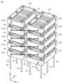
- FIG. 3 is a perspective view showing a specific arrangement example of a plurality of submodules that constitute each arm.
- An arrangement example of a plurality of sub-modules 20 (5UA) constituting the U-phase upper arm 3UA will be described below, but the same applies to other arms.
- Racks LK1 and LK2 are arranged adjacent to each other in the X direction in the figure.
- the stages ST1 to ST5 are sequentially arranged in the Z direction (height direction) in the figure and arranged parallel to each other.
- the first stage ST1 is supported on the floor by six pillars 35 .
- Stages ST2-ST5 are supported by six columns 36 on stages ST1-ST4, respectively.
- the stages ST11 to ST15 are sequentially arranged in the Z direction (height direction) in the figure and arranged parallel to each other.
- the first stage ST11 is supported on the floor by six supports 35 .
- Stages ST12 to ST15 are supported by six columns 36 on stages ST11 to ST14, respectively.
- Stages ST11 to ST15 of rack LK2 are arranged at the same height as stages ST1 to ST5 of rack LK1, respectively.
- FIG. 4 is a plan view showing the configuration of the stage ST1.
- the stage ST1 includes a rectangular substrate 31, six insulators 32, an insulating shield 33, a positive terminal T11, and a negative terminal T12.
- the short side of the substrate 31 is oriented in the X direction in the drawing, and the long side is oriented in the Y direction in the drawing.
- Six holes are formed in the peripheral portion of the substrate 31 , six insulators 32 are fitted into the six holes, respectively, and the central portion of each insulator 32 is fixed to the substrate 31 .
- a hole for fitting a support 35 or 36 is drilled in the upper end and lower end of each insulator 32 .
- the periphery of the substrate 31 is covered with an insulating shield 33 .
- the insulating shield 33 is divided into four portions corresponding to the four sides of the substrate 31, and each portion is fixed to the substrate 31 by a fixing member (not shown).
- a positive terminal T11 first terminal
- a negative terminal T11 second terminal
- the positive terminal T11, the eight sub-modules 20, and the negative terminal T12 are arranged in the Y direction in the drawing.
- the positive terminal T11 penetrates the insulating shield 33 and protrudes toward the front side of the stage ST1.
- the negative terminal T12 penetrates the insulating shield 33 and protrudes toward the rear side of the stage ST1.
- Eight submodules 20 are cascaded between terminals T11 and T12.
- Input/output terminals T1 and T2 of adjacent sub-modules 20 are connected to each other by a metal plate EL.
- Each of the other stages ST2 to ST5 of rack LK1 has the same configuration as stage ST1.
- the positive terminal T11, the eight sub-modules 20, and the negative terminal T12 are arranged in the direction opposite to the Y direction in the figure.
- the positive terminal T11 penetrates the insulating shield 33 and protrudes to the rear side of the stage ST11.
- the negative terminal T12 penetrates the insulating shield 33 and protrudes toward the front side of the stage ST11.
- Eight submodules 20 are cascaded between terminals T11 and T12.
- each sub-module 20 is connected in series.
- the terminal T11 of the stage ST1 is the terminal on the highest potential side.
- a terminal T12 of the stage ST1 and a terminal T11 of the stage ST11 are connected by a wiring 37.
- FIG. Terminal T12 of stage ST11 and terminal T11 of stage ST2 are connected by wiring 37 .
- Terminal T12 of stage ST2 and terminal T11 of stage ST12 are connected by wiring 37 .
- Stages ST12, ST3, ST13, ST4, ST14, ST5, ST5, and ST15 are spirally connected in this order.
- the terminal T12 of the stage ST15 is the terminal on the lowest potential side.
- FIG. 1 [Planar layout of power conversion system] A practical arrangement example of the power conversion system 2 of FIG. 1 will be described below with reference to FIGS. 5 to 7. FIG. Each component of the power conversion system 2 is arranged in consideration of maintainability.
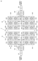
- FIG. 5 is a plan view showing a specific arrangement example of the power conversion system 2 of FIG.
- the walls 41-44 defining the storage chamber 40 are shown in cross section.
- a plurality of sub-modules 20 (5UA, 5VA, 5WA) of upper arm 3A constituting power converter 2A of FIG. 1 and a plurality of sub-modules 20 of upper arm 3B constituting power converter 2B.
- (5UB, 5VB, 5WB) and the positive side DC bus line 14P connecting them are arranged in the storage room 40.
- a plurality of sub-modules 20 (6UA, 6VA, 6WA) of the lower arm 4A constituting the power conversion device 2A and a plurality of sub-modules 20 (6UB, 6VB, 6WB) of the lower arm 4B constituting the power conversion device 2B , and the negative side DC bus 14N that connects them are arranged inside the storage room 40 .
- the plurality of submodules 20 forming each arm are stacked in a tower shape.
- the positive side DC bus 14P and the negative side DC bus 14N are arranged extending in the Y direction in FIG. 5 in plan view.
- positive side DC bus 14P and negative side DC bus 14N do not have to extend in exactly the same direction.
- the plurality of sub-modules 20 (5UA, 5VA, 5WA) of the upper arm 3A constituting the power conversion device 2A and the plurality of sub-modules 20 (5UB, 5VB, 5WB) of the upper arm 3B constituting the power conversion device 2B? , are arranged opposite to each other with respect to the positive DC bus 14P.
- a plurality of sub-modules 20 (6UA, 6VA, 6WA) of the lower arm 4A constituting the power conversion device 2A and a plurality of sub-modules 20 (6UB, 6VB, 6WB) of the lower arm 4B constituting the power conversion device 2B ) are arranged opposite to each other with respect to the negative DC bus 14N.
- the plurality of sub-modules 20 of each arm constituting the power conversion device 2A and the sub-modules 20 of the corresponding arms constituting the power conversion device 2B are arranged side by side in the X direction intersecting the Y direction. be.
- the floor surface of the storage room 40 includes a first area and a second area.
- the floor surface of the storage room 40 is divided into a first area 49P and a second area 49N at the position of the two-dot chain line of reference numeral 57.
- the first region 49P there are a plurality of sub-modules 20 (5UA, 5VA, 5WA) of the upper arm 3A constituting the power conversion device 2A and a plurality of sub-modules 20 (5UA, 5VA, 5WA) of the upper arm 3B constituting the power conversion device 2B.
- 5UB, 5VB, 5WB and the positive side DC bus 14P are arranged.
- a plurality of sub-modules 20 (6UA, 6VA, 6WA) of the lower arm 4A constituting the power conversion device 2A and a plurality of sub-modules 20 (6UA, 6VA, 6WA) of the lower arm 4B constituting the power conversion device 2B ( 6UB, 6VB, 6WB) and a negative side DC bus 14N.
- the plurality of sub-modules 20 (5UA, 5VA, 5WA) of the upper arm 3A that constitute the power converter 2A are arranged between the wall 41 defining the storage room 40 and the positive DC bus 14P.
- a plurality of sub-modules 20 (5UB, 5VB, 5WB) of the upper arm 3B constituting the power converter 2B are arranged between a wall 42 defining a storage room 40 and facing the wall 41 and the positive DC bus 14P. be.
- a plurality of sub-modules 20 (6UA, 6VA, 6WA) of the lower arm 4A that constitute the power converter 2A are arranged between the wall 41 and the negative side DC bus 14N.
- a plurality of sub-modules 20 (6UB, 6VB, 6WB) of the lower arm 4B that constitute the power conversion device 2B are arranged between the wall 42 and the negative side DC bus 14N.
- a current transformer 46P for DC current detection, a voltage transformer 47P for DC voltage detection, and a DC lightning arrester 48P are connected to the positive DC bus 14P.
- a current transformer 46N for DC current detection, a voltage transformer 47N for DC voltage detection, and a DC lightning arrester 48N are connected to the negative DC bus 14N.
- Air adjusted to the set temperature range and the set room temperature range by the air conditioner 54 is supplied to the storage room 40 via the duct 55 . Furthermore, the inside of storage room 40 may be made more clean than the outside of storage room 40 by providing a dust filter at the blower port of air conditioner 54 . In order to improve the cleanliness of the interior of the storage room 40 in this manner, the air pressure inside the storage room 40 is set higher than the air pressure outside the storage room 40 .
- Reactors 7UA, 7VA, 7WA, 8UA, 8VA, and 8WA constituting power converter 2A and reactors 7UB, 7VB, 7WB, 8UB, 8VB, and 8WB constituting power converter 2B are stored outside storage room 40. They are arranged opposite each other with respect to the chamber 40 .
- the reactors 7UA, 7VA, 7WA, 8UA, 8VA, and 8WA constituting the power converter 2A are provided with a plurality of corresponding submodules 5UA, 5VA, It is arranged adjacent to 5WA, 6UA, 6VA and 6WA.
- the reactors 7UA, 7VA, 7WA, 8UA, 8VA, 8WA are connected to a plurality of corresponding submodules 5UA, 5VA, 5WA, 6UA via through bushings 51UA, 51VA, 51WA, 52UA, 52VA, 52WA penetrating the wall 41, respectively. , 6VA and 6WA, respectively.
- the reactors 7UB, 7VB, 7WB, 8UB, 8VB, and 8WB constituting the power conversion device 2B are provided with a plurality of corresponding sub-sub reactors with a wall 42 (opposed to the wall 41) that defines the storage chamber 40 interposed therebetween. It is arranged adjacent to modules 5UB, 5VB, 5WB, 6UB, 6VB and 6WB.
- the reactors 7UB, 7VB, 7WB, 8UB, 8VB, 8WB are connected to a plurality of corresponding submodules 5UB, 5VB, 5WB, through bushings 51UB, 51V1, 51WB, 52UB, 52VB, 52WB that penetrate the wall 42, respectively. 6UB, 6VB and 6WB are connected respectively.
- the reactors 7UA, 7VA, 7WA, 8UA, 8VA, and 8WA that make up the power converter 2A are connected to the AC bus 53A, and connected to the initial charging resistor 10A and the transformer 13A via the AC bus 53A.
- reactors 7UB, 7VB, 7WB, 8UB, 8VB, and 8WB constituting power converter 2B are connected to AC bus 53B, and connected to initial charging resistor 10B and transformer 13B via AC bus 53B.
- AC buses 53A and 53B extend in the Y direction.
- the AC bus 53A is arranged outside the storage room 40 along the wall 41 and its extending direction
- the AC bus 53B is arranged outside the storage room 40 along the wall 42 and its extending direction.
- Reactors 7UA, 7VA, 7WA, 8UA, 8VA, and 8WA are arranged between AC bus 53A and storage chamber 40 .
- Reactors 7UB, 7VB, 7WB, 8UB, 8VB, and 8WB are arranged between AC bus 53B and storage chamber 40 .
- a plurality of sub-modules 20 (5UA, 5VA, 5WA, 5UB, 5VB, 5WB) and a positive side DC bus 14P related to the upper arms 3A and 3B, and a plurality of modules related to the lower arms 4A and 4B.
- Submodules 20 (6UA, 6VA, 6WA, 6UB, 6VB, 6WB) and negative side DC bus 14N are arranged separately in the Y direction. Therefore, the storage room 40 is separated in the Y direction by the wall 57 extending in the X direction, and the components related to the upper arms 3A and 3B and the components related to the lower arms 4A and 4B are separated into separate rooms. You can store it.
- the power conversion system of the modified example includes a first storage room and a second storage room.
- the first storage room corresponds to the portion having the floor surface 49P, the wall 43, the wall 57, the first wall (the portion of the wall 41 that rises from the floor surface 49P) and the second wall. (the portion of the wall 42 that rises from the floor surface 49P).
- the first wall and the second wall face each other.
- the second storage room corresponds to the portion having the floor surface 49N, the wall 44, the wall 57, the third wall (the portion of the wall 41 that rises from the floor surface 49N) and the fourth wall (the floor surface of the wall 42). 49N).
- the third wall is positioned in the extending direction of the first wall
- the fourth wall is positioned in the extending direction of the second wall.
- the third wall and the fourth wall face each other.
- the first storage room contains a plurality of submodules 20 (5UA, 5VA, 5WA) of the upper arm 3A that constitutes the power converter 2A, and a plurality of submodules 20 (5UA, 5VA, 5WA) of the upper arm 3B that constitutes the power converter 2B.
- Submodules 20 (5UB, 5VB, 5WB) and positive side DC bus 14P are accommodated.
- a plurality of sub-modules 20 (6UA, 6VA, 6WA) of the lower arm 4A constituting the power converter 2A and a plurality of sub-modules 20 (6UA, 6VA, 6WA) of the lower arm 4B constituting the power converter 2B are provided.
- a plurality of sub-modules 20 (5UA, 5VA, 5WA) of upper arm 3A are arranged between the first wall and positive side DC bus 14P.
- a plurality of sub-modules 20 (5UB, 5VB, 5WB) of upper arm 3B are arranged between the second wall and positive side DC bus 14P.
- a plurality of sub-modules 20 (6UA, 6VA, 6WA) of the lower arm 4A are arranged between the third wall and the negative side DC bus 14N.
- a plurality of sub-modules 20 (6UB, 6VB, 6WB) of the lower arm 4B are arranged between the fourth wall and the negative DC bus 14N.
- the reactors 7UA, 7VA, 7WA that constitute the upper arm 3A of the power converter 2A are arranged adjacent to the corresponding plurality of sub-modules 5UA, 5VA, 5WA with the first wall interposed therebetween.
- the reactors 7UA, 7VA, 7WA are respectively connected to the plurality of corresponding submodules 5UA, 5VA, 5WA via through bushings 51UA, 51VA, 51WA penetrating through the first wall.
- the reactors 7UB, 7VB, 7WB that constitute the upper arm 3B of the power conversion device 2B are arranged adjacent to the corresponding plurality of sub-modules 5UB, 5VB, 5WB with the second wall interposed therebetween.
- the reactors 7UB, 7VB, 7WB are connected to the corresponding plurality of submodules 5UB, 5VB, 5WB via through bushings 51UB, 51VB, 51WB penetrating through the second wall, respectively.
- the reactors 8UA, 8VA, 8WA that constitute the lower arm 4A of the power conversion device 2A are arranged adjacent to the corresponding plurality of sub-modules 6UA, 6VA, 6WA with the third wall interposed therebetween.
- the reactors 8UA, 8VA, 8WA are connected to the corresponding sub-modules 6UA, 6VA, 6WA via through bushings 52UA, 52VA, 52WA that penetrate the third wall, respectively.
- the reactors 8UB, 8VB, 8WB that constitute the lower arm 4B of the power conversion device 2B are arranged adjacent to the corresponding plurality of sub-modules 6UB, 6VB, 6WB with the fourth wall interposed therebetween.
- the reactors 8UB, 8VB, 8WB are connected to the corresponding sub-modules 6UB, 6VB, 6WB via through bushings 52UB, 52VB, 52WB penetrating through the fourth wall, respectively.
- FIG. 6 is a side view of the reactor 7UA portion of the U-phase upper arm 3UA of FIG.
- the wall surface 41 defining the storage room 40, the floor portion, and the AC bus 53A are shown in cross section.
- the reactor 7UA is supported by insulator-equipped struts 71 attached to a frame 70 on the floor surface 65 .
- a first terminal 72 of reactor 7UA is connected to through bushing 51UA via wiring 62 (for example, an aluminum stranded wire).
- Through bushing 51UA is fixed to wall 41 by flange 69 .
- a second terminal 73 of reactor 7UA is connected to AC bus 53A via wiring 63 and bushing 74 .
- AC bus 53A is, for example, a gas-tight bus.
- AC bus 53A is supported by pedestal 75 .
- a current transformer 76 for detecting an alternating current (arm current) is provided between the bushing 74 and the AC bus 53A.
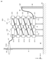
- FIG. 7 is a side view of the multiple sub-modules 20 (5UA) and the positive side DC bus 14P of FIG.
- the wall surface 41 defining the storage chamber 40, the floor portion, and the positive side DC bus 14P are shown in cross section.
- the positive DC bus 14P is supported on the floor surface 65 by a support 80 with an insulator.
- a plurality of submodules 5UA are stacked in a tower shape as described with reference to FIGS.
- Terminal T11 of stage ST1 which has the highest potential in racks LK1 and LK2, is connected to positive side DC bus 14P via wiring 60 (for example, aluminum twisted wire).
- Terminal T12 of stage S15 which has the lowest potential in racks LK1 and LK2, is connected to through bushing 51UA via wiring 61 (for example, aluminum twisted wire).
- the bottom end of the through bushing 51UA (that is, the bottom end of the flange 69) is positioned higher than at least one of the top ends of the racks LK1 and LK2 and the top end of the reactor 7UA. It is attached to the wall 41 . This allows the penetration bushing 51UA to be pulled out from the wall 41 during maintenance and inspection of the penetration bushing 51UA.
- the arrangement of the through bushings is the same for the other phases and the lower arm.
- the DC buses 14P and 14N and the plurality of sub-modules 20, which have a large influence in the event of an accident and have a relatively high frequency of maintenance, are placed in the clean storage room 40. placed.
- the reactors 7A, 7B, 8A, 8B which are easily contaminated with insulating oil, are arranged outside the storage chamber 40 . This facilitates maintenance of the DC buses 14P and 14N and the plurality of sub-modules 20, which are important parts requiring relatively high maintenance frequency.
Landscapes
- Engineering & Computer Science (AREA)
- Power Engineering (AREA)
- Microelectronics & Electronic Packaging (AREA)
- Inverter Devices (AREA)
Abstract
Description
[電力変換システムの全体構成]
まず、電力変換システムの電気的な接続関係について説明する。図1は、本実施の形態の電力変換システムの電気的構成を示すブロック図である。
図1を参照して、電力変換装置2Aは、互いにカスケード接続された複数のサブモジュール(SM)20を含むモジュラーマルチレベル変換器(MMC)によって構成されている。なお、「サブモジュール」は、「変換器セル」または「単位変換器」とも呼ばれる。
図2は、電力変換器を構成するサブモジュールの構成例を示す回路図である。
次に、各アームを構成する多数のサブモジュール20の具体的な配置例について説明する。以下に示すように、各サブモジュール20は、タワー状に積層された複数の絶縁性容器に収納される。
以下、図5~図7を参照して図1の電力変換システム2の実際上の配置例について説明する。電力変換システム2の各構成要素は、保守性を考慮して配置されている。
以上のとおり、上記の実施の形態の電力変換システム2によれば、事故時の波及が大きくかつ保守頻度が比較的高い直流母線14P,14Nおよび複数のサブモジュール20が清浄な収納室40内に配置される。一方、絶縁油によって汚染されやすいリアクトル7A,7B,8A,8Bが収納室40の室外に配置される。これによって、保守頻度が比較的高い重要部位である直流母線14P,14Nおよび複数のサブモジュール20の保守を実行しやすくなる。
Claims (9)
- 第1の交流電力系統と第2の交流電力系統との間で電力変換を行う電力変換システムであって、
正側直流母線および負側直流母線と、
前記第1の交流電力系統のそれぞれの相と前記正側直流母線との間に接続された複数の第1の上アームと、
前記第1の交流電力系統のそれぞれの相と前記負側直流母線との間に接続された複数の第1の下アームと、
前記第2の交流電力系統のそれぞれの相と前記正側直流母線との間に接続された複数の第2の上アームと、
前記第2の交流電力系統のそれぞれの相と前記負側直流母線との間に接続された複数の第2の下アームとを備え、
各第1の上アーム、各第1の下アーム、各第2の上アーム、および各第2の下アームの各々は、
互いにカスケード接続され、各々が交流電力と直流電力とを変換する単位変換器である複数のサブモジュールと、
前記複数のサブモジュールと直列に接続されたリアクトルとを含み、
各第1の上アームおよび各第2の上アームの各々において、前記複数のサブモジュールは前記リアクトルと前記正側直流母線との間に接続され、
各第1の下アームおよび各第2の下アームの各々において、前記複数のサブモジュールは前記リアクトルと前記負側直流母線との間に接続され、
前記電力変換システムは、さらに、各第1の上アーム、各第1の下アーム、各第2の上アーム、および各第2の下アームの各々の前記複数のサブモジュールと、前記正側直流母線および負側直流母線とを収納する少なくとも1つの収納室をさらに備え、
各第1の上アーム、各第1の下アーム、各第2の上アーム、および各第2の下アームの各々の前記リアクトルは、前記少なくとも1つの収納室の室外に設けられる、電力変換システム。 - 前記少なくとも1つの収納室の温度、湿度、および清浄度を設定範囲内に制御するための空気調和機をさらに備える、請求項1に記載の電力変換システム。
- 前記正側直流母線および前記負側直流母線の各々は、平面視してそれぞれ一方向に延在して配置され、
各第1の上アームの前記複数のサブモジュールと、各第2の上アームの前記複数のサブモジュールとは、平面視して、前記正側直流母線に対して互いに反対側に配置され、
各第1の下アームの前記複数のサブモジュールと、各第2の下アームの前記複数のサブモジュールとは、平面視して、前記負側直流母線に対して互いに反対側に配置される、請求項1または2に記載の電力変換システム。 - 前記少なくとも1つの収納室は、単一の収納室であり、
前記単一の収納室の床面は、第1の領域と、前記第1の領域と異なる第2の領域とを含み、
各第1の上アームの前記複数のサブモジュールと、各第2の上アームの前記複数のサブモジュールと、前記正側直流母線とは、前記第1の領域に配置され、
各第1の下アームの前記複数のサブモジュールと、各第2の下アームの前記複数のサブモジュールと、前記負側直流母線とは、前記第2の領域に配置され、
各第1の上アームの前記複数のサブモジュールは、前記単一の収納室を規定する第1壁と前記正側直流母線との間に配置され、
各第2の上アームの前記複数のサブモジュールは、前記単一の収納室を規定し且つ前記第1壁に対向する第2壁と、前記正側直流母線との間に配置され、
各第1の下アームの前記複数のサブモジュールは、前記第1壁と前記負側直流母線との間に配置され、
各第2の下アームの前記複数のサブモジュールは、前記第2壁と前記負側直流母線との間に配置される、請求項3に記載の電力変換システム。 - 同一の前記第1の上アームを構成する前記リアクトルと前記複数のサブモジュールとは、前記第1壁を間に挟んで互いに隣り合って配置され、前記第1壁を貫通する第1の貫通ブッシングを介して互いに接続され、
同一の前記第2の上アームを構成する前記リアクトルと前記複数のサブモジュールとは、前記第2壁を間に挟んで互いに隣り合って配置され、前記第2壁を貫通する第2の貫通ブッシングを介して互いに接続され、
同一の前記第1の下アームを構成する前記リアクトルと前記複数のサブモジュールとは、前記第1壁を間に挟んで互いに隣り合って配置され、前記第1壁を貫通する第3の貫通ブッシングを介して互いに接続され、
同一の前記第2の下アームを構成する前記リアクトルと前記複数のサブモジュールとは、前記第2壁を間に挟んで互いに隣り合って配置され、前記第2壁を貫通する第4の貫通ブッシングを介して互いに接続される、請求項4に記載の電力変換システム。 - 前記少なくとも1つの収納室は、第1の収納室と第2の収納室とを含み、
各第1の上アームの前記複数のサブモジュールと、各第2の上アームの前記複数のサブモジュールと、前記正側直流母線とは、前記第1の収納室に収納され、
各第1の下アームの前記複数のサブモジュールと、各第2の下アームの前記複数のサブモジュールと、前記負側直流母線とは、前記第2の収納室に収納され、
各第1の上アームの前記複数のサブモジュールは、前記第1の収納室を規定する第1壁と前記正側直流母線との間に配置され、
各第2の上アームの前記複数のサブモジュールは、前記第1の収納室を規定し且つ前記第1壁に対向する第2壁と、前記正側直流母線との間に配置され、
各第1の下アームの前記複数のサブモジュールは、前記第2の収納室を規定し且つ前記第1壁の延在方向に位置する第3壁と、前記負側直流母線との間に配置され、
各第2の下アームの前記複数のサブモジュールは、前記第2の収納室を規定し且つ前記第2壁の延在方向に位置し且つ前記第3壁に対向する第4壁と、前記負側直流母線との間に配置される、請求項3に記載の電力変換システム。 - 同一の前記第1の上アームを構成する前記リアクトルと前記複数のサブモジュールとは、前記第1壁を間に挟んで互いに隣り合って配置され、前記第1壁を貫通する第1の貫通ブッシングを介して互いに接続され、
同一の前記第2の上アームを構成する前記リアクトルと前記複数のサブモジュールとは、前記第2壁を間に挟んで互いに隣り合って配置され、前記第2壁を貫通する第2の貫通ブッシングを介して互いに接続され、
同一の前記第1の下アームを構成する前記リアクトルと前記複数のサブモジュールとは、前記第3壁を間に挟んで互いに隣り合って配置され、前記第3壁を貫通する第3の貫通ブッシングを介して互いに接続され、
同一の前記第2の下アームを構成する前記リアクトルと前記複数のサブモジュールとは、前記第4壁を間に挟んで互いに隣り合って配置され、前記第4壁を貫通する第4の貫通ブッシングを介して互いに接続される、請求項6に記載の電力変換システム。 - 前記第1の貫通ブッシングの下端は、対応する前記第1の上アームの前記リアクトルの上端と、対応する前記第1の上アームの前記複数のサブモジュールを収納するラックの上端との少なくとも一方よりも高く、
前記第2の貫通ブッシングの下端は、対応する前記第2の上アームの前記リアクトルの上端と、対応する前記第2の上アームの前記複数のサブモジュールを収納するラックの上端との少なくとも一方よりも高く、
前記第3の貫通ブッシングの下端は、対応する前記第1の下アームの前記リアクトルの上端と、対応する前記第1の下アームの前記複数のサブモジュールを収納するラックの上端との少なくとも一方よりも高く、
前記第4の貫通ブッシングの下端は、対応する前記第2の下アームの前記リアクトルの上端と、対応する前記第2の下アームの前記複数のサブモジュールを収納するラックの上端の少なくとも一方よりも高い、請求項5または7に記載の電力変換システム。 - 前記第1の交流電力系統の交流母線は、前記少なくとも1つの収納室の室外に、前記第1壁およびその延在方向に沿って配置され、各第1の上アームの前記リアクトルおよび各第1の下アームの前記リアクトルと接続され、
前記第2の交流電力系統の交流母線は、前記少なくとも1つの収納室の室外に、前記第2壁およびその延在方向に沿って配置され、各第2の上アームの前記リアクトルおよび各第2の下アームの前記リアクトルと接続される、請求項5、7および8のいずれか1項に記載の電力変換システム。
Priority Applications (3)
| Application Number | Priority Date | Filing Date | Title |
|---|---|---|---|
| PCT/JP2021/042772 WO2023089819A1 (ja) | 2021-11-22 | 2021-11-22 | 電力変換システム |
| JP2022523328A JP7101921B1 (ja) | 2021-11-22 | 2021-11-22 | 電力変換システム |
| EP21964834.2A EP4439960A4 (en) | 2021-11-22 | 2021-11-22 | POWER CONVERTER SYSTEM |
Applications Claiming Priority (1)
| Application Number | Priority Date | Filing Date | Title |
|---|---|---|---|
| PCT/JP2021/042772 WO2023089819A1 (ja) | 2021-11-22 | 2021-11-22 | 電力変換システム |
Publications (1)
| Publication Number | Publication Date |
|---|---|
| WO2023089819A1 true WO2023089819A1 (ja) | 2023-05-25 |
Family
ID=82446221
Family Applications (1)
| Application Number | Title | Priority Date | Filing Date |
|---|---|---|---|
| PCT/JP2021/042772 Ceased WO2023089819A1 (ja) | 2021-11-22 | 2021-11-22 | 電力変換システム |
Country Status (3)
| Country | Link |
|---|---|
| EP (1) | EP4439960A4 (ja) |
| JP (1) | JP7101921B1 (ja) |
| WO (1) | WO2023089819A1 (ja) |
Families Citing this family (1)
| Publication number | Priority date | Publication date | Assignee | Title |
|---|---|---|---|---|
| EP4726995A1 (en) * | 2024-10-11 | 2026-04-15 | Maschinenfabrik Reinhausen GmbH | Converter module arrangement and modular multilevel converter (mmc) |
Citations (13)
| Publication number | Priority date | Publication date | Assignee | Title |
|---|---|---|---|---|
| JPS51144921A (en) * | 1975-06-09 | 1976-12-13 | Hitachi Ltd | High voltage valve hole |
| JPS62131748A (ja) * | 1985-12-02 | 1987-06-15 | Sumitomo Heavy Ind Ltd | リアクトル付き直流電動機 |
| JPH0974678A (ja) * | 1995-09-01 | 1997-03-18 | Toshiba Corp | 電力調整装置 |
| JPH10285879A (ja) * | 1997-04-09 | 1998-10-23 | Toshiba Corp | インバータ付モータ |
| JP2009507463A (ja) * | 2005-09-09 | 2009-02-19 | シーメンス アクチエンゲゼルシヤフト | 電気エネルギー伝送のための装置 |
| JP2009507462A (ja) | 2005-09-09 | 2009-02-19 | シーメンス アクチエンゲゼルシヤフト | 電気エネルギー伝送のための装置 |
| WO2016162915A1 (ja) * | 2015-04-06 | 2016-10-13 | 三菱電機株式会社 | 電力変換装置 |
| WO2016170910A1 (ja) * | 2015-04-24 | 2016-10-27 | 株式会社日立製作所 | 電力変換装置 |
| JP2017158413A (ja) * | 2016-03-04 | 2017-09-07 | 富士電機株式会社 | 密閉容器および電力変換装置 |
| WO2019030859A1 (ja) * | 2017-08-09 | 2019-02-14 | 三菱電機株式会社 | 電力変換装置 |
| WO2019043752A1 (ja) * | 2017-08-28 | 2019-03-07 | 株式会社東芝 | 電力変換装置 |
| WO2020044990A1 (ja) * | 2018-08-29 | 2020-03-05 | パナソニックIpマネジメント株式会社 | 電力変換システム及び蓄電システム |
| JP2020178506A (ja) * | 2019-04-22 | 2020-10-29 | 東芝三菱電機産業システム株式会社 | 電力変換装置 |
Family Cites Families (3)
| Publication number | Priority date | Publication date | Assignee | Title |
|---|---|---|---|---|
| EP2825009B8 (en) * | 2013-07-09 | 2016-11-23 | ABB Schweiz AG | Electric converter with compact module arrangement for subsea applications |
| CN106877372B (zh) * | 2017-03-01 | 2023-08-18 | 中国电力工程顾问集团中南电力设计院有限公司 | 柔性直流背靠背换流站阀厅布置结构 |
| CN106972770B (zh) * | 2017-03-15 | 2025-07-11 | 中电普瑞科技有限公司 | 一种柔性母联控制器的控制方法及系统 |
-
2021
- 2021-11-22 WO PCT/JP2021/042772 patent/WO2023089819A1/ja not_active Ceased
- 2021-11-22 EP EP21964834.2A patent/EP4439960A4/en active Pending
- 2021-11-22 JP JP2022523328A patent/JP7101921B1/ja active Active
Patent Citations (13)
| Publication number | Priority date | Publication date | Assignee | Title |
|---|---|---|---|---|
| JPS51144921A (en) * | 1975-06-09 | 1976-12-13 | Hitachi Ltd | High voltage valve hole |
| JPS62131748A (ja) * | 1985-12-02 | 1987-06-15 | Sumitomo Heavy Ind Ltd | リアクトル付き直流電動機 |
| JPH0974678A (ja) * | 1995-09-01 | 1997-03-18 | Toshiba Corp | 電力調整装置 |
| JPH10285879A (ja) * | 1997-04-09 | 1998-10-23 | Toshiba Corp | インバータ付モータ |
| JP2009507463A (ja) * | 2005-09-09 | 2009-02-19 | シーメンス アクチエンゲゼルシヤフト | 電気エネルギー伝送のための装置 |
| JP2009507462A (ja) | 2005-09-09 | 2009-02-19 | シーメンス アクチエンゲゼルシヤフト | 電気エネルギー伝送のための装置 |
| WO2016162915A1 (ja) * | 2015-04-06 | 2016-10-13 | 三菱電機株式会社 | 電力変換装置 |
| WO2016170910A1 (ja) * | 2015-04-24 | 2016-10-27 | 株式会社日立製作所 | 電力変換装置 |
| JP2017158413A (ja) * | 2016-03-04 | 2017-09-07 | 富士電機株式会社 | 密閉容器および電力変換装置 |
| WO2019030859A1 (ja) * | 2017-08-09 | 2019-02-14 | 三菱電機株式会社 | 電力変換装置 |
| WO2019043752A1 (ja) * | 2017-08-28 | 2019-03-07 | 株式会社東芝 | 電力変換装置 |
| WO2020044990A1 (ja) * | 2018-08-29 | 2020-03-05 | パナソニックIpマネジメント株式会社 | 電力変換システム及び蓄電システム |
| JP2020178506A (ja) * | 2019-04-22 | 2020-10-29 | 東芝三菱電機産業システム株式会社 | 電力変換装置 |
Non-Patent Citations (1)
| Title |
|---|
| See also references of EP4439960A4 |
Also Published As
| Publication number | Publication date |
|---|---|
| EP4439960A1 (en) | 2024-10-02 |
| JPWO2023089819A1 (ja) | 2023-05-25 |
| EP4439960A4 (en) | 2024-10-23 |
| JP7101921B1 (ja) | 2022-07-15 |
Similar Documents
| Publication | Publication Date | Title |
|---|---|---|
| JP3906440B2 (ja) | 半導体電力変換装置 | |
| RU2565586C2 (ru) | Компоновка блока питания с использованием модульных электронных модулей | |
| CN103460586B (zh) | 模块化整流器箱系统 | |
| TWI600038B (zh) | 直流電容模組及其疊層母排結構 | |
| US9444361B2 (en) | Mechanical arrangement of a multilevel power converter circuit | |
| EP3282573B1 (en) | Power conversion device | |
| JP2004135444A (ja) | 電力変換装置のスタック構造 | |
| JP6955636B1 (ja) | ラミネートブスバー、電力変換器、電力変換装置および無停電電源装置 | |
| CN110999066A (zh) | 电压源转换器 | |
| US10367425B2 (en) | Matrix converter | |
| US12003185B2 (en) | Modular switching cell | |
| JP5732871B2 (ja) | 電力変換装置のスタック構造 | |
| JP7101921B1 (ja) | 電力変換システム | |
| JP2017085896A (ja) | 3レベル電力変換装置 | |
| JP6765444B2 (ja) | 電力変換装置 | |
| JP7771523B2 (ja) | 電力変換装置 | |
| CN109962481B (zh) | 一种三相独立式三电平并联型有源电能质量装置 | |
| WO2023021933A1 (ja) | 電力変換器装置 | |
| JP2018011400A (ja) | 単相インバータユニット | |
| JP2025056901A (ja) | 電力変換装置 | |
| JP2024127542A (ja) | 電力変換装置 | |
| HK40068805A (en) | Modular switching cell | |
| JPH1155951A (ja) | 電力変換装置 |
Legal Events
| Date | Code | Title | Description |
|---|---|---|---|
| WWE | Wipo information: entry into national phase |
Ref document number: 2022523328 Country of ref document: JP |
|
| 121 | Ep: the epo has been informed by wipo that ep was designated in this application |
Ref document number: 21964834 Country of ref document: EP Kind code of ref document: A1 |
|
| WWE | Wipo information: entry into national phase |
Ref document number: 18708477 Country of ref document: US |
|
| WWE | Wipo information: entry into national phase |
Ref document number: 2021964834 Country of ref document: EP |
|
| NENP | Non-entry into the national phase |
Ref country code: DE |
|
| ENP | Entry into the national phase |
Ref document number: 2021964834 Country of ref document: EP Effective date: 20240624 |