WO2023095308A1 - Dispositif de communication, système de communication, procédé de communication, circuit de commande, et support de stockage - Google Patents
Dispositif de communication, système de communication, procédé de communication, circuit de commande, et support de stockage Download PDFInfo
- Publication number
- WO2023095308A1 WO2023095308A1 PCT/JP2021/043475 JP2021043475W WO2023095308A1 WO 2023095308 A1 WO2023095308 A1 WO 2023095308A1 JP 2021043475 W JP2021043475 W JP 2021043475W WO 2023095308 A1 WO2023095308 A1 WO 2023095308A1
- Authority
- WO
- WIPO (PCT)
- Prior art keywords
- signal
- received signal
- delay amount
- spreading
- section
- Prior art date
- Legal status (The legal status is an assumption and is not a legal conclusion. Google has not performed a legal analysis and makes no representation as to the accuracy of the status listed.)
- Ceased
Links
Images



Classifications
-
- H—ELECTRICITY
- H04—ELECTRIC COMMUNICATION TECHNIQUE
- H04B—TRANSMISSION
- H04B1/00—Details of transmission systems, not covered by a single one of groups H04B3/00 - H04B13/00; Details of transmission systems not characterised by the medium used for transmission
- H04B1/69—Spread spectrum techniques
- H04B1/707—Spread spectrum techniques using direct sequence modulation
- H04B1/7097—Interference-related aspects
- H04B1/711—Interference-related aspects the interference being multi-path interference
- H04B1/7115—Constructive combining of multi-path signals, i.e. RAKE receivers
- H04B1/7117—Selection, re-selection, allocation or re-allocation of paths to fingers, e.g. timing offset control of allocated fingers
-
- H—ELECTRICITY
- H04—ELECTRIC COMMUNICATION TECHNIQUE
- H04L—TRANSMISSION OF DIGITAL INFORMATION, e.g. TELEGRAPHIC COMMUNICATION
- H04L25/00—Baseband systems
- H04L25/02—Details ; arrangements for supplying electrical power along data transmission lines
- H04L25/0202—Channel estimation
- H04L25/0212—Channel estimation of impulse response
-
- H—ELECTRICITY
- H04—ELECTRIC COMMUNICATION TECHNIQUE
- H04L—TRANSMISSION OF DIGITAL INFORMATION, e.g. TELEGRAPHIC COMMUNICATION
- H04L25/00—Baseband systems
- H04L25/02—Details ; arrangements for supplying electrical power along data transmission lines
- H04L25/0202—Channel estimation
- H04L25/0224—Channel estimation using sounding signals
Definitions
- the present disclosure relates to communication devices, communication systems, communication methods, control circuits, and storage media.
- a channel estimation method using a common known signal called a pilot signal between a transmitter and a receiver is generally used.
- Patent Document 1 discloses a technique related to a transmission path estimation method.
- a transmitter places a pilot signal on a specific subcarrier, then directly spreads the pilot signal, spreads it over a wideband, and transmits it.
- the receiver despreads the received pilot signal, extracts subcarriers in which the pilot signal exists, and estimates the transmission path, thereby improving the estimation accuracy of the transmission path.
- the present disclosure has been made in view of the above, and aims to obtain a communication device capable of improving transmission path estimation accuracy.
- a communication apparatus includes a despreading unit that performs despreading processing of a received signal that has been subjected to direct spreading processing, and a received signal that has undergone despreading processing.
- a signal detector for detecting a plurality of signals, a delay amount estimator for estimating the delay amount of each of the detected plurality of signals, and a subcarrier containing a pilot signal from a received signal based on the estimated delay amount.
- the communication device has the effect of being able to improve transmission path estimation accuracy.
- FIG. 1 is a diagram showing the configuration of a communication system according to a first embodiment
- FIG. FIG. 2 is a diagram showing the functional configuration of the transmitter shown in FIG. 1
- a diagram showing the functional configuration of the receiver shown in FIG. A diagram showing a detailed functional configuration example of the transmission path estimation unit shown in FIG.
- a diagram showing a detailed functional configuration of the delayed wave estimator shown in FIG. A diagram showing an example of a received signal spectrum after FFT processing of the first signal detection unit shown in FIG.
- FIG. 4 is a diagram showing dedicated hardware for realizing the functions of the transmitter and receiver according to the first embodiment
- FIG. 2 is a diagram showing the configuration of a control circuit for realizing each function of the transmitter and receiver according to the first embodiment;
- a communication device, a communication system, a communication method, a control circuit, and a storage medium according to embodiments of the present disclosure will be described in detail below with reference to the drawings. Note that the technical scope of the present disclosure is not limited by the embodiments described below.
- FIG. 1 is a diagram showing the configuration of a communication system 1 according to the first embodiment.
- a communication system 1 has a transmitter 10 and a receiver 20 . Radio communication is performed between the transmitter 10 and the receiver 20 by direct sequence using chirp spreading. The receiver 20 improves the communication quality by estimating the transmission path using the pilot signal.
- the communication system 1 may perform wireless communication according to a wireless communication standard called LoRa, for example.
- LoRa is a type of wireless communication standard for IoT (Internet of Things), a wireless communication system called LPWA (Low Power Wide Area), and adopts CSS (Chirp Spectrum Spread) modulation that uses a chirp signal for spread spectrum.
- LPWA is attracting attention because it enables low power consumption, a wide service area and low cost, and is suitable for systems that communicate data such as sensor information such as IoT and M2M (Machine to Machine).
- Spread spectrum schemes such as those used in LoRa have high reception sensitivity due to the spread gain that accompanies the spreading factor, and can extend the communication distance. descend.
- the communication system 1 is not limited to a system that conforms to LoRa, and may be a system that spreads the spectrum.
- FIG. 2 is a diagram showing the functional configuration of the transmitter 10 shown in FIG.
- Transmitter 10 has modulation section 101 , pilot generation section 102 , spreading section 103 , CP (Cyclic Prefix) addition section 104 , and transmission antenna section 105 .
- Modulating section 101 modulates data to be transmitted and outputs the modulated data to spreading section 103 .
- Pilot generating section 102 generates a pilot signal, which is a predetermined known signal, and outputs the generated pilot signal to spreading section 103 .
- Spreading section 103 generates a transmission signal by performing direct spreading processing in which modulated data output from modulating section 101 or a pilot signal output from pilot generating section 102 is multiplied by spreading sequence ⁇ (n).
- Spreading section 103 outputs the transmission signal after direct spreading processing to CP adding section 104 .
- the spreading sequence ⁇ (n) is a chirp sequence with a spreading length of N, and for example, a chirp sequence as shown in Equation (1) below can be used.
- a chirp signal has a characteristic that the frequency changes linearly with time, and U in Equation (1) is an integer representing the slope of the frequency change in the chirp signal.
- CP adding section 104 performs CP adding processing for adding a predetermined symbol at the end of the transmission signal output from spreading section 103 to the beginning of the transmission signal.
- CP adding section 104 outputs the transmission signal after CP addition processing to transmitting antenna section 105 .
- Transmitting antenna section 105 transmits the transmission signal output from CP adding section 104 toward receiver 20 .
- FIG. 3 is a diagram showing the functional configuration of the receiver 20 shown in FIG.
- Receiver 20 has reception antenna section 201 , synchronization section 202 , CP removal section 203 , transmission path estimation section 204 , equalization section 205 , despreading section 206 and demodulation section 207 .
- the receiving antenna section 201 receives the signal transmitted by the transmitter 10 and outputs the received signal to the synchronization section 202 .
- Synchronization section 202 estimates the reception timing from the known sequence for synchronization included in the received signal, and performs synchronization processing based on the estimated reception timing.
- Synchronization section 202 outputs the reception signal after synchronization processing to CP removal section 203 .
- CP removal section 203 removes the CP added to the beginning of the received signal.
- CP removal section 203 outputs the received signal to transmission path estimation section 204 when the received signal to be processed includes a pilot signal, and outputs the received signal to equalization section 205 when the received signal to be processed includes a data signal. Output.
- the transmission channel estimation unit 204 estimates transmission channel information between the transmitter 10 and the receiver 20 based on the pilot signal included in the received signal, and notifies the equalization unit 205 of the estimated transmission channel information. Detailed functions of the transmission path estimation unit 204 will be described later.
- the equalization section 205 uses the transmission path information notified from the transmission path estimation section 204 to perform equalization processing on the data signal included in the received signal. Equalization section 205 outputs the equalized data signal to despreading section 206 .
- the despreading section 206 performs despreading processing by multiplying the data signal output from the equalizing section 205 by the complex conjugate of the spreading sequence ⁇ (n).
- Despreading section 206 outputs the data signal after despreading processing to demodulation section 207 .
- the demodulation section 207 extracts data before modulation from the received signal by performing demodulation processing on the data signal output by the despreading section 206 .
- FIG. 4 is a diagram showing a detailed functional configuration example of the transmission path estimation unit 204 shown in FIG.
- Transmission path estimation section 204 includes delayed wave estimation section 208, despreading section 209, FFT (Fast Fourier Transform) section 210, pilot signal extraction section 211, IFFT (Inverse Fast Fourier Transform) section 212, and spreading section 213 and a transmission path estimation processing unit 214 .
- the delayed wave estimator 208 detects a plurality of signals that are preceding waves or delayed waves included in the received signal, and estimates the delay amount of each of the detected plurality of signals. Delayed wave estimating section 208 outputs delay amount information indicating the estimated delay amount to pilot signal extracting section 211 . Detailed processing of the delayed wave estimator 208 will be described later.
- the despreading section 209 performs despreading processing by multiplying the received signal by the complex conjugate of the spreading sequence ⁇ (n).
- Despreading section 209 outputs the received signal after despreading processing to FFT section 210 .
- FFT section 210 converts the received signal in the time domain into a signal in the frequency domain by performing Fourier transform processing at N points on the received signal after despreading processing. FFT section 210 outputs the received signal in the frequency domain after Fourier transform processing to pilot signal extraction section 211 .
- Pilot signal extraction section 211 extracts a pilot signal from the received signal output from FFT section 210 by zero-padding subcarriers other than the subcarrier in which the signal exists, and outputs the processed pilot signal to IFFT section 212 . do. At this time, pilot signal extraction section 211 determines the subcarrier number where the signal exists based on the delay amount information output from delay wave estimation section 208 . When the subcarrier number is "0" to "N-1" and the delay amount information output by the delayed wave estimation unit 208 indicates that the delay amount of the delayed wave is ⁇ chips, the pilot signal extraction unit 211 , the subcarrier number where the delayed wave exists is determined as follows.
- pilot signal extraction section 211 determines that this delayed wave exists in the N ⁇ -th subcarrier.
- the pilot signal extracting unit 211 extracts the subcarrier of the value obtained by subtracting the floor function of ⁇ from N and the subcarrier of the value obtained by subtracting the ceiling function of ⁇ from N for the delayed wave. subcarrier and determine that it exists.
- the floor function of ⁇ is the function that returns the largest integer not exceeding ⁇
- the ceiling function of ⁇ is the function that returns the smallest integer not less than ⁇ .
- the IFFT unit 212 converts the pilot signal in the frequency domain into a signal in the time domain by inverse Fourier transforming the pilot signal extracted by the pilot signal extracting unit 211 at N points. IFFT section 212 outputs the pilot signal after the inverse Fourier transform process to spreading section 213 .
- the spreading section 213 performs direct spreading processing by multiplying the pilot signal in the time domain by the spreading sequence ⁇ (n).
- Spreading section 213 outputs the pilot signal after direct spreading processing to channel estimation processing section 214 .
- Transmission path estimation processing section 214 estimates transmission path information in the frequency domain from the pilot signal output from spreading section 213 . Since the pilot signal is a known signal, the transmission path estimation processing section 214 can estimate the transmission path information by using the received pilot signal and the despread pilot signal at the time of transmission. For example, the received pilot signal is transformed into the frequency domain using FFT, the signal of the m-th subcarrier of the received pilot signal is rm , and the pilot signal after despreading at the time of transmission in the transmitter 10 is frequency Let x m be the signal of the m-th subcarrier when transformed into the domain. At this time, the transmission channel h m for the m-th subcarrier is obtained by dividing r m by x m .
- FIG. 4 shows a configuration having a transmission path estimation processing unit 214 for estimating transmission path information in the frequency domain, other transmission path estimation methods may be used.
- FIG. 5 is a diagram showing the detailed functional configuration of the delayed wave estimating section 208 shown in FIG. Delayed wave estimating section 208 has despreading section 215 , first signal detecting section 216 , a plurality of second signal detecting sections 217 - 2 to 217 -K, and delay amount estimating section 218 .
- the second signal detection units 217-2 to 217-K may be simply referred to as the second signal detection units 217 when there is no need to distinguish between them.
- the despreading section 215 performs despreading processing by multiplying the received signal by the complex conjugate of the spreading sequence ⁇ (n).
- Despreading section 215 outputs the received signal after despreading processing to first signal detecting section 216 and a plurality of second signal detecting sections 217, respectively.
- the first signal detection section 216 has an FFT section 219-1, a noise estimation section 220, and a threshold detection section 221-1.
- Each of the plurality of second signal detectors 217 has a frequency shifter 222 , an FFT section 219 and a threshold detector 221 .
- the second signal detection section 217-2 has a frequency shift section 222-2, an FFT section 219-2, and a threshold detection section 221-2. The same applies to the second signal detection units 217-3 to 217-K.
- Delay amount estimation section 218 has power peak position detection section 223 and delay amount determination section 224 .
- the FFT unit 219 performs Fourier transform on the input received signal at N points to convert the received signal into a signal in the frequency domain.
- the received signal output from the despreading unit 215 is directly input to the FFT unit 219-1 of the first signal detection unit 216, and the FFT units 219-2 to 217-K of the second signal detection units 217-2 to 217-K receive the signals as they are.
- 219-K receives received signals after processing by frequency shifters 222-2 to 222-K.
- FFT section 219-1 outputs the received signal converted into a signal in the frequency domain to noise estimation section 220 and threshold detection section 221-1.
- FFT sections 219-2 to 219-K output received signals converted into frequency domain signals to threshold detection sections 221-2 to 221-K, respectively.
- the noise estimation section 220 estimates noise power from the received signal output from the FFT section 219-1, and outputs the estimated noise power to each of the threshold detection sections 221-1 to 221-K.
- the noise estimator 220 can measure the power of subcarriers where no signal exists, and use the average power in the measured subcarriers as the noise power.
- noise estimation section 220 measures the power of the subcarriers within the CP length, and uses the measured average power between subcarriers as the noise power. can do.
- the CP length is L
- noise estimation section 220 measures the power of each subcarrier with subcarrier numbers "1" to "NL-1" and estimates the noise power.
- Frequency shift section 222 phase-rotates the time domain received signal after despreading processing by despreading section 215 by a shift amount that is a non-integer multiple of the spreading period, ie, a shift amount that corresponds to 0 to less than 1 chip.
- the shift amount used here differs for each of the frequency shifters 222-2 to 222-K. Assuming that the amount of shift is ⁇ , frequency shifter 222 multiplies the received signal after despreading processing by exp(j ⁇ ).
- the shift amount ⁇ i of the second signal detection section 222-i is expressed by the following formula (2), where B c [Hz] is the chip rate.
- Each of the frequency shift sections 222-2 to 222-K outputs the received signal after phase rotation processing to each of the FFT sections 219-2 to 219-K. Therefore, the received signals that have undergone phase rotation processing in frequency shift sections 222-2 to 222-K are converted into frequency domain signals by FFT sections 219-2 to 219-K, respectively, and then converted to signals in the frequency domain by threshold detection section 221-2. to 221-K.
- the threshold detection unit 221 calculates the power of each subcarrier from the received signal in the frequency domain output by the FFT unit 219, and determines whether the power of each subcarrier exceeds the threshold. Threshold detection section 221 determines that subcarriers exceeding the threshold are subcarriers in which a signal exists, and determines the subcarrier number identifying the subcarrier exceeding the threshold and the power of the subcarrier as the power peak position. The detection unit 223 is notified.
- the threshold used here can be obtained by multiplying the noise power notified from the noise estimator 220 by an arbitrary coefficient. In the threshold determination, a signal appearing outside the CP length is not detected even if it exceeds the threshold. This is because when the delay amount of the delayed wave is within the CP length, the pilot signal appears in subcarrier numbers "0" and "N-1" to "NL”, and the pilot signal appears in the other subcarriers. This is because there is no
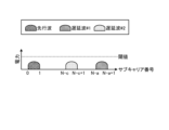
- FIG. 6 is a diagram showing an example of the received signal spectrum after FFT processing of the first signal detection section 216 shown in FIG.
- the delay amounts of the delayed wave #1 and the delayed wave #2 are a chips and b chips, respectively, where the delay amount a is an integral multiple of the chip time rate 1/N, and the delay amount b is the chip time rate 1/N. It shall be a non-integer multiple of .
- the threshold detector 221-1 of the first signal detector 216 detects the preceding wave and the delayed wave #1, which are signals exceeding the threshold, and detects subcarrier number "0" of the detected signal. and “N ⁇ a” and the power of these subcarriers are notified to power peak position detection section 223 .
- FIG. 7 is a diagram showing an example of the received signal spectrum after FFT processing of the second signal detection section 217-i shown in FIG.
- the threshold detection unit 221-i of the second signal detection unit 217-i detects the delayed wave #2 exceeding the threshold, and the subcarrier number “Nc” of the detected signal and the subcarrier power is notified to the power peak position detection unit 223 .
- FIG. 8 is a diagram showing an example of the received signal spectrum after FFT processing of the second signal detection section 217-K shown in FIG.
- the threshold detector 221-K of the second signal detector 217-K notifies the power peak position detector 223 that there is no signal exceeding the threshold because there is no signal exceeding the threshold.
- the number of the signal detection unit which is identification information for specifying the signal detection unit corresponding to the subcarrier number, is notified to the delay amount determination unit 224 .
- the signal detection unit corresponding to the subcarrier number is the signal detection unit that notifies the power peak position detection unit 223 of the subcarrier number, and the first signal detection unit 216 or the second signal detection unit Any one of the parts 217-2 to 217-K.
- the number of the first signal detector 216 is "#1"
- the number of the second signal detectors 217 is "#2 to #K".
- the power peak position detector 223 selects the notified power among the plurality of signal detectors corresponding to the subcarrier numbers.
- the delay amount determination unit 224 is notified of the number specifying the signal detection unit with the largest .
- the delay amount determination unit 224 is notified of “#1”, the subcarrier number “Nc”, and the signal detection unit number “#i”.
- the delay amount determining section 224 estimates the delay amount of each of the plurality of signals included in the received signal based on the information notified from the power peak position detecting section 223, and extracts the delay amount information indicating the estimation result as the pilot signal.
- the unit 211 is notified.
- the method of estimating the delay amount differs between the first signal detection section 216 and the second signal detection section 217 .
- the delay amount determining section 224 sets the delay amount of the subcarrier detected by the first signal detecting section 216 to be "0" when the subcarrier number is "0", and the subcarrier number is "0". Otherwise, it is calculated using the following formula (3).
- the delay amount determination unit 224 calculates the delay amount of the subcarrier detected by the second signal detection unit 217-i using the following formula (4) when the subcarrier number is "0", and determines the subcarrier If the number is other than "0", it is calculated using the following formula (5).
- i is the number of the signal detector and takes a value from 2 to K;
- the subcarrier number “N ⁇ c” is the second 2 signal detection unit 217-i
- the delay amount is ⁇ (N ⁇ c)+N+i/(K+1) chips.
- Each function of transmitter 10 and the receiver 20 is implemented by a processing circuit.
- These processing circuits may be implemented by dedicated hardware, or may be control circuits using a CPU (Central Processing Unit).
- CPU Central Processing Unit
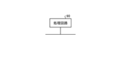
- FIG. 9 is a diagram showing dedicated hardware for implementing the functions of transmitter 10 and receiver 20 according to the first embodiment.
- the processing circuit 90 is a single circuit, a composite circuit, a programmed processor, a parallel programmed processor, an ASIC (Application Specific Integrated Circuit), an FPGA (Field Programmable Gate Array), or a combination thereof.
- ASIC Application Specific Integrated Circuit
- FPGA Field Programmable Gate Array
- FIG. 10 is a diagram showing the configuration of a control circuit 91 for implementing the functions of transmitter 10 and receiver 20 according to the first embodiment.
- the control circuit 91 includes a processor 92 and a memory 93.
- the processor 92 is a CPU, and is also called an arithmetic unit, microprocessor, microcomputer, DSP (Digital Signal Processor), or the like.
- the memory 93 is, for example, non-volatile or volatile semiconductor memory such as RAM (Random Access Memory), ROM (Read Only Memory), flash memory, EPROM (Erasable Programmable ROM), EEPROM (registered trademark) (Electrically EPROM), They include magnetic discs, flexible discs, optical discs, compact discs, mini discs, and DVDs (Digital Versatile Disks).
- the control circuit 91 When the above processing circuit is realized by the control circuit 91, it is realized by the processor 92 reading and executing a program stored in the memory 93 and corresponding to the processing of each component.
- the memory 93 is also used as temporary memory in each process executed by the processor 92 .
- the program executed by the processor 92 may be provided while being stored in a storage medium, or may be provided via a communication channel.
- each function of the transmitter 10 may be realized by different processing circuits for each function of the plurality of blocks shown in FIG.
- the functions of a plurality of blocks may be collectively realized by one processing circuit.
- the receiver 20 and the functions of the plurality of blocks shown in FIGS.
- the functions of a plurality of blocks may be collectively realized by one processing circuit.
- 1 communication system 10 transmitter, 20 receiver, 90 processing circuit, 91 control circuit, 92 processor, 93 memory, 101 modulation section, 102 pilot generation section, 103, 213 spreading section, 104 CP addition section, 105 transmission antenna section , 201 reception antenna unit, 202 synchronization unit, 203 CP removal unit, 204 transmission path estimation unit, 205 equalization unit, 206, 209, 215 despreading unit, 207 demodulation unit, 208 delayed wave estimation unit, 210, 219, 219 -1 to 219-K FFT unit, 211 pilot signal extraction unit, 212 IFFT unit, 214 transmission path estimation processing unit, 216 first signal detection unit, 217, 217-2 to 217-K second signal detection unit, 218 delay amount estimator, 220 noise estimator, 221, 221-1 to 221-K threshold detector, 222, 222-2 to 222-K frequency shifter, 223 power peak position detector, 224 delay amount determiner.
Landscapes
- Engineering & Computer Science (AREA)
- Computer Networks & Wireless Communication (AREA)
- Signal Processing (AREA)
- Power Engineering (AREA)
- Mobile Radio Communication Systems (AREA)
Abstract
Priority Applications (5)
| Application Number | Priority Date | Filing Date | Title |
|---|---|---|---|
| CN202180104351.5A CN118302961A (zh) | 2021-11-26 | 2021-11-26 | 通信装置、通信系统、通信方法、控制电路以及存储介质 |
| DE112021008292.2T DE112021008292B4 (de) | 2021-11-26 | 2021-11-26 | Kommunikationsvorrichtung, kommunikationssystem, kommunikationsverfahren, steuerschaltung und speichermedium |
| JP2023544772A JP7387076B2 (ja) | 2021-11-26 | 2021-11-26 | 通信装置、通信システム、通信方法、制御回路および記憶媒体 |
| PCT/JP2021/043475 WO2023095308A1 (fr) | 2021-11-26 | 2021-11-26 | Dispositif de communication, système de communication, procédé de communication, circuit de commande, et support de stockage |
| US18/644,220 US20240275639A1 (en) | 2021-11-26 | 2024-04-24 | Communication apparatus, communication system, communication method, control circuit, and storage medium |
Applications Claiming Priority (1)
| Application Number | Priority Date | Filing Date | Title |
|---|---|---|---|
| PCT/JP2021/043475 WO2023095308A1 (fr) | 2021-11-26 | 2021-11-26 | Dispositif de communication, système de communication, procédé de communication, circuit de commande, et support de stockage |
Related Child Applications (1)
| Application Number | Title | Priority Date | Filing Date |
|---|---|---|---|
| US18/644,220 Continuation US20240275639A1 (en) | 2021-11-26 | 2024-04-24 | Communication apparatus, communication system, communication method, control circuit, and storage medium |
Publications (1)
| Publication Number | Publication Date |
|---|---|
| WO2023095308A1 true WO2023095308A1 (fr) | 2023-06-01 |
Family
ID=86539208
Family Applications (1)
| Application Number | Title | Priority Date | Filing Date |
|---|---|---|---|
| PCT/JP2021/043475 Ceased WO2023095308A1 (fr) | 2021-11-26 | 2021-11-26 | Dispositif de communication, système de communication, procédé de communication, circuit de commande, et support de stockage |
Country Status (5)
| Country | Link |
|---|---|
| US (1) | US20240275639A1 (fr) |
| JP (1) | JP7387076B2 (fr) |
| CN (1) | CN118302961A (fr) |
| DE (1) | DE112021008292B4 (fr) |
| WO (1) | WO2023095308A1 (fr) |
Families Citing this family (1)
| Publication number | Priority date | Publication date | Assignee | Title |
|---|---|---|---|---|
| CN120111523A (zh) * | 2024-08-16 | 2025-06-06 | 中兴通讯股份有限公司 | 一种通信方法、装置、存储介质及程序产品 |
Citations (4)
| Publication number | Priority date | Publication date | Assignee | Title |
|---|---|---|---|---|
| JP2003069530A (ja) * | 2001-08-24 | 2003-03-07 | Mitsubishi Electric Corp | マルチキャリアcdma受信装置 |
| JP2004297444A (ja) * | 2003-03-27 | 2004-10-21 | Motorola Inc | 制御されたチャネル推定を行なう通信システム |
| JP2008124942A (ja) * | 2006-11-15 | 2008-05-29 | Nec Corp | 無線通信システム、無線通信装置及びそれらに用いる有効パス検出方法 |
| JP2012070131A (ja) * | 2010-09-22 | 2012-04-05 | Nec Casio Mobile Communications Ltd | 通信装置、受信信号処理方法およびプログラム |
Family Cites Families (6)
| Publication number | Priority date | Publication date | Assignee | Title |
|---|---|---|---|---|
| JPS5645613U (fr) | 1979-09-19 | 1981-04-23 | ||
| JP3200547B2 (ja) * | 1995-09-11 | 2001-08-20 | 株式会社日立製作所 | Cdma方式移動通信システム |
| US5999048A (en) * | 1998-01-13 | 1999-12-07 | Lucent Technologies Inc. | Method and apparatus for spread spectrum pilot extraction for RF amplifiers |
| JP4323103B2 (ja) * | 2001-02-20 | 2009-09-02 | 三菱電機株式会社 | 移動体通信システム、マルチキャリアcdma送信装置およびマルチキャリアcdma受信装置 |
| CN100566222C (zh) * | 2001-09-28 | 2009-12-02 | 富士通株式会社 | 信道预测设备和方法 |
| WO2006077620A1 (fr) * | 2005-01-18 | 2006-07-27 | Fujitsu Limited | Méthode de transmission et appareil de transmission dans un système de communication ofdm-cdma |
-
2021
- 2021-11-26 JP JP2023544772A patent/JP7387076B2/ja active Active
- 2021-11-26 WO PCT/JP2021/043475 patent/WO2023095308A1/fr not_active Ceased
- 2021-11-26 CN CN202180104351.5A patent/CN118302961A/zh active Pending
- 2021-11-26 DE DE112021008292.2T patent/DE112021008292B4/de active Active
-
2024
- 2024-04-24 US US18/644,220 patent/US20240275639A1/en active Pending
Patent Citations (4)
| Publication number | Priority date | Publication date | Assignee | Title |
|---|---|---|---|---|
| JP2003069530A (ja) * | 2001-08-24 | 2003-03-07 | Mitsubishi Electric Corp | マルチキャリアcdma受信装置 |
| JP2004297444A (ja) * | 2003-03-27 | 2004-10-21 | Motorola Inc | 制御されたチャネル推定を行なう通信システム |
| JP2008124942A (ja) * | 2006-11-15 | 2008-05-29 | Nec Corp | 無線通信システム、無線通信装置及びそれらに用いる有効パス検出方法 |
| JP2012070131A (ja) * | 2010-09-22 | 2012-04-05 | Nec Casio Mobile Communications Ltd | 通信装置、受信信号処理方法およびプログラム |
Also Published As
| Publication number | Publication date |
|---|---|
| CN118302961A (zh) | 2024-07-05 |
| US20240275639A1 (en) | 2024-08-15 |
| JP7387076B2 (ja) | 2023-11-27 |
| DE112021008292B4 (de) | 2025-09-11 |
| JPWO2023095308A1 (fr) | 2023-06-01 |
| DE112021008292T5 (de) | 2024-07-18 |
Similar Documents
| Publication | Publication Date | Title |
|---|---|---|
| JP4263119B2 (ja) | Ofdmシステムでの初期周波数の同期方法および装置 | |
| US9756657B2 (en) | Wireless network signal to interference plus noise ratio estimation for a random access channel | |
| Gaspar et al. | A synchronization technique for generalized frequency division multiplexing | |
| US20030185179A1 (en) | Radio communication apparatus and radio communication method | |
| US20130034140A1 (en) | Apparatus and method for estimating doppler spread in mobile communication system | |
| EP1988645A1 (fr) | Dispositif et procede d'egalisation | |
| CN101467412A (zh) | 多载波通信系统中的信号检测 | |
| WO2006096728A2 (fr) | Systeme et procede de mesure de distance | |
| EP1848114A2 (fr) | Procédé pour détecter une séquence prédéterminée dans un signal RF utilisant une combinaison de corrélation et de FFT | |
| US9780819B2 (en) | System and method for improving narrowband interference performance | |
| CN102387108A (zh) | 一种物理随机接入信道信号的传输方法及装置 | |
| JP7387076B2 (ja) | 通信装置、通信システム、通信方法、制御回路および記憶媒体 | |
| CA2735007C (fr) | Synchronisation de bases de temps de liaisons radio en « long term evolution » (lte) | |
| KR20080000212A (ko) | 직교주파수분할다중접속 시스템의 레인징 채널 처리 장치및 방법 | |
| US7616723B2 (en) | Method for symbol timing synchronization and apparatus thereof | |
| CN109479035B (zh) | 用于ZT DFT-s-OFDM的信道估计 | |
| RU2414083C2 (ru) | Оценка канала связи | |
| US20110182346A1 (en) | Apparatus and method for estimating noise and interference power in communication system | |
| JP4809445B2 (ja) | 無線品質を測定する装置及び方法 | |
| KR101346436B1 (ko) | Cazac 코드 기반 이동통신 시스템에서 무선 환경적응형 채널 추정 장치 및 방법 | |
| US7860178B2 (en) | Guard section length detection method and system | |
| JP2004304473A (ja) | マルチキャリア受信装置及び回線補償方法 | |
| JP7366329B2 (ja) | 受信装置、通信システム、制御回路および記憶媒体 | |
| JP7378687B2 (ja) | 受信装置、受信同期方法、制御回路、および記憶媒体 | |
| JP7446550B2 (ja) | 受信装置、通信システム、制御回路、記憶媒体および通信方法 |
Legal Events
| Date | Code | Title | Description |
|---|---|---|---|
| 121 | Ep: the epo has been informed by wipo that ep was designated in this application |
Ref document number: 21965678 Country of ref document: EP Kind code of ref document: A1 |
|
| WWE | Wipo information: entry into national phase |
Ref document number: 2023544772 Country of ref document: JP |
|
| WWE | Wipo information: entry into national phase |
Ref document number: 202180104351.5 Country of ref document: CN |
|
| WWE | Wipo information: entry into national phase |
Ref document number: 112021008292 Country of ref document: DE |
|
| 122 | Ep: pct application non-entry in european phase |
Ref document number: 21965678 Country of ref document: EP Kind code of ref document: A1 |
|
| WWG | Wipo information: grant in national office |
Ref document number: 112021008292 Country of ref document: DE |