WO2023095323A1 - Circuit optique, circuit intégré optique et procédé pour fournir une lumière de sortie indépendante de la polarisation - Google Patents
Circuit optique, circuit intégré optique et procédé pour fournir une lumière de sortie indépendante de la polarisation Download PDFInfo
- Publication number
- WO2023095323A1 WO2023095323A1 PCT/JP2021/043593 JP2021043593W WO2023095323A1 WO 2023095323 A1 WO2023095323 A1 WO 2023095323A1 JP 2021043593 W JP2021043593 W JP 2021043593W WO 2023095323 A1 WO2023095323 A1 WO 2023095323A1
- Authority
- WO
- WIPO (PCT)
- Prior art keywords
- optical
- component
- attenuation
- polarization
- optical circuit
- Prior art date
- Legal status (The legal status is an assumption and is not a legal conclusion. Google has not performed a legal analysis and makes no representation as to the accuracy of the status listed.)
- Ceased
Links
Images





Classifications
-
- G—PHYSICS
- G02—OPTICS
- G02B—OPTICAL ELEMENTS, SYSTEMS OR APPARATUS
- G02B6/00—Light guides; Structural details of arrangements comprising light guides and other optical elements, e.g. couplings
- G02B6/10—Light guides; Structural details of arrangements comprising light guides and other optical elements, e.g. couplings of the optical waveguide type
- G02B6/12—Light guides; Structural details of arrangements comprising light guides and other optical elements, e.g. couplings of the optical waveguide type of the integrated circuit kind
-
- G—PHYSICS
- G02—OPTICS
- G02B—OPTICAL ELEMENTS, SYSTEMS OR APPARATUS
- G02B6/00—Light guides; Structural details of arrangements comprising light guides and other optical elements, e.g. couplings
- G02B6/10—Light guides; Structural details of arrangements comprising light guides and other optical elements, e.g. couplings of the optical waveguide type
- G02B6/12—Light guides; Structural details of arrangements comprising light guides and other optical elements, e.g. couplings of the optical waveguide type of the integrated circuit kind
- G02B6/126—Light guides; Structural details of arrangements comprising light guides and other optical elements, e.g. couplings of the optical waveguide type of the integrated circuit kind using polarisation effects
-
- G—PHYSICS
- G02—OPTICS
- G02B—OPTICAL ELEMENTS, SYSTEMS OR APPARATUS
- G02B6/00—Light guides; Structural details of arrangements comprising light guides and other optical elements, e.g. couplings
- G02B6/24—Coupling light guides
- G02B6/26—Optical coupling means
- G02B6/27—Optical coupling means with polarisation selective and adjusting means
- G02B6/2726—Optical coupling means with polarisation selective and adjusting means in or on light guides, e.g. polarisation means assembled in a light guide
-
- G—PHYSICS
- G02—OPTICS
- G02B—OPTICAL ELEMENTS, SYSTEMS OR APPARATUS
- G02B6/00—Light guides; Structural details of arrangements comprising light guides and other optical elements, e.g. couplings
- G02B6/24—Coupling light guides
- G02B6/26—Optical coupling means
- G02B6/28—Optical coupling means having data bus means, i.e. plural waveguides interconnected and providing an inherently bidirectional system by mixing and splitting signals
- G02B6/293—Optical coupling means having data bus means, i.e. plural waveguides interconnected and providing an inherently bidirectional system by mixing and splitting signals with wavelength selective means
- G02B6/29379—Optical coupling means having data bus means, i.e. plural waveguides interconnected and providing an inherently bidirectional system by mixing and splitting signals with wavelength selective means characterised by the function or use of the complete device
- G02B6/2938—Optical coupling means having data bus means, i.e. plural waveguides interconnected and providing an inherently bidirectional system by mixing and splitting signals with wavelength selective means characterised by the function or use of the complete device for multiplexing or demultiplexing, i.e. combining or separating wavelengths, e.g. 1xN, NxM
-
- G—PHYSICS
- G02—OPTICS
- G02B—OPTICAL ELEMENTS, SYSTEMS OR APPARATUS
- G02B6/00—Light guides; Structural details of arrangements comprising light guides and other optical elements, e.g. couplings
- G02B6/24—Coupling light guides
- G02B6/26—Optical coupling means
- G02B6/35—Optical coupling means having switching means
- G02B6/3594—Characterised by additional functional means, e.g. means for variably attenuating or branching or means for switching differently polarized beams
Definitions
- the present invention relates to an optical circuit, an optical integrated circuit and a method for providing polarization independent output light.
- Patent Document 1 "input light whose plane of polarization varies with time is input to orthogonal polarization separation means 12 via variable polarization rotation means 11, and S polarization (vertical polarization) and P polarization (horizontal polarization), two optical paths are combined by the combining means 14, the S-polarized or P-polarized optical path, a polarization rotation means 15 is inserted, and one of the planes of polarization (S polarized wave) is aligned with the other plane of polarization (P-polarized wave), and output as one linear polarized wave (P-polarized wave) from the multiplexing means 14 to the polarization-maintaining optical fiber” (paragraph 0008), “variable polarized wave As the rotating means 11, for example, a Faraday rotator is used. use a wave plate” (Paragraph 0014).
- Patent Literature [Patent Document 1] Japanese Patent Application Laid-Open No. 9-90299
- a first aspect of the present invention provides an optical circuit.
- the optical circuit converts a first polarization direction component of the input light and a second polarization direction component of the input light orthogonal to the first polarization direction into the first polarization direction.
- a polarization rotation separation element that spatially separates and outputs the component may be provided.
- the optical circuit may include a multiplexer that is arranged on the output side of the polarization rotator and multiplexes the first component and the second component.
- the optical circuit is arranged on the output side of the polarization rotator and separates one of the first component and the second component, both the first component and the second component, and the combined light combined by the multiplexer.
- At least one attenuating element may be provided for attenuating the optical power of any of them.
- the at least one attenuating element may attenuate any optical power by an attenuation amount such that the optical power of the combined light output from the optical circuit has a predetermined magnitude.
- At least one attenuating element is disposed between the polarization rotator and the multiplexer, and at least the ratio of the optical power lost in the polarization rotator between the first component and the second component is relatively A small component of the optical power may be attenuated.
- At least one attenuating element has a predetermined proportion of optical power lost between the first component and the second component being input to the polarization rotating/separating element and being input to the multiplexer. Either optical power may be attenuated with an attenuation amount that is equal within the range.
- At least one attenuating element may be arranged between the polarization rotating splitter and the multiplexer, one on each optical path of the first component and the second component.
- the at least one attenuating element has a relative proportion of the optical power lost in the polarization rotation separation element in the respective optical paths of the first component and the second component between the polarization rotation separation element and the multiplexer. It may be placed only on the optical path of the small component.
- the optical circuit is disposed on the optical path between both the multiplexer and the at least one attenuating element and the output side of the optical circuit to direct a portion of the combined light in a direction different from the path to the output side of the optical circuit. It may further include an optical branch coupler for branching into.
- the optical circuit is configured to determine in advance the amount of attenuation of the optical power by the at least one attenuation element so that the optical power of the combined light output from the optical circuit has a predetermined magnitude.
- a light receiving element that receives part of the wave light may be further provided.
- the optical circuit is further arranged on the respective optical paths of the first component and the second component between the polarization rotating splitter and the multiplexer, and transmits a portion of the first component and the second component to the multiplexer.
- a second optical splitting coupler may be provided for splitting in a direction different from the path of .
- the optical circuit further includes a second optical branch coupler for determining in advance the amount of attenuation of the optical power by the at least one attenuating element so that the optical power of the combined light output from the optical circuit has a predetermined magnitude.
- a second light-receiving element may be provided for receiving part of the branched first and second components.
- At least one attenuating element is disposed between the multiplexer and the output side of the optical circuit, and attenuates the combined light by an attenuation amount such that the optical power of the combined light output from the optical circuit has a predetermined magnitude. Power may be attenuated.
- the optical circuit further includes an optical branch coupler arranged on the optical path between the multiplexer and the at least one attenuating element to split a portion of the combined light in a direction different from the path to the at least one attenuating element. You may prepare.
- the optical circuit is further branched by an optical branch coupler in order to adjust the amount of attenuation of the optical power by at least one attenuation element in real time so that the optical power of the combined light output from the optical circuit has a predetermined magnitude.
- a light receiving element for receiving part of the multiplexed light may be provided.
- the optical circuit may further comprise at least one phase shifter for aligning the phases of the first component and the second component between the polarization rotator and the multiplexer.
- a second aspect of the present invention provides an optical integrated circuit.
- the optical integrated circuit may comprise optical functional elements.
- An optical integrated circuit may comprise any of the optical circuits described above.
- the optical circuit may input the output multiplexed light to the optical functional element.
- a third aspect of the present invention provides a method.
- the method converts a first component of input light in a first polarization direction and a component of input light in a second polarization direction orthogonal to the first polarization direction into a first polarization direction by a polarization rotation separation element. and spatially separately outputting the directionally transformed second component.
- the method may comprise combining the first component and the second component with a combiner located at the output of the polarization rotating splitting element.
- the method combines one of the first component and the second component, both the first component and the second component, and a combiner by at least one attenuation element arranged on the output side of the polarization rotating separation element. attenuating the optical power of any of the combined lights.
- the method may comprise adjusting the amount of attenuation of the optical power by the at least one attenuating element such that the optical power of the output combined light has a predetermined magnitude.
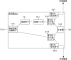
- FIG. 1 is a diagram schematically showing an example of an optical integrated circuit 10 including the optical circuit 100 according to the first embodiment
- FIG. 4 is a flow chart showing an example of an attenuation adjustment method according to the first embodiment
- 5 is a flowchart illustrating an example method for providing polarization independent output light to the optical functional element 50 according to the first embodiment.
- FIG. 4 is a diagram schematically showing an example of an optical circuit 101 according to a second embodiment
- FIG. 11 is a diagram schematically showing an example of an optical circuit 200 according to a third embodiment
- FIG. 10 is a flow chart showing an example of an attenuation adjustment method according to the third embodiment
- FIG. 12 is a diagram schematically showing an example of an optical circuit 201 according to a fourth embodiment
- FIG. 12 is a diagram schematically showing an example of an optical circuit 300 according to a fifth embodiment
- FIG. FIG. 14 is a diagram schematically showing an example of an optical circuit 301 according to a sixth embodiment
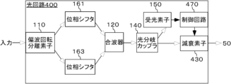
- FIG. 21 is a diagram schematically showing an example of an optical circuit 400 according to a seventh embodiment
- FIG. FIG. 12 is a flowchart illustrating an example method for providing polarization independent output light to an optical functional device 50 according to a seventh embodiment
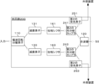
- FIG. 1 is a diagram schematically showing an example of an optical integrated circuit 10 including an optical circuit 100 according to the first embodiment.
- the optical integrated circuit 10 is used for an optical test as an optical waveguide type optical switch, for example, and calibrates the input light input to the optical integrated circuit 10 and outputs the calibrated light.
- the input light is monochromatic and phase-matched coherent light, such as laser light.
- the input light may be polarized or in any polarization state.
- the plane of polarization of the input light may or may not change from moment to moment.
- the amount of light input to the optical integrated circuit 10, that is, the magnitude of the optical power is known.
- the magnitude of the optical power is adjusted in advance on the upstream side of the optical integrated circuit 10 so that the optical power of the input light input to the optical integrated circuit 10 has a predetermined magnitude.
- the optical integrated circuit 10 may have a function of adjusting itself so that the optical power of the input light input to the optical integrated circuit 10 has a predetermined level.
- the optical integrated circuit 10 includes an optical functional element 50 and an optical circuit 100 .
- the optical integrated circuit 10 may be an integrated circuit in which the optical functional element 50 and the optical circuit 100 are integrally mounted on the same substrate.
- the optical functional device 50 may be an optical waveguide type optical device such as a semiconductor laser, an optical modulator, or a photodetector.
- the optical functional element 50 has characteristics that depend on the polarization state of the input light input to the optical functional element 50 .
- the optical circuit 100 is, for example, an optical waveguide type circuit using an optical fiber.
- the optical circuit 100 calibrates the input light that enters the optical circuit 100 in order to provide the optical functional element 50 with polarization-independent output light.
- the optical circuit 100 converts at least the input light into a linearly polarized wave having one polarization direction and outputs the linearly polarized wave.
- the optical circuit 100 separates the input light into a component in one polarization direction and a component obtained by converting a component in another polarization direction orthogonal to the one polarization direction into the one polarization direction. and then combine and output them. Preferably, the optical circuit 100 aligns the phases of the two separated components before combining them.
- the optical circuit 100 inputs the combined light to be output to the optical functional element 50 .
- the optical circuit 100 attenuates the optical power of input light input to the optical circuit 100 and outputs the combined light.
- the optical circuit 100 attenuates the optical power of the input light to the optical power required by the optical functional device 50 .
- the optical circuit 100 includes a polarization rotator 110 , a multiplexer 120 , and attenuation elements 131 and 133 .
- Polarization rotator/separator 110 converts a first component of input light in a first polarization direction and a component of input light in a second polarization direction orthogonal to the first polarization direction into the first polarization direction. spatially separated from the transformed second component and output.
- the first component is, for example, a TE polarized wave (a plane wave in which the electric field is perpendicular to the plane of incidence; orthogonally polarized wave), and the component in the second polarization direction is, for example, a TM polarized wave (a magnetic field perpendicular to the plane of incidence).
- the second component obtained by converting the component in the second polarization direction to the first polarization direction is the TE polarization.
- the first component may be the TM polarized wave and the component in the second polarization direction may be the TE polarized wave.
- the polarization rotator/separator 110 may be, for example, a waveguide connecting optical circuit A, optical circuit B, and optical circuit C in this order, and light is input to optical circuit A and output from optical circuit C. .
- the polarization rotating/separating element 110 has the function of outputting a TE polarized wave without converting it and converting a TM polarized wave into a TE polarized wave and outputting it
- optical circuit A, optical circuit B, and optical circuit C are described below. Each function of is described in detail.
- the optical circuit A has a mode conversion function.
- the optical circuit A outputs the TE fundamental mode as it is with respect to the TE polarized wave input.
- the optical circuit A converts the TM fundamental mode into the TE primary mode by using a waveguide structure that destroys vertical symmetry with respect to the TM polarized wave input, and outputs the converted TE primary mode.
- the optical circuit B functions as an asymmetric directional coupler having two waveguides adjacent to each other, and the light output from the optical circuit A is input to one of the waveguides. With respect to the TE polarized wave input, the optical circuit B outputs the TE fundamental mode input from the optical circuit A as it is in the TE fundamental mode from the output end of the one waveguide.
- the optical circuit B transfers the power of the TE primary mode converted from the TM fundamental mode, which is input from the optical circuit A, to the TE fundamental mode from one waveguide to the other waveguide for the TM polarization input. It is converted into a mode and output from the output end of the other waveguide.
- the optical circuit C has two waveguides whose output ends are spatially separated, and the light output from the two output ends of the optical circuit B is input to the respective input ends of the two waveguides.
- the optical circuit C outputs the TE fundamental mode input from the optical circuit B to the input end of one waveguide as the TE fundamental mode from the output end of the one waveguide.
- the optical circuit C converts the TE fundamental mode converted from the TE primary mode, which is input from the optical circuit B to the input end of the other waveguide, into the other waveguide without changing the TE fundamental mode. output from the output end of
- the multiplexer 120 is arranged on the output side of the polarization rotator 110 and multiplexes the first and second components spatially separated and output by the polarization rotator 110 .
- the attenuation elements 131 and 133 are arranged on the output side of the polarization rotation separation element 110 .
- the attenuating elements 131 and 133 according to the present embodiment are arranged between the polarization rotating/separating element 110 and the multiplexer 120 so that the first component and the second component spatially separated and output by the polarization rotating/separating element 110 are output.
- the attenuation element 131 is arranged on the optical path of the TE polarized wave that is the first component, and the TE polarized wave that is the second component converted from the TM polarized wave that is the component in the second polarization direction is on the optical path of the TE polarized wave.
- Attenuation element 133 is arranged at .
- the attenuating elements 131, 133 may attenuate the optical power of both the first and second components, and only one of the attenuating elements 131, 133 may attenuate the corresponding one of the first and second components. may be attenuated.
- the other of the attenuation elements 131 and 133 is arranged on the optical path of the other of the first component and the second component. may be placed or not.
- the optical circuit 100 may further include an optical branch coupler 140 and a light receiving element 150 .
- the optical branching coupler 140 according to the present embodiment is arranged on the optical path between both the multiplexer 120 and the attenuation elements 131 and 133 and the output side of the optical circuit 100, and the multiplexed light combined by the multiplexer 120 is branched in a direction different from the route to the output side of the optical circuit 100 . The remainder of the multiplexed light multiplexed by the multiplexer 120 travels to the output side of the optical circuit 100 .
- the light receiving element 150 receives the combined light split by the optical splitting coupler 140 out of the combined light multiplexed by the multiplexer 120 .
- the purpose of the light receiving element 150 according to the present embodiment is to determine in advance the amount of attenuation of the optical power by the attenuating elements 131 and 133 so that the optical power of the combined light output from the optical circuit 100 has a predetermined magnitude. , is provided in the optical circuit 100 together with the optical branch coupler 140 .
- the multiplexer located downstream of the light receiving element etc. 120 and the waveguide may cause optical insertion loss, in which case the light receiving element cannot accurately detect the optical power of the output light provided to the optical functional element 50 .
- the light-receiving element 150 according to the present embodiment is arranged along with the optical branching coupler 140 on the optical path between both the multiplexer 120 and attenuation elements 131 and 133 and the output side of the optical circuit 100 .
- the light-receiving element 150 is arranged on the optical path on the upstream side of at least one of the multiplexer 120 and the attenuating elements 131 and 133 as described above.
- the optical power of the output light provided to 50 can be detected more accurately.
- the optical branching coupler 140 and the light receiving element 150 may be removed from the optical path of the optical circuit 100 as soon as the amount of attenuation by the attenuation elements 131 and 133 is determined.
- the signal indicating the magnitude of the optical power detected by the light receiving element 150 may be sent to an external device such as a personal computer for the above purpose.
- the user uses the personal computer to determine the amount of attenuation of the optical power by the attenuating elements 131 and 133 so that the optical power of the multiplexed light output from the optical circuit 100 has a predetermined magnitude. good too.
- the optical circuit 100 may be provided with optical power detection means other than the light receiving element 150 instead of the light receiving element 150 .
- the optical circuit 100 may further include phase shifters 161 and 163 .
- Phase shifters 161 and 163 align the phases of the first component and the second component between polarization rotator 110 and multiplexer 120 .
- the phase shifters 161, 163 may align the phases of the first and second components with each other by delaying the phase of both the first and second components by a predetermined amount.
- phase shifters 161 and 163 delays the phase of the corresponding one of the first component and the second component by a predetermined amount, so that the phases of the first component and the second component are shifted. may be aligned with each other.
- the other of the phase shifters 161 and 163 is arranged on the optical path of the other of the first and second components. It may or may not be placed.
- the predetermined amount of phase delay described above may be determined in consideration of the characteristics of the polarization rotator 110, for example.
- phase shifters 161 and 163 may be heaters.
- the optical circuit 100 adjusts the length of the optical paths in which the attenuation elements 131 and 133 are arranged, respectively, so that the phases of the first component and the second component are shifted to each other. You can arrange them.
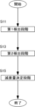
- FIG. 2 is a flowchart showing an example of an attenuation adjustment method according to the first embodiment.
- the optical circuit 100 according to this embodiment executes the attenuation adjustment method shown in FIG.
- the optical circuit 100 executes the first detection stage (step S11). Specifically, in the optical circuit 100, only the TE polarized wave having a known optical power is input to the optical circuit 100 with the attenuation amounts of the attenuation elements 131 and 133 set to 0%. to detect The optical circuit 100 transmits a signal indicating the magnitude of the optical power detected by the light receiving element 150 to an external device.
- the input light containing only the TE polarized wave and not the TM polarized wave travels along the optical path where the attenuation element 131 is arranged without being converted by the polarization rotation separation element 110, and the attenuation element 133 is arranged. Do not proceed along the optical path.
- the optical circuit 100 executes the second detection stage (step S13). Specifically, in the optical circuit 100, only the TM polarized wave having the same optical power as that in the first detection stage is input to the optical circuit 100 with the attenuation of the attenuation elements 131 and 133 set to 0%. Optical power is detected at 150 . The optical circuit 100 transmits a signal indicating the magnitude of the optical power detected by the light receiving element 150 to an external device. The input light containing only the TM polarized wave and not containing the TE polarized wave is converted to the TE polarized wave by the polarization rotation separating element 110 and travels along the optical path in which the attenuation element 133 is arranged, and the attenuation element 131 is arranged. do not follow the designated light path.
- the optical circuit 100 executes the attenuation adjustment stage based on the detection results of the first detection stage and the second detection stage (step S15). Specifically, the optical circuit 100 determines the amount of attenuation of the optical power by the attenuation elements 131 and 133 so that the optical power of the multiplexed light output from the optical circuit 100 has a predetermined magnitude.
- the predetermined amount of optical power is the optical power required by the optical functional device 50, for example.
- the optical circuit 100 can generate the combined light output from the optical circuit 100 regardless of the ratio of the first component in the first polarization direction and the component in the second polarization direction orthogonal to the first polarization direction in the input light. can be made constant.
- the attenuation elements 131 and 133 have, as an example, a configuration in which the user can adjust the amount of attenuation for attenuating the optical power.
- the attenuation amount may be the ratio of the attenuated optical power to the optical power of the input light expressed as a percentage, and may be set within a range of 0 to 100%.
- the attenuation elements 131 and 133 may be selected from a plurality of attenuation elements set to different attenuation amounts.
- the attenuation elements 131 and 133 whose attenuation amounts are determined as described above, provide an attenuation amount at which the optical power of the multiplexed light output from the optical circuit 100 has a predetermined magnitude.
- One optical power is attenuated.
- Attenuating elements 131 and 133 attenuate the optical power of at least the component of the first component and the second component that has a relatively small ratio of the optical power lost in polarization rotator/separator 110 .
- a component with a relatively small ratio of optical power lost by the polarization rotating/separating element 110 is a second component converted from the second polarization direction to the first polarization direction by the polarization rotating/separating element 110, for example, from the TE polarized wave. Transformed TM polarization.
- the attenuating elements 131 and 133 are the first and second components of the light that is lost between the input to the polarization rotator/separator 110 and the input to the multiplexer 120. Attenuate the optical power of both or one of the first component and the second component by an attenuation amount in which the proportion of the power is equal to each other within a predetermined range.
- the optical circuit 100 equalizes the insertion loss ratios of the first component and the second component that occur in the optical circuit 100 .
- the TE polarized wave having a known optical power loses 10% of the optical power due to passing through the polarization rotation separation element 110
- the optical power required by the optical functional element 50 is assumed to be 70% of the known optical power.
- the optical circuit 100 may determine the attenuation of the attenuation element 131 to be 20% and the attenuation of the attenuation element 133 to be 10%.
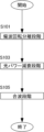
- FIG. 3 is a flowchart illustrating an example of a method for providing polarization-independent output light to the optical functional device 50 according to the first embodiment.
- the optical circuit 100 according to the present embodiment executes the attenuation adjustment method shown in the flowchart of FIG. 2 before executing the method shown in the flowchart of FIG. is adjusted to a predetermined magnitude.
- the optical circuit 100 performs the polarization rotation separation stage (step S101). Specifically, the optical circuit 100 uses the polarization rotation splitting element 110 to convert the first component of the input light in the first polarization direction and the second component of the input light in the first polarization direction orthogonal to the first polarization direction. A second component obtained by converting the polarization direction component into the first polarization direction is spatially separated and output.
- the optical circuit 100 performs an optical power attenuation step (step S103). Specifically, the optical circuit 100 attenuates the optical power of one or both of the first component and the second component by the attenuation elements 131 and 133 arranged on the output side of the polarization rotator/separator 110 .
- the optical circuit 100 executes the multiplexing stage (step S105). Specifically, the optical circuit 100 multiplexes the first component and the second component by the multiplexer 120 arranged on the output side of the polarization rotator/separator 110 . As a result, the optical circuit 100 outputs, for example, a TE polarized wave as output light that does not depend on polarization, and inputs the TE polarized wave to the optical functional device 50 .
- the optical circuit 100 align the phases of the first and second components by the phase shifters 161 and 163 after performing the optical power attenuation stage and before performing the multiplexing stage.
- the first component which is the component of the input light in the first polarization direction
- the component of the input light which is in the second polarization direction orthogonal to the first polarization direction
- a multiplexer 120 for multiplexing.
- the optical circuit 100 further comprises at least one attenuation element 131, 133 arranged at the output side of the polarization rotator 110 for attenuating the optical power of one or both of the first and second components.
- the light intensity of the S-polarized wave and the P-polarized wave of the input light is adjusted by the Faraday rotator, the two polarized waves are separated by the polarization beam splitter, and then the S-polarized wave is generated by the half-wave plate. is rotated to form a P-polarized wave, and an optical circuit is assumed that combines and outputs two P-polarized waves.
- the optical circuit according to the comparative example further includes a beam splitter and a photodetector set on each optical path of the two separated polarized waves in order to adjust the light intensity of the S polarized wave and the P polarized wave of the input light in real time. , and feeds back data indicating the light intensity detected by the photodetector to the polarization control circuit.
- the optical circuit 100 of the present embodiment having the above configuration, one or both of the first component and the second component in the same polarization direction, which are output from the polarization rotator/separator 110
- the power is attenuated by at least one attenuation element 131 , 133 arranged at the output side of the polarization rotating separation element 110 .
- the optical circuit 100 according to the present embodiment does not require elements such as a Faraday rotator, a polarization beam splitter and a half-wave plate, and waveguides connecting these elements, compared to the optical circuit according to the comparative example.
- the optical circuit 100 according to the present embodiment can be made smaller than the optical circuit according to the comparative example, thereby contributing to the miniaturization of the optical integrated circuit 10 on which the optical circuit 100 is mounted. can be done.
- a combination of one polarization rotator 110 and at least one attenuation element 131, 133 can be realized with a size of 100 ⁇ m ⁇ 800 ⁇ m or less.
- the polarization state of the input light is adjusted by adjusting the amount of attenuation of the optical power by the attenuation elements 131 and 133 so that the optical power of the output multiplexed light has a predetermined magnitude.
- Polarization-independent output light can be provided for the optical functional device 50 having characteristics that depend on .
- FIG. 4 is a diagram schematically showing an example of the optical circuit 101 according to the second embodiment.
- the optical circuit 101 according to the present embodiment differs from the optical circuit 100 according to the first embodiment in that it does not include the set of the attenuation element 133 and the phase shifter 163 but only the set of the attenuation element 131 and the phase shifter 161 .
- Other configurations in the optical circuit 101 are the same as the corresponding configurations in the optical circuit 100, so the same reference numerals are used to omit redundant description.
- the same reference numbers as those in the optical circuit 100 are used to overlap. Description is omitted. The same applies to a plurality of embodiments described below.
- the attenuator 131 is located between the polarization rotator 110 and the multiplexer 120 in the respective optical paths of the first component and the second component. It is placed only on the optical path of the component for which the percentage of optical power lost at 110 is relatively small.
- the second component is the optical power loss when the component in the second polarization direction is converted by the polarization rotation separation element 110. is relatively large. Therefore, the optical circuit 101 additionally attenuates the optical power of the first component so that the optical power becomes the same as the optical power of the relatively large lost second component.
- the attenuation element 131 attenuates the optical power of only the component, of the first component and the second component, which has a relatively small proportion of the optical power lost in the polarization rotator/separator 110 .
- phase shifter 161 is arranged only on the optical path where the attenuation element 131 is arranged.
- phase shifters 161 and 163 may be arranged on their respective optical paths, with only phase shifter 163 being arranged only on optical paths where attenuation element 131 is not arranged.
- the optical circuit 101 according to the second embodiment described above also has the same effects as those of the optical circuit 100 according to the first embodiment.
- FIG. 5 is a diagram schematically showing an example of the optical circuit 200 according to the third embodiment.
- the optical circuit 200 according to the present embodiment differs from the optical circuit 100 according to the first embodiment in that, instead of the optical branching coupler 140 and the light receiving element 150, second optical branching couplers 241 and 243 and a second light receiving element 251 are provided. , 253 .
- the second optical branch couplers 241 and 243 are arranged on the respective optical paths of the first component and the second component, between the polarization rotator/separator 110 and the multiplexer 120. A part is branched in a direction different from the path to the multiplexer 120 . More specifically, the second optical branch couplers 241 and 243 are arranged between the phase shifters 161 and 163 and the multiplexer 120 on the respective optical paths of the first and second components.
- the second light receiving elements 251 and 253 receive part of the first and second components split by the second optical split couplers 241 and 243 .
- the second light receiving elements 251 and 253 are, like the light receiving element 150 in the first embodiment, the attenuation elements 131 and 133 so that the optical power of the multiplexed light output from the optical circuit 200 has a predetermined magnitude. It is provided in the optical circuit 200 together with the second optical branch couplers 241 and 243 for the purpose of predetermining the amount of attenuation of the optical power.
- the light-receiving element is arranged along with the optical splitting coupler on the optical path of only one of the first component and the second component, the optical power of the other of the first component and the second component can be detected. Therefore, the above objective cannot be achieved. Further, when the light receiving element is arranged on the optical path of the first component and the second component on the upstream side of the phase shifters 161 and 163 together with the optical branch coupler, the phase shifters 161 and 163 located on the downstream side of the light receiving element and the like are arranged. In this case, the light-receiving element cannot accurately detect the optical power of the output light provided to the optical functional element 50 .
- the second light receiving elements 251 and 253 according to the present embodiment, together with the second optical branch couplers 241 and 243, between the phase shifters 161 and 163 and the multiplexer 120, the first component and the second component are arranged on respective optical paths of Thereby, the second light receiving elements 251 and 253 can avoid any of the above problems.
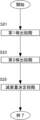
- FIG. 6 is a flowchart showing an example of an attenuation adjustment method according to the third embodiment.
- the optical circuit 200 according to the present embodiment performs the attenuation adjustment method shown in FIG. Execute.
- the optical circuit 200 performs the first detection stage (step S21). Specifically, the optical circuit 200 inputs only the TE polarized wave having a known optical power into the optical circuit 200 with the attenuation amounts of the attenuation elements 131 and 133 set to 0%. to detect the optical power. The optical circuit 200 transmits a signal indicating the magnitude of the optical power detected by the second light receiving element 251 to an external device. The input light containing only the TE polarized wave and not the TM polarized wave travels along the optical path where the attenuation element 131 is arranged without being converted by the polarization rotation separation element 110, and the attenuation element 133 is arranged. Do not proceed along the optical path.
- the optical circuit 200 performs the second detection stage (step S23). Specifically, the optical circuit 200 inputs only the TM polarized wave having the same optical power as that of the first detection stage to the optical circuit 200 with the attenuation of the attenuation elements 131 and 133 set to 0%, and the second detection stage The optical power is detected by the light receiving element 253 of . The optical circuit 200 transmits a signal indicating the magnitude of the optical power detected by the second light receiving element 253 to an external device.
- the input light containing only the TM polarized wave and not containing the TE polarized wave is converted to the TE polarized wave by the polarization rotation separating element 110 and travels along the optical path in which the attenuation element 133 is arranged, and the attenuation element 131 is arranged. do not follow the designated light path.
- the optical circuit 200 executes the attenuation adjustment stage based on the detection results of the first detection stage and the second detection stage (step S25). Since step S25 is the same as step S15 shown in the flowchart of FIG. 2, redundant description will be omitted.
- the optical circuit 200 according to the third embodiment described above also has the same effect as the optical circuit 100 according to the first embodiment.
- FIG. 7 is a diagram schematically showing an example of the optical circuit 201 according to the fourth embodiment.
- the optical circuit 201 according to the present embodiment differs from the optical circuit 200 according to the third embodiment in that it does not include the set of the attenuation element 133 and the phase shifter 163 but only the set of the attenuation element 131 and the phase shifter 161 .
- the attenuation element 131 is arranged between the polarization rotation separation element 110 and the multiplexer 120 to Among the respective optical paths, it is arranged only on the optical path of the component in which the proportion of the optical power lost in the polarization rotator/separator 110 is relatively small. That is, the optical circuit 201 additionally attenuates the optical power of the first component so that the optical power becomes the same as the optical power of the relatively large lost second component.
- the attenuation element 131 attenuates the optical power of only the component, of the first component and the second component, which has a relatively small proportion of the optical power lost in the polarization rotator/separator 110 .
- phase shifter 161 is arranged only on the optical path where the attenuation element 131 is arranged.
- phase shifters 161 and 163 may be arranged in their respective optical paths, with only phase shifter 163 being arranged only in optical paths where attenuation element 131 is not arranged.
- the optical circuit 201 according to the fourth embodiment described above also has the same effects as those of the optical circuit 100 according to the first embodiment.
- FIG. 8 is a diagram schematically showing an example of the optical circuit 300 according to the fifth embodiment.
- the optical circuit 300 according to the present embodiment differs from the optical circuit 100 according to the first embodiment in that, in addition to the configuration of the optical circuit 100, second optical branch couplers 241 and 243 and second light receiving elements 251 and 253 are added. Prepare.
- the optical circuit 300 according to the present embodiment has a configuration in which the configuration included in the optical circuit 100 according to the first embodiment and the configuration included in the optical circuit 200 according to the third embodiment are combined.
- the optical circuit 300 performs the method for providing polarization-independent output light to the optical functional device 50 shown in the flowchart in FIG.
- the adjustment method may be performed, the attenuation amount adjustment method shown in the flowchart of FIG. 6 may be performed, and these two attenuation amount adjustment methods may be performed simultaneously or sequentially.
- the optical circuit 300 according to the fourth embodiment described above also has the same effect as the optical circuit 100 according to the first embodiment.
- FIG. 9 is a diagram schematically showing an example of the optical circuit 301 according to the sixth embodiment.
- the optical circuit 301 according to the present embodiment differs from the optical circuit 300 according to the fifth embodiment in that it does not include the set of the attenuation element 133 and the phase shifter 163 but only the set of the attenuation element 131 and the phase shifter 161 .
- the attenuation element 131 causes the first component and the second component to Among the respective optical paths, it is arranged only on the optical path of the component in which the proportion of the optical power lost in the polarization rotator/separator 110 is relatively small. That is, the optical circuit 301 additionally attenuates the optical power of the first component so that the optical power becomes the same as the optical power of the relatively large lost second component.
- the attenuation element 131 attenuates the optical power of only the component, of the first component and the second component, which has a relatively small proportion of the optical power lost in the polarization rotator/separator 110 .
- phase shifter 161 is arranged only on the optical path where the attenuation element 131 is arranged.
- phase shifters 161 and 163 may be arranged on their respective optical paths, with only phase shifter 163 being arranged only on optical paths where attenuation element 131 is not arranged.
- the optical circuit 301 does not have to include the second optical branch coupler 243 and the second light receiving element 253 in the configuration shown in FIG.
- the optical circuit 301 without the second optical splitting coupler 243 and the second light receiving element 253 uses the method for providing polarization-independent output light to the optical functional element 50 shown in the flow chart of FIG. may be executed as a step prior to executing the attenuation amount adjustment method shown in the flowchart of FIG. You may perform the attenuation amount adjustment method which consists of.
- the optical circuit 301 inputs only the TE polarized wave having a known optical power into the optical circuit 301 with the attenuation amounts of the attenuation elements 131 and 133 set to 0% to receive the second light.
- Optical power is detected by element 251 .
- the optical circuit 301 inputs only the TM polarized wave having the same optical power as this, and the light receiving element 150 detects the optical power.
- the optical circuit 301 executes the above step S25 based on these detection results.
- the optical circuit 301 may include the second optical branch coupler 243 and the second light receiving element 253, but may not include the second optical branch coupler 241 and the second light receiving element 251.
- the optical circuit 301 inputs only the TE polarized wave having a known optical power into the optical circuit 301 while the attenuation amounts of the attenuation elements 131 and 133 are set to 0%.
- Optical power is detected by the light receiving element 150 .
- the optical circuit 301 inputs only the TM polarized wave having the same optical power as this, and the second light receiving element 253 detects the optical power.
- the optical circuit 301 executes the above step S25 based on these detection results.
- the optical circuit 301 according to the sixth embodiment also provides the same effects as those of the optical circuit 100 according to the first embodiment.
- FIG. 10 is a diagram schematically showing an example of the optical circuit 400 according to the seventh embodiment.
- the optical circuit 300 according to this embodiment differs from the optical circuit 100 according to the first embodiment in that it does not include the attenuation elements 131 and 133 but includes an attenuation element 430 and a control circuit 470 .
- the attenuation element 430 attenuates the optical power of the multiplexed light multiplexed by the multiplexer 120 . More specifically, the attenuation element 430 is arranged between the multiplexer 120 and the output side of the optical circuit 400, and the optical power of the multiplexed light output from the optical circuit 400 becomes a predetermined magnitude. The optical power of the multiplexed light is attenuated by the attenuation amount.
- the control circuit 470 controls the amount of attenuation by the attenuation element 430 in real time based on the magnitude of the optical power detected by the light receiving element 150 via the optical splitter coupler 140 .
- the optical splitter coupler 140 is arranged on the optical path between the multiplexer 120 and the attenuation element 430, and directs part of the multiplexed light to the attenuation element 430. branch in different directions.
- the light receiving element 150 receives the combined light split by the optical splitting coupler 140 out of the combined light multiplexed by the multiplexer 120 .
- the light-receiving element 150 is intended to adjust the amount of attenuation of the optical power by the attenuation element 430 in real time so that the optical power of the combined light output from the optical circuit 100 has a predetermined magnitude. , are provided in the optical circuit 400 together with the optical branch coupler 140 .
- the optical splitting coupler 140 and the light receiving element 150 are required for the optical circuit 400 to implement a method for providing polarization independent output light to the optical functional element 50 .
- FIG. 11 is a flow chart showing an example of a method for providing polarization-independent output light to the optical functional element 50 according to the seventh embodiment.
- the optical circuit 400 performs a polarization rotation separation step (step S201). Specifically, the optical circuit 400 converts the first component of the input light in the first polarization direction and the second component of the input light orthogonal to the first polarization direction by the polarization rotation splitter 110 . A second component obtained by converting the polarization direction component into the first polarization direction is spatially separated and output.
- the optical circuit 400 performs the multiplexing stage (step S203). Specifically, the optical circuit 400 multiplexes the first component and the second component by the multiplexer 120 arranged on the output side of the polarization rotator 110 . It is preferable that the optical circuit 400 aligns the phases of the first component and the second component by the phase shifters 161 and 163 after executing the polarization rotation splitting stage and before executing the multiplexing stage.
- the optical circuit 400 executes the attenuation adjustment stage (step S205). Specifically, the optical circuit 400 adjusts the amount of attenuation of the optical power by the attenuation element 430 so that the optical power of the output multiplexed light has a predetermined magnitude. More specifically, the control circuit 470 of the optical circuit 400 controls the light of the combined light output from the optical circuit 100 based on the magnitude of the optical power detected by the light receiving element 150 via the optical branching coupler 140. The amount of attenuation of the optical power by the attenuation element 430 is adjusted in real time so that the power becomes a predetermined magnitude.
- the optical circuit 400 performs an optical power attenuation step (step S207). Specifically, the optical circuit 400 attenuates the optical power of the multiplexed light multiplexed by the multiplexer 120 by the attenuation element 430 arranged on the output side of the polarization rotator/separator 110 . As a result, the optical circuit 400 outputs, for example, a TE polarized wave as polarization-independent output light, and inputs the TE polarized wave to the optical functional device 50 .
- the optical circuit 400 according to the seventh embodiment also provides the same effects as the optical circuit 100 according to the first embodiment.
- Optical Integrated Circuit 50 Optical Functional Elements 100, 101, 200, 201, 300, 301, 400 Optical Circuit 110 Polarization Rotation Separation Element 120 Multiplexer 131, 133, 430 Attenuation Element 140 Optical Branch Coupler 150 Light Receiving Elements 161, 163 phase shifters 241, 243 second optical branch couplers 251, 253 second light receiving element 470 control circuit
Landscapes
- Physics & Mathematics (AREA)
- General Physics & Mathematics (AREA)
- Optics & Photonics (AREA)
- Engineering & Computer Science (AREA)
- Microelectronics & Electronic Packaging (AREA)
- Optical Communication System (AREA)
- Optical Integrated Circuits (AREA)
- Polarising Elements (AREA)
Abstract
L'invention concerne un circuit optique (100) comprenant : un élément de séparation/rotation de polarisation (110) qui sépare spatialement et délivre en sortie un premier composant qui est un composant dans une première direction de polarisation à l'extérieur de la lumière d'entrée, et un second composant obtenu par conversion d'un composant dans une seconde direction de polarisation orthogonale à la première direction de polarisation hors de la lumière d'entrée dans la première direction de polarisation ; un multiplexeur (120) qui est disposé sur le côté de sortie de l'élément de rotation/séparation de polarisation (110) et multiplexe le premier composant et le second composant ; et au moins un élément d'atténuation (131, 133) qui est disposé sur le côté de sortie de l'élément de rotation/séparation de polarisation (110) et atténue la puissance optique de l'un du premier composant et du second composant, à la fois du premier composant et du second composant, ou de la lumière multiplexée multiplexée par le multiplexeur (120).
Priority Applications (4)
| Application Number | Priority Date | Filing Date | Title |
|---|---|---|---|
| PCT/JP2021/043593 WO2023095323A1 (fr) | 2021-11-29 | 2021-11-29 | Circuit optique, circuit intégré optique et procédé pour fournir une lumière de sortie indépendante de la polarisation |
| JP2023563471A JP7603845B2 (ja) | 2021-11-29 | 2021-11-29 | 偏波に依存しない出力光を提供するための光回路、光集積回路および方法 |
| TW111142932A TWI843283B (zh) | 2021-11-29 | 2022-11-10 | 用於提供無關於偏振的輸出光的光電路、光積體電路及方法 |
| US18/442,106 US20240219640A1 (en) | 2021-11-29 | 2024-02-15 | Optical circuit, optical integrated circuit, and method for providing polarization-independent output light |
Applications Claiming Priority (1)
| Application Number | Priority Date | Filing Date | Title |
|---|---|---|---|
| PCT/JP2021/043593 WO2023095323A1 (fr) | 2021-11-29 | 2021-11-29 | Circuit optique, circuit intégré optique et procédé pour fournir une lumière de sortie indépendante de la polarisation |
Related Child Applications (1)
| Application Number | Title | Priority Date | Filing Date |
|---|---|---|---|
| US18/442,106 Continuation US20240219640A1 (en) | 2021-11-29 | 2024-02-15 | Optical circuit, optical integrated circuit, and method for providing polarization-independent output light |
Publications (1)
| Publication Number | Publication Date |
|---|---|
| WO2023095323A1 true WO2023095323A1 (fr) | 2023-06-01 |
Family
ID=86539003
Family Applications (1)
| Application Number | Title | Priority Date | Filing Date |
|---|---|---|---|
| PCT/JP2021/043593 Ceased WO2023095323A1 (fr) | 2021-11-29 | 2021-11-29 | Circuit optique, circuit intégré optique et procédé pour fournir une lumière de sortie indépendante de la polarisation |
Country Status (4)
| Country | Link |
|---|---|
| US (1) | US20240219640A1 (fr) |
| JP (1) | JP7603845B2 (fr) |
| TW (1) | TWI843283B (fr) |
| WO (1) | WO2023095323A1 (fr) |
Citations (8)
| Publication number | Priority date | Publication date | Assignee | Title |
|---|---|---|---|---|
| JPH08184788A (ja) * | 1995-01-04 | 1996-07-16 | Canon Inc | 偏光制御装置 |
| JP2007003708A (ja) * | 2005-06-22 | 2007-01-11 | Ricoh Co Ltd | 光集積回路 |
| JP2010060656A (ja) * | 2008-09-01 | 2010-03-18 | Fujitsu Ltd | 偏光状態安定化方法及び装置、光信号処理システム |
| JP2011064657A (ja) * | 2009-09-18 | 2011-03-31 | Nippon Telegr & Teleph Corp <Ntt> | 光回路 |
| WO2016005418A1 (fr) * | 2014-07-08 | 2016-01-14 | Universiteit Gent | Traitement indépendant de polarisation dans la photonique intégrée |
| JP2016535302A (ja) * | 2014-05-23 | 2016-11-10 | 華為技術有限公司Huawei Technologies Co.,Ltd. | 偏光制御デバイスおよび偏光制御方法 |
| US20200319409A1 (en) * | 2019-04-08 | 2020-10-08 | Analog Photonics LLC | Wavelength Division Multiplexing Filter for Multiplexing or Demultiplexing Using Cascaded Frequency Shaping |
| JP2021124578A (ja) * | 2020-02-04 | 2021-08-30 | 富士通株式会社 | 光回路素子、これを用いた光送受信器、及び光回路素子の製造方法 |
Family Cites Families (2)
| Publication number | Priority date | Publication date | Assignee | Title |
|---|---|---|---|---|
| JP7103042B2 (ja) * | 2018-08-03 | 2022-07-20 | 富士通オプティカルコンポーネンツ株式会社 | 光デバイス、光送受信モジュール、および光デバイスの製造方法 |
| US10754091B1 (en) * | 2019-03-18 | 2020-08-25 | Inphi Corporation | Integrated coherent optical transceiver, light engine |
-
2021
- 2021-11-29 WO PCT/JP2021/043593 patent/WO2023095323A1/fr not_active Ceased
- 2021-11-29 JP JP2023563471A patent/JP7603845B2/ja active Active
-
2022
- 2022-11-10 TW TW111142932A patent/TWI843283B/zh active
-
2024
- 2024-02-15 US US18/442,106 patent/US20240219640A1/en active Pending
Patent Citations (8)
| Publication number | Priority date | Publication date | Assignee | Title |
|---|---|---|---|---|
| JPH08184788A (ja) * | 1995-01-04 | 1996-07-16 | Canon Inc | 偏光制御装置 |
| JP2007003708A (ja) * | 2005-06-22 | 2007-01-11 | Ricoh Co Ltd | 光集積回路 |
| JP2010060656A (ja) * | 2008-09-01 | 2010-03-18 | Fujitsu Ltd | 偏光状態安定化方法及び装置、光信号処理システム |
| JP2011064657A (ja) * | 2009-09-18 | 2011-03-31 | Nippon Telegr & Teleph Corp <Ntt> | 光回路 |
| JP2016535302A (ja) * | 2014-05-23 | 2016-11-10 | 華為技術有限公司Huawei Technologies Co.,Ltd. | 偏光制御デバイスおよび偏光制御方法 |
| WO2016005418A1 (fr) * | 2014-07-08 | 2016-01-14 | Universiteit Gent | Traitement indépendant de polarisation dans la photonique intégrée |
| US20200319409A1 (en) * | 2019-04-08 | 2020-10-08 | Analog Photonics LLC | Wavelength Division Multiplexing Filter for Multiplexing or Demultiplexing Using Cascaded Frequency Shaping |
| JP2021124578A (ja) * | 2020-02-04 | 2021-08-30 | 富士通株式会社 | 光回路素子、これを用いた光送受信器、及び光回路素子の製造方法 |
Also Published As
| Publication number | Publication date |
|---|---|
| JPWO2023095323A1 (fr) | 2023-06-01 |
| US20240219640A1 (en) | 2024-07-04 |
| TWI843283B (zh) | 2024-05-21 |
| JP7603845B2 (ja) | 2024-12-20 |
| TW202321751A (zh) | 2023-06-01 |
Similar Documents
| Publication | Publication Date | Title |
|---|---|---|
| US9851615B2 (en) | Optical modulator | |
| US20030174936A1 (en) | Optical wavelength division multiplexer | |
| US20130258453A1 (en) | Quantum entangled photon pair generator | |
| US20100245837A1 (en) | Polarization interferometer, optical module, and optical receiver | |
| JP2018516488A (ja) | 空間分割多重化システム用偏光不感セルフホモダイン検出受信機 | |
| US9835800B2 (en) | Polarization control for a photonic platform | |
| EP2856253A2 (fr) | Commutateur optique de grande puissance | |
| JP6969849B2 (ja) | 偏波制御器を内蔵するスイッチマトリクス | |
| JP7603845B2 (ja) | 偏波に依存しない出力光を提供するための光回路、光集積回路および方法 | |
| CN109791302B (zh) | 光耦合装置及其控制方法 | |
| CN114365033B (zh) | Iq光调制器 | |
| JPH05323243A (ja) | 偏波制御器 | |
| CA2848178C (fr) | Dispositif de commande de polarisation a selection de longueur d'onde | |
| US20100302637A1 (en) | Polarization insensitive optical circuit | |
| JP4820854B2 (ja) | 光受信器 | |
| JP3502578B2 (ja) | 導波路型偏波状態測定器 | |
| CN114779489A (zh) | 一种基于偏振分束结构的全光快速扰偏器 | |
| JP2015513702A (ja) | 先進型の変調フォーマットのための柔軟な光変調器 | |
| JP2002350798A (ja) | 偏波補正器及びこれを用いた波長分割多重装置 | |
| JPH09281537A (ja) | 偏光制御回路 | |
| JP2017142301A (ja) | 厳密固有モード合分波器、及び厳密固有モード多重伝送システム | |
| TWI846445B (zh) | 光回路及方法 | |
| JP2014048411A (ja) | 光信号処理装置 | |
| US20170329084A1 (en) | Polarization dependent loss control for polarization diverse circuit | |
| JP2011146786A (ja) | 位相制御装置 |
Legal Events
| Date | Code | Title | Description |
|---|---|---|---|
| 121 | Ep: the epo has been informed by wipo that ep was designated in this application |
Ref document number: 21965692 Country of ref document: EP Kind code of ref document: A1 |
|
| WWE | Wipo information: entry into national phase |
Ref document number: 2023563471 Country of ref document: JP |
|
| NENP | Non-entry into the national phase |
Ref country code: DE |
|
| 122 | Ep: pct application non-entry in european phase |
Ref document number: 21965692 Country of ref document: EP Kind code of ref document: A1 |