WO2023112814A1 - Dispositif de détection - Google Patents
Dispositif de détection Download PDFInfo
- Publication number
- WO2023112814A1 WO2023112814A1 PCT/JP2022/045233 JP2022045233W WO2023112814A1 WO 2023112814 A1 WO2023112814 A1 WO 2023112814A1 JP 2022045233 W JP2022045233 W JP 2022045233W WO 2023112814 A1 WO2023112814 A1 WO 2023112814A1
- Authority
- WO
- WIPO (PCT)
- Prior art keywords
- light
- photodiode
- organic semiconductor
- semiconductor layer
- detection
- Prior art date
- Legal status (The legal status is an assumption and is not a legal conclusion. Google has not performed a legal analysis and makes no representation as to the accuracy of the status listed.)
- Ceased
Links
Images





Classifications
-
- G—PHYSICS
- G01—MEASURING; TESTING
- G01J—MEASUREMENT OF INTENSITY, VELOCITY, SPECTRAL CONTENT, POLARISATION, PHASE OR PULSE CHARACTERISTICS OF INFRARED, VISIBLE OR ULTRAVIOLET LIGHT; COLORIMETRY; RADIATION PYROMETRY
- G01J1/00—Photometry, e.g. photographic exposure meter
- G01J1/42—Photometry, e.g. photographic exposure meter using electric radiation detectors
- G01J1/44—Electric circuits
-
- G—PHYSICS
- G06—COMPUTING OR CALCULATING; COUNTING
- G06T—IMAGE DATA PROCESSING OR GENERATION, IN GENERAL
- G06T1/00—General purpose image data processing
-
- H—ELECTRICITY
- H10—SEMICONDUCTOR DEVICES; ELECTRIC SOLID-STATE DEVICES NOT OTHERWISE PROVIDED FOR
- H10F—INORGANIC SEMICONDUCTOR DEVICES SENSITIVE TO INFRARED RADIATION, LIGHT, ELECTROMAGNETIC RADIATION OF SHORTER WAVELENGTH OR CORPUSCULAR RADIATION
- H10F30/00—Individual radiation-sensitive semiconductor devices in which radiation controls the flow of current through the devices, e.g. photodetectors
- H10F30/20—Individual radiation-sensitive semiconductor devices in which radiation controls the flow of current through the devices, e.g. photodetectors the devices having potential barriers, e.g. phototransistors
-
- H—ELECTRICITY
- H10—SEMICONDUCTOR DEVICES; ELECTRIC SOLID-STATE DEVICES NOT OTHERWISE PROVIDED FOR
- H10F—INORGANIC SEMICONDUCTOR DEVICES SENSITIVE TO INFRARED RADIATION, LIGHT, ELECTROMAGNETIC RADIATION OF SHORTER WAVELENGTH OR CORPUSCULAR RADIATION
- H10F39/00—Integrated devices, or assemblies of multiple devices, comprising at least one element covered by group H10F30/00, e.g. radiation detectors comprising photodiode arrays
- H10F39/10—Integrated devices
- H10F39/12—Image sensors
-
- H—ELECTRICITY
- H10—SEMICONDUCTOR DEVICES; ELECTRIC SOLID-STATE DEVICES NOT OTHERWISE PROVIDED FOR
- H10K—ORGANIC ELECTRIC SOLID-STATE DEVICES
- H10K39/00—Integrated devices, or assemblies of multiple devices, comprising at least one organic radiation-sensitive element covered by group H10K30/00
- H10K39/30—Devices controlled by radiation
- H10K39/32—Organic image sensors
-
- G—PHYSICS
- G01—MEASURING; TESTING
- G01J—MEASUREMENT OF INTENSITY, VELOCITY, SPECTRAL CONTENT, POLARISATION, PHASE OR PULSE CHARACTERISTICS OF INFRARED, VISIBLE OR ULTRAVIOLET LIGHT; COLORIMETRY; RADIATION PYROMETRY
- G01J1/00—Photometry, e.g. photographic exposure meter
- G01J1/42—Photometry, e.g. photographic exposure meter using electric radiation detectors
- G01J1/44—Electric circuits
- G01J2001/4446—Type of detector
- G01J2001/446—Photodiode
Definitions
- the present invention relates to a detection device.
- an OPD Organic Photodiode
- Patent Document 1 An OPD (Organic Photodiode) using an organic semiconductor material is known (for example, Patent Document 1).
- An object of the present invention is to provide a detection device that uses OPDs and has good detection sensitivity for different wavelengths.
- a detection device of one embodiment of the present invention includes a first detection circuit including a first photodiode sensitive to a first light and a second photodiode sensitive to a second light, and a third photodiode sensitive to a third light.
- a second detection circuit including a photodiode, wherein the first photodiode and the second photodiode constitute a first detection element connected in series and in opposite directions;
- One end side of the detection element is connected to a first signal line via a first transistor, the other end side of the first detection element is supplied with a first drive signal, and the cathode of the third photodiode is:
- a second drive signal is supplied to the anode of the third photodiode, which is connected to the second signal line via the second transistor.
- FIG. 1 is a plan view showing the detection device according to the first embodiment.
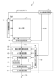
- FIG. 2 is a block diagram showing a configuration example of the detection device according to the first embodiment.
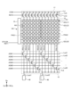
- FIG. 3 is a circuit diagram showing the detection device.
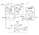
- FIG. 4 is a circuit diagram showing one pixel and detection circuit.
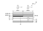
- FIG. 5 is a cross-sectional view schematically showing a cross-section of the detection device according to the first embodiment.
- FIG. 6 is a circuit diagram showing one pixel and detection circuit of the detection device according to the second embodiment.
- FIG. 7 is a circuit diagram showing one pixel and detection circuit of the detection device according to the third embodiment.
- FIG. 8 is a cross-sectional view schematically showing a cross-section of the detection device according to the fourth embodiment.
- FIG. 9 is a cross-sectional view schematically showing a cross-section of the detection device according to the fifth embodiment.
- FIG. 10 is a cross-sectional view schematically showing a cross-section of the detection device according to the sixth embodiment.
- FIG. 11 is a cross-sectional view schematically showing a cross-section of the detection device according to the seventh embodiment.
- FIG. 12 is a diagram showing an example of an electronic device to which the detection device is applied.
- FIG. 1 is a plan view showing the detection device according to the first embodiment.
- the detection device 1 of this embodiment has an OPD (Organic Photodiode) as an optical sensor, and is employed in a color scanner, a digital camera, or the like that captures an image of an object to be detected.
- the detection device 1 includes a substrate 21, a sensor section 10, a gate line drive circuit 15, a signal line selection circuit 16, a detection circuit 48, a control circuit 122, a power supply circuit 123, It has a first light source substrate 51 , a second light source substrate 52 , a first light source 53 , and a second light source 54 .
- a plurality of first light sources 53 are provided on the first light source substrate 51 .
- a plurality of second light sources 54 are provided on the second light source substrate 52 .
- a control board 121 is electrically connected to the board 21 via a wiring board 71 .
- the wiring board 71 is, for example, a flexible printed board or a rigid board.
- a detection circuit 48 is provided on the wiring board 71 .
- a control circuit 122 and a power supply circuit 123 are provided on the control board 121 .
- the control circuit 122 is, for example, an FPGA (Field Programmable Gate Array).
- the control circuit 122 supplies control signals to the sensor section 10 , the gate line drive circuit 15 and the signal line selection circuit 16 to control the detection operation of the sensor section 10 .
- the control circuit 122 also supplies control signals to the first light source 53 and the second light source 54 to control lighting or non-lighting of the first light source 53 and the second light source 54 .
- the power supply circuit 123 supplies voltage signals such as the sensor power supply signal VDDSNS (see FIG. 4) to the sensor section 10, the gate line drive circuit 15, and the signal line selection circuit 16. FIG. Also, the power supply circuit 123 supplies a power supply voltage to the first light source 53 and the second light source 54 .
- the substrate 21 has a detection area AA and a peripheral area GA.
- the detection area AA is an area in which a plurality of photodiodes PD (see FIG. 4) of the sensor section 10 are provided.
- the peripheral area GA is an area between the outer circumference of the detection area AA and the outer edge of the substrate 21, and is an area in which the plurality of photodiodes PD are not provided.
- the gate line drive circuit 15 and the signal line selection circuit 16 are provided in the peripheral area GA. Specifically, the gate line driving circuit 15 is provided in a region extending along the second direction Dy in the peripheral region GA.
- the signal line selection circuit 16 is provided in an area extending along the first direction Dx in the peripheral area GA, and is provided between the sensor section 10 and the detection circuit 48 .
- the first direction Dx is one direction within a plane parallel to the substrate 21 .
- the second direction Dy is one direction in a plane parallel to the substrate 21 and perpendicular to the first direction Dx. Note that the second direction Dy may cross the first direction Dx instead of being perpendicular to it.
- plane view refers to the positional relationship when viewed from a direction perpendicular to the substrate 21 .
- the plurality of first light sources 53 are provided on the first light source substrate 51 and arranged along the second direction Dy.
- a plurality of second light sources 54 are provided on the second light source substrate 52 and arranged along the second direction Dy.
- the first light source base material 51 and the second light source base material 52 are electrically connected to a control circuit 122 and a power supply circuit 123 via terminal portions 124 and 125 provided on the control board 121, respectively.
- the plurality of first light sources 53 and the plurality of second light sources 54 for example, inorganic LEDs (Light Emitting Diodes) or organic ELs (OLEDs: Organic Light Emitting Diodes) are used.
- the plurality of first light sources 53 and the plurality of second light sources 54 each have a plurality of LEDs that emit red (R), green (G), and blue (B) lights.
- the plurality of first light sources 53 and the plurality of second light sources 54 may have a plurality of LEDs that emit white light.
- the light emitted from the first light source 53 and the second light source 54 is reflected by the surface of the object to be detected and enters the sensor section 10 . Thereby, the sensor unit 10 can image the object to be detected.
- the first light source 53 and the second light source 54 may be omitted.
- FIG. 2 is a block diagram showing a configuration example of the detection device according to the first embodiment.
- the detection device 1 further has a detection control circuit 11 and a detection section 40 .
- a part or all of the functions of the detection control circuit 11 are included in the control circuit 122 .
- part or all of the functions of the detection unit 40 other than the detection circuit 48 are included in the control circuit 122 .
- the sensor unit 10 has a plurality of photodiodes PD.
- the photodiode PD included in the sensor unit 10 outputs an electrical signal corresponding to the irradiated light to the signal line selection circuit 16 as the output signal Vdet. Further, the sensor section 10 performs detection according to the gate drive signal Vgcl supplied from the gate line drive circuit 15 .
- the detection control circuit 11 is a circuit that supplies control signals to the gate line drive circuit 15, the signal line selection circuit 16, and the detection section 40, respectively, and controls their operations.
- the detection control circuit 11 supplies the gate line drive circuit 15 with various control signals such as a start signal STV, a clock signal CK, and a reset signal RST1.
- the detection control circuit 11 also supplies various control signals such as the selection signal ASW to the signal line selection circuit 16 . Further, the detection control circuit 11 supplies various control signals to the first light source 53 and the second light source 54 to control lighting and non-lighting of each.
- the gate line drive circuit 15 is a circuit that drives a plurality of gate lines GCL (see FIG. 3) based on various control signals.
- the gate line driving circuit 15 sequentially or simultaneously selects a plurality of gate lines GCL and supplies a gate driving signal Vgcl to the selected gate lines GCL. Thereby, the gate line drive circuit 15 selects a plurality of photodiodes PD connected to the gate line GCL.
- the signal line selection circuit 16 is a switch circuit that sequentially or simultaneously selects a plurality of signal lines SGL (see FIG. 3).
- the signal line selection circuit 16 is, for example, a multiplexer.
- the signal line selection circuit 16 connects the selected signal line SGL and the detection circuit 48 based on the selection signal ASW supplied from the detection control circuit 11 . Thereby, the signal line selection circuit 16 outputs the output signal Vdet of the photodiode PD to the detection section 40 .
- the detection unit 40 includes a detection circuit 48 , a signal processing circuit 44 , a storage circuit 46 , a detection timing control circuit 47 , an image processing circuit 49 and an output processing circuit 50 .
- the detection timing control circuit 47 controls the detection circuit 48, the signal processing circuit 44, and the image processing circuit 49 to operate synchronously based on the control signal supplied from the detection control circuit 11.
- the detection circuit 48 is, for example, an analog front end circuit (AFE, Analog Front End).
- the detection circuit 48 is a signal processing circuit having at least the functions of the detection signal amplification circuit 42 and the A/D conversion circuit 43 .
- the detection signal amplifier circuit 42 amplifies the output signal Vdet.
- the A/D conversion circuit 43 converts the analog signal output from the detection signal amplification circuit 42 into a digital signal.
- the detection circuit 48 outputs red (R), green (G), and blue (B) color signals for each pixel PX.
- the signal processing circuit 44 performs a predetermined correction on the color signals for each of red (R), green (G), and blue (B) received from the detection circuit 48 .
- the signal processing circuit 44 controls the intensity of the light emitted from the first light source 53 and the second light source 54 within the detection area AA and the variation in the detection sensitivity of the photodiode PD.
- a predetermined correction is performed for Further, the signal processing circuit 44 may acquire output signals Vdet simultaneously detected by a plurality of photodiodes PD and perform processing of averaging them.
- the detection unit 40 suppresses measurement errors caused by noise and relative positional deviation between the object to be detected and the sensor unit 10, thereby enabling stable detection.
- the storage circuit 46 temporarily stores the signal calculated by the signal processing circuit 44 .
- the storage circuit 46 may be, for example, a RAM (Random Access Memory), a register circuit, or the like.
- the image processing circuit 49 combines the output signals Vdet output from the photodiodes PD of the sensor unit 10 to generate two-dimensional information of the image.
- the image processing circuit 49 may output the output signal Vdet as the sensor output voltage Vo without calculating the image data. Also, the image processing circuit 49 may not be included in the detection unit 40 .
- the output processing circuit 50 functions as a processing unit that performs processing based on outputs from the multiple photodiodes PD.
- the output processing circuit 50 may include the two-dimensional information generated by the image processing circuit 49 in the sensor output voltage Vo. Also, the function of the output processing circuit 50 may be integrated into another configuration (for example, the image processing circuit 49, etc.).
- FIG. 3 is a circuit diagram showing the detection device.
- the sensor section 10 has a plurality of pixels PX arranged in a matrix.
- a photodiode PD is provided in each of the plurality of pixels PX.
- a plurality of pixels PX including photodiodes PD are arranged on the substrate 21 .
- the photodiode PD is an OPD (Organic Photodiode) using an organic semiconductor.
- OPD Organic Photodiode
- a gate line GCL extends in the first direction Dx and is connected to a plurality of pixels PX arranged in the first direction Dx.
- the signal line SGL extends in the second direction Dy and is connected to the photodiodes PD of the pixels PX arranged in the second direction Dy.
- the sensor section 10 is provided between the signal line selection circuit 16 and the reset circuit 17 .
- the signal line selection circuit 16 and the reset circuit 17 may be connected to the ends of the signal line SGL in the same direction.
- the gate line drive circuit 15 receives various control signals such as the start signal STV, the clock signal CK, and the reset signal RST1 from the control circuit 122 (see FIG. 1).
- the gate line drive circuit 15 sequentially selects a plurality of gate lines GCL(1), GCL(2), .
- the gate line drive circuit 15 supplies a gate drive signal Vgcl to the selected gate line GCL.
- the gate drive signal Vgcl is supplied to the plurality of transistors Tr (the first transistor Tr1 and the second transistor Tr2 (see FIG. 4)) connected to the gate line GCL, and the plurality of pixels arranged in the first direction Dx. PX is selected for detection.
- the signal line selection circuit 16 has multiple selection signal lines Lsel, multiple output signal lines Lout, and a third transistor TrS.
- the multiple third transistors TrS are provided corresponding to the multiple signal lines SGL, respectively.
- Six signal lines SGL(1), SGL(2), . . . , SGL(6) are connected to a common output signal line Lout1.
- Six signal lines SGL(7), SGL(8), . . . , SGL(12) are connected to a common output signal line Lout2.
- the output signal lines Lout1 and Lout2 are connected to the detection circuit 48, respectively.
- the signal lines SGL(1), SGL(2), . Signal line block A plurality of select signal lines Lsel are connected to the gates of the third transistors TrS included in one signal line block. Also, one selection signal line Lsel is connected to the gates of the third transistors TrS of the plurality of signal line blocks.
- the control circuit 122 (see FIG. 1) sequentially supplies the selection signal ASW to the selection signal line Lsel.
- the signal line selection circuit 16 sequentially selects the signal lines SGL in one signal line block in a time division manner by the operation of the third transistor TrS. Also, the signal line selection circuit 16 selects one signal line SGL in each of the plurality of signal line blocks.
- the detection device 1 can reduce the number of ICs (Integrated Circuits) including the detection circuit 48 or the number of IC terminals.
- the signal line selection circuit 16 may bundle a plurality of signal lines SGL and connect them to the detection circuit 48 .
- the reset circuit 17 has a reference signal line Lvr, a reset signal line Lrst and a fourth transistor TrR.
- the fourth transistor TrR is provided corresponding to the plurality of signal lines SGL.
- the reference signal line Lvr is connected to one of the sources or drains of the plurality of fourth transistors TrR.
- the reset signal line Lrst is connected to gates of the plurality of fourth transistors TrR.
- the control circuit 122 supplies the reset signal RST2 to the reset signal line Lrst.
- the multiple fourth transistors TrR are turned on, and the multiple signal lines SGL are electrically connected to the reference signal line Lvr.
- the power supply circuit 123 supplies the reference potential COM to the reference signal line Lvr.
- the reference potential COM is supplied to the capacitive elements Ca1 and Ca2 (see FIG. 4) included in the plurality of pixels PX.
- FIG. 4 is a circuit diagram showing one pixel and a detection circuit. Note that FIG. 4 also shows the circuit configuration of the power supply circuit 123 .
- the pixel PX includes a first detection circuit SPX1 and a second detection circuit SPX2.
- the first detection circuit SPX1 and the second detection circuit SPX2 have sensitivities to light in different wavelength regions. Specifically, the first detection circuit SPX1 detects first light, which is red (R) light, and second light, which is green (G) light, among the light incident on the pixel PX.
- the second detection circuit SPX2 detects third light, which is blue (B) light.
- the first detection circuit SPX1 includes a first photodiode PD-R sensitive to the first light, a second photodiode PD-G sensitive to the second light, a capacitive element Ca1, and a first transistor Tr1.
- the first photodiode PD-R and the second photodiode PD-G are connected in series and in opposite directions (first detection element). Note that "connected in the opposite direction” indicates a connection configuration in which the rectification characteristics of the first photodiode PD-R and the second photodiode PD-G are in the opposite direction.
- the anode of the first photodiode PD-R and the anode of the second photodiode PD-G are electrically connected.
- One end side of the first photodiode PD-R and the second photodiode PD-G connected in series, that is, the cathode of the first photodiode PD-R is connected to the first signal line SGL ( n).
- the other end side of the first photodiode PD-R and the second photodiode PD-G connected in series, that is, the cathode of the second photodiode PD-G is electrically connected to the drive signal supply circuit 123a (power supply circuit 123). , and supplied with a drive signal VDDSNS (first drive signal).
- the capacitive elements Ca1 and Ca2 are capacitances (sensor capacitances) formed in the photodiode PD and equivalently connected in parallel with the photodiode PD.
- one end side of the capacitive element Ca1 is electrically connected to the cathode of the first photodiode PD-R, and the other end side of the capacitive element Ca1 is connected to the cathode of the second photodiode PD-G. electrically connected.
- the first transistor Tr1 is provided corresponding to the photodiode PD (the first photodiode PD-R and the second photodiode PD-G).
- the first transistor Tr1 is composed of a thin film transistor, and in this example, is composed of an n-channel MOS (Metal Oxide Semiconductor) type TFT (Thin Film Transistor).
- the gate of the first transistor Tr1 is connected to the gate line GCL (see FIG. 3).
- the source of the first transistor Tr1 is connected to the first signal line SGL(n).
- the drain of the first transistor Tr1 is connected to the cathode of the first photodiode PD-R and one end side of the capacitive element Ca1.
- the second detection circuit SPX2 includes a third photodiode PD-B sensitive to the third light, a capacitive element Ca2, and a second transistor Tr2.
- the second detection circuit SPX2 is configured with one third photodiode PD-B, unlike the first detection circuit SPX1.
- the cathode of the third photodiode PD-B is connected to the second signal line SGL(n+1) through the second transistor Tr2.
- the anode of the third photodiode PD-B is electrically connected to the drive signal supply circuit 123a (power supply circuit 123) and supplied with the drive signal VDDSNS (second drive signal).
- first photodiode PD-R when there is no need to distinguish between the first photodiode PD-R, the second photodiode PD-G, and the third photodiode PD-B, they may simply be referred to as photodiodes PD. be. Further, when the first signal line SGL(n) and the second signal line SGL(n+1) need not be distinguished and described, they may simply be referred to as the signal line SGL.
- one end side of the capacitive element Ca2 is electrically connected to the cathode of the third photodiode PD-B, and the other end side of the capacitive element Ca2 is connected to the anode of the third photodiode PD-B. electrically connected.
- the second transistor Tr2 is provided corresponding to the third photodiode PD-B.
- the second transistor Tr2 is composed of a thin film transistor like the first transistor Tr1.
- the gate of the second transistor Tr2 is connected to the gate line GCL (see FIG. 3).
- the source of the second transistor Tr2 is connected to the second signal line SGL(n+1).
- the drain of the second transistor Tr2 is connected to the cathode of the third photodiode PD-B and one end side of the capacitive element Ca2.
- Signal lines SGL and respective A reference potential COM (see FIG. 3) is supplied as the initial potential of the photodiode PD.
- a bias voltage VB is supplied to each photodiode PD by the drive signal VDDSNS and the reference potential COM.
- the drive signal supply circuit 123a that supplies the drive signal VDDSNS to each photodiode PD of the first detection circuit SPX1 and the second detection circuit SPX2 includes a first voltage signal supply circuit 123H, a second voltage signal supply circuit 123L, and a switch BSW. and
- the first voltage signal supply circuit 123H is a circuit that supplies a first voltage signal VH having a higher level voltage than the reference potential COM.
- the second voltage signal supply circuit 123L is a circuit that supplies a second voltage signal VL having a lower level voltage than the reference potential COM.
- the switch BSW is a switch element that switches connection states between the first voltage signal supply circuit 123H and the second voltage signal supply circuit 123L and the photodiodes PD of the first detection circuit SPX1 and the second detection circuit SPX2.
- the drive signal supply circuit 123a supplies the first voltage signal VH and the second voltage signal VL in a time division manner to the photodiodes PD of the first detection circuit SPX1 and the second detection circuit SPX2.
- the second photodiode PD-G is forward-biased, the second transistor Tr2 is gated off, or the third transistor TrS connected to the path is turned off. It is desirable to make the path of .
- the first detection circuit SPX1 when the drive signal supply circuit 123a supplies the first voltage signal VH (VH>COM) to the cathode of the second photodiode PD-G, the first photodiode PD -R is forward bias driven and the second photodiode PD-G is reverse bias driven.
- the second photodiode PD-G detects the second light (G), and forward current flows through the first photodiode PD-R.
- the “refresh operation” represents an operation of returning the characteristics of the OPD to its initial state by passing a forward bias current through the photodiode PD.
- the first photodiode PD-R when the second voltage signal VL (VL ⁇ COM) is supplied from the drive signal supply circuit 123a to the cathode of the second photodiode PD-G, the first photodiode PD-R is reverse bias driven, Photodiode PD-G is forward bias driven. In this case, the first photodiode PD-R detects the first light (R), a forward current flows through the second photodiode PD-G, and refresh is performed.
- VL VL ⁇ COM
- the second detection circuit SPX2 when the first voltage signal VH (VH>COM) is supplied from the drive signal supply circuit 123a to the anode of the third photodiode PD-B, for example, the second transistor Tr2 is gated off, 3 Photodiode PD-B is not forward-biased and refreshed. Further, when the second voltage signal VL (VL ⁇ COM) is supplied from the drive signal supply circuit 123a to the anode of the third photodiode PD-B, the third photodiode PD-B is reverse bias driven and 3 light (B) is detected.
- VL VL ⁇ COM
- the detection device 1 detects the first light (R) by the first photodiode PD-R and the detection of the second light (G) by the second photodiode PD-G in the first detection circuit SPX1. Do it in parts. Further, the detection device 1 may detect the third light (B) by the third photodiode PD-B in the second detection circuit SPX2 in synchronization with the detection by the first detection circuit SPX1. The detection may be performed in a time-sharing manner without synchronizing with the detection of the 1 detection circuit SPX1.
- the drive signal VDDSNS (first drive signal) supplied to the first detection circuit SPX1 and the drive signal VDDSNS (second drive signal) supplied to the second detection circuit SPX2 are synchronous signals having the same potential. , or different signals may be supplied to each.
- the second photodiode PD-G is forward-biased, the second transistor Tr2 is gated off, or the third transistor TrS connected to the path is turned off. It is desirable to make the path of .
- the photodiodes PD (the first photodiode PD-R, the second photodiode PD-G, and the third photodiode PD-B) are exposed to the A current corresponding to the light amount of the first light, the second light, and the third light flows, thereby accumulating charges in the capacitive element Ca1.
- the first transistor Tr1 or the second transistor Tr2 is turned on, current flows through the signal line SGL according to the charge accumulated in the capacitive element Ca1.
- the signal line SGL is electrically connected to the detection circuit 48 via the third transistor TrS of the signal line selection circuit 16 .
- the detection device 1 can detect a signal corresponding to the amount of light irradiated to each photodiode PD for each pixel PX.
- the detection circuit 48 is connected to the signal line SGL with the switch SSW turned on during the readout period.
- the detection signal amplifier circuit 42 of the detection circuit 48 converts the current fluctuation supplied from the signal line SGL into a voltage fluctuation and amplifies it.
- a reference potential (Vref) having a fixed potential is input to the non-inverting input (+) of the detection signal amplifier circuit 42, and the signal line SGL is connected to the inverting input (-).
- the same signal as the reference potential COM is input as the reference potential (Vref) voltage.
- the signal processing circuit 44 calculates the difference between the output signal Vdet when light is irradiated and the output signal Vdet when light is not irradiated as the sensor output voltage Vo.
- the detection signal amplifier circuit 42 has a capacitive element Cb and a reset switch RSW. During the reset period, the reset switch RSW is turned on to reset the charge of the capacitive element Cb.
- FIG. 5 is a cross-sectional view schematically showing a cross-section of the detection device according to the first embodiment.
- the first photodiode PD-R, the second photodiode PD-G, and the third photodiode PD-B are provided on the first main surface S1 of the substrate .
- the detection device 1 according to the first embodiment is a top light-receiving optical sensor, and the light L1 is incident from the first main surface S1 side of the substrate 21 .
- the substrate 21 is an insulating base material, for example, glass or resin material is used.
- the substrate 21 is a flat member having a first principal surface S1 and a second principal surface S2 opposite to the first principal surface S1.
- the substrate 21 is not limited to a flat plate shape, and may have a curved surface. In this case, the substrate 21 may be a film-like resin.
- the first photodiode PD-R includes a first organic semiconductor layer 31 sensitive to the first light.
- the second photodiode PD-G includes a second organic semiconductor layer 32 sensitive to the second light.
- a second organic semiconductor layer 32 (second photodiode PD-G), a first organic semiconductor layer 31 (first photodiode PD-R ) are stacked in this order. However, the stacking order of the second organic semiconductor layer 32 (second photodiode PD-G) and the first organic semiconductor layer 31 (first photodiode PD-R) may be reversed.
- the third photodiode PD-B includes a laminated structure in which the first organic semiconductor layer 31 and the second organic semiconductor layer 32 are laminated.
- the second organic semiconductor layer 32, the first organic semiconductor layer 31, and the wavelength conversion layer 81 are laminated in this order on the first main surface S1 of the substrate 21 in the region overlapping the second detection circuit SPX2.
- the wavelength conversion layer 81 is laminated on the incident surface side of the light L1 (the upper surface of the first organic semiconductor layer 31 in FIG. 5) of the second organic semiconductor layer 32 and the first organic semiconductor layer 31 .
- the second detection circuit SPX2 includes the third photodiode PD-B and the wavelength conversion layer 81 that converts the third light into the first light or the second light.
- the first organic semiconductor layer 31 and the second organic semiconductor layer 32 are continuously provided from the region overlapping the first detection circuit SPX1 to the region overlapping the second detection circuit SPX2. That is, the first organic semiconductor layer 31 forming the first photodiode PD-R and the first organic semiconductor layer 31 forming the third photodiode PD-B are continuously formed in the same layer.
- the second organic semiconductor layer 32 forming the photodiode PD-G and the second organic semiconductor layer 32 forming the third photodiode PD-B are continuously formed in the same layer.
- the wavelength conversion layer 81 For the wavelength conversion layer 81, a wavelength conversion film, a wavelength cut film that cuts a specific wavelength component and transmits other wavelength components, or the like can be used.
- the wavelength conversion layer 81 converts the third light (B) component of the light L1 into the first light (R).
- the first photodiode PD-R of the first detection circuit SPX1 outputs the output signal Vdet(R) based on the first light (R) of the light L1.
- the second light (G) component of the light L1 is not absorbed by the first organic semiconductor layer 31 (first photodiode PD-R) and enters the second organic semiconductor layer 32 (second photodiode PD-G). do.
- the second photodiode PD-G of the first detection circuit SPX1 outputs an output signal Vdet(G) based on the second light (G) of the light L1.
- the first organic semiconductor layer 31 (third photodiode PD-B) of the second detection circuit SPX2 converts the light L1 from the third light (B) into the first light (R) by the wavelength conversion layer 81. It outputs an output signal Vdet(B) based on the light.
- the signal processing circuit 44 (see FIG. 3) performs arithmetic processing of each output signal Vdet from the first photodiode PD-R, the second photodiode PD-G, and the third photodiode PD-B as necessary.
- the output signal Vdet (B) of the first detection circuit SPX1 is converted from the output value of the output signal Vdet (B) from the third photodiode PD-B.
- R can be subtracted to obtain the detection value of the second detection circuit SPX2.
- the detection device 1 detects the first light (R) and the second light (G) with the first photodiode PD-R, the second photodiode PD-G, and the third photodiode PD-B, respectively. , the third light (B) can be detected.
- the first photodiode PD-R and the second photodiode PD-G are formed of the first organic semiconductor layer 31 and the second organic semiconductor layer 32 laminated on the substrate 21, and are formed into one first detection circuit. Configured as SPX1.
- one first detection circuit SPX1 has sensitivity to each of the first light (R) and the second light (G).
- the second detection circuit SPX2 has sensitivity to the third light (B).
- detection elements with three different sensitivities of RGB were required to detect a color image.
- the SPX2 can detect the first light (R), the second light (G) and the third light (B).
- FIG. 6 is a circuit diagram showing one pixel and detection circuit of the detection device according to the second embodiment.
- the same reference numerals are assigned to the same components as those described in the above-described embodiment, and overlapping descriptions will be omitted.
- the second detection circuit SPX2 has a third photodiode PD-B and a fourth photodiode PD-A.
- the fourth photodiode PD-A is sensitive to light other than the first light (R), the second light (G) and the third light (B) (for example, near-infrared light).
- the third photodiode PD-B and the fourth photodiode PD-A are connected in series and in opposite directions.
- the connection configuration between the third photodiode PD-B and the fourth photodiode PD-A is the same as that of the first detection circuit SPX1 described above, and repeated description will be omitted.
- the wavelength conversion layer 81 has, for example, the function of converting the third light (B) component of the light L1 into the first light (R), in addition to the near-infrared component into the second light (G).
- the second organic semiconductor layer 32 of the second detection circuit SPX2 shown in FIG. 5 functions as the fourth photodiode PD-A and can detect near-infrared components. That is, the second organic semiconductor layer 32 forming the second photodiode PD-G and the second organic semiconductor layer 32 forming the fourth photodiode PD-A are continuously formed in the same layer.
- FIG. 7 is a circuit diagram showing one pixel and detection circuit of the detection device according to the third embodiment.
- the pixel PX includes a first photodiode PD-R, a second photodiode PD-G, two capacitive elements Ca1 and Ca2, and a second photodiode PD-G. 1 transistor Tr1 and 2nd transistor Tr2 are included.
- the cathode of the first photodiode PD-R is connected to the first signal line SGL(n) through the first transistor Tr1 and to the second signal line SGL(n+1) through the second transistor Tr2. be.
- the drive signal VDDSNS is supplied from the drive signal supply circuit 123a to the cathode of the second photodiode PD-G.
- one of the first photodiode PD-R and the second photodiode PD-G also functions as the third photodiode PD-B.
- the first photodiode PD-R detects the first light (R)
- the second photodiode PD-G detects the second light ( G) is detected.
- the first transistor Tr1 is off and the second transistor Tr2 is on
- one of the first photodiode PD-R and the second photodiode PD-G detects the third light (B).
- the number of photodiodes PD included in one pixel PX can be reduced compared to the above-described embodiments. Also, with such a configuration, the conventional protocol can be used as it is.
- FIG. 8 is a cross-sectional view schematically showing a cross-section of the detection device according to the fourth embodiment.
- the detection device 1C according to the fourth embodiment further has a light shielding layer 82 and a reflective layer 83.
- the detection device 1C according to the fourth embodiment is a bottom-surface-receiving type optical sensor, and the light L1 is incident from the second main surface S2 side of the substrate 21 .
- the light shielding layer 82, the wavelength conversion layer 81, and the reflection layer 83 are formed on the surface of the first organic semiconductor layer 31 and the second organic semiconductor layer 32 opposite to the incident surface of the light L1 (first surface in FIG. 8). provided on the upper surface of the organic semiconductor layer 31).
- the second organic semiconductor layer 32 and the first organic semiconductor layer 31 are laminated on the first main surface S1 of the substrate 21 in this order.
- the stacking order of the second organic semiconductor layer 32 and the first organic semiconductor layer 31 may be reversed.
- a wavelength conversion layer 81 and a reflection layer 83 are provided in this order on the upper surface of the first organic semiconductor layer 31 (the surface opposite to the incident surface of the light L1).
- the wavelength conversion layer 81 and the reflection layer 83 are continuously provided over the first detection circuit SPX1 and the second detection circuit SPX2.
- the light shielding layer 82 is provided between the first organic semiconductor layer 31 and the wavelength conversion layer 81 in a region overlapping with the first detection circuit SPX1. Also, the light shielding layer 82 is not provided in a region overlapping with the second detection circuit SPX2.
- the second organic semiconductor layer 32 (second photodiode PD-G) and the first organic semiconductor layer 31 (first photodiode PD-G) are formed on the first main surface S1 of the substrate 21 in the region overlapping the first detection circuit SPX1.
- PD-R a light shielding layer 82, a wavelength conversion layer 81, and a reflective layer 83 are laminated in this order.
- a second organic semiconductor layer 32 and a first organic semiconductor layer 31 (third photodiode PD-B), a wavelength conversion layer 81, and a reflective layer are formed on the first main surface S1 of the substrate 21 in a region overlapping with the second detection circuit SPX2. 83 are laminated in order.
- the first photodiode PD-R detects the first light (R) component of the light L1
- the second photodiode PD-G detects the second light (G) component of the light L1.
- the light L1 transmitted through the first photodiode PD-R and the second photodiode PD-G in the region overlapping the first detection circuit SPX1 is blocked by the light shielding layer 82, and is suppressed from traveling to the wavelength conversion layer 81. .
- the component of the light L1 that has passed through the second organic semiconductor layer 32 and the first organic semiconductor layer 31 enters the wavelength conversion layer 81.
- Reflected light L2 transmitted through the wavelength conversion layer 81 and reflected by the reflection layer 83 passes through the wavelength conversion layer 81 again and enters the second organic semiconductor layer 32 and the first organic semiconductor layer 31 .
- the wavelength conversion layer 81 converts the third light (B) component of the light L1 into the first light (R).
- the first organic semiconductor layer 31 of the third photodiode PD-B of the second detection circuit SPX2 converts the reflected light L2 from the third light (B) to the first light (R) by the wavelength conversion layer 81.
- An output signal Vdet(B) is output based on the converted light.
- the first organic semiconductor layer 31 included in the third photodiode PD-B of the second detection circuit SPX2 also detects the light L1 incident from the second main surface S2 side. Therefore, as in the first embodiment described above, the signal processing circuit 44 (see FIG. 3) calculates the detection value of the second detection circuit SPX2 by predetermined arithmetic processing.
- the wavelength conversion layer 81 converts the third light (B) into the first light (R), for example, the first organic semiconductor layer 31 (third photodiode PD-B )
- the output value of the output signal Vdet (R) of the first organic semiconductor layer 31 of the first detection circuit SPX1 is subtracted from the output value of the output signal Vdet (B) from the second detection circuit SPX2 to obtain the detection value of the second detection circuit SPX2.
- the second organic semiconductor layer 32 (third photodiode PD-B) by subtracting the output value of the output signal Vdet (G) of the second organic semiconductor layer 32 of the first detection circuit SPX1 from the output value of the output signal Vdet (G) from the second detection circuit SPX2.
- FIG. 9 is a cross-sectional view schematically showing a cross-section of the detection device according to the fifth embodiment.
- the detection device 1D according to the fifth embodiment is a top light receiving type optical sensor, and the light L1 is incident from the first principal surface S1 side of the substrate 21 .
- the wavelength conversion layer 81, the light shielding layer 82, the second organic semiconductor layer 32 and the first organic semiconductor layer 31 are laminated on the first main surface S1 of the substrate 21 in this order.
- the wavelength conversion layer 81, the second organic semiconductor layer 32 and the first organic semiconductor layer 31 are provided continuously over the first detection circuit SPX1 and the second detection circuit SPX2.
- the light shielding layer 82 is provided between the first organic semiconductor layer 31 and the wavelength conversion layer 81 in a region overlapping with the first detection circuit SPX1. Also, the light shielding layer 82 is not provided in a region overlapping with the second detection circuit SPX2.
- the reflective layer 83 is arranged to face the second main surface S2 of the substrate 21 .
- the reflective layer 83 is continuously provided over the first detection circuit SPX1 and the second detection circuit SPX2.
- the light shielding layer 82, the wavelength conversion layer 81, and the reflection layer 83 are arranged on the opposite side of the first organic semiconductor layer 31 and the second organic semiconductor layer 32 from the incident surface side of the light L1. That is, the positional relationship between the light shielding layer 82, the wavelength conversion layer 81, the reflective layer 83, and the first organic semiconductor layer 31 and the second organic semiconductor layer 32 when viewed from the incident surface side of the light L1 is the above-described second organic semiconductor layer 31. 4 embodiment.
- the detection of the light L1 and the reflected light L2 by the first detection circuit SPX1 and the second detection circuit SPX2 are the same as in the above-described fourth embodiment, respectively, and repeated description will be omitted.
- FIG. 10 is a cross-sectional view schematically showing a cross-section of the detection device according to the sixth embodiment.
- the detection device 1E according to the sixth embodiment is a bottom surface light receiving type optical sensor, and the light L1 is incident from the second main surface S2 side of the substrate 21 .
- a wavelength conversion layer 81 and a reflective layer 83 are provided in this order on the surface of the first organic semiconductor layer 31 and the second organic semiconductor layer 32 opposite to the light incident surface (the upper surface of the first organic semiconductor layer 31).
- the light shielding layer 82 is provided on the light incident surface side of the first organic semiconductor layer 31 and the second organic semiconductor layer 32 (the lower surface side of the second organic semiconductor layer 32) in a region overlapping with the second detection circuit SPX2.
- the second organic semiconductor layer 32, the first organic semiconductor layer 31, the wavelength conversion layer 81, and the reflective layer 83 are laminated on the first main surface S1 of the substrate 21 in this order.
- the second organic semiconductor layer 32, the first organic semiconductor layer 31, the wavelength conversion layer 81, and the reflective layer 83 are continuously provided over the first detection circuit SPX1 and the second detection circuit SPX2.
- the light shielding layer 82 is provided on the second main surface S2 of the substrate 21 in a region overlapping with the second detection circuit SPX2, and is not provided in a region overlapping with the first detection circuit SPX1.
- the detection device 1E is a bottom-surface-receiving optical sensor as described above, and in the second detection circuit SPX2, the light-shielding layer 82 suppresses the light L1 incident from the second main surface S2 side of the substrate 21.
- the second detection circuit SPX2 detects the light L1 obliquely incident on the first detection circuit SPX1.
- the first photodiode PD-R detects the first light (R) component of the light L1
- the second photodiode PD-G detects the second light component of the light L1.
- Two light (G) components are detected.
- Light L1 transmitted through the first photodiode PD-R (first organic semiconductor layer 31) and the second photodiode PD-G (second organic semiconductor layer 32) of the first detection circuit SPX1 enters the wavelength conversion layer 81.
- Reflected light L2 transmitted through the wavelength conversion layer 81 and reflected by the reflection layer 83 passes through the wavelength conversion layer 81 again and enters the second organic semiconductor layer 32 and the first organic semiconductor layer 31 on the side of the second detection circuit SPX2. do.
- the wavelength conversion layer 81 converts the third light (B) component of the light L1 into the first light (R), as in the first embodiment.
- the first organic semiconductor layer 31 (third photodiode PD-B) of the second detection circuit SPX2 converts the reflected light L2 from the third light (B) to the first light (R) by the wavelength conversion layer 81.
- An output signal Vdet(B) is output based on the converted light.
- the light shielding layer 82 since the light shielding layer 82 is provided, the light L1 incident on the first organic semiconductor layer 31 (third photodiode PD-B) of the second detection circuit SPX2 from the second main surface S2 side is The component of the first light (R) is suppressed. Therefore, the reflected light L2 transmitted through the first detection circuit SPX1 and reflected by the reflection layer 83 enters the third photodiode PD-B, and the wavelength conversion layer 81 converts the third light (B) into the first light. Light converted to light (R) can be detected well. It should be noted that the subtraction process is not required in this embodiment.
- FIG. 11 is a cross-sectional view schematically showing a cross-section of the detection device according to the seventh embodiment.
- the detecting device 1F according to the seventh embodiment differs from the detecting device 1E according to the sixth embodiment described above in that the light shielding layer 82 is not provided. That is, the second organic semiconductor layer 32, the first organic semiconductor layer 31, the wavelength conversion layer 81, and the reflective layer 83 are laminated in this order on the first main surface S1 of the substrate 21.
- FIG. The light shielding layer 82 is not provided on the second main surface S ⁇ b>2 of the substrate 21 .
- the signal processing circuit 44 can calculate the detection value of the second detection circuit SPX2 by predetermined calculation processing, as in the first embodiment described above.
- FIG. 12 is a diagram showing an example of an electronic device to which the detection device is applied.
- a color scanner 200 to which the detection device 1 is applied has, for example, a main body 201 and a cover 202.
- the detection device 1 is mounted inside the main body 201 and can image an object to be detected arranged in the detection area 203 .
- the color scanner 200 is not limited to the detection device 1, and any one of the detection devices 1A to 1F may be provided. Further, the detection device 1 and the detection devices 1A to 1F described above may be applied to other electronic devices such as a digital camera, without being limited to the color scanner 200.
- detection device 10 sensor section 21 substrate 31 first organic semiconductor layer 32 second organic semiconductor layer 40 detection section 48 detection circuit 81 wavelength conversion layer 82 light shielding layer 83 reflection layer PD photo Diode PD-R First photodiode PD-G Second photodiode PD-B Third photodiode PD-A Fourth photodiode SPX1 First detection circuit SPX2 Second detection circuit AA Detection area GA Peripheral area
Landscapes
- Physics & Mathematics (AREA)
- General Physics & Mathematics (AREA)
- Spectroscopy & Molecular Physics (AREA)
- Engineering & Computer Science (AREA)
- Theoretical Computer Science (AREA)
- Transforming Light Signals Into Electric Signals (AREA)
- Solid State Image Pick-Up Elements (AREA)
Abstract
L'invention concerne un dispositif de détection qui comprend un premier circuit de détection qui comprend une première photodiode ayant une sensibilité à une première lumière et une deuxième photodiode ayant une sensibilité à une deuxième lumière et un second circuit de détection qui comprend une troisième photodiode ayant une sensibilité à une troisième lumière, la première photodiode et la deuxième photodiode constituant un premier élément de détection connecté en série dans des directions opposées ; une extrémité du premier élément de détection est connectée à une première ligne de signal avec un premier transistor entre elles ; un premier signal de commande est fourni à l'autre extrémité du premier élément de détection ; une cathode de la troisième photodiode est connectée à une seconde ligne de signal avec un second transistor entre elles ; et un second signal de commande est fourni à une anode de la troisième photodiode.
Priority Applications (3)
| Application Number | Priority Date | Filing Date | Title |
|---|---|---|---|
| JP2023567737A JP7780771B2 (ja) | 2021-12-15 | 2022-12-08 | 検出装置 |
| US18/742,015 US12313460B2 (en) | 2021-12-15 | 2024-06-13 | Detection device comprising photodiodes with stacked organic semiconductor layers |
| US19/174,482 US20250237547A1 (en) | 2021-12-15 | 2025-04-09 | Detection device |
Applications Claiming Priority (2)
| Application Number | Priority Date | Filing Date | Title |
|---|---|---|---|
| JP2021203373 | 2021-12-15 | ||
| JP2021-203373 | 2021-12-15 |
Related Child Applications (1)
| Application Number | Title | Priority Date | Filing Date |
|---|---|---|---|
| US18/742,015 Continuation US12313460B2 (en) | 2021-12-15 | 2024-06-13 | Detection device comprising photodiodes with stacked organic semiconductor layers |
Publications (1)
| Publication Number | Publication Date |
|---|---|
| WO2023112814A1 true WO2023112814A1 (fr) | 2023-06-22 |
Family
ID=86774658
Family Applications (1)
| Application Number | Title | Priority Date | Filing Date |
|---|---|---|---|
| PCT/JP2022/045233 Ceased WO2023112814A1 (fr) | 2021-12-15 | 2022-12-08 | Dispositif de détection |
Country Status (3)
| Country | Link |
|---|---|
| US (2) | US12313460B2 (fr) |
| JP (1) | JP7780771B2 (fr) |
| WO (1) | WO2023112814A1 (fr) |
Families Citing this family (1)
| Publication number | Priority date | Publication date | Assignee | Title |
|---|---|---|---|---|
| JP7746201B2 (ja) * | 2022-03-16 | 2025-09-30 | 株式会社Magnolia White | 検出装置 |
Citations (3)
| Publication number | Priority date | Publication date | Assignee | Title |
|---|---|---|---|---|
| JPH0522516A (ja) * | 1991-07-17 | 1993-01-29 | Fuji Xerox Co Ltd | イメージセンサ |
| JP2020518132A (ja) * | 2017-04-20 | 2020-06-18 | イソルグ | 有機フォトダイオードを備えた放射線検出デバイス |
| WO2020137129A1 (fr) * | 2018-12-28 | 2020-07-02 | 株式会社ジャパンディスプレイ | Dispositif de détection |
Family Cites Families (5)
| Publication number | Priority date | Publication date | Assignee | Title |
|---|---|---|---|---|
| US4677289A (en) * | 1984-11-12 | 1987-06-30 | Kabushiki Kaisha Toshiba | Color sensor |
| KR20080061483A (ko) * | 2006-12-28 | 2008-07-03 | 동부일렉트로닉스 주식회사 | 이미지 센서 및 이의 제조 방법 |
| US7960807B2 (en) * | 2007-02-09 | 2011-06-14 | Intersil Americas Inc. | Ambient light detectors using conventional CMOS image sensor process |
| US9595558B2 (en) * | 2013-11-12 | 2017-03-14 | Intrinsix Corporation | Photodiode architectures and image capture methods having a plurality of photodiode with a shared electrode |
| JP6980567B2 (ja) | 2018-03-07 | 2021-12-15 | 株式会社ジャパンディスプレイ | 検出装置 |
-
2022
- 2022-12-08 WO PCT/JP2022/045233 patent/WO2023112814A1/fr not_active Ceased
- 2022-12-08 JP JP2023567737A patent/JP7780771B2/ja active Active
-
2024
- 2024-06-13 US US18/742,015 patent/US12313460B2/en active Active
-
2025
- 2025-04-09 US US19/174,482 patent/US20250237547A1/en active Pending
Patent Citations (3)
| Publication number | Priority date | Publication date | Assignee | Title |
|---|---|---|---|---|
| JPH0522516A (ja) * | 1991-07-17 | 1993-01-29 | Fuji Xerox Co Ltd | イメージセンサ |
| JP2020518132A (ja) * | 2017-04-20 | 2020-06-18 | イソルグ | 有機フォトダイオードを備えた放射線検出デバイス |
| WO2020137129A1 (fr) * | 2018-12-28 | 2020-07-02 | 株式会社ジャパンディスプレイ | Dispositif de détection |
Also Published As
| Publication number | Publication date |
|---|---|
| US12313460B2 (en) | 2025-05-27 |
| JP7780771B2 (ja) | 2025-12-05 |
| US20240337530A1 (en) | 2024-10-10 |
| US20250237547A1 (en) | 2025-07-24 |
| JPWO2023112814A1 (fr) | 2023-06-22 |
Similar Documents
| Publication | Publication Date | Title |
|---|---|---|
| JP7708400B2 (ja) | 検出装置 | |
| KR101516821B1 (ko) | 표시 장치 및 전자 기기 | |
| US8878816B2 (en) | Active pixel sensor and method for making same | |
| US20120242975A1 (en) | Depth sensors, depth information error compensation methods thereof, and signal processing systems having the depth sensors | |
| KR20230035167A (ko) | 표시 장치 | |
| CN112930551B (zh) | 指纹检测装置以及带有指纹检测装置的显示装置 | |
| JP2007536742A (ja) | 複合光センサーを備えるoledディスプレイ | |
| US20080266431A1 (en) | Sensor | |
| US20220238578A1 (en) | Detection device | |
| JP7780273B2 (ja) | 表示装置、光電変換装置、電子機器、照明装置、移動体、および、ウェアラブルデバイス | |
| JP7751416B2 (ja) | 検出装置 | |
| KR20200143559A (ko) | 하이브리드 픽셀을 포함하는 깊이 센서 | |
| KR20200117103A (ko) | 이미지 센서 및 이를 구비한 표시 장치 | |
| JP2023012380A (ja) | 検出装置 | |
| JP2009253683A (ja) | 光センサ | |
| US20250237547A1 (en) | Detection device | |
| JP2022160898A (ja) | 検出装置及び撮像装置 | |
| US8654266B2 (en) | Optical sensor and display device provided with same | |
| JP7659640B2 (ja) | 検出装置 | |
| JP7336361B2 (ja) | 検出装置 | |
| WO2022163681A1 (fr) | Dispositif de détection | |
| JP2023030471A (ja) | 検出装置 | |
| JP2017005423A (ja) | 撮像装置および電子機器 | |
| US20220113186A1 (en) | Detection device | |
| US20260016332A1 (en) | Detection device |
Legal Events
| Date | Code | Title | Description |
|---|---|---|---|
| 121 | Ep: the epo has been informed by wipo that ep was designated in this application |
Ref document number: 22907341 Country of ref document: EP Kind code of ref document: A1 |
|
| WWE | Wipo information: entry into national phase |
Ref document number: 2023567737 Country of ref document: JP |
|
| NENP | Non-entry into the national phase |
Ref country code: DE |
|
| 122 | Ep: pct application non-entry in european phase |
Ref document number: 22907341 Country of ref document: EP Kind code of ref document: A1 |