WO2024018785A1 - Dispositif de réglage de faisceau et dispositif de recuit par laser - Google Patents
Dispositif de réglage de faisceau et dispositif de recuit par laser Download PDFInfo
- Publication number
- WO2024018785A1 WO2024018785A1 PCT/JP2023/022019 JP2023022019W WO2024018785A1 WO 2024018785 A1 WO2024018785 A1 WO 2024018785A1 JP 2023022019 W JP2023022019 W JP 2023022019W WO 2024018785 A1 WO2024018785 A1 WO 2024018785A1
- Authority
- WO
- WIPO (PCT)
- Prior art keywords
- size
- lens
- optical element
- laser
- shaping optical
- Prior art date
- Legal status (The legal status is an assumption and is not a legal conclusion. Google has not performed a legal analysis and makes no representation as to the accuracy of the status listed.)
- Ceased
Links
Images



Classifications
-
- B—PERFORMING OPERATIONS; TRANSPORTING
- B23—MACHINE TOOLS; METAL-WORKING NOT OTHERWISE PROVIDED FOR
- B23K—SOLDERING OR UNSOLDERING; WELDING; CLADDING OR PLATING BY SOLDERING OR WELDING; CUTTING BY APPLYING HEAT LOCALLY, e.g. FLAME CUTTING; WORKING BY LASER BEAM
- B23K26/00—Working by laser beam, e.g. welding, cutting or boring
- B23K26/02—Positioning or observing the workpiece, e.g. with respect to the point of impact; Aligning, aiming or focusing the laser beam
- B23K26/06—Shaping the laser beam, e.g. by masks or multi-focusing
- B23K26/064—Shaping the laser beam, e.g. by masks or multi-focusing by means of optical elements, e.g. lenses, mirrors or prisms
-
- H—ELECTRICITY
- H10—SEMICONDUCTOR DEVICES; ELECTRIC SOLID-STATE DEVICES NOT OTHERWISE PROVIDED FOR
- H10P—GENERIC PROCESSES OR APPARATUS FOR THE MANUFACTURE OR TREATMENT OF DEVICES COVERED BY CLASS H10
- H10P34/00—Irradiation with electromagnetic or particle radiation of wafers, substrates or parts of devices
- H10P34/40—Irradiation with electromagnetic or particle radiation of wafers, substrates or parts of devices with high-energy radiation
- H10P34/42—Irradiation with electromagnetic or particle radiation of wafers, substrates or parts of devices with high-energy radiation with electromagnetic radiation, e.g. laser annealing
Definitions
- the present invention relates to a laser annealing device and the like.
- Patent Document 1 discloses a laser annealing technique in which a semiconductor wafer is irradiated with laser light.
- Laser light emitted by a laser device is guided to a semiconductor wafer via a beam expander, a beam shaping optical element, an imaging lens, and the like.
- the beam expander adjusts the laser beam emitted from the laser device to a predetermined size.
- the beam shaping optical element is constituted by a diffractive optical element or the like, and shapes the laser beam whose size has been adjusted by the beam expander to adjust its shape and/or intensity distribution.
- the imaging lens focuses the laser beam shaped by the beam shaping optical element onto the semiconductor wafer to be annealed.
- the size of the laser light or beam to be provided from the beam expander (hereinafter also referred to as “input size” and denoted by “D1”) and the predetermined focal length in which the imaging lens is provided are determined.
- the size of the laser light or beam to be imaged at the image position f (hereinafter also referred to as “output size” and given the symbol “D2”) is strictly defined in the specifications. Therefore, the size of the laser light or beam emitted from the pulse laser device 2 (hereinafter also referred to as “initial size” and marked with "D0") is determined by the specifications of the diffractive optical element in the beam expander. It is required to convert the input size D1 to the input size D1.
- the fixed output size D2 of the laser light or beam that the diffractive optical element forms at the imaging position f is not necessarily suitable for annealing semiconductor wafers, and is particularly suitable for various purposes and objects of annealing. If it is necessary to vary the size of the laser light or beam, use a zoom optical system including an imaging lens to adjust the size to an appropriate size (hereinafter also referred to as "irradiation size", "Dv" ("v" is a variable (meaning)).
- a beam shaping optical element such as a diffractive optical element, a beam expander or the like that adjusts the laser beam to a predetermined input size D1 is placed in front of the beam shaping optical element.
- a zoom optical system is provided after the beam shaping optical element and includes an imaging lens that converts the laser beam of a predetermined output size D2 into a desired irradiation size Dv.
- Such a beam expander and zoom optical system make the laser annealing device large and/or expensive. Furthermore, it is complicated because the beam expander and the zoom optical system need to be adjusted individually.
- the present invention has been made in view of these circumstances, and it is an object of the present invention to provide a beam adjustment device and the like that can efficiently adjust a beam with a simple configuration.
- a beam adjustment device includes a beam size adjustment section that adjusts the size of the beam using a plurality of lenses, and a cross section of the beam whose size is adjusted by the beam size adjustment section.
- a beam shaping optical element for shaping the beam.
- the beam whose size is adjusted by the beam size adjustment section has a non-zero divergence angle with respect to the direction from the beam size adjustment section toward the beam shaping optical element.
- the beam expander provides the beam shaping optical element with a laser beam having a size of D1 and a divergence angle of zero.
- a beam with a zero divergence angle is provided to the beam shaping optics. Since a beam with a divergence angle that is "out of specification" is provided to the beam shaping optical element, beam shaping accuracy strictly in accordance with the specifications cannot be expected, but the distance between the lenses that make up the beam size adjustment section can be adjusted. It was found that by doing so, it is possible to achieve a level of beam shaping accuracy that is practically acceptable for typical purposes and targets such as annealing. Furthermore, it has been found that by adjusting the distance between the lenses constituting the beam size adjustment section, it is possible to form a beam with a desired irradiation size Dv even without a zoom optical system.
- Another aspect of the present invention is a laser annealing device.
- This device includes a beam size adjustment section that adjusts the size of the laser beam emitted by the laser device using a plurality of lenses, and a beam shaping optical element that shapes the cross section of the laser beam whose size has been adjusted by the beam size adjustment section. Equipped with.
- the laser light whose size is adjusted by the beam size adjustment section has a non-zero divergence angle with respect to the direction from the beam size adjustment section toward the beam shaping optical element.
- the laser beam whose cross section has been shaped by the beam shaping optical element is irradiated onto the semiconductor wafer.
- the present invention also encompasses any combination of the above components and the conversion of these expressions into methods, devices, systems, recording media, computer programs, etc.
- the beam can be adjusted efficiently with a simple configuration.
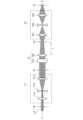
- FIG. 1 is a perspective view schematically showing the configuration of a laser annealing device. Only the main optical system of the laser annealing apparatus shown in FIG. 1 is extracted and schematically shown. An example of the configuration of an optical system (beam adjustment device) of a laser annealing device is schematically shown. A specific example of adjusting the distance between lenses will be shown.
- FIG. 1 is a perspective view schematically showing the configuration of a laser annealing apparatus 1.
- the laser annealing apparatus 1 is an apparatus that performs an annealing process (heating process) by irradiating a semiconductor wafer 3 with a laser pulse as a laser beam oscillated by a pulsed laser apparatus 2 as a laser apparatus.
- the laser device is not limited to the pulse laser device 2, and may be any other type of laser device.
- the laser device may be a continuous wave (CW) laser device or a diode laser device.
- CW continuous wave
- the semiconductor wafer 3 fixedly mounted on the wafer table 31 can be driven integrally with the wafer table 31 in the illustrated x direction by a stage device 4, which will be described later. Further, the laser pulse (laser light) oscillated by the pulse laser device 2 can be scanned in the y direction orthogonal to the x direction by a galvano scanner 14, which will be described later. Laser pulses (laser light) scanned in the y direction by the galvano scanner 14 are reflected by a mirror 16, which will be described later, and are incident on the semiconductor wafer 3 in the z direction orthogonal to the x and y directions.
- the x direction which is the driving direction of the semiconductor wafer 3 is parallel to the X-axis direction (X direction)
- the y direction which is the scanning direction of the laser pulse (laser light)
- the z direction which is the direction of incidence of the laser pulse (laser light) on the wafer 3, is parallel to the Z-axis direction (Z direction).
- the x direction and the X direction will also be referred to as the vertical direction
- the y direction and the Y direction will also be referred to as the horizontal direction
- the z direction and the Z direction will also be referred to as the height direction.
- the pulse laser device 2 is a laser device that oscillates laser pulses LP at a frequency of 100kHz or higher.
- the frequency of the laser pulse LP emitted by the pulse laser device 2 is, for example, between 100 kHz and 10 MHz, preferably between 500 kHz and 5 MHz, and more preferably between 700 kHz and 3 MHz.
- the pulse laser device 2 is configured, for example, by a fiber laser device that oscillates a laser pulse LP using an optical fiber.
- a laser pulse LP as a laser beam is emitted from an output point OP of the pulse laser device 2 in the X direction.
- a laser annealing apparatus 1 that guides this laser pulse LP to a semiconductor wafer 3 to be irradiated includes a beam expander 11, a mirror 12, a beam shaping optical system 13, a galvano scanner 14, a zoom optical system 15, and a mirror 16. Be prepared.
- the beam expander 11 as a beam size adjustment section adjusts the laser pulse LP (laser light) emitted from the output point OP of the pulse laser device 2 to a predetermined size (diameter). For example, when the cross section of the laser pulse LP (laser light) emitted from the output point OP of the pulse laser device 2 is approximately circular with a diameter D0 (initial size), the beam expander 11 Convert (typically enlarge) the cross section of into a substantially circular shape with a predetermined diameter D1 (input size).
- the beam expander 11 is composed of a plurality of lenses 111, 112, and 113.
- the first lens 111 is a convex lens
- the second lens 112 is a concave lens
- the third lens 113 is a convex lens.
- the number and type of lenses and other optical elements constituting the beam expander 11 are arbitrary as long as the desired function and/or effect of adjusting the size of the laser pulse LP can be obtained.
- the beam expander 11 may be composed of two or more convex lenses and one or more concave lenses arranged in any order, or may be composed only of three or more convex lenses.
- the mirror 12 reflects the laser pulse LP whose size has been adjusted by the beam expander 11, and changes its traveling direction from the X direction to the Y direction.
- the beam shaping optical system 13 is a beam shaping section that shapes the laser pulse LP whose size has been adjusted by the beam expander 11 to adjust its shape and/or intensity distribution.
- the cross section of the laser pulse LP whose size has been adjusted by the beam expander 11 is approximately circular and has an intensity distribution that follows a Gaussian distribution or a normal distribution, but is shaped by the beam shaping optical system 13 to be approximately rectangular and have an approximately uniform intensity distribution. be done.
- a beam shaping optical system 13 includes, for example, a beam shaping optical element 131 such as a diffractive optical element (DOE) or an aspherical optical element having an aspherical surface that is neither flat nor spherical, and an intermediate imaging lens. 132.
- DOE diffractive optical element
- the galvano scanner 14 is a beam scanning unit that scans the laser pulse LP shaped by the beam shaping optical system 13 along the y direction (Y direction).
- the galvano scanner 14 includes a galvano mirror 141 as a drivable optical element that reflects an incident laser pulse LP and directs it to a desired scanning position in the y direction, and a motor 142 that rotates the galvano mirror 141 around the Z axis. Equipped with.
- the motor 142 adjusts the rotational position or rotational angle of the galvano mirror 141 around the Z axis, so that the laser pulse LP incident on the galvano mirror 141 is reflected to an arbitrary position in the y direction.
- the beam scanning unit that directs the incident laser pulse LP to a desired scanning position in the y direction is not limited to the galvano scanner 14, but may also be a polygon mirror scanner equipped with a polygon mirror (optical element) that can be rotated or a driveable MEMS. (Micro Electro Mechanical Systems) May be configured by optical elements such as mirrors.
- the scanning direction of the laser pulse LP by the beam scanning unit such as the galvano scanner 14 is not limited to the y direction (Y direction), but may also be a direction intersecting the y direction (Y direction) such as the x direction (X direction), It may be in two directions, the x direction (X direction) and the y direction (Y direction).
- the beam scanning unit such as the galvano scanner 14 can scan the laser pulse LP within the xy plane (XY plane), that is, within the plane of the semiconductor wafer 3, the semiconductor wafer 3 and the wafer table 31 are moved in the x direction. It is not necessary to provide the stage device 4 that is driven in the (X direction) or the like. In this case, the galvano scanner 14 and the like constitute a biaxial beam scanning section in the X direction and the Y direction.
- the zoom optical system 15 includes a convex lens 151, a concave lens 152, and an imaging lens 153 arranged before and after the galvano scanner 14.
- a convex lens 151 and a concave lens 152 are arranged before the galvano scanner 14, and an imaging lens 153 is arranged after the galvano scanner 14.
- the imaging lens 153 together with the convex lens 151 and the concave lens 152, focuses the laser pulse LP scanned in the y direction (Y direction) by the galvano scanner 14 onto the semiconductor wafer 3 to be annealed.
- a mirror 16 provided between the imaging lens 153 and the semiconductor wafer 3 reflects the laser pulse LP in the X direction from the imaging lens 153 and irradiates the semiconductor wafer 3 in the Z direction (z direction).
- the laser pulse LP thus focused on the semiconductor wafer 3 by the imaging lens 153 and the mirror 16 moves in the Y direction within the plane of the semiconductor wafer 3 by scanning in the Y direction by the galvano scanner 14.
- the size of the laser pulse LP focused on the semiconductor wafer 3 (irradiation size Dv) can be arbitrarily designed, but it is preferably between 0.10 mm square and 0.15 mm square, and between 0.12 mm square and 0.13 mm square. It is even more preferable.
- the scanning speed of the laser pulse LP in the Y direction on the semiconductor wafer 3 surface (and/or the driving speed of the semiconductor wafer 3 in the X direction by the stage device 4) can be arbitrarily designed; for example, 100 cm/s and 500 cm. It is preferably between 250 cm/s and 350 cm/s, more preferably between 250 cm/s and 350 cm/s.
- the stage device 4 is a drive device that drives the semiconductor wafer 3 and the wafer table 31 relative to the laser pulse LP along the x direction (X direction). ) constitutes a beam scanning unit that scans the laser pulse LP along the By this stage device 4, the laser pulse LP is relatively moved in the X direction within the surface of the semiconductor wafer 3.
- the laser pulse LP can be scanned within the xy plane (XY plane), that is, within the three surfaces of the semiconductor wafer.
- the driving direction of the semiconductor wafer 3 by the stage device 4 is not limited to the x direction (X direction), but may also be a direction intersecting the x direction (X direction) such as the y direction (Y direction), or a direction intersecting the x direction (X direction) such as the y direction (Y direction).
- the stage device 4 when the stage device 4 can drive the semiconductor wafer 3 relative to the laser pulse LP within the xy plane (XY plane), a galvanometer that scans the laser pulse LP in the y direction (Y direction) etc.
- the scanner 14 may not be provided.
- the stage device 4 constitutes a biaxial beam scanning section in the X direction and the Y direction.
- FIG. 2 schematically shows only the main optical system of the laser annealing apparatus 1 shown in FIG. 1.
- the cross section of the laser pulse LP (laser light) emitted by the pulse laser device 2 is approximately circular and has an intensity distribution that follows a Gaussian distribution or a normal distribution, and its size (diameter) is the initial size D0.
- the beam expander 11 changes the size (diameter) from the initial size D0 to a diffractive optical element or the like while maintaining the shape (approximately circular) and intensity distribution (Gaussian distribution) of the laser pulse LP provided from the pulse laser device 2.
- the input size is converted (typically enlarged) to the input size D1 determined by the specifications of the beam shaping optical element 131. Furthermore, in accordance with the specifications of the beam shaping optical element 131 such as a diffractive optical element, the divergence angle of the laser pulse LP of input size D1 formed by the beam expander 11 is zero.
- a beam shaping optical element 131 such as a diffractive optical element shapes the shape of the laser pulse LP provided from the beam expander 11 from a substantially circular shape to a substantially rectangular shape, and also adjusts the intensity distribution from a Gaussian distribution to a substantially uniform intensity distribution.
- the substantially rectangular laser pulse LP having such a substantially uniform intensity distribution is focused with an output size D2 at an imaging position f located at a certain distance from the intermediate imaging lens 132 disposed after the beam shaping optical element 131. imaged. Not only the above-mentioned input size D1 but also the output size D2 are strictly determined by the specifications of the beam shaping optical element 131 such as a diffractive optical element.
- a zoom optical system 15 provided after the imaging position f of the beam shaping optical system 13 adjusts the size (diameter) of the substantially rectangular laser pulse LP having a substantially uniform intensity distribution shaped by the beam shaping optical system 13.
- the output size D2 is converted into an irradiation size Dv suitable for annealing the semiconductor wafer 3.
- the laser pulse LP oscillated by the pulse laser apparatus 2 is adjusted according to the specifications. It is necessary to provide a beam size adjusting unit such as a beam expander 11 at the front stage of the beam shaping optical system 13 to adjust the input size D1 to the input size D1 based on the specifications, and to adjust the laser pulse LP with the output size D2 based on the specification to the desired irradiation size Dv. It is necessary to provide the zoom optical system 15 for conversion after the beam shaping optical system 13. The beam expander 11 and zoom optical system 15 make the laser annealing apparatus 1 large and/or expensive. Further, it is complicated because it is necessary to adjust the beam expander 11 and the zoom optical system 15 individually.
- FIG. 3 schematically shows a configuration example of the optical system (beam adjustment device) of the laser annealing apparatus 1 to solve such problems.
- the zoom optical system 15 in FIG. 2 is not provided, and the system is substantially composed of a beam expander 11 as a beam size adjustment section, a beam shaping optical element 131 such as a diffractive optical element, and an intermediate imaging lens 132.
- the beam shaping optical system 13 constitutes the optical system of the laser annealing apparatus 1.
- the beam expander 11 maintains the shape (approximately circular) and intensity distribution (Gaussian distribution) of the laser pulse LP of initial size D0 provided from the pulse laser device 2, while maintaining the shape determined by the specifications of the beam shaping optical element 131.
- the size Dx is adjusted to be different from the input size D1 (FIG. 2).
- the laser pulse LP adjusted to the size Dx ( ⁇ D1) by the beam expander 11 does not conform to the specifications of the beam shaping optical element 131 such as a diffractive optical element, and is transferred from the beam expander 11 to the beam shaping optical element 131. It has a non-zero divergence angle ⁇ x with respect to the direction toward which it is directed.
- the divergence angle ⁇ x can be adjusted to a desired size depending on the distance between the lenses in the beam expander 11, but it is typically preferable to set it between 1 mrad and 10 mrad ( ⁇ x in FIG. 3). are exaggerated for visualization). Due to the non-zero divergence angle ⁇ x, the size (diameter) of the laser pulse LP monotonically increases or decreases from the beam expander 11 (third lens 113) toward the beam shaping optical element 131. As illustrated, the size Dx is the size (diameter) of the laser pulse LP at the incident surface of the beam shaping optical element 131.
- a beam shaping optical element 131 such as a diffractive optical element shapes the shape of the laser pulse LP having a divergence angle ⁇ x and a size Dx provided from the beam expander 11 from a substantially circular shape to a substantially rectangular shape, and also changes the intensity from a Gaussian distribution to a substantially uniform intensity. Adjust to distribution.
- the substantially rectangular laser pulse LP having such a substantially uniform intensity distribution has a variable irradiation size Dv at an imaging position f located at a constant distance from the intermediate imaging lens 132 disposed after the beam shaping optical element 131.
- the image is formed by This irradiation size Dv is typically different from the output size D2 (FIG. 2) defined in the specifications of the beam shaping optical element 131.
- the laser pulse LP adjusted to the variable irradiation size Dv by the beam shaping optical element 131 is applied to the semiconductor wafer 3 placed near the imaging position f (using the zoom optical system 15 as shown in FIG. 2). irradiated directly (without intervention).
- Two main parameters are the distance L2 between the second lenses.
- the size (Dx and/or Dv) of the laser pulse LP is adjusted mainly by adjusting the first inter-lens distance L1.
- the size of the laser pulse LP emitted from the beam expander 11 to the beam shaping optical element 131 deviates from the specification value D1 (FIG. 2).
- the irradiation size Dv when the irradiation size Dv is smaller than the specification value D2, there will be a "convex" non-uniform intensity distribution in which the intensity at the center is greater than the intensity at the periphery, and the irradiation size Dv will be smaller than the specification value D2. If it is large, a "concave" non-uniform intensity distribution will result, with the intensity at the center being smaller than the intensity at the periphery.
- the non-zero divergence angle ⁇ x is adjusted mainly by adjusting the distance L2 between the second lenses.
- Such a non-zero divergence angle ⁇ x is also “out of specification” for the beam shaping optical element 131, but together with the size Dx ( ⁇ D1), which is also “out of specification”, it results in a typical deviation in laser annealing, etc. It was found that it is possible to realize an irradiation beam of a quality that is practically acceptable for various purposes and targets.
- the distance L1 between the first lenses is set in two ways, 64 mm and 150 mm, to form irradiation beams with different irradiation sizes Dv, and the distance L2 between the second lenses is adjusted appropriately to increase the intensity.
- a specific example of improving the uniformity of distribution will be shown.
- the accuracy of shape, intensity distribution, size, etc. is lower, but the quality is acceptable for practical use
- the irradiation beam can be realized without the zoom optical system 15 (FIG. 2)
- the laser annealing apparatus 1 can be configured in a small size and at low cost. Further, by simply adjusting the distance between the lenses 111 to 113 constituting the beam expander 11, both the beam shaping accuracy by the beam shaping optical system 13 and the irradiation size Dv can be efficiently adjusted.
- Adjustment of the optical system as described above, specifically adjustment of the distance between the lenses 111 to 113 that constitute the beam expander 11, is automatically performed by an optical sensor 51 such as a camera and an inter-lens distance adjustment section 52. You can.
- the optical sensor 51 detects the shape, intensity distribution, size, etc. of the irradiation beam on the semiconductor wafer 3, and the inter-lens distance adjustment unit 52 adjusts the beam expander so that the beam has the desired shape, intensity distribution, size, etc.
- the distance between lenses 111 to 113 constituting lens 11 is automatically adjusted.
- the size of the laser pulse LP was mainly adjusted by the distance L1 between the first lenses, and the divergence angle ⁇ x (that is, the uniformity of the intensity distribution) was mainly adjusted by the distance L2 between the second lenses.
- the divergence angle ⁇ x may be adjusted by the first inter-lens distance L1, and the size may be adjusted mainly by the second inter-lens distance L2.
- desired parameters shape, intensity distribution, size
- the third inter-lens distance between the first lens 111 and the third lens may be used as an adjustment parameter.
- the convex lens as the first lens 111, the concave lens as the second lens 112, and the convex lens as the third lens 113 are arranged in the order in which the laser pulse LP passes.
- the type (convex lens, concave lens, etc.), number, and arrangement order of the lenses are arbitrary as long as the above operations and/or effects of this embodiment are achieved.
- the beam expander 11 only needs to be composed of at least three lenses including at least two convex lenses, and the arrangement order thereof is arbitrary.
- the beam expander 11 may be configured with two or more convex lenses and one or more concave lenses, or the beam expander 11 may be configured with three or more convex lenses. good.
- each device and each method described in the embodiments can be realized by hardware resources or software resources, or by cooperation of hardware resources and software resources.
- hardware resources for example, a processor, ROM, RAM, and various integrated circuits can be used.
- software resources for example, programs such as operating systems and applications can be used.
- the present invention relates to a laser annealing device and the like.
- 1 Laser annealing device 2 Pulse laser device, 3 Semiconductor wafer, 4 Stage device, 11 Beam expander, 13 Beam shaping optical system, 14 Galvano scanner, 15 Zoom optical system, 51 Optical sensor, 52 Inter-lens distance adjustment section, 111 First lens, 112 Second lens, 113 Third lens, 131 Beam shaping optical element, 132 Intermediate imaging lens, L1 Distance between first lenses, L2 Distance between second lenses, LP Laser pulse.
Landscapes
- Physics & Mathematics (AREA)
- Optics & Photonics (AREA)
- Engineering & Computer Science (AREA)
- Plasma & Fusion (AREA)
- Mechanical Engineering (AREA)
- Recrystallisation Techniques (AREA)
- Lasers (AREA)
- Lenses (AREA)
Abstract
Ce dispositif de réglage de faisceau comprend : un dilatateur de faisceau (11) qui ajuste la taille d'une impulsion laser (LP) à l'aide d'une première lentille (111), d'une deuxième lentille (112) et d'une troisième lentille (113), qui comprend au moins deux lentilles convexes ; et un élément optique de mise en forme de faisceau (131) qui met en forme la section transversale de l'impulsion laser (LP) dont la taille a été ajustée par le dilatateur de faisceau (11). L'impulsion laser (LP) dont la taille a été ajustée par le dilatateur de faisceau (11) a un angle de divergence non nul thêta_x par rapport à la direction allant du dilatateur de faisceau (11) vers l'élément optique de mise en forme de faisceau (131).
Applications Claiming Priority (2)
| Application Number | Priority Date | Filing Date | Title |
|---|---|---|---|
| JP2022114797 | 2022-07-19 | ||
| JP2022-114797 | 2022-07-19 |
Publications (1)
| Publication Number | Publication Date |
|---|---|
| WO2024018785A1 true WO2024018785A1 (fr) | 2024-01-25 |
Family
ID=89617564
Family Applications (1)
| Application Number | Title | Priority Date | Filing Date |
|---|---|---|---|
| PCT/JP2023/022019 Ceased WO2024018785A1 (fr) | 2022-07-19 | 2023-06-14 | Dispositif de réglage de faisceau et dispositif de recuit par laser |
Country Status (2)
| Country | Link |
|---|---|
| TW (1) | TWI850026B (fr) |
| WO (1) | WO2024018785A1 (fr) |
Citations (5)
| Publication number | Priority date | Publication date | Assignee | Title |
|---|---|---|---|---|
| JP2007214554A (ja) * | 2006-01-12 | 2007-08-23 | Semiconductor Energy Lab Co Ltd | レーザー光照射装置、レーザー光照射方法並びに半導体装置の作製方法 |
| JP2008098621A (ja) * | 2006-09-14 | 2008-04-24 | Semiconductor Energy Lab Co Ltd | レーザ光照射装置およびレーザ光照射方法 |
| JP2008181918A (ja) * | 2007-01-23 | 2008-08-07 | Ihi Corp | レーザビームの形状制御装置 |
| US20090323739A1 (en) * | 2006-12-22 | 2009-12-31 | Uv Tech Systems | Laser optical system |
| JP2021197521A (ja) * | 2020-06-18 | 2021-12-27 | 住友重機械工業株式会社 | レーザ処理方法、レーザ処理装置の制御装置、及びレーザ処理装置 |
Family Cites Families (3)
| Publication number | Priority date | Publication date | Assignee | Title |
|---|---|---|---|---|
| CN102135665A (zh) * | 2011-04-01 | 2011-07-27 | 北京工业大学 | 将高斯光束整形为平顶光束的装置和方法 |
| CN104991347A (zh) * | 2015-07-16 | 2015-10-21 | 哈尔滨工业大学 | 基于微透镜阵列的激光整形照明器 |
| WO2021256434A1 (fr) * | 2020-06-18 | 2021-12-23 | 住友重機械工業株式会社 | Dispositif de commande d'appareil de recuit au laser et procédé de recuit au laser |
-
2023
- 2023-06-14 WO PCT/JP2023/022019 patent/WO2024018785A1/fr not_active Ceased
- 2023-07-17 TW TW112126489A patent/TWI850026B/zh active
Patent Citations (5)
| Publication number | Priority date | Publication date | Assignee | Title |
|---|---|---|---|---|
| JP2007214554A (ja) * | 2006-01-12 | 2007-08-23 | Semiconductor Energy Lab Co Ltd | レーザー光照射装置、レーザー光照射方法並びに半導体装置の作製方法 |
| JP2008098621A (ja) * | 2006-09-14 | 2008-04-24 | Semiconductor Energy Lab Co Ltd | レーザ光照射装置およびレーザ光照射方法 |
| US20090323739A1 (en) * | 2006-12-22 | 2009-12-31 | Uv Tech Systems | Laser optical system |
| JP2008181918A (ja) * | 2007-01-23 | 2008-08-07 | Ihi Corp | レーザビームの形状制御装置 |
| JP2021197521A (ja) * | 2020-06-18 | 2021-12-27 | 住友重機械工業株式会社 | レーザ処理方法、レーザ処理装置の制御装置、及びレーザ処理装置 |
Also Published As
| Publication number | Publication date |
|---|---|
| TW202405907A (zh) | 2024-02-01 |
| TWI850026B (zh) | 2024-07-21 |
Similar Documents
| Publication | Publication Date | Title |
|---|---|---|
| JP6977609B2 (ja) | 光照射装置、光照射装置を用いた光加工装置、光照射方法、及び光加工方法 | |
| KR101647279B1 (ko) | 마이크로렌즈 어레이를 이용하여 라인을 생성하기 위한 광학적 설계 | |
| KR100500343B1 (ko) | 레이저 가공 장치 | |
| JP4401410B2 (ja) | レーザ加工装置 | |
| KR100487085B1 (ko) | 조명광학계 및 이를 구비하는 레이저 처리장치 | |
| KR20150126603A (ko) | 테이퍼 제어를 위한 빔 각도 및 작업물 이동의 공조 | |
| KR101857544B1 (ko) | 레이저 광학 장치 및 헤드 | |
| JP2009082958A (ja) | レーザ加工装置及びアキシコンレンズ | |
| KR102483670B1 (ko) | 레이저 가공 시스템 및 레이저 가공 방법 | |
| KR102050765B1 (ko) | 3차원 고속 정밀 레이저 가공 장치 | |
| WO2022185721A1 (fr) | Dispositif de traitement au laser | |
| TWI871387B (zh) | 雷射照射裝置 | |
| WO2024018785A1 (fr) | Dispositif de réglage de faisceau et dispositif de recuit par laser | |
| KR101519920B1 (ko) | 프린팅롤 미세패턴 형성장치 및 형성방법 | |
| JP7629087B2 (ja) | 作業面上に規定のレーザラインを生成するための装置 | |
| JP2001075043A (ja) | 精密可変型長尺ビーム光学系 | |
| JP2007029959A (ja) | レーザ加工機 | |
| JP4818958B2 (ja) | ビーム照射装置、及び、ビーム照射方法 | |
| CN114388388B (en) | Laser annealing device and laser annealing method | |
| JP3781091B2 (ja) | ビーム整形装置 | |
| KR20100049393A (ko) | 드릴링 장치 및 드릴링 방법 | |
| JP3524855B2 (ja) | レーザ照射装置及びレーザ加工方法 | |
| TW202043849A (zh) | 在工作平面上產生線性強度分佈的裝置 | |
| KR20160140212A (ko) | 레이저 가공장치 및 레이저 가공방법 | |
| KR102724285B1 (ko) | 대물렌즈를 이용한 레이저 가공 장치 및 그의 동작 방법 |
Legal Events
| Date | Code | Title | Description |
|---|---|---|---|
| 121 | Ep: the epo has been informed by wipo that ep was designated in this application |
Ref document number: 23842717 Country of ref document: EP Kind code of ref document: A1 |
|
| NENP | Non-entry into the national phase |
Ref country code: DE |
|
| 122 | Ep: pct application non-entry in european phase |
Ref document number: 23842717 Country of ref document: EP Kind code of ref document: A1 |
|
| NENP | Non-entry into the national phase |
Ref country code: JP |