WO2024116827A1 - SiC成形体及びSiC成形体の製造方法 - Google Patents
SiC成形体及びSiC成形体の製造方法 Download PDFInfo
- Publication number
- WO2024116827A1 WO2024116827A1 PCT/JP2023/040933 JP2023040933W WO2024116827A1 WO 2024116827 A1 WO2024116827 A1 WO 2024116827A1 JP 2023040933 W JP2023040933 W JP 2023040933W WO 2024116827 A1 WO2024116827 A1 WO 2024116827A1
- Authority
- WO
- WIPO (PCT)
- Prior art keywords
- sic
- gas
- molded body
- reaction chamber
- substrate
- Prior art date
- Legal status (The legal status is an assumption and is not a legal conclusion. Google has not performed a legal analysis and makes no representation as to the accuracy of the status listed.)
- Ceased
Links
Classifications
-
- C—CHEMISTRY; METALLURGY
- C23—COATING METALLIC MATERIAL; COATING MATERIAL WITH METALLIC MATERIAL; CHEMICAL SURFACE TREATMENT; DIFFUSION TREATMENT OF METALLIC MATERIAL; COATING BY VACUUM EVAPORATION, BY SPUTTERING, BY ION IMPLANTATION OR BY CHEMICAL VAPOUR DEPOSITION, IN GENERAL; INHIBITING CORROSION OF METALLIC MATERIAL OR INCRUSTATION IN GENERAL
- C23C—COATING METALLIC MATERIAL; COATING MATERIAL WITH METALLIC MATERIAL; SURFACE TREATMENT OF METALLIC MATERIAL BY DIFFUSION INTO THE SURFACE, BY CHEMICAL CONVERSION OR SUBSTITUTION; COATING BY VACUUM EVAPORATION, BY SPUTTERING, BY ION IMPLANTATION OR BY CHEMICAL VAPOUR DEPOSITION, IN GENERAL
- C23C16/00—Chemical coating by decomposition of gaseous compounds, without leaving reaction products of surface material in the coating, i.e. chemical vapour deposition [CVD] processes
- C23C16/22—Chemical coating by decomposition of gaseous compounds, without leaving reaction products of surface material in the coating, i.e. chemical vapour deposition [CVD] processes characterised by the deposition of inorganic material, other than metallic material
- C23C16/30—Deposition of compounds, mixtures or solid solutions, e.g. borides, carbides, nitrides
- C23C16/42—Silicides
-
- C—CHEMISTRY; METALLURGY
- C23—COATING METALLIC MATERIAL; COATING MATERIAL WITH METALLIC MATERIAL; CHEMICAL SURFACE TREATMENT; DIFFUSION TREATMENT OF METALLIC MATERIAL; COATING BY VACUUM EVAPORATION, BY SPUTTERING, BY ION IMPLANTATION OR BY CHEMICAL VAPOUR DEPOSITION, IN GENERAL; INHIBITING CORROSION OF METALLIC MATERIAL OR INCRUSTATION IN GENERAL
- C23C—COATING METALLIC MATERIAL; COATING MATERIAL WITH METALLIC MATERIAL; SURFACE TREATMENT OF METALLIC MATERIAL BY DIFFUSION INTO THE SURFACE, BY CHEMICAL CONVERSION OR SUBSTITUTION; COATING BY VACUUM EVAPORATION, BY SPUTTERING, BY ION IMPLANTATION OR BY CHEMICAL VAPOUR DEPOSITION, IN GENERAL
- C23C16/00—Chemical coating by decomposition of gaseous compounds, without leaving reaction products of surface material in the coating, i.e. chemical vapour deposition [CVD] processes
- C23C16/22—Chemical coating by decomposition of gaseous compounds, without leaving reaction products of surface material in the coating, i.e. chemical vapour deposition [CVD] processes characterised by the deposition of inorganic material, other than metallic material
- C23C16/30—Deposition of compounds, mixtures or solid solutions, e.g. borides, carbides, nitrides
- C23C16/32—Carbides
- C23C16/325—Silicon carbide
-
- C—CHEMISTRY; METALLURGY
- C23—COATING METALLIC MATERIAL; COATING MATERIAL WITH METALLIC MATERIAL; CHEMICAL SURFACE TREATMENT; DIFFUSION TREATMENT OF METALLIC MATERIAL; COATING BY VACUUM EVAPORATION, BY SPUTTERING, BY ION IMPLANTATION OR BY CHEMICAL VAPOUR DEPOSITION, IN GENERAL; INHIBITING CORROSION OF METALLIC MATERIAL OR INCRUSTATION IN GENERAL
- C23C—COATING METALLIC MATERIAL; COATING MATERIAL WITH METALLIC MATERIAL; SURFACE TREATMENT OF METALLIC MATERIAL BY DIFFUSION INTO THE SURFACE, BY CHEMICAL CONVERSION OR SUBSTITUTION; COATING BY VACUUM EVAPORATION, BY SPUTTERING, BY ION IMPLANTATION OR BY CHEMICAL VAPOUR DEPOSITION, IN GENERAL
- C23C16/00—Chemical coating by decomposition of gaseous compounds, without leaving reaction products of surface material in the coating, i.e. chemical vapour deposition [CVD] processes
- C23C16/44—Chemical coating by decomposition of gaseous compounds, without leaving reaction products of surface material in the coating, i.e. chemical vapour deposition [CVD] processes characterised by the method of coating
- C23C16/52—Controlling or regulating the coating process
-
- C—CHEMISTRY; METALLURGY
- C23—COATING METALLIC MATERIAL; COATING MATERIAL WITH METALLIC MATERIAL; CHEMICAL SURFACE TREATMENT; DIFFUSION TREATMENT OF METALLIC MATERIAL; COATING BY VACUUM EVAPORATION, BY SPUTTERING, BY ION IMPLANTATION OR BY CHEMICAL VAPOUR DEPOSITION, IN GENERAL; INHIBITING CORROSION OF METALLIC MATERIAL OR INCRUSTATION IN GENERAL
- C23C—COATING METALLIC MATERIAL; COATING MATERIAL WITH METALLIC MATERIAL; SURFACE TREATMENT OF METALLIC MATERIAL BY DIFFUSION INTO THE SURFACE, BY CHEMICAL CONVERSION OR SUBSTITUTION; COATING BY VACUUM EVAPORATION, BY SPUTTERING, BY ION IMPLANTATION OR BY CHEMICAL VAPOUR DEPOSITION, IN GENERAL
- C23C16/00—Chemical coating by decomposition of gaseous compounds, without leaving reaction products of surface material in the coating, i.e. chemical vapour deposition [CVD] processes
- C23C16/56—After-treatment
Definitions
- This disclosure relates to a SiC compact and a method for manufacturing a SiC compact.
- SiC compacts One important property of silicon carbide (SiC) compacts is their electrical properties. For example, various SiC compacts with specific resistivities have been proposed.
- Patent Document 1 discloses a silicon carbide body obtained by a CVD method.
- the silicon carbide body contains 0.1 to 100 ppm of nitrogen element and has a resistivity of 0.01 to 10 ⁇ cm. Furthermore, the content of metal elements other than silicon is 10 ppm or less.
- Patent Document 2 discloses a polycrystalline SiC compact with a resistivity of 0.050 ⁇ cm or less.
- the objective of this disclosure is to provide a low-resistance SiC molded body and a method for manufacturing said SiC molded body.
- the present disclosure includes the following embodiments.
- ⁇ 1> A SiC molded body having a volume resistivity of 7.0 ⁇ 10 ⁇ 3 ⁇ cm or less and a nitrogen concentration in the range of more than 1000 ppm and not more than 4500 ppm.
- ⁇ 2> The SiC molded body according to ⁇ 1>, having a ratio of CN peak intensity to SiN peak intensity of 1.2 or more as measured by time-of-flight secondary ion mass spectrometry.
- ⁇ 3> The SiC molded body according to ⁇ 1> or ⁇ 2>, wherein the volume resistivity is 5.0 ⁇ 10 ⁇ 3 ⁇ cm or less.
- a method for producing a SiC molded body according to ⁇ 1> comprising: preparing a substrate in a reaction chamber; supplying a source gas containing silicon and carbon, a nitrogen-containing dopant gas, a carrier gas, and hydrogen chloride gas into the reaction chamber to form a SiC film on the substrate; and removing the substrate from the SiC film, wherein a partial pressure of the hydrogen chloride gas in the reaction chamber during the process of forming the SiC film is 1000 Pa or more.
- a low-resistance SiC molded body is provided.
- ordinal numbers e.g., “first” and “second” are terms used to distinguish elements and do not limit the quantity, order, or superiority of the elements.
- the SiC compact according to one embodiment of the present disclosure has the following characteristics.
- the volume resistivity of the SiC compact is 7.0 ⁇ 10 ⁇ cm or less, and the nitrogen concentration in the SiC compact is in the range of more than 1000 ppm and not more than 4500 ppm.
- a low-resistance SiC compact is provided.
- the SiC compact is preferably a polycrystalline SiC compact.
- the volume resistivity of the SiC molded body is 7.0 ⁇ 10 ⁇ 3 ⁇ cm or less.
- the volume resistivity of the SiC molded body is preferably 5.0 ⁇ 10 ⁇ 3 ⁇ cm or less, more preferably 3.0 ⁇ 10 ⁇ 3 ⁇ cm or less, and even more preferably 1.0 ⁇ 10 ⁇ 3 ⁇ cm or less.
- a low-resistance SiC molded body is suitable for use in a plasma etching device member.
- the lower limit of the volume resistivity is not limited.
- the lower limit of the volume resistivity may be 0.1 ⁇ 10 ⁇ 3 ⁇ cm, 0.3 ⁇ 10 ⁇ 3 ⁇ cm, or 0.5 ⁇ 10 ⁇ 3 ⁇ cm.
- the volume resistivity may be in the range of 0.1 ⁇ 10 ⁇ 3 ⁇ cm to 7.0 ⁇ 10 ⁇ 3 ⁇ cm.
- the volume resistivity is measured by a four-probe method.
- An example of the measuring device is "Loresta GP MCT-T610" (Mitsubishi Chemical Analytech Co., Ltd.).
- the nitrogen concentration in the SiC compact is in the range of more than 1000 ppm and not more than 4500 ppm. As the nitrogen concentration in the SiC compact increases, the volume resistivity tends to decrease. From the viewpoint of reducing the volume resistivity, the nitrogen concentration is preferably 1500 ppm or more, more preferably 2000 ppm or more, and even more preferably 2500 ppm or more. The upper limit of the nitrogen concentration may be 4000 ppm, 3500 ppm, or 3000 ppm. In the present disclosure, the nitrogen concentration is measured by secondary ion mass spectrometry (SIMS).
- SIMS secondary ion mass spectrometry
- TOF-SIMS time-of-flight secondary ion mass spectrometry
- TOF-SIMS is a method of analyzing the surface of a solid sample by irradiating a solid sample with primary ions and detecting secondary ions emitted from the surface of the solid sample.
- the "ratio of the CN -peak intensity to the SiN -peak intensity” is referred to as the "CN - /SiN -peak intensity ratio”.
- the CN - /SiN -peak intensity ratio is preferably 1 or more, more preferably 1.2 or more, and even more preferably 1.5 or more. Furthermore, the CN - /SiN -peak intensity ratio is preferably 2.0 or more, and more preferably 2.5 or more.
- the reason for the decrease in the volume resistivity has not been completely elucidated, it is presumed that the decrease in the volume resistivity is due to the following difference in crystal structure. In general, it is believed that nitrogen (N) introduced into SiC preferentially occupies the carbon (C) position compared to the silicon (Si) position in the SiC crystal. In this case, the CN - /SiN -peak intensity ratio tends to be smaller.
- the upper limit of the CN - /SiN -peak intensity ratio is not limited.
- the upper limit of the CN - /SiN -peak intensity ratio may be 3.0 or 4.0.
- the CN - /SiN -peak intensity ratio may be within the range of 1.0 to 4.0.
- the Si:C molar ratio in the SiC compact is preferably 49.00:51.00 to 51.00:49.00, and more preferably 49.50:50.50 to 50.50:49.50.
- the Si:C molar ratio is measured by secondary ion mass spectrometry (SIMS).
- the shape of the SiC molded body is not limited. The shape of the SiC molded body may be determined taking into consideration the application.
- the SiC molded body may be a flat SiC molded body.
- the SiC molded body may be a disk-shaped, ring-shaped, cylindrical or rod-shaped SiC molded body.
- An example of an application of a disk-shaped or ring-shaped SiC molded body is a semiconductor component.
- An example of an application of a cylindrical or rod-shaped SiC molded body is a heater component.
- the thickness of the SiC compact is not limited. The thickness of the SiC compact may be determined taking into consideration the application.
- the thickness of the SiC compact may be at least 0.15 mm.
- the thickness of the SiC compact may be at least 0.35 mm.
- the thickness of the SiC compact may be at least 4 mm.
- the thickness of the SiC compact may be in the range of 0.1 mm to 5 mm.
- the thickness of the SiC compact may be in the range of 0.2 mm to 3 mm.
- SiC molded bodies are not limited. Examples of uses of SiC molded bodies include semiconductor manufacturing equipment components. Examples of semiconductor manufacturing equipment include plasma etching equipment and heat treatment equipment. Examples of plasma etching equipment components include edge rings, electrode plates, and heaters. Examples of heat treatment equipment components include dummy wafers. Examples of uses of SiC molded bodies include reaction chamber components for thin film formation equipment. Examples of thin film formation equipment include CVD equipment. CVD is an abbreviation for Chemical Vapor Deposition.
- the manufacturing method of the SiC molded body is not limited.
- the SiC molded body is manufactured by utilizing chemical vapor deposition.
- the manufacturing method of the SiC molded body includes (1) preparing a substrate in a reaction chamber, (2) supplying a source gas containing silicon and carbon, a nitrogen-containing dopant gas, and a carrier gas into the reaction chamber to form a SiC film on the substrate, and (3) removing the substrate from the SiC film. Each step is described below.
- Step (1) includes preparing a substrate in a reaction chamber.
- One or more substrates may be placed in one reaction chamber.
- the reaction chamber defines a space for carrying out a reaction to form a SiC film on a substrate.
- the thin film forming apparatus including the reaction chamber may be selected from known CVD apparatuses.
- the CVD apparatus may be a hot-wall type CVD apparatus or a cold-wall type CVD apparatus.
- the substrate is preferably a graphite substrate.
- the shape and dimensions of the substrate may be determined taking into account the shape and dimensions of the desired SiC film.
- the substrate may be a disk-shaped substrate.
- the thickness of the substrate may be in the range of 0.5 mm to 100 mm.
- Step (2) involves supplying a source gas containing both silicon and carbon, a nitrogen-containing dopant gas, and a carrier gas into a reaction chamber to form a SiC film on a substrate.
- source gas containing both silicon and carbon may be simply referred to as the “source gas”
- nitrogen-containing dopant gas may be simply referred to as the “dopant gas.”
- the source gas contains both silicon (Si) and carbon (C).
- the source gas is a source of SiC.
- the type of source gas containing both silicon (Si) and carbon (C) is not limited.
- the source gas may be a single-component or multi-component gas.
- single-component gases include organosilicon compounds having silicon-carbon bonds.
- organosilicon compounds having silicon-carbon bonds include methyltrichlorosilane, trichlorophenylsilane, dichloromethylsilane, dichlorodimethylsilane, and chlorotrimethylsilane.
- the single-component gas is preferably methyltrichlorosilane.
- Examples of multi-component gases include mixtures containing both silicon-containing compounds and carbon-containing compounds.
- silicon-containing compounds include trichlorosilane and monosilane.
- the silicon-containing compound may be a compound that does not contain carbon.
- carbon-containing compounds include hydrocarbons. Examples of hydrocarbons include methane, ethane, and propane.
- the dopant gas contains nitrogen (N).
- nitrogen-containing dopant gases include nitrogen gas ( N2 ) and ammonia gas ( NH3 ).
- the dopant gas is preferably nitrogen gas.
- An example of the carrier gas is hydrogen gas (H 2 ).
- dopant gas In addition to the source gas, dopant gas, and carrier gas, other gases may be supplied into the reaction chamber.
- gases include hydrogen chloride (HCl) gas.
- HCl hydrogen chloride
- the use of hydrogen chloride gas can contribute to increasing the nitrogen concentration in the SiC compact or improving the oxidation resistance of the SiC compact.
- At least one gas may be supplied into the reaction chamber separately from the other gases. At least two gases may be mixed before being supplied to the reaction chamber. In the latter case, a mixed gas containing at least two gases is supplied into the reaction chamber.
- the mixed gas may include a raw material gas, a dopant gas, and a carrier gas.
- the mixed gas may include a raw material gas, a dopant gas, a carrier gas, and hydrogen chloride gas.
- the partial pressures of each gas constituting the mixed gas may be adjusted within the following numerical ranges. The partial pressure of the raw material gas may be in the range of 0.0030 MPa to 0.0150 MPa.
- the lower limit of the partial pressure of the raw material gas may be 0.0030 MPa, 0.0040 MPa, or 0.0050 MPa.
- the upper limit of the partial pressure of the raw material gas may be 0.0150 MPa, 0.0130 MPa, or 0.0100 MPa.
- the partial pressure of the dopant gas may be in the range of 0.0100 MPa to 0.0600 MPa.
- the lower limit of the partial pressure of the dopant gas may be 0.0100 MPa, 0.0200 MPa, or 0.0300 MPa.
- the upper limit of the partial pressure of the dopant gas may be 0.0600 MPa, 0.0500 MPa, or 0.0400 MPa.
- the partial pressure of the carrier gas may be in the range of 0.0300 MPa to 0.1000 MPa.
- the lower limit of the partial pressure of the carrier gas may be 0.0300 MPa, 0.0400 MPa, or 0.0500 MPa.
- the upper limit of the partial pressure of the carrier gas may be 0.1000 MPa, 0.0800 MPa, or 0.0600 MPa.
- the partial pressure of the hydrogen chloride gas may be in the range of 0.0008 MPa to 0.0020 MPa.
- the lower limit of the partial pressure of the hydrogen chloride gas may be 0.0008 MPa, 0.0009 MPa, or 0.0010 MPa.
- the upper limit of the partial pressure of hydrogen chloride may be 0.0020 MPa, 0.0018 MPa, or 0.0015 MPa.
- the molar ratio of nitrogen (N) in the dopant gas to silicon (Si) in the raw material gas is preferably within the range of 4.0 to 24.0, more preferably 5.0 to 20.0, and even more preferably 6.0 to 16.0. If the molar ratio is 4.0 or more, a large amount of nitrogen is incorporated into the SiC film. If the molar ratio is 24.0 or less, productivity is improved.
- the ratio of the total flow rate of all gases supplied into the reaction chamber to the surface area of the substrate is preferably 0.007 L/(min ⁇ cm 2 ) or less, more preferably 0.006 L/(min ⁇ cm 2 ) or less, and even more preferably 0.005 L/(min ⁇ cm 2 ) or less.
- the total flow rate of all gases supplied into the reaction chamber is relatively small to the surface area of the substrate, the amount of nitrogen incorporated into the SiC film tends to increase. As a result, the nitrogen concentration in the SiC molded body increases, and the volume resistivity of the SiC molded body also decreases. There is no lower limit to the ratio of the total flow rate of all gases supplied into the reaction chamber to the surface area of the substrate.
- the lower limit may be 0.001 L/(min ⁇ cm 2 ) or 0.003 L/(min ⁇ cm 2 ).
- the ratio of the total flow rate of all gases supplied into the reaction chamber to the surface area of the substrate may be within the range of 0.001 L/(min ⁇ cm 2 ) to 0.007 L/(min ⁇ cm 2 ).
- the deposition rate of the SiC film is preferably 10 ⁇ m/hr to 2000 ⁇ m/hr. If the deposition rate of the SiC film is 10 ⁇ m/hr or more, productivity is improved. If the deposition rate of the SiC film is 2000 ⁇ m/hr or less, the formation of the crystal structure is promoted or defects in the crystal structure are reduced.
- the SiC film is preferably formed by a heat treatment.
- the SiC film is preferably formed at a temperature in the range of 1100°C to 1900°C, more preferably 1200°C to 1600°C.
- the heat treatment may be performed by heating the substrate.
- the temperature of the substrate may be adjusted based on the above values. Examples of methods for heating the substrate include resistance heating, induction heating, and laser heating.
- the SiC film is preferably formed under a pressure in the range of 0.08 MPa to 0.12 MPa, more preferably 0.09 MPa to 0.11 MPa. Based on the above values, the pressure in the reaction chamber during the process of forming the SiC film is adjusted.
- the partial pressure of hydrogen chloride gas in the reaction chamber during the process of forming the SiC film is preferably 1000 Pa or more, more preferably 1500 Pa or more, and even more preferably 2000 Pa or more.
- the partial pressure of hydrogen chloride gas in the reaction chamber becomes high, the substitution of silicon (Si) by nitrogen (N) becomes dominant. As a result, the volume resistivity of the SiC molded body decreases.
- the partial pressure of hydrogen chloride gas in the reaction chamber during the process of forming the SiC film is preferably 3000 Pa or less.
- the partial pressure of hydrogen chloride gas in the reaction chamber during the process of forming the SiC film may be in the range of 1000 Pa to 3000 Pa.
- the partial pressure of hydrogen chloride gas in the reaction chamber during the process of forming the SiC film is measured by utilizing gas chromatography. Specifically, the gas extracted from the reaction chamber during the process of forming the SiC film is analyzed by gas chromatography, and then the partial pressure of hydrogen chloride gas in the reaction chamber during the process of forming the SiC film is calculated based on the concentration of each component in the gas and the pressure in the reaction chamber.
- hydrogen chloride gas in the reaction chamber during the process of forming a SiC film refers to all hydrogen chloride gas present in the reaction chamber during the process of forming a SiC film, and includes not only hydrogen chloride gas supplied into the reaction chamber during the process of forming a SiC film, but also hydrogen chloride gas generated by decomposition of the source gas.
- Step (3) includes removing the substrate from the SiC film. By removing the substrate, a SiC molded body is obtained.
- the method for removing the substrate is not limited. Examples of methods for removing the substrate include machining and oxidation.
- the method for producing a SiC molded body may further include other steps as necessary.
- the method for producing a SiC molded body may include processing the SiC film between step (2) and step (3).
- An example of the processing is mechanical processing.
- the SiC film may be processed to a predetermined shape or dimensions.
- the substrate may be processed together with the SiC film.
- the method for producing a SiC molded body may include processing the SiC molded body after step (3).
- the SiC molded body may be processed to a predetermined shape or dimensions.
- the SiC molded body may be processed by a surface treatment. An example of the surface treatment is mirror finishing.
- Example 1 A graphite substrate having a diameter of 160 mm and a thickness of 5 mm was prepared.
- a graphite substrate was placed in the reaction chamber of a CVD apparatus.
- the following gases (A) to (D) were mixed to generate a mixed gas.
- the partial pressure of each gas is shown in Table 1.
- a polycrystalline SiC film was formed on the graphite substrate.
- Other detailed conditions are shown in Table 2.
- MTS methyltrichlorosilane
- B Dopant gas: N2
- Carrier gas H2
- Other gases Hydrogen chloride (HCl)
- a laminate including the graphite substrate and the polycrystalline SiC film was removed from the reaction chamber.
- the laminate was processed, and then the graphite substrate was removed to obtain a polycrystalline SiC molded body having a diameter of 150 mm and a thickness of 0.6 mm.
- the polycrystalline SiC molded body has a first surface and a second surface opposite to the first surface.
- the first surface and the second surface of the polycrystalline SiC molded body face in opposite directions.
- the first surface of the polycrystalline SiC molded body is the surface of the polycrystalline SiC molded body exposed by removing the graphite substrate.
- Each of the first surface and the second surface of the polycrystalline SiC molded body was ground by at least 50 ⁇ m by surface grinding.
- the completed polycrystalline SiC molded body has a diameter of 150 mm and a thickness of 0.5 mm.
- the volume resistivity of the polycrystalline SiC molded body was measured by the four-probe method.
- a "Loresta GP MCT-T610" (Mitsubishi Chemical Analytech Co., Ltd.) was used as the measuring device. Specifically, the probe of the measuring device was brought into contact with the first surface of the polycrystalline SiC molded body to measure the volume resistivity. The measurement results are shown in Table 3.
- the surface roughness Sa of the polycrystalline SiC molded body was adjusted to 0.2 ⁇ 0.1 nm by mirror finishing to form an analysis surface. With the analysis surface of the polycrystalline SiC molded body exposed, heat treatment was performed for 1 hour at 950°C in an air atmosphere using a Kanthal furnace.
- the surface roughness Sa after the oxidation test was measured using a non-contact surface roughness measuring device using white light interference under conditions of a field of view of 1.5 mm square and a magnification of 5 times. The measurement results are shown in Table 2. A small difference between the surface roughness Sa before the oxidation test and the surface roughness Sa after the oxidation test indicates excellent oxidation resistance.
- Si:C molar ratio The components of the polycrystalline SiC compact were measured in the depth direction analysis range of 0.1 ⁇ m to 8.0 ⁇ m using secondary ion mass spectrometry (SIMS) to measure the Si:C molar ratio. The measurement results are shown in Table 3.
- the polycrystalline SiC bodies obtained in Examples 1 to 10 had a volume resistivity of 7.0 ⁇ 10 ⁇ 3 ⁇ cm or less.
- the polycrystalline SiC bodies obtained in Comparative Examples 1 to 5 had a resistivity of more than 7.0 ⁇ 10 ⁇ 3 ⁇ cm.
Landscapes
- Chemical & Material Sciences (AREA)
- Metallurgy (AREA)
- Chemical Kinetics & Catalysis (AREA)
- Engineering & Computer Science (AREA)
- Materials Engineering (AREA)
- Mechanical Engineering (AREA)
- General Chemical & Material Sciences (AREA)
- Organic Chemistry (AREA)
- Inorganic Chemistry (AREA)
- Chemical Vapour Deposition (AREA)
- Crystals, And After-Treatments Of Crystals (AREA)
- Ceramic Products (AREA)
- Carbon And Carbon Compounds (AREA)
Abstract
Description
<1> 体積抵抗率が7.0×10⁻³Ω・cm以下であり、窒素濃度が1000ppmを超えてかつ4500ppm以下の範囲内である、SiC成形体。
<2> 飛行時間型二次イオン質量分析法によって測定されるSiN-ピーク強度に対するCN-ピーク強度の比が1.2以上である、<1>に記載のSiC成形体。
<3> 上記体積抵抗率が5.0×10⁻³Ω・cm以下である、<1>又は<2>に記載のSiC成形体。
<4> <1>に記載のSiC成形体の製造方法であって、反応室内に、基板を準備することと、上記反応室内に、ケイ素及び炭素を含む原料ガスと、窒素含有ドーパントガスと、キャリアガスと、塩化水素ガスとを供給して、上記基板の上にSiC膜を形成することと、上記SiC膜から上記基板を除去することと、を含み、上記SiC膜を形成する過程における上記反応室内の上記塩化水素ガスの分圧が、1000Pa以上である、SiC成形体の製造方法。
160mmの直径及び5mmの厚さを有する黒鉛基板を準備した。
(A)原料ガス:メチルトリクロロシラン(以下、「MTS」という。)
(B)ドーパントガス:N2
(C)キャリアガス:H2
(D)他のガス:塩化水素(HCl)
表1及び表2の記載に従って多結晶SiC膜を形成する条件を変更したことを除いて、実施例1に記載された方法に従ってSiC成形体を得た。
上記実施例及び上記比較例において得られた各多結晶SiC成形体の特性を調査した。以下、測定方法及び結果について説明する。
二次イオン質量分析法によって、多結晶SiC成形体中の窒素濃度を測定した。測定装置として「SIMS-4000」(ATOMIKA)を使用した。測定結果を表3に示す。
飛行時間型二次イオン質量分析法によって、SiN-ピーク強度及びCN-ピーク強度を測定した。測定装置として「TOF.SIMS5」(IONTOF GmbH)を使用した。測定条件を以下に示す。SiN-ピーク強度に対するCN-ピーク強度の比を算出した。測定結果を表3に示す。
(1)一次イオン種:Bi+
(2)加速電圧:30kV
(3)測定視野サイズ:200μm×200μm
(4)ピクセル数:1024pixel×1024pixel
(5)測定イオン種:負イオン
4探針法によって、多結晶SiC成形体の体積抵抗率を測定した。測定装置として「ロレスタ-GP MCT-T610」(三菱ケミカルアナリテック株式会社)を使用した。具体的に、測定装置のプローブを多結晶SiC成形体の第1面に接触させて、体積抵抗率を測定した。測定結果を表3に示す。
鏡面仕上げによって多結晶SiC成形体の表面粗度Saを0.2±0.1nmに調節し、分析面を形成した。多結晶SiC成形体の分析面を露出した状態で、カンタル炉を用いて950℃及び空気雰囲気にて1時間熱処理を行った。白色干渉を利用した非接触式表面粗さ測定機を用いて、視野1.5mm角、倍率5倍の条件にて酸化試験後の表面粗度Saを測定した。測定結果を表2に示す。酸化試験前の表面粗度Saと酸化試験後の表面粗度Saとの差が小さいことは、耐酸化性が優れていることを示す。
二次イオン質量分析法(SIMS)を用いて、0.1μm~8.0μmの深さ方向分析の範囲内で多結晶SiC成形体の成分を測定し、Si:Cモル比を測定した。測定結果を表3に示す。


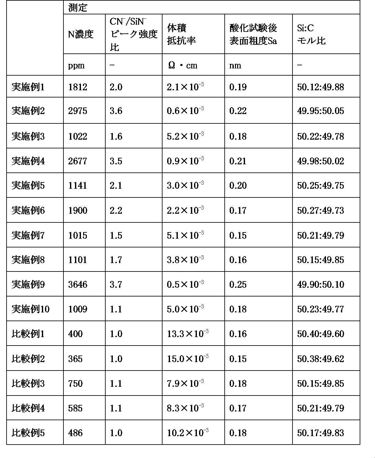
実施例1~10において得られた多結晶SiC成形体の体積抵抗率は、7.0×10⁻³Ω・cm以下である。対照的に、比較例1~5において得られた多結晶SiC成形体の抵抗率は、7.0×10⁻³Ω・cmを超えている。
Claims (4)
- 体積抵抗率が7.0×10⁻³Ω・cm以下であり、
窒素濃度が1000ppmを超えてかつ4500ppm以下の範囲内である、
SiC成形体。 - 飛行時間型二次イオン質量分析法によって測定されるSiN-ピーク強度に対するCN-ピーク強度の比が1.2以上である、請求項1に記載のSiC成形体。
- 前記体積抵抗率が5.0×10⁻³Ω・cm以下である、請求項1又は請求項2に記載のSiC成形体。
- 請求項1に記載のSiC成形体の製造方法であって、
反応室内に、基板を準備することと、
前記反応室内に、ケイ素及び炭素を含む原料ガスと、窒素含有ドーパントガスと、キャリアガスと、塩化水素ガスとを供給して、前記基板の上にSiC膜を形成することと、
前記SiC膜から前記基板を除去することと、を含み、
前記SiC膜を形成する過程における前記反応室内の前記塩化水素ガスの分圧が、1000Pa以上である、
SiC成形体の製造方法。
Priority Applications (5)
| Application Number | Priority Date | Filing Date | Title |
|---|---|---|---|
| EP23897478.6A EP4455360A4 (en) | 2022-12-02 | 2023-11-14 | SIC CAST ARTICLE AND METHOD FOR MANUFACTURING SIC CAST ARTICLE |
| US18/835,005 US20250154647A1 (en) | 2022-12-02 | 2023-11-14 | SiC FORMED BODY AND METHOD FOR PRODUCING SiC FORMED BODY |
| CN202380018557.5A CN118591656A (zh) | 2022-12-02 | 2023-11-14 | SiC成型体及SiC成型体的制造方法 |
| JP2024519815A JP7553750B1 (ja) | 2022-12-02 | 2023-11-14 | SiC成形体及びSiC成形体の製造方法 |
| KR1020247025256A KR20240128986A (ko) | 2022-12-02 | 2023-11-14 | SiC 성형체 및 SiC 성형체의 제조 방법 |
Applications Claiming Priority (2)
| Application Number | Priority Date | Filing Date | Title |
|---|---|---|---|
| JP2022193588 | 2022-12-02 | ||
| JP2022-193588 | 2022-12-02 |
Publications (1)
| Publication Number | Publication Date |
|---|---|
| WO2024116827A1 true WO2024116827A1 (ja) | 2024-06-06 |
Family
ID=91323674
Family Applications (1)
| Application Number | Title | Priority Date | Filing Date |
|---|---|---|---|
| PCT/JP2023/040933 Ceased WO2024116827A1 (ja) | 2022-12-02 | 2023-11-14 | SiC成形体及びSiC成形体の製造方法 |
Country Status (7)
| Country | Link |
|---|---|
| US (1) | US20250154647A1 (ja) |
| EP (1) | EP4455360A4 (ja) |
| JP (1) | JP7553750B1 (ja) |
| KR (1) | KR20240128986A (ja) |
| CN (1) | CN118591656A (ja) |
| TW (1) | TW202436220A (ja) |
| WO (1) | WO2024116827A1 (ja) |
Families Citing this family (2)
| Publication number | Priority date | Publication date | Assignee | Title |
|---|---|---|---|---|
| WO2026071049A1 (ja) * | 2024-09-30 | 2026-04-02 | 東海カーボン株式会社 | 多結晶炭化珪素成形体およびその製造方法 |
| WO2026071050A1 (ja) * | 2024-09-30 | 2026-04-02 | 東海カーボン株式会社 | 多結晶炭化珪素成形体およびその製造方法 |
Citations (4)
| Publication number | Priority date | Publication date | Assignee | Title |
|---|---|---|---|---|
| JP2001220237A (ja) | 2000-02-14 | 2001-08-14 | Asahi Glass Co Ltd | 炭化ケイ素体およびその製造方法 |
| JP2007513257A (ja) * | 2003-12-05 | 2007-05-24 | モーガン・アドヴァンスド・セラミックス・インコーポレイテッド | 化学蒸着によって形成される自立型炭化ケイ素製品及びそれらを製造するための方法 |
| JP2021054667A (ja) | 2019-09-27 | 2021-04-08 | 東海カーボン株式会社 | 多結晶SiC成形体 |
| JP2021054666A (ja) * | 2019-09-27 | 2021-04-08 | 東海カーボン株式会社 | 多結晶SiC成形体及びその製造方法 |
Family Cites Families (3)
| Publication number | Priority date | Publication date | Assignee | Title |
|---|---|---|---|---|
| US6811761B2 (en) * | 2000-11-10 | 2004-11-02 | Shipley Company, L.L.C. | Silicon carbide with high thermal conductivity |
| KR101178234B1 (ko) * | 2010-07-14 | 2012-08-30 | 서울시립대학교 산학협력단 | 이트륨나이트레이트 및 그 화합물 중 적어도 어느 하나를 포함하는 탄화규소 세라믹스 제조용 조성물, 탄화규소 세라믹스 및 그 제조방법 |
| WO2014027472A1 (ja) * | 2012-08-17 | 2014-02-20 | 株式会社Ihi | 耐熱複合材料の製造方法及び製造装置 |
-
2023
- 2023-11-14 JP JP2024519815A patent/JP7553750B1/ja active Active
- 2023-11-14 EP EP23897478.6A patent/EP4455360A4/en active Pending
- 2023-11-14 CN CN202380018557.5A patent/CN118591656A/zh active Pending
- 2023-11-14 WO PCT/JP2023/040933 patent/WO2024116827A1/ja not_active Ceased
- 2023-11-14 KR KR1020247025256A patent/KR20240128986A/ko active Pending
- 2023-11-14 US US18/835,005 patent/US20250154647A1/en active Pending
- 2023-11-30 TW TW112146524A patent/TW202436220A/zh unknown
Patent Citations (4)
| Publication number | Priority date | Publication date | Assignee | Title |
|---|---|---|---|---|
| JP2001220237A (ja) | 2000-02-14 | 2001-08-14 | Asahi Glass Co Ltd | 炭化ケイ素体およびその製造方法 |
| JP2007513257A (ja) * | 2003-12-05 | 2007-05-24 | モーガン・アドヴァンスド・セラミックス・インコーポレイテッド | 化学蒸着によって形成される自立型炭化ケイ素製品及びそれらを製造するための方法 |
| JP2021054667A (ja) | 2019-09-27 | 2021-04-08 | 東海カーボン株式会社 | 多結晶SiC成形体 |
| JP2021054666A (ja) * | 2019-09-27 | 2021-04-08 | 東海カーボン株式会社 | 多結晶SiC成形体及びその製造方法 |
Non-Patent Citations (1)
| Title |
|---|
| See also references of EP4455360A4 |
Also Published As
| Publication number | Publication date |
|---|---|
| KR20240128986A (ko) | 2024-08-27 |
| US20250154647A1 (en) | 2025-05-15 |
| EP4455360A1 (en) | 2024-10-30 |
| TW202436220A (zh) | 2024-09-16 |
| EP4455360A4 (en) | 2026-01-07 |
| CN118591656A (zh) | 2024-09-03 |
| JP7553750B1 (ja) | 2024-09-18 |
| JPWO2024116827A1 (ja) | 2024-06-06 |
Similar Documents
| Publication | Publication Date | Title |
|---|---|---|
| TWI541375B (zh) | SiC成形體及SiC成形體之製造方法 | |
| JP7553750B1 (ja) | SiC成形体及びSiC成形体の製造方法 | |
| CN117401979B (zh) | 一种制备碳化硅陶瓷材料的方法、应用及碳化硅陶瓷材料 | |
| CN118064864A (zh) | 一种制备碳化硅材料的方法、应用及碳化硅材料 | |
| JP2002047066A (ja) | SiC成形体およびその製造方法 | |
| JP7427848B1 (ja) | 多結晶SiC成形体及びその製造方法 | |
| JP2005310861A (ja) | 炭化窒化珪素膜の形成方法 | |
| WO2024058044A1 (ja) | 炭化珪素エピタキシャル基板、エピタキシャル基板の製造方法および炭化珪素半導体装置の製造方法 | |
| JP2019112288A (ja) | 炭化ケイ素部材および半導体製造装置用部材 | |
| JP2019147984A (ja) | 炭化ケイ素部材 | |
| WO2023008439A1 (ja) | 半導体製造装置用の部材およびそのような部材を製造する方法 | |
| JP7550323B1 (ja) | 多結晶SiC成形体及びその製造方法 | |
| JP7669598B1 (ja) | 多結晶SiC成形体 | |
| KR102780851B1 (ko) | 포커스 링 및 그 제조 방법 | |
| JP2021046336A (ja) | 黒鉛製支持基板の表面処理方法、炭化珪素多結晶膜の成膜方法および炭化珪素多結晶基板の製造方法 | |
| WO2024257580A1 (ja) | 炭化珪素エピタキシャル基板、炭化珪素半導体装置の製造方法および炭化珪素エピタキシャル基板の製造方法 | |
| CN120866797A (zh) | 一种制备碳化硅涂层石墨基座的方法及碳化硅涂层石墨基座 | |
| KR20150123075A (ko) | 실리콘 카바이드 성형체 및 그 제조 방법 | |
| JP2024140407A (ja) | 多結晶SiC自立成形体 | |
| JP2006152338A (ja) | ダイヤモンド被覆電極及びその製造方法 |
Legal Events
| Date | Code | Title | Description |
|---|---|---|---|
| WWE | Wipo information: entry into national phase |
Ref document number: 2024519815 Country of ref document: JP |
|
| 121 | Ep: the epo has been informed by wipo that ep was designated in this application |
Ref document number: 23897478 Country of ref document: EP Kind code of ref document: A1 |
|
| WWE | Wipo information: entry into national phase |
Ref document number: 202380018557.5 Country of ref document: CN |
|
| ENP | Entry into the national phase |
Ref document number: 20247025256 Country of ref document: KR Kind code of ref document: A |
|
| ENP | Entry into the national phase |
Ref document number: 2023897478 Country of ref document: EP Effective date: 20240724 |
|
| WWE | Wipo information: entry into national phase |
Ref document number: 18835005 Country of ref document: US |
|
| WWP | Wipo information: published in national office |
Ref document number: 18835005 Country of ref document: US |
|
| NENP | Non-entry into the national phase |
Ref country code: DE |