WO2024214322A1 - Dispositif de conversion de puissance - Google Patents
Dispositif de conversion de puissance Download PDFInfo
- Publication number
- WO2024214322A1 WO2024214322A1 PCT/JP2023/037628 JP2023037628W WO2024214322A1 WO 2024214322 A1 WO2024214322 A1 WO 2024214322A1 JP 2023037628 W JP2023037628 W JP 2023037628W WO 2024214322 A1 WO2024214322 A1 WO 2024214322A1
- Authority
- WO
- WIPO (PCT)
- Prior art keywords
- conversion device
- power conversion
- current
- switching
- regeneration
- Prior art date
- Legal status (The legal status is an assumption and is not a legal conclusion. Google has not performed a legal analysis and makes no representation as to the accuracy of the status listed.)
- Ceased
Links
Images

Classifications
-
- H—ELECTRICITY
- H02—GENERATION; CONVERSION OR DISTRIBUTION OF ELECTRIC POWER
- H02M—APPARATUS FOR CONVERSION BETWEEN AC AND AC, BETWEEN AC AND DC, OR BETWEEN DC AND DC, AND FOR USE WITH MAINS OR SIMILAR POWER SUPPLY SYSTEMS; CONVERSION OF DC OR AC INPUT POWER INTO SURGE OUTPUT POWER; CONTROL OR REGULATION THEREOF
- H02M7/00—Conversion of AC power input into DC power output; Conversion of DC power input into AC power output
- H02M7/42—Conversion of DC power input into AC power output without possibility of reversal
- H02M7/44—Conversion of DC power input into AC power output without possibility of reversal by static converters
- H02M7/48—Conversion of DC power input into AC power output without possibility of reversal by static converters using discharge tubes with control electrode or semiconductor devices with control electrode
-
- H—ELECTRICITY
- H02—GENERATION; CONVERSION OR DISTRIBUTION OF ELECTRIC POWER
- H02P—CONTROL OR REGULATION OF ELECTRIC MOTORS, ELECTRIC GENERATORS OR DYNAMO-ELECTRIC CONVERTERS; CONTROLLING TRANSFORMERS, REACTORS OR CHOKE COILS
- H02P27/00—Arrangements or methods for the control of AC motors characterised by the kind of supply voltage
- H02P27/04—Arrangements or methods for the control of AC motors characterised by the kind of supply voltage using variable-frequency supply voltage, e.g. inverter or converter supply voltage
- H02P27/06—Arrangements or methods for the control of AC motors characterised by the kind of supply voltage using variable-frequency supply voltage, e.g. inverter or converter supply voltage using DC to AC converters or inverters
Definitions
- the present invention relates to a power conversion device that supplies AC power to a motor.
- a power conversion device for driving a motor generally consists of a rectifier section that converts AC voltage to DC voltage, a smoothing capacitor that smoothes the DC voltage, and an inverter section that reverse converts the DC voltage.
- the inverter section generally consists of a three-phase bridge using six switching elements, and by switching these switching elements in a pattern generated based on a pulse width modulation (PWM) method or the like, it is possible to output three-phase AC power with any voltage and frequency.
- PWM pulse width modulation
- a method in which a current detection resistor is placed between the low-voltage side of the DC voltage and the lower-arm switching element of the inverter section, and the current value is detected from the voltage across the current detection resistor, in order to control the switching elements and protect them from overcurrent.
- This method is easy to implement because it can be constructed using small components, but due to its operating principle, the current flowing through the upper-arm switching element cannot be directly detected by the current detection resistor, so an overcurrent protection circuit must be configured to protect the upper-arm switching element from overcurrent.
- Regenerative operation is a typical example of an overcurrent occurring in the upper arm switching element.
- the current flowing from the motor to the inverter increases if the induced voltage of the motor is short-circuited via the three-phase bridge.
- the configuration must be such that the current does not rise to the withstand current value of the switching element.
- Patent Document 1 is a related technique in this technical field.
- Patent Document 1 describes a power conversion device that, in an inverter section configured with a three-phase bridge, causes the lower arm switching elements of the three-phase bridge to return current when the DC voltage rises to a predetermined value.
- Patent Document 1 Figures 1, 2, and 3, and paragraphs [0010], [0024], and [0030], describe a power conversion device that, for a three-phase bridge configured with a resistor between the lower-arm switching element and the low-voltage side of the DC voltage and capable of detecting overcurrent with the resistive element, causes the lower-arm switching element of the three-phase bridge to flow back when the DC voltage exceeds a predetermined value due to regenerative operation caused by sudden motor deceleration or other reasons.
- This allows the regenerative energy to be absorbed as thermal energy by the resistive element, eliminating the need for a large regenerative resistor or regenerative switch.
- the DC voltage rise and the current resistance characteristics of the inverter are essentially separate characteristics.
- a power conversion device in which a large-capacity electrolytic capacitor is mounted as a smoothing capacitor and the inverter section switches based on the PWM method
- the DC voltage barely rises immediately after the motor starts to decelerate the period from t1 to t2 in Figures 2 and 3 of Patent Document 1
- the current flowing through the upper arm switching element increases due to the induced voltage of the motor.
- the object of the present invention is to provide a power conversion device that is capable of continuous regenerative operation while preventing the inverter's switching elements from being damaged by overcurrent and the switching elements from becoming too large.
- the present invention is configured as follows:
- the power conversion device includes a rectifier that converts AC voltage to DC voltage, an inverter that converts the DC voltage to AC voltage and supplies power to a motor, a control unit that controls the switching elements of the inverter unit, a current detection resistor that is connected to the low-voltage side of the DC voltage and the lower-arm switching element of the inverter unit and detects the current flowing through the lower-arm switching element, and an overcurrent detection unit that calculates the maximum current value flowing through the inverter unit based on the current flowing through the current detection resistor and outputs an overcurrent detection signal when the maximum current value exceeds at least a first current level, and the control unit controls the switching elements so that a period is included in which the switching frequency of the inverter unit during regeneration is higher than the switching frequency during power running.
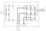
- FIG. 1 is a circuit configuration diagram of a power conversion device according to a first embodiment.
- 13 is an example of a case where the present invention is not applied, and shows operational waveforms for explaining the principle of an overcurrent occurring in an upper arm switching element.
- 4 shows operational waveforms of the power conversion device in the first embodiment.
- 11 is an operational waveform showing a modified example of the operation of the first embodiment.
- 10 is an operational waveform illustrating the principle by which an overcurrent occurs in an upper arm switching element in the second embodiment.
- 13 shows operational waveforms of the power conversion device in the third embodiment.
- FIG. 11 is a circuit configuration diagram of a power conversion device according to a fourth embodiment.
- Fig. 1 is a configuration diagram of a power conversion device 1 in the present embodiment 1.
- the power conversion device 1 includes a rectifier unit 2 that inputs an AC voltage and outputs a DC voltage, a smoothing capacitor 3 that smoothes the DC voltage, an inverter unit 4 configured with a three-phase bridge that converts the DC voltage into AC power, a current detection unit 5 arranged between lower arm switching elements 42, 44, 46 of the inverter unit 4 and the low voltage side of the DC voltage, an overcurrent detection unit 6 that outputs an overcurrent detection signal when a current flowing through the inverter unit 4 exceeds a judgment value (first current level) based on a current value detected by the current detection unit 5, and a control unit 7 that outputs a drive signal to the switching elements of the inverter unit 4.
- a rectifier unit 2 that inputs an AC voltage and outputs a DC voltage
- a smoothing capacitor 3 that smoothes the DC voltage
- an inverter unit 4 configured with a three-phase bridge that converts the DC
- the rectifier unit 2 is composed of multiple diodes, and converts the AC voltage input from the input terminal into a DC voltage, which is output to both electrodes of the smoothing capacitor 3.
- the rectification action of the diodes in the rectifier unit 2 generates a DC voltage with a positive voltage on the DC voltage wiring on the node P side and a negative voltage on the DC voltage wiring on the node N side.
- the smoothing capacitor 3 is connected to the DC voltage wiring at nodes P and N and smoothes the DC voltage.
- Figure 1 shows a representative example of a method for full-wave rectifying single-phase AC, it may also be configured with a method for full-wave rectifying three-phase AC, a method for voltage-doubler rectifying single-phase AC, or a regenerative converter that can exchange power in both directions between AC and DC.
- the inverter section 4 is composed of switching elements 41 to 46.
- the switching elements 41 to 46 operate to charge the smoothing capacitor 3 with regenerative energy from the motor 9.
- switching elements 41 to 46 shown in FIG. 1 use the circuit symbol IGBT as a representative example, but it is also possible to use other power semiconductors such as MOSFETs.
- the current detection unit 5 is composed of current detection resistors 51-53, which are respectively arranged between the emitter terminals of the lower arm switching elements 42, 44, 46 of the inverter unit 4 and the low voltage side of the DC voltage.
- the current detection resistors 51-53 detect the voltage across the current detection resistors 51, 52, 53 in the switching pattern of the inverter unit 4 where current flows through the switching elements 42, 44, 46, making it possible to partially detect the current flowing through the motor 9.
- FIG. 2 is an example of operational control when the present invention is not applied, and shows operational waveforms of each part of the power conversion device 1 when an overcurrent occurs in the upper arm switching element 41 in FIG. 1.
- IU, IV, and IW are the currents flowing through the U-phase, V-phase, and W-phase motors, respectively, with the positive direction flowing out from the inverter unit 4 to the motor 9 and the negative direction flowing in from the motor 9 to the inverter unit 4.
- IU is shown by a solid line, IV by a dashed line, and IW by a dashed line.
- Ith1 is the overcurrent level, and is a value that is set with a margin for the allowable current of the switching elements and motor.
- VU-N, VV-N, VW-N are the potential differences between the U, V, and W phases and node N, which is the low-voltage side of the DC voltage; ignoring the conduction voltage drop of the switching elements, this is roughly the DC voltage value when the upper arm switching element is conducting, and roughly 0V when the lower arm switching element is conducting.
- VU-N is shown by a solid line, VV-N by a dashed line, and VW-N by a dashed line.
- the overcurrent detection signal is configured to output H if the current value of the switching element through which the most current is flowing, calculated from the current values detected by current detection resistors 51, 52, and 53, is below overcurrent level Ith1, and output L if it is above it.
- Figure 2 shows the waveforms when the motor suddenly decelerates from a mode in which it was powered by two-phase modulation due to a DC braking command input at time t1, switches to regeneration mode, and at time t5 a current exceeding the overcurrent level Ith1 flows through the U-phase current detection resistor, causing switching elements 41 to 46 to stop in the off state.
- the period marked “below the freewheel arm” indicates an operating mode in which the main circuit current flows back between switching elements 42, 44, and 46 on the lower arm side of inverter unit 4 during regeneration.
- the period marked “above the freewheel arm” indicates an operating mode in which the main circuit current flows back between switching elements 41, 43, and 45 on the upper arm side of inverter unit 4 during regeneration.
- the two-phase modulation method is a method for PWM control of a three-phase inverter in which one phase is fixed to 1 or 0 during a specific section of one cycle of a modulated wave, and the other two phases are modulated.
- FIG. 2 it can be seen that before time t1, the upper arm switching element 43 of the V phase is in the on state, and the lower arm switching element 44 is in the off state.
- DC braking is an operation in which a DC voltage is applied to the motor 9 to reliably stop the motor, and the inverter unit 4 outputs approximately 0 Hz. Therefore, after t1 when DC braking starts, the upper arm reflux period (t2 to t3, t4 to t5) or the lower arm reflux period (t1 to t2, t3 to t4, t5 to t6) becomes dominant.
- FIG. 3 shows the operating waveforms of each part of the power conversion device 1 when the operation control in this embodiment 1 is applied.
- the power conversion device 1 in this embodiment 1 is characterized in that the switching frequency is made higher than that during power running at time t1 when the DC braking command is input.
- the upper arm return period from t10 to t11 shown in FIG. 3 is shorter than the upper arm return period from t4 to t5 shown in FIG. 2, so that the amount of excess current exceeding the overcurrent level Ith1 during the upper arm return period is reduced.
- the excess current B shown in FIG. 3 is smaller than the excess current A shown in FIG. 2, making it possible to suppress the destruction of the upper arm switching elements due to the overcurrent.
- the excess current A does not satisfy the withstand current value of the switching elements 41 to 46, it is necessary to apply a large switching element with a high withstand current value, so by reducing the excess current, it is possible to prevent the switching elements from becoming large.
- the increase in the switching frequency can be achieved by increasing the frequency of the carrier wave (carrier frequency) that is compared with the modulated wave in PWM control. That is, the control unit 7 starts processing to increase the carrier frequency when a command is input, and after this processing is completed, the control unit 7 increases the switching frequency of the drive signal output from the control unit 7. Also, when the command is released and the motor enters a powering state, the control unit 7 starts processing to again decrease the carrier frequency, and after this processing is completed, the control unit 7 decreases the switching frequency of the drive signal output from the control unit 7.
- the excess current value from overcurrent level Ith1 is reduced below excess current B shown in FIG. 3, and if overcurrent level Ith1 is set to the same value as in FIG. 3, the margin for the withstand current value of switching elements 41 to 46 increases. In other words, even if the overcurrent level value is increased by the amount by which the excess current value is reduced from excess current B shown in FIG. 3, the withstand current value of switching elements 41 to 46 is satisfied. In this way, by adjusting the value of the overcurrent level according to the value of the switching frequency during regenerative operation, it is possible to obtain an appropriate current value and regenerative braking force.
- FIG. 4 shows an example of operation after an overcurrent is detected and stopped in FIG. 3. As shown in FIG. 4, after stopping, if the U-phase current IU, V-phase current IV, and W-phase current IW all fall below the overcurrent level Ith1 and the overcurrent detection signal transitions from L to H, inverter unit 4 is no longer in an overcurrent state and switching can be resumed.
- the overcurrent detection unit 6 detects an overcurrent, transitions the overcurrent detection signal from H to L, and the control unit 7 stops the switching elements 41 to 46 in the OFF state. Thereafter, as the switching stops, the current flowing through the inverter unit 4 gradually approaches zero, and at time t2 in FIG. 4, the current flowing through the inverter unit 4 falls below the overcurrent level Ith1, and the overcurrent detection signal transitions from H to L.
- the power conversion device 1 includes a period during which the switching frequency in the inverter unit 4 having a three-phase bridge is made higher during regeneration than during power running. This makes it possible to prevent damage to the upper arm switching elements 41, 43, and 45 due to overcurrent even if the overcurrent level is set to a high value.
- the control unit 7 can estimate whether the operation is powering or regenerative from, for example, the modulation factor generated by the motor drive control of the control unit 7. If the operation is powering, the modulation factor will be a positive value, and if the operation is regenerative, the modulation factor will be a negative value. In this way, by switching the switching frequency with reference to the value inside the control unit 7, it is possible to realize the operation shown in this embodiment with a simple configuration.
- the first embodiment it is possible to provide a power conversion device 1 capable of continuous regenerative operation while preventing the switching elements 41 to 46 of the inverter unit 4 from being destroyed by an overcurrent and preventing the switching elements 41 to 46 from becoming large.
- Example 1 regeneration refers to DC braking operation when stopped.
- the period during which the switching frequency during regeneration is higher than the switching frequency during power running does not have to be the entire period during regeneration, but only needs to include the period during which the switching frequency during regeneration in the inverter unit 4 is controlled to be higher than the switching frequency during power running.
- the switching frequency during regeneration can be set to a value between 0.1 kHz higher than the switching frequency during power running and the upper limit of audible frequencies.
- the second embodiment is an example in which, regarding a regenerative operation different from the regenerative operation described in the first embodiment, the effect of increasing the switching frequency during regenerative operation compared to during power running can be obtained.
- FIG. 5 shows the operating waveforms of each part of the power conversion device 1 when an overcurrent occurs in the upper arm switching element 45 in FIG. 1.
- the two-phase modulation method is used both during power running and regeneration, and before time t1 in FIG. 5, the lower arm switching element 42 of the U phase is on, and after time t1, the upper arm switching element 45 of the W phase is on.
- FIG. 5 shows the operating waveforms after transitioning to regenerative operation, and is in the middle of deceleration according to the set deceleration time.
- the periods from time t1 to t2, t3 to t4, t5 to t6, and t7 to t8 are periods during which all upper arm switching elements 41, 43, and 45 are conductive and all lower arm switching elements 42, 44, and 46 are off, or periods during which the upper arm switching elements for two phases of the three-phase bridge are conductive and the lower arm switching element for one phase is conductive.
- the two-phase modulation method has the problem that it is difficult to detect overcurrent in the upper arm switching elements 41, 43, and 45 during the period when the upper arm switching elements 41, 43, and 45 are in the on state. Therefore, it is also effective to switch from the two-phase modulation method to the three-phase modulation method during regenerative operation.
- the switching frequency is increased or switched to the three-phase modulation method, making it possible to suppress overcurrent in the upper arm switching elements 41, 43, 45.
- the deceleration and stopping operation as in the first embodiment, it is possible to provide a power conversion device capable of continuous regenerative operation while preventing damage to the switching elements of the inverter unit and the increase in size of the switching elements due to overcurrent. Also, in the operation described in this embodiment 2, it is possible to apply the continuous regenerative operation described in FIG. 4 after overcurrent detection.
- Example 3 Next, a description will be given of Example 3.
- the power conversion device 1 of Example 3 sets a switching frequency switching level Ith2 (second current level) lower than the overcurrent level Ith1, and increases the switching frequency when the maximum current value calculated based on the current values detected by the current detection resistors 51, 52, and 53 exceeds the switching frequency switching level Ith2.
- Ith2 second current level
- Figure 6 shows the waveforms when the motor 9 suddenly decelerates from a mode in which it was powered using two-phase modulation due to a DC braking command input at time t1, and at time t7 a current exceeding the overcurrent level Ith1 flows through the U-phase current detection resistor, causing the switching elements 41 to 46 to stop in the off state.
- the power conversion device 1 described in this embodiment 3 controls the switching frequency to be the same as during power running (before t1 in Figure 6) when the maximum current value calculated during regeneration falls below the switching frequency switching level Ith2 (t1 to t4 in Figure 6), and controls the switching frequency to be higher than during power running (before t1 in Figure 6) when the maximum current value exceeds Ith2 (t4 to t7 in Figure 6).
- the switching frequency changeover level Ith2 is set as a value with a predetermined margin with respect to the overcurrent level Ith1, and the switching frequency is increased only when the calculated current value exceeds Ith2.
- the third embodiment it is possible to obtain the same effect as the first embodiment, and also to simplify the cooling performance of the inverter section 4.
- FIG. 7 is a configuration diagram of the power conversion device 1 in this embodiment 4.
- a regeneration command unit 8 is added to the power conversion device 1 shown in FIG. 1.
- the switching frequency was increased by using a DC braking command as a trigger
- the switching frequency was increased by using a regeneration command as a trigger, but in the power conversion device described in this embodiment, the command is given from the regeneration command unit 8 to the control unit 7.
- Example 4 shows a modified example.
- the regeneration command unit 8 can receive commands, for example, from a field bus such as a PLC (programmable logic controller) connected to an external input terminal, or from an operator via an external operation panel. In this way, the control unit 7 controls the power conversion device 1 to increase the switching frequency when a DC braking command or a deceleration/stop command is input from outside.
- a field bus such as a PLC (programmable logic controller) connected to an external input terminal
- the control unit 7 controls the power conversion device 1 to increase the switching frequency when a DC braking command or a deceleration/stop command is input from outside.
- Example 4 can also improve the reliability of the operation of the power conversion device 1, as described above.
- Example 4 the configuration can be configured to perform the same operations as any of Examples 1 to 3.
Landscapes
- Engineering & Computer Science (AREA)
- Power Engineering (AREA)
- Inverter Devices (AREA)
Abstract
La présente invention concerne un dispositif de conversion de puissance qui permet d'effectuer une opération de régénération continue tout en empêchant la destruction d'un élément de commutation d'une unité d'onduleur en raison d'une surintensité et une augmentation de la taille de l'élément de commutation. Un dispositif de conversion de puissance 1 comprend : une unité de redressement 2 pour convertir une tension alternative en tension continue ; une unité d'inversion 4 pour convertir la tension continue en tension alternative et alimenter un moteur 9 ; une unité de commande 7 pour commuter les éléments 41-46 de l'unité d'inversion 4 ; des résistances de détection de courant 51, 52, 53 qui sont connectées au côté basse tension de la tension continue et aux éléments de commutation 42, 44, 46 côté bras inférieur de l'unité d'inversion 4 pour détecter les courants dans les éléments de commutation 42, 44, 46 côté bras inférieur ; et une unité de détection de surintensité 6 pour calculer la valeur de courant maximale de l'unité d'onduleur 4 sur la base des courants dans les résistances de détection de courant 51, 52, 53, et émettre un signal de détection de surintensité lorsqu'un premier niveau de courant Ith1 est dépassé. L'unité de commande 7 pilote les éléments de commutation pendant une période au cours de laquelle la fréquence de commutation de l'unité d'onduleur 4 pendant la régénération est supérieure à une fréquence de commutation pendant le fonctionnement.
Applications Claiming Priority (2)
| Application Number | Priority Date | Filing Date | Title |
|---|---|---|---|
| JP2023-065551 | 2023-04-13 | ||
| JP2023065551A JP2024151825A (ja) | 2023-04-13 | 2023-04-13 | 電力変換装置 |
Publications (1)
| Publication Number | Publication Date |
|---|---|
| WO2024214322A1 true WO2024214322A1 (fr) | 2024-10-17 |
Family
ID=93059294
Family Applications (1)
| Application Number | Title | Priority Date | Filing Date |
|---|---|---|---|
| PCT/JP2023/037628 Ceased WO2024214322A1 (fr) | 2023-04-13 | 2023-10-18 | Dispositif de conversion de puissance |
Country Status (2)
| Country | Link |
|---|---|
| JP (1) | JP2024151825A (fr) |
| WO (1) | WO2024214322A1 (fr) |
Citations (11)
| Publication number | Priority date | Publication date | Assignee | Title |
|---|---|---|---|---|
| JPH11316249A (ja) * | 1998-04-30 | 1999-11-16 | Toshiba Corp | 電流検出回路および過電流保護回路 |
| JP2001352790A (ja) * | 2000-06-07 | 2001-12-21 | Mitsubishi Electric Corp | 電動機駆動用制御装置 |
| JP2002374689A (ja) * | 2001-06-14 | 2002-12-26 | Mitsubishi Electric Corp | 電動機駆動装置及び洗濯機 |
| JP2003319699A (ja) * | 2002-04-24 | 2003-11-07 | Toyoda Mach Works Ltd | 電動パワーステアリング装置 |
| JP2005269808A (ja) * | 2004-03-19 | 2005-09-29 | Renesas Technology Corp | モータ駆動回路とモータ駆動制御回路 |
| JP2007110779A (ja) * | 2005-10-11 | 2007-04-26 | Matsushita Electric Ind Co Ltd | モータ駆動装置および駆動方法 |
| JP2009303338A (ja) * | 2008-06-11 | 2009-12-24 | Nec Electronics Corp | モータ駆動装置と制御方法 |
| JP2010028894A (ja) * | 2008-07-15 | 2010-02-04 | Nec Electronics Corp | モータ駆動装置と制御方法 |
| JP2013231601A (ja) * | 2012-04-27 | 2013-11-14 | Mitsubishi Electric Corp | 電力変換装置の電流検出装置、およびこの電流検出装置を備えた半導体モジュール |
| WO2021065761A1 (fr) * | 2019-10-01 | 2021-04-08 | 株式会社デンソー | Dispositif de commande de machine électrique tournante |
| US20220200440A1 (en) * | 2019-04-11 | 2022-06-23 | Ls Electric Co., Ltd. | Overcurrent protection inverter |
-
2023
- 2023-04-13 JP JP2023065551A patent/JP2024151825A/ja active Pending
- 2023-10-18 WO PCT/JP2023/037628 patent/WO2024214322A1/fr not_active Ceased
Patent Citations (11)
| Publication number | Priority date | Publication date | Assignee | Title |
|---|---|---|---|---|
| JPH11316249A (ja) * | 1998-04-30 | 1999-11-16 | Toshiba Corp | 電流検出回路および過電流保護回路 |
| JP2001352790A (ja) * | 2000-06-07 | 2001-12-21 | Mitsubishi Electric Corp | 電動機駆動用制御装置 |
| JP2002374689A (ja) * | 2001-06-14 | 2002-12-26 | Mitsubishi Electric Corp | 電動機駆動装置及び洗濯機 |
| JP2003319699A (ja) * | 2002-04-24 | 2003-11-07 | Toyoda Mach Works Ltd | 電動パワーステアリング装置 |
| JP2005269808A (ja) * | 2004-03-19 | 2005-09-29 | Renesas Technology Corp | モータ駆動回路とモータ駆動制御回路 |
| JP2007110779A (ja) * | 2005-10-11 | 2007-04-26 | Matsushita Electric Ind Co Ltd | モータ駆動装置および駆動方法 |
| JP2009303338A (ja) * | 2008-06-11 | 2009-12-24 | Nec Electronics Corp | モータ駆動装置と制御方法 |
| JP2010028894A (ja) * | 2008-07-15 | 2010-02-04 | Nec Electronics Corp | モータ駆動装置と制御方法 |
| JP2013231601A (ja) * | 2012-04-27 | 2013-11-14 | Mitsubishi Electric Corp | 電力変換装置の電流検出装置、およびこの電流検出装置を備えた半導体モジュール |
| US20220200440A1 (en) * | 2019-04-11 | 2022-06-23 | Ls Electric Co., Ltd. | Overcurrent protection inverter |
| WO2021065761A1 (fr) * | 2019-10-01 | 2021-04-08 | 株式会社デンソー | Dispositif de commande de machine électrique tournante |
Also Published As
| Publication number | Publication date |
|---|---|
| JP2024151825A (ja) | 2024-10-25 |
Similar Documents
| Publication | Publication Date | Title |
|---|---|---|
| JP6169203B1 (ja) | 電動機制御装置および電動機制御方法 | |
| US8624538B2 (en) | Motor driving apparatus having function of dynamically switching converter operation mode of AC/DC converter | |
| US8283880B2 (en) | Motor drive device with function of switching to power regenerative operation mode | |
| EP2157688A1 (fr) | Dispositif d'entraînement de moteur, dispositif de moteur, et dispositif de circuit intégré | |
| EP2763311A1 (fr) | Dispositif de commande vectorielle pour moteur électrique, moteur électrique, système d'entraînement de véhicule et procédé de commande vectorielle pour moteur électrique | |
| TWI728837B (zh) | 電力轉換裝置及壓製裝置 | |
| JP4479422B2 (ja) | 洗濯機のモータ制御装置 | |
| EP3672066A1 (fr) | Circuit de commande pour outil électrique | |
| WO2024214322A1 (fr) | Dispositif de conversion de puissance | |
| JP2008154431A (ja) | モータ制御装置 | |
| JP6157770B1 (ja) | サーボモータ制御装置 | |
| CN101257279A (zh) | 电动机驱动装置 | |
| JP4449283B2 (ja) | Pwmインバータの制御方法 | |
| JP4552738B2 (ja) | 洗濯機のモータ制御装置 | |
| JP3882496B2 (ja) | インバータ装置 | |
| JP2014161221A (ja) | 電力変換装置 | |
| JP4780305B2 (ja) | インバータ装置 | |
| JPH0127436Y2 (fr) | ||
| JP2005261161A (ja) | モータの駆動制御方法および駆動制御装置 | |
| JP2025026196A (ja) | 電力変換装置 | |
| JP2000253686A (ja) | 電力回生回路 | |
| JP2021083219A (ja) | 回生放電システム | |
| JP3788302B2 (ja) | 誘導機の制御装置 | |
| JPS61150683A (ja) | インバ−タ駆動誘導電動機の直流制動方式 | |
| JPS62230574A (ja) | 交流エレベ−タの制御装置 |
Legal Events
| Date | Code | Title | Description |
|---|---|---|---|
| 121 | Ep: the epo has been informed by wipo that ep was designated in this application |
Ref document number: 23933097 Country of ref document: EP Kind code of ref document: A1 |
|
| NENP | Non-entry into the national phase |
Ref country code: DE |
|
| 122 | Ep: pct application non-entry in european phase |
Ref document number: 23933097 Country of ref document: EP Kind code of ref document: A1 |