WO2024252534A1 - Optical modulator - Google Patents
Optical modulator Download PDFInfo
- Publication number
- WO2024252534A1 WO2024252534A1 PCT/JP2023/021061 JP2023021061W WO2024252534A1 WO 2024252534 A1 WO2024252534 A1 WO 2024252534A1 JP 2023021061 W JP2023021061 W JP 2023021061W WO 2024252534 A1 WO2024252534 A1 WO 2024252534A1
- Authority
- WO
- WIPO (PCT)
- Prior art keywords
- optical waveguide
- type optical
- rib
- type
- width
- Prior art date
- Legal status (The legal status is an assumption and is not a legal conclusion. Google has not performed a legal analysis and makes no representation as to the accuracy of the status listed.)
- Ceased
Links
Images


Classifications
-
- G—PHYSICS
- G02—OPTICS
- G02B—OPTICAL ELEMENTS, SYSTEMS OR APPARATUS
- G02B6/00—Light guides; Structural details of arrangements comprising light guides and other optical elements, e.g. couplings
- G02B6/10—Light guides; Structural details of arrangements comprising light guides and other optical elements, e.g. couplings of the optical waveguide type
- G02B6/12—Light guides; Structural details of arrangements comprising light guides and other optical elements, e.g. couplings of the optical waveguide type of the integrated circuit kind
- G02B6/122—Basic optical elements, e.g. light-guiding paths
- G02B6/125—Bends, branchings or intersections
-
- G—PHYSICS
- G02—OPTICS
- G02F—OPTICAL DEVICES OR ARRANGEMENTS FOR THE CONTROL OF LIGHT BY MODIFICATION OF THE OPTICAL PROPERTIES OF THE MEDIA OF THE ELEMENTS INVOLVED THEREIN; NON-LINEAR OPTICS; FREQUENCY-CHANGING OF LIGHT; OPTICAL LOGIC ELEMENTS; OPTICAL ANALOGUE/DIGITAL CONVERTERS
- G02F1/00—Devices or arrangements for the control of the intensity, colour, phase, polarisation or direction of light arriving from an independent light source, e.g. switching, gating or modulating; Non-linear optics
- G02F1/01—Devices or arrangements for the control of the intensity, colour, phase, polarisation or direction of light arriving from an independent light source, e.g. switching, gating or modulating; Non-linear optics for the control of the intensity, phase, polarisation or colour
Definitions
- This disclosure relates to an optical modulator, and more specifically to an optical modulator using a rib-type optical waveguide.
- multilevel optical modulators using digital coherent technology are playing a major role in realizing high-capacity transceivers that exceed 100 Gbps.
- a multilevel optical modulator splits the input light into two arm optical waveguides, modulates the light propagating through the arm optical waveguides, aligns the phase, and then combines and outputs the resulting interference.
- the multilevel optical modulator has multiple parallel-stage built-in optical modulators (hereafter referred to as MZ modulators: MZMs) capable of zero-chirp drive. This configuration allows independent signals to be added to the amplitude and phase of the light.
- Typical polarization multiplexing IQ optical modulators which are currently being used in communication networks, have a so-called nested structure, in which each arm of a parent MZM is composed of a child MZM.
- Two child MZMs are provided in parallel corresponding to each of the X and Y polarization channels, forming an MZM (Quad-parallel MZM) with a total of four child MZMs.
- the two arms of each child MZM are provided with traveling wave type electrodes to which an RF modulated electrical signal is input to perform a modulation operation on the optical signal propagating in the optical waveguide.
- one of the two such paired child MZMs corresponds to the I channel and the other to the Q channel.
- Such a polarization multiplexed IQ optical modulator applies phase modulation to two optical signals propagating within the optical waveguide of the child MZM by inputting an RF modulated electrical signal to one end of a modulation electrode provided along the arm optical waveguide of the child MZM, thereby generating an electro-optic effect (see, for example, Patent Document 1).
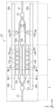
- FIG. 1 shows an example of a high-speed phase modulator using a Mach-Zehnder interferometer, which corresponds to the child MZM that is the basic unit in a polarization multiplexing IQ optical modulator.
- a Mach-Zehnder interferometer which corresponds to the child MZM that is the basic unit in a polarization multiplexing IQ optical modulator.
- the high-mesa type optical waveguides 113a and 113b are connected to rib type optical waveguides 114a and 114b, respectively.
- the rib type optical waveguides 114a and 114b are connected to high-mesa type optical waveguides 115a and 115b, respectively.
- the two rib type optical waveguides 114a and 114b are separated by a separation groove 118.
- the high mesa optical waveguides 115a and 115b are connected to a 2x1 multiplexer 116 having a high mesa optical waveguide structure.
- the 2x1 multiplexer 116 is connected to one high mesa optical waveguide 117.
- the high mesa type optical waveguides 113a, 113b, the rib type optical waveguides 114a, 114b, and the high mesa type optical waveguides 115a, 115b form an arm optical waveguide that connects the 1x2 demultiplexer 112 and the 2x1 multiplexer 116.
- two high-frequency lines 120a, 120b extending in the light propagation direction (x direction) are formed along the arm optical waveguide. The ends of the high-frequency lines 120a, 120b are connected to termination resistors 150a, 150b.
- a plurality of slot electrodes 121a, 121b are formed discretely above the rib type optical waveguides 114a, 114b, respectively, and function as an optical modulator that adds a signal to light by the electro-optic effect.
- the multiple slot electrodes 121a, 121b are connected to the two high-frequency lines 120a, 120b by multiple connection electrodes 122a, 122b, respectively.
- the high mesa optical waveguides 115a, 115b are respectively loaded with thin-film heaters 130a, 130b on the upper side, and function as thermo-optical phase shifters.
- the thin-film heaters 130a, 130b are respectively connected to the two pads 131a, 131b by wiring 132a, 132b.
- the high-speed phase modulator 100 can be divided into a high-mesa optical waveguide region A including a high-mesa optical waveguide 111, a 1 ⁇ 2 splitter 112, and high-mesa optical waveguides 113a and 113b, a high-speed modulation region and rib-type optical waveguide region B including rib-type optical waveguides 114a and 114b, and a high-mesa optical waveguide region C including high-mesa optical waveguides 151 and 115b, a 2 ⁇ 1 multiplexer 116, and a high-mesa optical waveguide 117.
- each optical waveguide has a tapered shape to suppress optical connection loss.
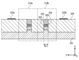
- FIG. 2 shows a cross section taken along line II-II in Figure 1.
- the high mesa optical waveguides 113a and 113b will be described with reference to Figure 2.
- the high mesa optical waveguides 113a and 113b have a structure in which an n-type InP lower cladding layer 202, a p-type InP layer 203, an i-type MQW (Multi Quantum Well) core layer 204, and a high resistance (or non-doped) InP upper cladding layer 205 are stacked on a semi-insulating InP substrate 201.
- the high resistance InP upper cladding layer 205 is formed by etching the n-type InP upper cladding layer and replacing it by regrowth.
- the width W113 of the high-resistance InP upper cladding layer 205 and the i-type MQW core layer 204 in the lateral direction (y direction) perpendicular to the light propagation direction is uniform and is several ⁇ m wide (for example, 2 ⁇ m wide).
- the lateral direction (y direction) of the high mesa optical waveguides 113a and 113b is covered with an organic film (BCB: benzocyclobutene) 206, and the large refractive index difference between the i-type MQW core layer 204 and the organic film 206 realizes lateral light confinement.
- BCB benzocyclobutene
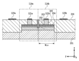
- Figure 3 shows a cross section taken along line III-III in Figure 1.
- the rib type optical waveguides 114a and 114b will be described with reference to Figure 3.
- the InP semiconductor layer structure of the rib type optical waveguides 114a and 114b is similar to that of the high mesa type optical waveguides 113a and 113b described with reference to Figure 2, but the upper cladding layer is different.
- the upper cladding layer of the high mesa type optical waveguides 113a and 113b in Figure 2 is a high resistance (or non-doped) InP upper cladding layer 205
- the upper cladding layer of the rib type optical waveguides 114a and 114b in Figure 3 is an n-type InP upper cladding layer 305, which is different.
- electrical contact is obtained by using an n-type InP upper cladding layer 305 as the upper cladding layer, making it possible to apply an electric field to the i-type MQW core layer 204.
- the width (y direction) of the n-type InP upper cladding layer 305 in the lateral direction (y direction) is narrower than the slab width W114 of the i-type MQW core layer 204, the p-type InP layer 203, and the n-type InP lower cladding layer 202.
- the slab width W114 is uniform.
- the rib-type optical waveguides 114a and 114b confine light by a lateral confinement effect equivalent to the width of the n-type InP upper cladding layer 305.
- the rib-type optical waveguide region B also serves as a high-speed phase modulation region that performs high-speed phase modulation.
- the above-mentioned high-speed phase modulator 100 confines light by a lateral confinement effect equivalent to the width of the high-resistance InP upper cladding layer 305, by making the width of the high-resistance InP upper cladding layer 305 of the rib-type optical waveguides 114a and 114b narrower than the slab width W114 of the i-type MQW core layer 204, the p-type InP layer 203, and the n-type InP lower cladding layer 202 in the high-speed modulation region B.
- the slab width W114 of the i-type MQW core layer 204, the p-type InP layer 203, and the n-type InP lower cladding layer 202 sufficiently wide, the effect of unnecessary modes being spread horizontally and removed is obtained. Therefore, it is desirable to make the slab width W114 wide.
- the high-frequency lines 120a and 120b that propagate high-speed RF modulated electrical signals must be located near the rib-type optical waveguides 114a and 114b, and the slab width W114 of the i-type MQW core layer 204, the p-type InP layer 203, and the n-type InP lower cladding layer 202 cannot be made sufficiently wide.
- the slab width W114 is conventionally designed to be about 13 ⁇ m.
- the slab width W114 in the rib-type optical waveguides 114a and 114b is 13 ⁇ m, if coupling to a higher-order mode occurs due to a misalignment of the mode center of the propagating light at the connection points between the high-mesa optical waveguides 113a and 113b and the rib-type optical waveguides 114a and 114b, the higher-order mode is excited.
- the excited higher-order mode is not a single-peaked mode field, but a mode field with multiple light intensity peaks, and propagates without radiating, remaining within the i-type MQW core layer 204 of the rib-type optical waveguides 114a and 114b.
- the higher-order mode recouples at the connection points between the rib-type optical waveguides 114a and 114b and the high-mesa optical waveguides 115a and 115b, causing problems such as the Mach-Zehnder interferometer no longer extinguishing (deterioration of the extinction ratio).
- This disclosure was made in consideration of these problems, and its purpose is to provide a high-speed optical modulator with excellent optical characteristics.
- an optical modulator includes a first high-mesa optical waveguide, a splitter having a high-mesa optical waveguide structure connected to the first high-mesa optical waveguide, a second high-mesa optical waveguide, a multiplexer having a high-mesa optical waveguide structure connected to the second high-mesa optical waveguide, and two arm optical waveguides connected to the splitter and the multiplexer, each of the two arm optical waveguides including a rib-type optical waveguide and an electrode disposed on the rib-type optical waveguide, the rib-type optical waveguide including a lower cladding layer, a core layer, and an upper cladding layer in that order on a substrate, and in a cross section perpendicular to the light propagation direction, the width of the upper cladding layer is narrower than the widths of the core layer and the lower cladding layer, and the widths of the core layer and the lower cladding layer include two or more different widths including
- one embodiment of the present disclosure can provide a high-speed optical modulator with excellent optical characteristics.
- FIG. 1 is a top view of a conventional high-speed optical modulator.
- 2 is a cross-sectional view of the high-speed optical modulator of FIG. 1 taken along line II-II.
- 3 is a cross-sectional view of the high-speed optical modulator of FIG. 1 taken along line III-III.
- FIG. 2 is a top view of a high-speed optical modulator according to an embodiment of the present disclosure.
- 5 is a cross-sectional view of the high-speed optical modulator taken along line VV in FIG. 4.
- 6 is a cross-sectional view of the high-speed optical modulator taken along line VI-VI of FIG. 4.
- 7 is a cross-sectional view of the high-speed optical modulator taken along line VII-VII in FIG. 8 is a cross-sectional view of the high-speed optical modulator taken along line VIII-VIII in FIG. 4.
- FIG. 2 is a top view of a high-speed optical modulator according to an embodiment of the present disclosure.
- optical modulator according to the embodiment of the present disclosure will be described in detail with reference to the drawings.
- the same or similar symbols indicate the same or similar elements, and repeated explanations may be omitted.
- the numerical values and materials in the following description are examples, and the optical modulator according to the present disclosure can be implemented with other numerical values and materials without departing from the gist of the present disclosure.
- FIG. 4 shows a high-speed optical modulator according to an embodiment of the present disclosure.
- the high-speed optical modulator 400 shown in Fig. 4 is a high-speed phase modulator using a Mach-Zehnder interferometer, which corresponds to a child MZM that is a basic unit in a polarization multiplexing IQ optical modulator.
- the high-speed optical modulator 400 has many similarities to the high-speed phase modulator 100 shown in Fig. 1. The following will mainly explain the differences between the high-speed optical modulator 400 and the high-speed phase modulator 100.
- the high-speed optical modulator 400 can be divided into a high-mesa optical waveguide region A, a high-speed modulation region/rib-type optical waveguide region B, and a high-mesa optical waveguide region C, similar to the high-speed phase modulator 100 in FIG. 1.
- the high-mesa optical waveguide region A in the high-speed optical modulator 400 includes the high-mesa optical waveguide 111, the 1 ⁇ 2 splitter 112, and the high-mesa optical waveguides 113a and 113b, similar to the high-speed phase modulator 100.
- the high-mesa optical waveguide region C in the high-speed optical modulator 400 includes the high-mesa optical waveguides 115a and 115b, the 2 ⁇ 1 multiplexer 116, and the high-mesa optical waveguide 117, similar to the high-speed phase modulator 100.
- the high-speed modulation region and rib-type optical waveguide region B of the high-speed optical modulator 400 includes rib-type optical waveguides 414a and 414b connected to the high mesa optical waveguides 113a and 113b and the high mesa optical waveguides 115a and 115b, respectively. At the boundary between the two regions, each optical waveguide has a tapered shape to suppress optical connection loss.
- a plurality of slot electrodes 121a and 121b are formed discretely above the rib-type optical waveguides 414a and 414b, respectively, and function as an optical modulator that adds a signal to light by the electro-optic effect.
- the plurality of slot electrodes 121a and 121b are connected to the two high-frequency lines 120a and 120b by a plurality of connection electrodes 122a and 122b, respectively.
- the two high-frequency lines 120a, 120b are formed in parallel with the rib-type optical waveguides 414a, 414b above the organic film (e.g., BCB) 206, which is a non-semiconductor material.
- the multiple connection electrodes 122a, 122b are formed at right angles to the rib-type optical waveguides 414a, 414b.
- the layer structure of the InP semiconductor of the rib-type optical waveguides 414a and 414b is similar to the layer structure of the InP semiconductor of the rib-type optical waveguides 114a and 114b described with reference to FIG. 3.
- the slab width W114 in the lateral direction (y direction) perpendicular to the light propagation direction of the rib-type optical waveguides 114a and 114b in the high-speed modulation region and rib-type optical waveguide region B of the high-speed phase modulator 100 is uniform.
- the high-speed optical modulator 400 according to this embodiment differs from the high-speed phase modulator 100 in that the widths of the rib-type optical waveguides 414a and 414b are not uniform but change discontinuously. As will be described later with reference to FIG. 5 and FIG. 6 to FIG.
- the widths of the rib-type optical waveguides 414a and 414b change discontinuously between the relatively wide slab width W414w and the narrow slab width W414n.
- discontinuously is intended to mean that the widths of the rib-type optical waveguides 414a and 414b do not change gradually or smoothly between the wide slab width W414w and the narrow slab width W414n along the light guiding direction. That is, “discontinuously” means that there is an abrupt change from the wide slab width W414w to the narrow slab width W414n.
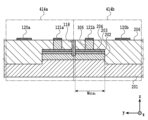
- Figure 5 shows a cross section taken along the cross section line V-V in Figure 4.
- rib type optical waveguides 414a, 414b Near the boundary between high mesa optical waveguide region A, including the connection positions with high mesa optical waveguides 113a, 113b, and high-speed modulation region/rib type optical waveguide region B, rib type optical waveguides 414a, 414b have a wide slab width W414w.
- rib type optical waveguides 414a, 414b near the boundary between high mesa optical waveguide region B, including the connection positions with high mesa optical waveguides 115a, 115b, and high mesa optical waveguide region C, rib type optical waveguides 414a, 414b have a wide slab width W414w.
- the i-type MQW core layer 204, the p-type InP layer 203, and the n-type InP lower cladding layer 202 are located in the range from the separation groove 118 to below the high-frequency lines 120a, 120b.
- the width (y direction) of the high-resistance n-type InP upper cladding layer 205 of the rib-type optical waveguides 414a, 414b is 2 ⁇ m.
- the wide slab width W414w of the i-type MQW core layer 204, p-type InP layer 203, and n-type InP lower cladding layer 202 is 30 ⁇ m.
- the length of the wide slab width W414w in the light propagation direction (x direction) is 100 ⁇ m.
- the thickness of the i-type MQW core layer 204 is 0.5 ⁇ m.
- the fundamental mode of light has a unimodal mode field with maximum intensity at the center of the 2 ⁇ m width of the high-resistance n-type InP upper cladding layer 205.
- Figures 6, 7, and 8 show cross sections taken along the lines VI-VI, VII-VII, and VIII-VIII in Figure 4, respectively.
- the rib-type optical waveguides 414a and 414b have a slab width W414n that is narrower than the wide slab width W414w.
- the portions of the rib-type optical waveguides 414a, 414b that are not loaded with the slot electrodes 121a, 121b have a slab width W414n that is narrower than the wide slab width W414w.
- the width (y direction) of the high-resistance n-type InP upper cladding layer 205 of the rib-type optical waveguides 414a, 414b at the position of the cross-sectional line VI-VI in FIG. 4 is 2 ⁇ m.
- the narrow slab width W414n of the i-type MQW core layer 204, the p-type InP layer 203, and the n-type InP lower cladding layer 202 is 13 ⁇ m, which is narrower than the wide width 414 (30 ⁇ m) at the position of the cross-sectional line V-V in FIG. 4 (FIG. 5).
- the thickness of the i-type MQW core layer 204 is 0.5 ⁇ m.
- the fundamental mode of light has a unimodal mode field with maximum intensity at the center of the 2 ⁇ m width of the high-resistance n-type InP upper cladding layer 205.
- the portions of the rib-type optical waveguides 414a, 414b on which the slot electrodes 121a, 121b are loaded have a slab width W414n that is narrower than the wide slab width W414w.
- the portions of the rib-type optical waveguides 414a, 414b have a slab width W414n that is narrower than the wide slab width W414w.
- the width (y direction) of the n-type InP upper cladding layer 305 of the rib-type optical waveguides 414a, 414b is 2 ⁇ m.
- the narrow slab width W414n of the i-type MQW core layer 204, the p-type InP layer 203, and the n-type InP lower cladding layer 202 is 13 ⁇ m, which is narrower than the wide width 414 (30 ⁇ m) at the position of the cross-sectional line V-V in FIG. 4 (FIG. 5).
- the thickness of the i-type MQW core layer 204 is 0.5 ⁇ m.
- the fundamental mode of light has a unimodal mode field with maximum intensity at the center of the 2 ⁇ m width of the n-type InP upper cladding layer 305.
- the rib-type optical waveguides 414a and 414b have a wide slab width W414w at two locations near the boundary between the high-speed modulation region/rib-type optical waveguide region B, which includes the connection positions with the high-mesa optical waveguides 113a, 113b, 115a, and 115b, and the high-mesa optical waveguide regions A and C. The reason for this is explained below.
- the slot electrodes 121a and 121b are not arranged near the boundary side between the high mesa type optical waveguide regions A and C in the high-speed modulation region and rib type optical waveguide region B, an area where the connection electrodes 122a and 122b are not arranged can be secured.
- the i-type MQW core layer 204, p-type InP layer 203, and n-type InP lower cladding layer 202 are not arranged directly below the connection electrodes 122a and 122b.
- connection electrodes 122a and 122b Since high frequency waves also flow in the connection electrodes 122a and 122b, the deterioration of high frequency characteristics is minimized by not providing semiconductors such as the i-type MQW core layer 204, p-type InP layer 203, and n-type InP lower cladding layer 202 directly below the connection electrodes 122a and 122b.
- Figure 9 shows a high-speed optical modulator 900 according to a modified embodiment of the high-speed optical modulator 400 of Figure 4.
- the high-speed modulation region and rib-type optical waveguide region B of the high-speed optical modulator 900 shown in Figure 9 includes rib-type optical waveguides 914a and 914b connected to the high-mesa optical waveguides 113a and 113b and the high-mesa optical waveguides 115a and 115b, respectively.
- each optical waveguide has a tapered shape at the boundary between the two regions to suppress optical connection loss.
- a plurality of slot electrodes 121a and 121b are formed discretely above the rib-type optical waveguides 914a and 914b, respectively, and function as an optical modulator that adds a signal to light by the electro-optic effect.
- the multiple slot electrodes 121a, 121b are connected to the two high-frequency lines 120a, 120b by multiple connection electrodes 122a, 122b, respectively.
- the two high-frequency lines 120a, 120b are formed parallel to the rib-type optical waveguides 914a, 914b above the organic film (e.g., BCB) 206, which is a non-semiconductor material, in order to propagate the RF modulated electrical signal with low loss.
- the multiple connection electrodes 122a, 122b are formed perpendicular to the rib-type optical waveguides 414a, 414b.
- the layer structure of the InP semiconductor of the rib-type optical waveguides 414a and 414b is similar to the layer structure of the InP semiconductor of the rib-type optical waveguides 114a and 114b described with reference to FIG. 3.
- the rib-type optical waveguides 914a, 914b have a wide width not only near the boundary between the high-mesa optical waveguide region A, which includes the connection positions with the high-mesa optical waveguides 113a, 113b, and the high-speed modulation region/rib-type optical waveguide region B, but also between the multiple connection electrodes 122a, 122b arranged in the light propagation direction within the high-speed modulation region/rib-type optical waveguide region B.
- a portion of the rib-type optical waveguide in the high-speed modulation region and rib-type optical waveguide region B is made wide (e.g., 30 ⁇ m), and the remaining portion is made narrow (e.g., 13 ⁇ m).
- This is equivalent to a configuration in which slab waveguides of different widths are connected in series.
- the shape and effective refractive index of the higher-order mode when the core width in the optical waveguide is 13 ⁇ m differs from that of the higher-order mode when the core width is 30 ⁇ m, so mode mismatch occurs at the connection point of the slab waveguide, resulting in loss.
- the fundamental mode which is the main mode
- the fundamental mode is confined to the upper cladding width of about 2 ⁇ m, so it propagates without feeling the width of the slab waveguide, such as 13 ⁇ m or 30 ⁇ m, and is therefore less affected.
- the higher-order mode is removed, and deterioration of the extinction ratio is suppressed.
- the i-type MQW core layer 204, p-type InP layer 203, and n-type InP lower cladding layer 202 are formed below the high-frequency lines 120a, 120b parallel to the rib-type optical waveguides 414a, 414b, the high-frequency characteristics will deteriorate.
- the length of the rib-type optical waveguides 414a, 414b with the wide slab width W414w in the light propagation direction (x direction) is short (for example, 100 ⁇ m), and the deterioration of the high-frequency characteristics is also limited.
- the rib-type optical waveguides 414a, 414b have two different widths (W414w and W414n), but it goes without saying that the same effect can be obtained even if the rib-type optical waveguides 414a, 414b have three or more different widths.
- High-speed phase modulator 111 High mesa type optical waveguide 112 1 ⁇ 2 demultiplexer 113a, 113b High mesa type optical waveguide 114a, 114b, 414a, 414b, 914a, 914b Rib type optical waveguide 115a, 115b High mesa type optical waveguide 116 2 ⁇ 1 multiplexer 117 High mesa type optical waveguide 118 Separation groove 120a, 120b High frequency line 121a, 121b Slot electrode 122a, 122b Connection electrode 130a, 130b Thin film heater 131a, 131b Pad 132a, 132b Wiring 150a, 150b Termination resistor 201 Semi-insulating InP substrate 202 n-type InP lower cladding layer 203 p-type InP layer 204 i-type MQW core layer 205 high-resistance InP upper cladding layer 206 organic film (BCB) 305 High resistance InP upper cladding layer 400, 900 High speed optical modulator
Landscapes
- Physics & Mathematics (AREA)
- General Physics & Mathematics (AREA)
- Optics & Photonics (AREA)
- Engineering & Computer Science (AREA)
- Microelectronics & Electronic Packaging (AREA)
- Nonlinear Science (AREA)
- Optical Modulation, Optical Deflection, Nonlinear Optics, Optical Demodulation, Optical Logic Elements (AREA)
Abstract
Description
本開示は、光変調器に関し、より詳細にはリブ型光導波路を用いた光変調器に関する。 This disclosure relates to an optical modulator, and more specifically to an optical modulator using a rib-type optical waveguide.
光通信システムの大容量化に伴い、高度な光変調方式に対応した高速光変調器が求められている。特にデジタルコヒーレント技術を用いた多値光変調器は、100Gbpsを超える大容量トランシーバ実現に大きな役割を果たしている。多値光変調器は、入力された光を2つのアーム光導波路に分波し、アーム光導波路を伝搬する光を変調して位相を整合させた後に合波して干渉出力するマッハツェンダ(Mach-Zehnder interferometer:MZ)干渉型の光導波路(MZ光導波路)で構成された、ゼロチャープ駆動が可能な光変調器(以下、MZ modulator:MZMという)が並列多段に内蔵されている。このような構成により、光の振幅及び位相に、それぞれ独立の信号を付加させることができる。 As optical communication systems become more capacitive, there is a demand for high-speed optical modulators compatible with advanced optical modulation methods. In particular, multilevel optical modulators using digital coherent technology are playing a major role in realizing high-capacity transceivers that exceed 100 Gbps. A multilevel optical modulator splits the input light into two arm optical waveguides, modulates the light propagating through the arm optical waveguides, aligns the phase, and then combines and outputs the resulting interference. The multilevel optical modulator has multiple parallel-stage built-in optical modulators (hereafter referred to as MZ modulators: MZMs) capable of zero-chirp drive. This configuration allows independent signals to be added to the amplitude and phase of the light.
現在、通信網への普及が進んでいる代表的な偏波多重IQ光変調器は、親MZMの各アームのそれぞれが子MZMで構成された、いわゆる入れ子構造を有する。X、Yの偏波チャネルのそれぞれに対応して子MZMが2つ並列に設けられ、計4つの子MZMを有するMZM(Quad-parallel MZM)が構成される。各々の子MZMの2つのアームには、光導波路内を伝搬する光信号に変調動作を行うためのRF変調電気信号が入力される進行波型電極が設けられている。各偏波チャネルにおいて、このような対をなす2つの子MZMの一方がIチャネル、他方がQチャネルに対応する。 Typical polarization multiplexing IQ optical modulators, which are currently being used in communication networks, have a so-called nested structure, in which each arm of a parent MZM is composed of a child MZM. Two child MZMs are provided in parallel corresponding to each of the X and Y polarization channels, forming an MZM (Quad-parallel MZM) with a total of four child MZMs. The two arms of each child MZM are provided with traveling wave type electrodes to which an RF modulated electrical signal is input to perform a modulation operation on the optical signal propagating in the optical waveguide. In each polarization channel, one of the two such paired child MZMs corresponds to the I channel and the other to the Q channel.
かかる偏波多重IQ光変調器は、子MZMのアーム光導波路に沿って設けられた変調電極の一端にRF変調電気信号を入力することにより、電気光学効果を生じさせて子MZMの光導波路内を伝搬する2つの光信号に位相変調を施している(たとえば特許文献1参照)。 Such a polarization multiplexed IQ optical modulator applies phase modulation to two optical signals propagating within the optical waveguide of the child MZM by inputting an RF modulated electrical signal to one end of a modulation electrode provided along the arm optical waveguide of the child MZM, thereby generating an electro-optic effect (see, for example, Patent Document 1).
図1に、偏波多重IQ光変調器における基本ユニットとなる子MZMに相当するマッハツェンダ干渉計を用いた高速位相変調器の一例を示す。初めに、高速位相変調器の構成について説明する。図1に示す高速位相変調器100において、1本のハイメサ型光導波路111が、ハイメサ型の光導波路構造をもつ1×2分波器112と接続されている。1×2分波器112は、2本のハイメサ型光導波路113a、113bと接続されている。ハイメサ型光導波路113a、113bは、リブ型光導波路114a、114bとそれぞれ接続されている。リブ型光導波路114a、114bは、ハイメサ型光導波路115a、115bとそれぞれ接続されている。2本のリブ型光導波路114a、114bは、分離溝118により、分離されている。ハイメサ型光導波路115a、115bは、ハイメサ型の光導波路構造をもつ2×1合波器116と接続されている。2×1合波器116は1本のハイメサ型光導波路117と接続されている。
FIG. 1 shows an example of a high-speed phase modulator using a Mach-Zehnder interferometer, which corresponds to the child MZM that is the basic unit in a polarization multiplexing IQ optical modulator. First, the configuration of the high-speed phase modulator will be described. In the high-
ハイメサ型光導波路113a、113b、リブ型光導波路114a、114b、およびハイメサ型光導波路115a、115bは、1×2分波器112と2×1合波器116間を接続するアーム光導波路を構成する。高速位相変調器100において、光の伝搬方向(x方向)に延伸する2本の高周波線路120a、120bが、アーム光導波路に沿って形成されている。高周波線路120a、120bの端部は、終端抵抗150a、150bに接続されている。リブ型光導波路114a、114bの上方に、複数のスロット電極121a、121bがそれぞれ離散的に形成されており、電気光学効果により光に信号を付加する光変調器として機能する。複数のスロット電極121a、121bは、複数の接続電極122a、122bにより2本の高周波線路120a、120bとそれぞれ接続されている。ハイメサ型光導波路115a、115bは、上方に薄膜ヒータ130a、130bがそれぞれ装荷されており、熱光学位相器として機能する。薄膜ヒータ130a、130bは、配線132a、132bにより2つのパッド131a、131bとそれぞれ接続されている。
The high mesa type
図1に示すように、高速位相変調器100は、ハイメサ型光導波路111、1×2分波器112、およびハイメサ型光導波路113a、113bを含む、ハイメサ型光導波路領域Aと、リブ型光導波路114a、114bを含む高速変調領域兼リブ型光導波路領域Bと、ハイメサ型光導波路151、115b、2×1合波器116、およびハイメサ型光導波路117を含むハイメサ型光導波路領域Cとに区分することができる。2つの領域の境界において、各光導波路は、テーパ形状を有し、光の接続損失を抑制している。
As shown in FIG. 1, the high-
図2に、図1の断面線II-IIにおける断面を示す。図2を参照して、ハイメサ型光導波路113a、113bを説明する。ハイメサ型光導波路113a、113bは、半絶縁性InP基板201上に、n型InP下部クラッド層202、p型InP層203、i型MQW(Multi Quantum Well:多重量子井戸)コア層204、および高抵抗(もしくはノンドープ)InP上部クラッド層205を積層した構造を有している。尚、高抵抗InP上部クラッド層205は、n型InP上部クラッド層をエッチングし再成長により置き換えたものである。高抵抗InP上部クラッド層205に置き換えることによって、光の伝搬損失を低減することができる。高抵抗InP上部クラッド層205とi型MQWコア層204の光の伝搬方向に直交する横方向(y方向)の幅W113は均一で数μ幅(例えば、2μm幅)である。ハイメサ型光導波路113a、113bの横方向(y方向)は有機膜(BCB:ベンゾシクロブテン)206で覆われており、i型MQWコア層204と有機膜206と間の大きな屈折率差によって横方向の光閉じ込めを実現している。
Figure 2 shows a cross section taken along line II-II in Figure 1. The high mesa
図3に、図1の断面線III-IIIにおける断面を示す。図3を参照して、リブ型光導波路114a、114bを説明する。リブ型光導波路114a、114bのInP半導体の層構造は、図2を参照して説明したハイメサ型光導波路113a、113bと類似であるが、上部クラッド層が異なる。図2のハイメサ型光導波路113a、113bの上部クラッド層は高抵抗(もしくはノンドープ)InP上部クラッド層205であるのに対して、図3のリブ型光導波路114a、114bの上部クラッド層は、n型InP上部クラッド層305となっている点で異なる。図3のリブ型光導波路114a、114bは、上部クラッド層をn型InP上部クラッド層305とすることにより電気的なコンタクトが得られ、i型MQWコア層204へ電界を印可することが可能となる。
Figure 3 shows a cross section taken along line III-III in Figure 1. The rib type
また、n型InP上部クラッド層305の横方向(y方向)の幅(y方向)は、i型MQWコア層204およびp型InP層203、およびn型InP下部クラッド層202のスラブ幅W114に比べて狭く構成されている。高速変調領域兼リブ型光導波路領域Bにおいて、スラブ幅W114は均一である。これにより、リブ型光導波路114a、114bは、n型InP上部クラッド層305の幅に相当した横方向の閉じ込め効果によって光を閉じ込める。このリブ型光導波路114a、114bには、高速位相変調を行うために離散的にリブ型光導波路の上に金属のスロット電極121a、121bが装荷され電気的なコンタクトをとっている。これにより、リブ型光導波路領域Bが高速位相変調を行う高速位相変調領域を兼ねるようにしている。高速位相変調領域Bにおけるアーム光導波路をリブ型光導波路とすることで、光が集中する領域にi型MQWコア層104のエッチングにより形成された側壁がないことから暗電流を抑制することができ、長期安定性の優れた高速位相変調器を実現することができる。
The width (y direction) of the n-type InP
上述した高速位相変調器100は、高速変調領域Bにおいてリブ型光導波路114a、114bの高抵抗InP上部クラッド層305の幅を、i型MQWコア層204、p型InP層203、およびn型InP下部クラッド層202のスラブ幅W114より狭くすることで、高抵抗InP上部クラッド層305の幅に相当した横方向の閉じ込め効果によって光を閉じ込める。また、i型MQWコア層204およびp型InP層203、およびn型InP下部クラッド層202のスラブ幅W114は、十分に広くすることによって、不要なモードが水平方向に広がり除去される効果が得られる。したがって、スラブ幅W114を広くすることが望ましい。
The above-mentioned high-
しかしながら、高速なRF変調電気信号を伝搬させる高周波線路120a、120bをリブ型光導波路114a、114bの近傍に配置する必要があり、i型MQWコア層204、p型InP層203、およびn型InP下部クラッド層202のスラブ幅W114を十分に広くすることができない。高周波線路120a、120bの下部にi型MQWコア層204、p型InP層203、およびn型InP下部クラッド層202が存在すると、インピーダンスが大きくずれ、高周波線路120a、120bにおける高周波特性の劣化(たとえば高周波の伝搬損失の増大等)が生じてしまう。以上の理由により、従来は、スラブ幅W114は13μm程度に設計される。
However, the high-
リブ型光導波路114a、114bにおけるスラブ幅W114が13μmの時、ハイメサ型光導波路113a、113bとリブ型光導波路114a、114bとの接続箇所において伝搬する光のモード中心ずれ等によって高次モードへの結合が発生した場合、高次モードが励振される。励振された高次モードは、単峰性のモードフィールドではなく、複数の光強度ピークを持つモードフィールドであり、放射することなく、リブ型光導波路114a、114bのi型MQWコア層204内に留まり伝搬することになる。さらに高次モードは、リブ型光導波路114a、114bとハイメサ型光導波路115a、115bとの接続箇所において再結合してしまい、マッハツェンダ干渉計として消光しなくなる(消光比の劣化)といった問題が発生する。
When the slab width W114 in the rib-type
本開示は、このような問題に鑑みてなされたもので、その目的とするところは、光学特性の優れた高速光変調器を提供することにある。 This disclosure was made in consideration of these problems, and its purpose is to provide a high-speed optical modulator with excellent optical characteristics.
このような目的を達成するために、本開示の一実施形態にかかる光変調器は、第1のハイメサ型光導波路と、第1のハイメサ型光導波路と接続されたハイメサ型の光導波路構造を有する分波器と、第2のハイメサ型光導波路と、第2のハイメサ型光導波路と接続されたハイメサ型の光導波路構造を有する合波器と、分波器および合波器と接続された2つのアーム光導波路と、を備え、2つのアーム光導波路の各々は、リブ型光導波路と、リブ型光導波路の上に配置された電極と、を備え、リブ型光導波路は、基板の上に順に、下部クラッド層、コア層、および上部クラッド層を含み、光の伝搬方向と直交した断面において、上部クラッド層の幅がコア層および下部クラッド層の幅より狭く、コア層および下部クラッド層の幅は、第1の幅と第1の幅よりも広い第2の幅を含む2種類以上の異なる幅を含む。 In order to achieve such an object, an optical modulator according to an embodiment of the present disclosure includes a first high-mesa optical waveguide, a splitter having a high-mesa optical waveguide structure connected to the first high-mesa optical waveguide, a second high-mesa optical waveguide, a multiplexer having a high-mesa optical waveguide structure connected to the second high-mesa optical waveguide, and two arm optical waveguides connected to the splitter and the multiplexer, each of the two arm optical waveguides including a rib-type optical waveguide and an electrode disposed on the rib-type optical waveguide, the rib-type optical waveguide including a lower cladding layer, a core layer, and an upper cladding layer in that order on a substrate, and in a cross section perpendicular to the light propagation direction, the width of the upper cladding layer is narrower than the widths of the core layer and the lower cladding layer, and the widths of the core layer and the lower cladding layer include two or more different widths including a first width and a second width wider than the first width.
以上説明したように、本開示の一実施形態によれば、光学特性の優れた高速光変調器を提供することができる。 As described above, one embodiment of the present disclosure can provide a high-speed optical modulator with excellent optical characteristics.
以下に、図面を参照しながら本開示の実施形態にかかる光変調器を詳細に説明する。同一または類似の符号は、同一または類似の要素を示し、繰り返しの説明を省略する場合がある。以下の説明における数値および材料は例示であり、本開示の要旨を逸脱しない限り他の数値および材料で本開示にかかる光変調器を実施することができる。 Below, the optical modulator according to the embodiment of the present disclosure will be described in detail with reference to the drawings. The same or similar symbols indicate the same or similar elements, and repeated explanations may be omitted. The numerical values and materials in the following description are examples, and the optical modulator according to the present disclosure can be implemented with other numerical values and materials without departing from the gist of the present disclosure.
(実施形態)
図4に、本開示の実施形態にかかる高速光変調器を示す。図4に示す高速光変調器400は、偏波多重IQ光変調器における基本ユニットとなる子MZMに相当するマッハツェンダ干渉計を用いた高速位相変調器である。高速光変調器400は、図1の高速位相変調器100と類似する点が多い。以下、高速光変調器400の高速位相変調器100と異なる点を中心に説明する。
(Embodiment)
Fig. 4 shows a high-speed optical modulator according to an embodiment of the present disclosure. The high-speed
高速光変調器400は、図1の高速位相変調器100と同様に、ハイメサ型光導波路領域Aと、高速変調領域兼リブ型光導波路領域Bと、ハイメサ型光導波路領域Cとに区分することができる。高速光変調器400におけるハイメサ型光導波路領域Aは、高速位相変調器100と同様に、ハイメサ型光導波路111、1×2分波器112、およびハイメサ型光導波路113a、113bを含む。高速光変調器400におけるハイメサ型光導波路領域Cは、高速位相変調器100と同様に、ハイメサ型光導波路115a、115b、2×1合波器116、およびハイメサ型光導波路117を含む。
The high-speed
高速光変調器400の高速変調領域兼リブ型光導波路領域Bは、ハイメサ型光導波路113a、113bおよびハイメサ型光導波路115a、115bとそれぞれ接続されたリブ型光導波路414a、414bを含む。2つの領域の境界において、各光導波路は、テーパ形状を有し、光の接続損失を抑制している。リブ型光導波路414a、414bの上方に、複数のスロット電極121a、121bがそれぞれ離散的に形成されており、電気光学効果により光に信号を付加する光変調器として機能する。複数のスロット電極121a、121bは、複数の接続電極122a、122bにより2本の高周波線路120a、120bとそれぞれ接続されている。2本の高周波線路120a、120bは、低損失でRF変調電気信号を伝搬させるために、非半導体材料である有機膜(たとえばBCB)206の上方にリブ型光導波路414a、414bと平行に形成されている。複数の接続電極122a、122bは、リブ型光導波路414a、414bに対して直角に形成されている。
The high-speed modulation region and rib-type optical waveguide region B of the high-speed
リブ型光導波路414a、414bのInP半導体の層構造は、図3を参照して説明したリブ型光導波路114a、114bのInP半導体の層構造と同様である。
The layer structure of the InP semiconductor of the rib-type
図3を参照して上述したように、高速位相変調器100の高速変調領域兼リブ型光導波路領域Bにおける、リブ型光導波路114a、114bの光の伝搬方向に直交する横方向(y方向)のスラブ幅W114は均一である。これに対して、本実施形態に係る高速光変調器400は、リブ型光導波路414a、414bの幅が、均一ではなく、不連続に変化する点で、高速位相変調器100と異なる。図5、および図6から図8を参照して後述するように、リブ型光導波路414a、414bの幅は、不連続に相対的に広いスラブ幅W414wと狭いスラブ幅W414nとの間で変化する。ここで「不連続に」とは、リブ型光導波路414a、414bの幅が、光の導波方向に沿って広いスラブ幅W414wと狭いスラブ幅W414nとの間で徐々にまたは滑らかに変化するものではないことを意図している。すなわち、「不連続に」とは、広いスラブ幅W414wから狭いスラブ幅W414nに急に変化することを意図している。
As described above with reference to FIG. 3, the slab width W114 in the lateral direction (y direction) perpendicular to the light propagation direction of the rib-type
図5に、図4の断面線V-Vにおける断面を示す。ハイメサ型光導波路113a、113bとの接続位置を含むハイメサ型光導波路領域Aと高速変調領域兼リブ型光導波路領域Bとの境界側の付近において、リブ型光導波路414a、414bは、広いスラブ幅W414wを有している。図4から理解されるように、ハイメサ型光導波路115a、115bと接続位置を含む高速変調領域兼リブ型光導波路領域Bとハイメサ型光導波路領域Cとの境界側の付近において、リブ型光導波路414a、414bは、広いスラブ幅W414wを有している。広いスラブ幅W414wを有するリブ型光導波路414a、414bの部分においては、i型MQWコア層204、p型InP層203、およびn型InP下部クラッド層202は、分離溝118から高周波線路120a、120bの下までの範囲に位置している。
Figure 5 shows a cross section taken along the cross section line V-V in Figure 4. Near the boundary between high mesa optical waveguide region A, including the connection positions with high mesa
図4の断面線V-Vの位置において、リブ型光導波路414a、414bの高抵抗n型InP上部クラッド層205の幅(y方向)は2μmである。i型MQWコア層204、p型InP層203、およびn型InP下部クラッド層202の広いスラブ幅W414wは30μmである。広いスラブ幅W414wの光の伝搬方向(x方向)の長さは100μmである。i型MQWコア層204の厚さは0.5μmである。光の基本モードは高抵抗n型InP上部クラッド層205の2μm幅の中心に最大強度を有する単峰性のモードフィールドをもっている。
At the position of the cross-sectional line V-V in FIG. 4, the width (y direction) of the high-resistance n-type InP
図6、7、8に、図4の断面線VI-VI、VII-VII、VIII-VIIIにおける断面をそれぞれ示す。ハイメサ型光導波路領域A側およびハイメサ型光導波路領域C側の広いスラブ幅W414wを有するリブ型光導波路414a、414bの部分の間において、リブ型光導波路414a、414bは、広いスラブ幅W414wよりも狭いスラブ幅W414nを有している。
Figures 6, 7, and 8 show cross sections taken along the lines VI-VI, VII-VII, and VIII-VIII in Figure 4, respectively. Between the portions of the rib-type
図6に示すように、スロット電極121a、121bが装荷されていないリブ型光導波路414a、414bの部分は、広いスラブ幅W414wよりも狭いスラブ幅W414nを有している。
As shown in FIG. 6, the portions of the rib-type
図4の断面線VI-VIの位置においてリブ型光導波路414a、414bの高抵抗n型InP上部クラッド層205の幅(y方向)は2μmである。i型MQWコア層204、p型InP層203、およびn型InP下部クラッド層202の狭いスラブ幅W414nは13μmであり、図4の断面線V-Vの位置(図5)の広い幅414(30μm)より狭い。i型MQWコア層204の厚さは0.5μmである。光の基本モードは高抵抗n型InP上部クラッド層205の2μm幅の中心に最大強度を有する単峰性のモードフィールドをもっている。
The width (y direction) of the high-resistance n-type InP
図7に示すように、スロット電極121a、121bが装荷されているリブ型光導波路414a、414bの部分は、広いスラブ幅W414wよりも狭いスラブ幅W414nを有している。
As shown in FIG. 7, the portions of the rib-type
また、図8に示すように、スロット電極121a、121bと高周波線路120a、120bとを接続する接続電極122a、122bが配置された位置において、リブ型光導波路414a、414bの部分は、広いスラブ幅W414wよりも狭いスラブ幅W414nを有している。
Also, as shown in FIG. 8, at the positions where the
図4の断面線VII-VII、およびVIII-VIIIの位置において、リブ型光導波路414a、414bのn型InP上部クラッド層305の幅(y方向)は2μmである。i型MQWコア層204、p型InP層203、およびn型InP下部クラッド層202の狭いスラブ幅W414nは13μmであり、図4の断面線V-Vの位置(図5)の広い幅414(30μm)より狭い。i型MQWコア層204の厚さは0.5μmである。光の基本モードはn型InP上部クラッド層305の2μm幅の中心に最大強度を有する単峰性のモードフィールドをもっている。
At the positions of the cross-sectional lines VII-VII and VIII-VIII in FIG. 4, the width (y direction) of the n-type InP
上述したように、本実施形態では、ハイメサ型光導波路113a、113b、115a、115bとの接続位置を含む高速変調領域兼リブ型光導波路領域Bとハイメサ型光導波路領域AおよびCとの境界側の付近の2箇所において、リブ型光導波路414a、414bは、広いスラブ幅W414wを有している。この理由を以下に説明する。
As described above, in this embodiment, the rib-type
ハイメサ型光導波路113a、113b、115a、115bとリブ型光導波路414a、414bとの2箇所の接続位置において、モードフィールドの中心ずれ等によって高次モードが励振するが、接続位置近傍のリブ型光導波路414a、414bにおける幅414nを広くしておくことによって、励振された高次モードがコア層に留まって導波しなくなる。したがって、本実施形態のように2箇所の接続位置を含む高速変調領域兼リブ型光導波路領域Bとハイメサ型光導波路領域AおよびCとの境界側の付近において、リブ型光導波路414a、414bの幅を広くすることが有効であるためである。
At the two connection positions between the high mesa
また、高速変調領域兼リブ型光導波路領域B内のハイメサ型光導波路領域AおよびCとの境界側の付近に、スロット電極121a、121bを配置しないため、接続電極122a、122bを配置していない領域を確保できる。つまり、接続電極122a、122bの直下にはi型MQWコア層204、p型InP層203、n型InP下部クラッド層202を設けないことにしている。接続電極122a、122bにも高周波は流れるため、接続電極122a、122bの直下にi型MQWコア層204、p型InP層203、n型InP下部クラッド層202のような半導体を設けないことで高周波特性の劣化を最小限としている。
In addition, since the
(変形形態)
上記のことから理解されるように、接続電極122a、122bが設置される位置を避けて、光の伝搬方向に配列された複数の接続電極122a、122bの間において、リブ型光導波路414a、414bの幅を広げることで、高次モードの除去率を高めるとともに、高周波特性の劣化を限定的とする構成も有効である。
(Modifications)
As can be understood from the above, by widening the width of the rib-type
図9に、図4の高速光変調器400の変形形態に係る高速光変調器900を示す。図9に示す高速光変調器900の高速変調領域兼リブ型光導波路領域Bは、ハイメサ型光導波路113a、113bおよびハイメサ型光導波路115a、115bとそれぞれ接続されたリブ型光導波路914a、914bを含む。図4の高速光変調器400と同様に、2つの領域の境界において、各光導波路は、テーパ形状を有し、光の接続損失を抑制している。リブ型光導波路914a、914bの上方に、複数のスロット電極121a、121bがそれぞれ離散的に形成されており、電気光学効果により光に信号を付加する光変調器として機能する。複数のスロット電極121a、121bは、複数の接続電極122a、122bにより2本の高周波線路120a、120bとそれぞれ接続されている。2本の高周波線路120a、120bは、低損失でRF変調電気信号を伝搬させるために、非半導体材料である有機膜(たとえばBCB)206の上方にリブ型光導波路914a、914bと平行に形成されている。複数の接続電極122a、122bは、リブ型光導波路414a、414bに対して直角に形成されている。
Figure 9 shows a high-speed
リブ型光導波路414a、414bのInP半導体の層構造は、図3を参照して説明したリブ型光導波路114a、114bのInP半導体の層構造と同様である。
The layer structure of the InP semiconductor of the rib-type
図9に示す高速光変調器900において、リブ型光導波路914a、914bは、ハイメサ型光導波路113a、113bと接続位置を含むハイメサ型光導波路領域Aと高速変調領域兼リブ型光導波路領域Bとの境界側の付近に加えて、高速変調領域兼リブ型光導波路領域B内の光の伝搬方向に配列された複数の接続電極122a、122bの間にも、広い幅を有している。
In the high-speed
以上において説明したように本開示の高速光変調器では、高速変調領域兼リブ型光導波路領域Bにおけるリブ型光導波路の一部を広い幅(たとえば30μm)とし、残りの部分を狭い幅(たとえば13μm)としている。幅が異なるスラブ導波路が縦列に接続されたのと同等の構成となる。光導波路におけるコアの幅が13μmのときの高次モードとコアの幅が30μmのときの高次モードでは、高次モードの形状や実効屈折率が異なるため、スラブ導波路の接続箇所にてモード不整合が発生し損失となる。一方、主モードとなる基本モードは、約2μmの上部クラッド幅程度に閉じ込められるため、13μmや30μmといったスラブ導波路の幅を感じることなく伝搬するため、影響は少ない。この結果、高次モードのみが除去され、消光比劣化が抑制される。 As described above, in the high-speed optical modulator of the present disclosure, a portion of the rib-type optical waveguide in the high-speed modulation region and rib-type optical waveguide region B is made wide (e.g., 30 μm), and the remaining portion is made narrow (e.g., 13 μm). This is equivalent to a configuration in which slab waveguides of different widths are connected in series. The shape and effective refractive index of the higher-order mode when the core width in the optical waveguide is 13 μm differs from that of the higher-order mode when the core width is 30 μm, so mode mismatch occurs at the connection point of the slab waveguide, resulting in loss. On the other hand, the fundamental mode, which is the main mode, is confined to the upper cladding width of about 2 μm, so it propagates without feeling the width of the slab waveguide, such as 13 μm or 30 μm, and is therefore less affected. As a result, only the higher-order mode is removed, and deterioration of the extinction ratio is suppressed.
尚、図5に示すように、リブ型光導波路414a、414bと平行な高周波線路120a、120bの下方にi型MQWコア層204、p型InP層203、およびn型InP下部クラッド層202が形成されると高周波特性劣化する。しかしながら、本実施形態にかかる光変調器400では、広いスラブ幅W414wを有するリブ型光導波路414a、414bの光の伝搬方向(x方向)の長さは短く(たとえば100μm)であり、高周波特性の劣化も限定的である。
As shown in Figure 5, if the i-type
なお、本開示の実施態様では、リブ型光導波路414a、414bが2種類の幅(W414wとW414n)を有する例を示したが、リブ型光導波路414a、414bが3種類以上幅を有していても同等の効果があることはいうまでもない。
In the embodiment of the present disclosure, an example is shown in which the rib-type
本開示の一実施形態によれば、光学特性の優れた高速光変調器を提供することができる。 According to one embodiment of the present disclosure, it is possible to provide a high-speed optical modulator with excellent optical characteristics.
100 高速位相変調器
111 ハイメサ型光導波路
112 1×2分波器
113a、113b ハイメサ型光導波路
114a、114b、414a、414b、914a、914b リブ型光導波路
115a、115b ハイメサ型光導波路
116 2×1合波器
117 ハイメサ型光導波路
118 分離溝
120a、120b 高周波線路
121a、121b スロット電極
122a、122b 接続電極
130a、130b 薄膜ヒータ
131a、131b パッド
132a、132b 配線
150a、150b 終端抵抗
201 半絶縁性InP基板
202 n型InP下部クラッド層
203 p型InP層
204 i型MQWコア層
205 高抵抗InP上部クラッド層
206 有機膜(BCB)
305 高抵抗InP上部クラッド層
400、900 高速光変調器
100 High-
305 High resistance InP
Claims (3)
前記第1のハイメサ型光導波路と接続されたハイメサ型の光導波路構造を有する分波器と、
第2のハイメサ型光導波路と、
前記第2のハイメサ型光導波路と接続されたハイメサ型の光導波路構造を有する合波器と、
前記分波器および前記合波器と接続された2つのアーム光導波路と、
を備えた光変調器であって、
前記2つのアーム光導波路の各々は、
リブ型光導波路と、
前記リブ型光導波路の上に配置された電極と、
を備え、
前記リブ型光導波路は、
基板の上に順に、下部クラッド層、コア層、および上部クラッド層を含み、
光の伝搬方向と直交した断面において、前記上部クラッド層の幅が前記コア層および前記下部クラッド層の幅より狭く、
前記コア層および前記下部クラッド層の幅は、第1の幅と前記第1の幅よりも広い第2の幅を含む2種類以上の異なる幅を含む、光変調器。 A first high mesa type optical waveguide;
a demultiplexer having a high mesa type optical waveguide structure connected to the first high mesa type optical waveguide;
A second high mesa type optical waveguide;
a multiplexer having a high mesa type optical waveguide structure connected to the second high mesa type optical waveguide;
two arm optical waveguides connected to the demultiplexer and the multiplexer;
An optical modulator comprising:
Each of the two arm optical waveguides has
A rib-type optical waveguide;
an electrode disposed on the rib-type optical waveguide;
Equipped with
The rib type optical waveguide is
a lower clad layer, a core layer, and an upper clad layer, in that order, on a substrate;
In a cross section perpendicular to the direction of light propagation, the width of the upper clad layer is narrower than the widths of the core layer and the lower clad layer,
An optical modulator, wherein the widths of the core layer and the lower cladding layer include two or more different widths including a first width and a second width wider than the first width.
前記光の伝搬方向と直交した断面において、前記第2の幅を有する前記コア層および前記下部クラッド層は、前記高周波線路と前記基板の間に配置されている、請求項1に記載の光変調器。 a high-frequency line arranged in parallel to the rib-type optical waveguide,
2. The optical modulator according to claim 1, wherein in a cross section perpendicular to the propagation direction of the light, the core layer having the second width and the lower cladding layer are disposed between the high-frequency line and the substrate.
前記分波器および前記リブ型光導波路と接続された第3のハイメサ型光導波路と、
リブ型光導波路および前記合波器と接続された第4のハイメサ型光導波路と、
をさらに備え、
前記第2の幅を有する前記コア層および前記下部クラッド層は、前記リブ型光導波路と前記第3のハイメサ型光導波路との接続位置の近傍、および前記リブ型光導波路と前記第4のハイメサ型光導波路との接続位置の近傍に配置されている、請求項1または2に記載の光変調器。 Each of the two arm optical waveguides has
a third high mesa type optical waveguide connected to the demultiplexer and the rib type optical waveguide;
a fourth high mesa type optical waveguide connected to the rib type optical waveguide and the multiplexer; and
Further equipped with
3. The optical modulator according to claim 1, wherein the core layer and the lower cladding layer having the second width are arranged near a connection position between the rib type optical waveguide and the third high mesa type optical waveguide and near a connection position between the rib type optical waveguide and the fourth high mesa type optical waveguide.
Priority Applications (2)
| Application Number | Priority Date | Filing Date | Title |
|---|---|---|---|
| JP2025525504A JPWO2024252534A1 (en) | 2023-06-06 | 2023-06-06 | |
| PCT/JP2023/021061 WO2024252534A1 (en) | 2023-06-06 | 2023-06-06 | Optical modulator |
Applications Claiming Priority (1)
| Application Number | Priority Date | Filing Date | Title |
|---|---|---|---|
| PCT/JP2023/021061 WO2024252534A1 (en) | 2023-06-06 | 2023-06-06 | Optical modulator |
Publications (1)
| Publication Number | Publication Date |
|---|---|
| WO2024252534A1 true WO2024252534A1 (en) | 2024-12-12 |
Family
ID=93795481
Family Applications (1)
| Application Number | Title | Priority Date | Filing Date |
|---|---|---|---|
| PCT/JP2023/021061 Ceased WO2024252534A1 (en) | 2023-06-06 | 2023-06-06 | Optical modulator |
Country Status (2)
| Country | Link |
|---|---|
| JP (1) | JPWO2024252534A1 (en) |
| WO (1) | WO2024252534A1 (en) |
Citations (5)
| Publication number | Priority date | Publication date | Assignee | Title |
|---|---|---|---|---|
| JPH063708A (en) * | 1992-06-19 | 1994-01-14 | Nippon Telegr & Teleph Corp <Ntt> | Optical switch and manufacturing method thereof |
| US20030039447A1 (en) * | 2001-08-27 | 2003-02-27 | Clapp Terry V. | Strip-loaded optical waveguide |
| WO2010100946A1 (en) * | 2009-03-05 | 2010-09-10 | 日本電気株式会社 | Semiconductor optical modulator, semiconductor optical integrated device, and method for manufacturing the same |
| WO2019156189A1 (en) * | 2018-02-08 | 2019-08-15 | 古河電気工業株式会社 | Optical integrated element and optical module |
| WO2019211991A1 (en) * | 2018-05-01 | 2019-11-07 | 日本電信電話株式会社 | Semiconductor mach-zehnder optical modulator and iq optical modulator using same |
-
2023
- 2023-06-06 JP JP2025525504A patent/JPWO2024252534A1/ja active Pending
- 2023-06-06 WO PCT/JP2023/021061 patent/WO2024252534A1/en not_active Ceased
Patent Citations (5)
| Publication number | Priority date | Publication date | Assignee | Title |
|---|---|---|---|---|
| JPH063708A (en) * | 1992-06-19 | 1994-01-14 | Nippon Telegr & Teleph Corp <Ntt> | Optical switch and manufacturing method thereof |
| US20030039447A1 (en) * | 2001-08-27 | 2003-02-27 | Clapp Terry V. | Strip-loaded optical waveguide |
| WO2010100946A1 (en) * | 2009-03-05 | 2010-09-10 | 日本電気株式会社 | Semiconductor optical modulator, semiconductor optical integrated device, and method for manufacturing the same |
| WO2019156189A1 (en) * | 2018-02-08 | 2019-08-15 | 古河電気工業株式会社 | Optical integrated element and optical module |
| WO2019211991A1 (en) * | 2018-05-01 | 2019-11-07 | 日本電信電話株式会社 | Semiconductor mach-zehnder optical modulator and iq optical modulator using same |
Also Published As
| Publication number | Publication date |
|---|---|
| JPWO2024252534A1 (en) | 2024-12-12 |
Similar Documents
| Publication | Publication Date | Title |
|---|---|---|
| US8412008B2 (en) | Semiconductor optical device | |
| US8412005B2 (en) | Mach-Zehnder interferometer type optical modulator | |
| US11275287B2 (en) | Semiconductor Mach-Zehnder optical modulator and IQ optical modulator using same | |
| US10027088B2 (en) | Integrated semiconductor optical element and manufacturing method for same | |
| EP4369082A1 (en) | Electro-optic modulator and electro-optic device | |
| US20030091287A1 (en) | Multimode interference (MMI) device | |
| JP6126541B2 (en) | Semiconductor Mach-Zehnder optical modulator | |
| EP3913425B1 (en) | Semiconductor mach zehnder optical modulator | |
| JP7356050B2 (en) | optical switch device | |
| JP5917645B2 (en) | Optical switch element | |
| JP6348880B2 (en) | Semiconductor Mach-Zehnder optical modulator | |
| CA3153651C (en) | Semiconductor mach-zehnder optical modulator and iq modulator | |
| WO2024252534A1 (en) | Optical modulator | |
| JP2019045666A (en) | Semiconductor Mach-Zehnder Optical Modulator and IQ Modulator | |
| JP2014191218A (en) | Optical modulator | |
| WO2019235392A1 (en) | Optical switch device | |
| US20220091472A1 (en) | Optical Switch Element | |
| JP2007094336A (en) | Optical semiconductor device and method for manufacturing optical semiconductor device | |
| JP2016114712A (en) | Semiconductor Mach-Zehnder optical modulator | |
| WO2019176665A1 (en) | Optical modulator | |
| JP2011133582A (en) | Semiconductor mach-zehnder type optical modulator and method of manufacturing the same | |
| JP6023028B2 (en) | Optical switch element | |
| JP2014191085A (en) | Optical modulator | |
| JP4209357B2 (en) | Semiconductor optical modulator | |
| WO2024247046A1 (en) | Optical modulator |
Legal Events
| Date | Code | Title | Description |
|---|---|---|---|
| 121 | Ep: the epo has been informed by wipo that ep was designated in this application |
Ref document number: 23940639 Country of ref document: EP Kind code of ref document: A1 |
|
| ENP | Entry into the national phase |
Ref document number: 2025525504 Country of ref document: JP Kind code of ref document: A |
|
| NENP | Non-entry into the national phase |
Ref country code: DE |