WO2024252654A1 - Diode - Google Patents
Diode Download PDFInfo
- Publication number
- WO2024252654A1 WO2024252654A1 PCT/JP2023/021462 JP2023021462W WO2024252654A1 WO 2024252654 A1 WO2024252654 A1 WO 2024252654A1 JP 2023021462 W JP2023021462 W JP 2023021462W WO 2024252654 A1 WO2024252654 A1 WO 2024252654A1
- Authority
- WO
- WIPO (PCT)
- Prior art keywords
- semiconductor layer
- region
- diode
- layer
- anode electrode
- Prior art date
- Legal status (The legal status is an assumption and is not a legal conclusion. Google has not performed a legal analysis and makes no representation as to the accuracy of the status listed.)
- Ceased
Links
Images


Classifications
-
- H—ELECTRICITY
- H10—SEMICONDUCTOR DEVICES; ELECTRIC SOLID-STATE DEVICES NOT OTHERWISE PROVIDED FOR
- H10D—INORGANIC ELECTRIC SEMICONDUCTOR DEVICES
- H10D8/00—Diodes
- H10D8/50—PIN diodes
-
- H—ELECTRICITY
- H10—SEMICONDUCTOR DEVICES; ELECTRIC SOLID-STATE DEVICES NOT OTHERWISE PROVIDED FOR
- H10D—INORGANIC ELECTRIC SEMICONDUCTOR DEVICES
- H10D8/00—Diodes
- H10D8/60—Schottky-barrier diodes
Definitions
- the present invention relates to a diode made of AlN.
- AlN has a high figure of merit, and the drift layer can be made thinner than that of GaN or Si. This allows the on-resistance to be reduced even further than that of devices using GaN, making it a promising material system for ultra-high voltage power devices and switching devices.
- power devices include Schottky barrier diodes (SBDs) and p-n junction diodes (PNDs).
- the SBD is composed of an anode electrode, a cathode electrode, an n-type semiconductor layer (drift layer), and an n + semiconductor layer.
- the anode electrode is provided with an electrode material made of metal so as to form a Schottky junction with the n-type semiconductor layer.
- the semiconductor layer is composed of GaN
- a Ni-based material is used as the anode electrode that forms a Schottky junction.
- the cathode electrode and the n + semiconductor layer are made of materials that form an ohmic contact.
- metal materials such as Ti/Al/Ni/Au are used. These may be annealed to reduce the contact resistance with the semiconductor layer.
- SBDs are unipolar devices in which electrons that overcome the Schottky barrier between the anode electrode and the n-type semiconductor layer contribute to conduction as majority carriers, and are generally capable of high-speed operation. In addition, the rise in I-V characteristics is good. However, when increasing the withstand voltage, the drift layer must be made thicker and the impurity concentration must be reduced, which has the disadvantage of increasing the on-resistance. For this reason, SBDs are often used in low-withstand voltage applications.
- PNDs are composed of a p-type semiconductor layer, an n-type semiconductor layer, and a low-concentration n-type semiconductor layer (i-type semiconductor layer), and both the p-side anode electrode and the n-side cathode electrode form ohmic contacts with the p-type semiconductor layer and the n-type semiconductor layer.
- PNDs are bipolar devices, and both electrons and holes are involved in conduction. In the conductive state, carriers accumulate in the i-semiconductor layer from both the p-side and the n-side, making it possible to achieve large currents with a relatively low on-resistance. For this reason, PNDs are often used in large current and high voltage applications.
- JBS Junction barrier Schottky diodes
- JBS has two types of regions: a first region in which a p-type layer and an electrode that makes ohmic contact with the p-type layer are stacked on an n-type layer, and a second region in which the p-type layer is removed and an electrode that forms a Schottky contact with the n-type layer is formed.
- the second region operates as an SBD, and has high speed operation and good start-up behavior.
- the first region operates as a PND, and during high current operation, a large amount of carriers are accumulated at the pn junction, reducing the on-resistance.
- the device characteristics can be adjusted by the area ratio of the first region to the second region.
- the JBS structure can achieve high-speed operation, steep rise operation, and low on-resistance at large currents.
- AlN has an even higher ionization energy of impurities during p-type doping than GaN, making it a difficult material to make p-type.
- Mg a typical dopant for p-type doping, is said to have an ionization energy of 500-600 meV.
- some light-emitting elements such as LEDs
- the present invention was made to solve the above problems, and aims to provide a junction barrier Schottky diode using AlN.
- the diode according to the present invention comprises an n-type first semiconductor layer made of AlN having group III polarity, a second semiconductor layer made of AlGaN having group III polarity and formed on a first region of the first semiconductor layer, a third semiconductor layer made of a p-type nitride semiconductor having group III polarity and formed on the second semiconductor layer, a first anode electrode formed on the third semiconductor layer in ohmic contact, a second anode electrode formed on a second region other than the first region of the first semiconductor layer in Schottky contact and at the same potential as the first anode electrode, and a cathode electrode electrically connected to the first semiconductor layer, the second semiconductor layer having a smaller Al composition on the third semiconductor layer side than on the first semiconductor layer side in the thickness direction, and the third semiconductor layer being made of GaN or AlGaN with an Al composition difference between the second semiconductor layer and the third semiconductor layer in contact with the third semiconductor layer being less than 0.1.
- a second semiconductor layer made of AlGaN and a third semiconductor layer made of a p-type nitride semiconductor are formed on an n-type first semiconductor layer made of AlN, which is called a drift layer, and the second semiconductor layer has a smaller Al composition on the third semiconductor layer side than on the first semiconductor layer side in the thickness direction, so that a junction barrier Schottky diode using AlN can be provided.
- FIG. 1 is a cross-sectional view showing the structure of a diode according to an embodiment of the present invention.
- FIG. 2 is a cross-sectional view showing the structure of another diode according to an embodiment of the present invention.
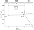
- FIG. 3A is a band diagram showing a band structure at 300K of a diode according to an embodiment.
- FIG. 3B is a band diagram showing an expanded band structure of the valence band portion at 300 K of the diode according to the embodiment.
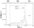
- FIG. 4 is a characteristic diagram showing the plot results of the hole concentration distribution near the interface between the second semiconductor layer 102 and the first semiconductor layer 101 when the initial composition x of the second semiconductor layer 102 is changed from 0.5 to 1.0.
- FIG. 1 is a cross-sectional view showing the structure of a diode according to an embodiment of the present invention.
- FIG. 2 is a cross-sectional view showing the structure of another diode according to an embodiment of the present invention.
- FIG. 3A is a band diagram
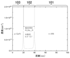
- FIG. 5A is a band diagram showing the band structure at 300 K of a diode according to an embodiment in which the composition of the second semiconductor layer 102 at the starting point on the first semiconductor layer 101 side is 0.7 and the composition of the ending point on the third semiconductor layer 103 side is 0.3.
- FIG. 5B is a characteristic diagram showing the plot of the hole concentration distribution near the interface between the second semiconductor layer 102 and the first semiconductor layer 101 when the Al composition at the starting point of the second semiconductor layer 102 on the first semiconductor layer 101 side is 0.7 and the Al composition at the ending point on the third semiconductor layer 103 side is 0.3.
- FIG. 5A is a band diagram showing the band structure at 300 K of a diode according to an embodiment in which the composition of the second semiconductor layer 102 at the starting point on the first semiconductor layer 101 side is 0.7 and the composition of the ending point on the third semiconductor layer 103 side is 0.3.
- FIG. 5B is a characteristic diagram showing the plot of the hole concentration distribution near the interface between the second semiconductor layer 102 and the first
- FIG. 6A is a cross-sectional view showing a state of a diode in the middle of a process for explaining a method of manufacturing a diode according to an embodiment of the present invention.
- FIG. 6B is a cross-sectional view showing a state of the diode in the middle of a process for explaining a method for manufacturing a diode according to an embodiment of the present invention.
- FIG. 6C is a cross-sectional view showing a state of a diode in the middle of a process for explaining a method of manufacturing a diode according to an embodiment of the present invention.
- FIG. 6D is a cross-sectional view showing a state of a diode in the middle of a process for explaining a method for manufacturing a diode according to an embodiment of the present invention.
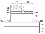
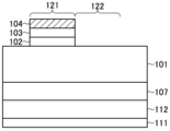
- This diode comprises a first semiconductor layer 101, a second semiconductor layer 102, a third semiconductor layer 103, a first anode electrode 104, a second anode electrode 105, and a cathode electrode 106.
- This diode is a junction barrier Schottky diode (JBS) comprising a first region 121 that constitutes a p-n junction diode (PND) and a second region 122 that constitutes a Schottky barrier diode (SBD).
- JBS junction barrier Schottky diode
- PND p-n junction diode
- SBD Schottky barrier diode
- the first region 121 and the second region 122 are disposed adjacent to each other.
- the first semiconductor layer 101 is made of AlN having group III polarity and is n-type.
- the first semiconductor layer 101 is called a drift layer.
- the first semiconductor layer 101 can be made n-type by doping it with Si as an impurity to about 1 ⁇ 10 17 cm ⁇ 3 .
- the first semiconductor layer 101 can have a thickness of 200 nm.
- the dopant is not limited to Si, and any dopant may be used as long as it is capable of n-type doping within a practical range.
- the doping concentration of the drift layer is set low to ensure a high breakdown voltage.
- the dielectric breakdown field is large and the figure of merit is high, so that even if the impurity concentration of the first semiconductor layer 101 is set to about 10 17 cm ⁇ 3 , the device can be designed without sacrificing the on-resistance.
- the doping concentration of the first semiconductor layer 101 can be reduced and made thicker.
- the first semiconductor layer 101 can be made higher in concentration and thinner, or lower in concentration and thicker, depending on the application.
- the second semiconductor layer 102 is made of AlGaN that is group III polarity.
- the second semiconductor layer 102 is formed on and in contact with the first region 121 of the first semiconductor layer 101.
- the second semiconductor layer 102 may have a thickness of, for example, 20 nm.
- the second semiconductor layer 102 is not intentionally doped.
- the second semiconductor layer 102 has a smaller Al composition on the third semiconductor layer 103 side than on the first semiconductor layer 101 side in the thickness direction.
- the second semiconductor layer 102 has a smaller Al composition as it moves away from the first semiconductor layer 101 in the thickness direction.
- the second semiconductor layer 102 starts from Al 0.7 Ga 0.3 N with an Al composition of 0.7 on the first semiconductor layer 101 side, and the composition smoothly changes to a state where the Al composition is almost 0, and is connected (contacted) to the third semiconductor layer 103.
- the second semiconductor layer 102 can also be composed of multiple layers with different compositions on the first semiconductor layer 101 side and the third semiconductor layer 103 side. Even in this case, the layer on the third semiconductor layer 103 side has a smaller Al composition than the layer on the first semiconductor layer 101 side.
- the third semiconductor layer 103 is made of a p-type nitride semiconductor with group III polarity and is formed on and in contact with the second semiconductor layer 102.
- the third semiconductor layer 103 is made of GaN or AlGaN with an Al composition difference between the third semiconductor layer 103 and the second semiconductor layer 102 in contact with the third semiconductor layer 103 being less than 0.1.
- the third semiconductor layer 103 can have a thickness of 20 nm and a doping concentration of 5 ⁇ 10 18 cm ⁇ 3 , for example.
- the third semiconductor layer 103 can be made of GaN, but since the critical thickness of the GaN layer on the AlN layer is about several nm, if the thickness is set to 20 nm, the stress and strain are quickly relaxed during the crystal growth. In this relaxation, a large amount of crystal defects are also introduced, but since the third semiconductor layer 103 is a layer doped with a high concentration of p-type impurities and is not a drift layer that affects the breakdown voltage, the influence of the crystal defects introduced by lattice relaxation is small. Furthermore, if the third semiconductor layer 103 is appropriately designed, it can also be made of AlGaN that forms p-type conduction and has a smaller Al composition than AlN. These will be described later.
- the first anode electrode 104 is formed in ohmic contact on the third semiconductor layer 103.
- the second anode electrode 105 is formed in Schottky contact on the second region 122 other than the first region 121 of the first semiconductor layer 101.
- the second anode electrode 105 is at the same potential as the first anode electrode 104.
- the cathode electrode 106 is electrically connected to the first semiconductor layer 101.
- the first semiconductor layer 101 can be formed on the upper surface of a contact layer 107 made of AlN that has been doped with Si to be of n + type and have low resistance, and the cathode electrode 106 can be formed on the lower surface of the contact layer 107 in ohmic contact.
- a buffer layer 112 and a contact layer 107 can be formed in sequence on a substrate 111, and a first semiconductor layer 101, a second semiconductor layer 102, a third semiconductor layer 103, a first anode electrode 104, a second anode electrode 105, and a cathode electrode 106 can be formed in an element region on the contact layer 107.
- the cathode electrode 106 can be formed on the contact layer 107 on the side of the element region. Also, as shown in FIG.
- the second anode electrode 105 can be formed extending into the first region 121, and the portion of the second anode electrode 105 extending into the first region 121 can be formed in contact with the first anode electrode 104. With this configuration, the second anode electrode 105 and the first anode electrode 104 can be at the same potential.
- the substrate 111 is selected from a suitable substrate for crystal growth of AlN, which is the main material constituting the first semiconductor layer 101.
- suitable substrate for crystal growth of AlN examples include SiC (silicon carbide), Al 2 O 3 (sapphire), and single crystal AlN substrates.
- the buffer layer 112 made of AlN, the contact layer 107, the first semiconductor layer 101, the second semiconductor layer 102, and the third semiconductor layer 103 are formed in sequence, and each layer has a c-plane as the main surface and has a group III polarity.
- a nitride semiconductor usually grows with group III polarity.
- the buffer layer 112 is formed to a thickness required to improve the crystal quality during crystal growth.
- the buffer layer 112 can be omitted by forming the contact layer 107, which makes ohmic contact with the cathode electrode 106, thick.
- the contact layer 107 must be in ohmic contact with the cathode electrode 106, so its resistance is made as low as possible.
- the contact layer 107 can be made to have a superlattice structure such as AlGaN/AlN to reduce its resistance. Note that forming a thick superlattice structure makes it easier for crystal defects such as cracks to be introduced, so the thickness of the contact layer 107 is designed with this in mind.
- the buffer layer 112 is formed on the substrate 111, the contact layer 107 is formed on the buffer layer 112, and the first semiconductor layer 101 is formed on top of this.
- the substrate 111 is made of low-resistance SiC or Si, and the buffer layer 112 also has a low resistance.
- the series resistance in the contact layer 107 may affect the operation of the diode.
- the series resistance in the contact layer 107 described above can be reduced by providing the cathode electrode 106 on the lower surface side of the contact layer 107 and configuring the current to flow through the substrate 111 in the thickness direction (stacking direction).
- FIG. 3A shows the band structure at 300K. It is assumed that the first semiconductor layer 101 and the second semiconductor layer 102 are pseudo-lattice matched to AlN, and the third semiconductor layer 103 is lattice-relaxed with respect to AlN.
- the second semiconductor layer 102 made of Al x Ga 1-x N is set so that the Al composition x decreases continuously from the first semiconductor layer 101 side to the third semiconductor layer 103.
- the starting composition on the first semiconductor layer 101 side is plotted by changing it in increments of 0.1 in the range from 1.0 to 0.5.
- FIG. 3B is an enlarged view focusing on the valence band portion of FIG. 3A.
- Nitride semiconductors such as AlN and GaN are materials that have polarization in the c-axis direction, and when a heterostructure is formed, a polarization electric field is generated at the interface due to spontaneous polarization and piezoelectric polarization caused by strain. Therefore, the smaller the starting Al composition on the first semiconductor layer 101 side, the larger the polarization electric field at the interface between the first semiconductor layer 101 and the second semiconductor layer 102, and the more the band is bent.
- Figure 4 shows the results of plotting the hole concentration distribution when the starting composition x of the second semiconductor layer 102 is changed from 0.5 to 1.0. It can be seen that as the starting composition x decreases from 0.9, the peak hole concentration near the interface between the second semiconductor layer 102 and the first semiconductor layer 101 increases dramatically.
- the conduction band is also bent by the polarization electric field.
- a two-dimensional electron gas (2DEG) is formed instead of a 2DHG.
- 2DEG two-dimensional electron gas
- the third semiconductor layer 103 is introduced to avoid the generation of 2DEG.
- the concentration of 2DHG increases as the starting composition of the second semiconductor layer 102 decreases to 0.5, in other words, as the difference in composition with the first semiconductor layer 101 increases. Therefore, if a GaN layer could be formed directly on the first semiconductor layer 101, it is expected that a higher 2DHG would be obtained.
- the critical thickness of GaN on AlN is extremely small, at a few nm. For this reason, it is difficult to form a GaN layer of the same thickness as the second semiconductor layer 102, which is 20 nm thick, on the first semiconductor layer 101 without relaxing the stress and strain. If the stress and strain are relaxed, it is difficult to form the 2DHG as described above due to increased interface roughness and increased crystal defect density.
- the second semiconductor layer 102 in order to form the second semiconductor layer 102 while maintaining a practical thickness of 10 nm or more, it is desirable to configure the second semiconductor layer 102 from Al x Ga 1-x N and set the initial composition x to at least 0.3.
- the initial composition x is 1.0, 2DHG does not occur effectively. For these reasons, it is effective to set the initial composition x to less than 1.0 and 0.3 or more.
- Figure 5A is a band diagram when the composition of the starting point of the second semiconductor layer 102 on the first semiconductor layer 101 side is 0.7, and the composition of the ending point on the third semiconductor layer 103 side is 0.3. Also, Figure 5B shows the change in hole concentration when the Al composition of the starting point of the second semiconductor layer 102 on the first semiconductor layer 101 side is 0.7, and the Al composition of the ending point on the third semiconductor layer 103 side is 0.3.
- the composition difference is small, the formation of the second 2DHG can be suppressed.
- the Al composition at the end point is about 0.1, the formation of the 2DHG can be almost suppressed. Therefore, by making the Al composition difference between the end point of the second semiconductor layer 102 and the third semiconductor layer 103 smaller than 0.1, the formation of the 2DHG in the vicinity of the interface between them can be almost suppressed. This makes it possible to bring out more of the effect of the 2DHG formed in the vicinity of the interface between the first semiconductor layer 101 and the second semiconductor layer 102.
- the third semiconductor layer 103 is made of GaN, it is desirable to set the Al composition x at the interface between the second semiconductor layer 102 made of Al x Ga 1-x N and the third semiconductor layer 103 to 0.1 or less.
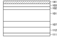
- non-doped AlN, n + -type AlN, n-type AlN, AlGaN with a gradually decreasing Al composition in the growth direction, and p-type GaN are epitaxially grown by metalorganic vapor phase epitaxy to form a buffer layer 112, a contact layer 107, a first semiconductor layer 101, a second semiconductor layer 102, and a third semiconductor layer 103, as shown in FIG. 6A.
- a metal that is in ohmic contact with p-type GaN is deposited on the third semiconductor layer 103 to form a metal layer 141.
- a heat treatment is performed to form an ohmic contact between the third semiconductor layer 103 and the metal layer 141.
- the second semiconductor layer 102, the third semiconductor layer 103, and the metal layer 141 are patterned by known lithography techniques and dry etching techniques such as ICP-RIE, thereby forming the columnar second semiconductor layer 102, the third semiconductor layer 103, and the first anode electrode 104 in the first region 121, as shown in FIG. 6B. It is not easy to stop the above-mentioned etching process at the interface between the first semiconductor layer 101 and the second semiconductor layer 102, but there is no problem even if the first semiconductor layer 101 in regions other than the first region 121, including the second region 122, is etched to some extent.
- the first semiconductor layer 101 is patterned by known lithography techniques and dry etching techniques such as ICP-RIE, to process the first region 121 and the second region 122 into a columnar shape in order to separate the elements, as shown in FIG. 6C.
- the first semiconductor layer 101 is etched in this patterning process until the contact layer 107 is exposed.
- a cathode electrode 106 is formed on the contact layer 107 exposed around the columnar first semiconductor layer 101.
- the first region 121 and the second region 122 are each formed in one location, but this is not limited to the above.
- the second region 122 can be formed in each of multiple locations of the first semiconductor layer 101
- the first region 121 can be formed in each of multiple locations of the first semiconductor layer 101 (see Non-Patent Document 1).
- a second semiconductor layer made of AlGaN and a third semiconductor layer made of a p-type nitride semiconductor are formed on an n-type first semiconductor layer made of AlN, which is called a drift layer, and the second semiconductor layer has a smaller Al composition on the third semiconductor layer side than on the first semiconductor layer side in the thickness direction, so that a junction barrier Schottky diode using AlN can be provided.
- 101 first semiconductor layer
- 102 second semiconductor layer
- 103 third semiconductor layer
- 104 first anode electrode
- 105 second anode electrode
- 106 cathode electrode
- 107 contact layer
- 121 first region
- 122 second region.
Landscapes
- Electrodes Of Semiconductors (AREA)
Abstract
L'invention concerne une diode qui comprend : une première couche de semiconducteur (101) ; une deuxième couche de semiconducteur (102) ; une troisième couche de semiconducteur (103) ; une première électrode d'anode (104) ; une seconde électrode d'anode (105) ; et une électrode de cathode (106). Cette diode comprend en outre : une première région (121) qui constitue une diode à jonction p-n ; et une seconde région (122) qui constitue une diode à barrière de Schottky (SBD). La seconde couche de semiconducteur (102) est composée d'AlGaN, qui a une polarité du groupe III. La seconde couche semi-conductrice (102) est formée au-dessus et en contact avec la première région (121) de la première couche semi-conductrice (101). En outre, la deuxième couche semi-conductrice (102) a une composition d'Al plus petite sur le côté de la troisième couche semi-conductrice (103) que sur le côté de la première couche semi-conductrice (101) dans la direction de l'épaisseur.
Priority Applications (2)
| Application Number | Priority Date | Filing Date | Title |
|---|---|---|---|
| PCT/JP2023/021462 WO2024252654A1 (fr) | 2023-06-09 | 2023-06-09 | Diode |
| JP2025525899A JPWO2024252654A1 (fr) | 2023-06-09 | 2023-06-09 |
Applications Claiming Priority (1)
| Application Number | Priority Date | Filing Date | Title |
|---|---|---|---|
| PCT/JP2023/021462 WO2024252654A1 (fr) | 2023-06-09 | 2023-06-09 | Diode |
Publications (1)
| Publication Number | Publication Date |
|---|---|
| WO2024252654A1 true WO2024252654A1 (fr) | 2024-12-12 |
Family
ID=93795520
Family Applications (1)
| Application Number | Title | Priority Date | Filing Date |
|---|---|---|---|
| PCT/JP2023/021462 Ceased WO2024252654A1 (fr) | 2023-06-09 | 2023-06-09 | Diode |
Country Status (2)
| Country | Link |
|---|---|
| JP (1) | JPWO2024252654A1 (fr) |
| WO (1) | WO2024252654A1 (fr) |
Citations (3)
| Publication number | Priority date | Publication date | Assignee | Title |
|---|---|---|---|---|
| JP2011071356A (ja) * | 2009-09-26 | 2011-04-07 | Sanken Electric Co Ltd | 半導体装置 |
| JP2018133444A (ja) * | 2017-02-15 | 2018-08-23 | トヨタ自動車株式会社 | 窒化物半導体装置 |
| WO2020218294A1 (fr) * | 2019-04-25 | 2020-10-29 | 京セラ株式会社 | Dispositif à semi-conducteur et procédé de fabrication de dispositif à semi-conducteur |
-
2023
- 2023-06-09 JP JP2025525899A patent/JPWO2024252654A1/ja active Pending
- 2023-06-09 WO PCT/JP2023/021462 patent/WO2024252654A1/fr not_active Ceased
Patent Citations (3)
| Publication number | Priority date | Publication date | Assignee | Title |
|---|---|---|---|---|
| JP2011071356A (ja) * | 2009-09-26 | 2011-04-07 | Sanken Electric Co Ltd | 半導体装置 |
| JP2018133444A (ja) * | 2017-02-15 | 2018-08-23 | トヨタ自動車株式会社 | 窒化物半導体装置 |
| WO2020218294A1 (fr) * | 2019-04-25 | 2020-10-29 | 京セラ株式会社 | Dispositif à semi-conducteur et procédé de fabrication de dispositif à semi-conducteur |
Non-Patent Citations (4)
| Title |
|---|
| AHMAD HABIB; ENGEL ZACHARY; MATTHEWS CHRISTOPHER M.; LEE SANGHO; DOOLITTLE W. ALAN: "Realization of homojunction PN AlN diodes", JOURNAL OF APPLIED PHYSICS, AMERICAN INSTITUTE OF PHYSICS, 2 HUNTINGTON QUADRANGLE, MELVILLE, NY 11747, vol. 131, no. 17, 2 May 2022 (2022-05-02), 2 Huntington Quadrangle, Melville, NY 11747, XP012265408, ISSN: 0021-8979, DOI: 10.1063/5.0086314 * |
| HAYASHIDA TETSURO, NANJO TAKUMA, FURUKAWA AKIHIKO, WATAHIKI TATSURO, YAMAMUKA MIKIO: "Leakage current reduction of vertical GaN junction barrier Schottky diodes using dual-anode process", JAPANESE JOURNAL OF APPLIED PHYSICS, JAPAN SOCIETY OF APPLIED PHYSICS, JP, vol. 57, no. 4, 1 April 2018 (2018-04-01), JP , pages 040302, XP093247033, ISSN: 0021-4922, DOI: 10.7567/JJAP.57.040302 * |
| HIROKI MASANOBU; TANIYASU YOSHITAKA; KUMAKURA KAZUHIDE: "High-Temperature Performance of AlN MESFETs With Epitaxially Grown n-Type AlN Channel Layers", IEEE ELECTRON DEVICE LETTERS, IEEE, USA, vol. 43, no. 3, 7 January 2022 (2022-01-07), USA, pages 350 - 353, XP011901246, ISSN: 0741-3106, DOI: 10.1109/LED.2022.3141100 * |
| NI XIANFENG; FAN QIAN; HUA BIN; SUN PEIHAO; CAI ZHENGZHI; WANG HSIN-CHUAN; HUANG C. N.; GU XING: "Improvement of AlN Material Quality by High-Temperature Annealing Toward Power Diodes", IEEE TRANSACTIONS ON ELECTRON DEVICES, IEEE, USA, vol. 67, no. 10, 29 May 2020 (2020-05-29), USA, pages 3988 - 3991, XP011811082, ISSN: 0018-9383, DOI: 10.1109/TED.2020.2991397 * |
Also Published As
| Publication number | Publication date |
|---|---|
| JPWO2024252654A1 (fr) | 2024-12-12 |
Similar Documents
| Publication | Publication Date | Title |
|---|---|---|
| US10707324B2 (en) | Group IIIA-N HEMT with a tunnel diode in the gate stack | |
| US11222985B2 (en) | Power semiconductor device | |
| JP6371986B2 (ja) | 窒化物半導体構造物 | |
| JP5564842B2 (ja) | 半導体装置 | |
| CN113725296B (zh) | 氮化物半导体外延叠层结构及其功率元件 | |
| KR102011761B1 (ko) | 이중 금속의 부분 리세스된 전극을 갖는 GaN계 쇼트키 다이오드 | |
| JP6308478B2 (ja) | 一部が凹んだアノードを有するGaN系ショットキーダイオード | |
| US20030151042A1 (en) | Polarization field enhanced tunnel structures | |
| JP5190923B2 (ja) | GaNをチャネル層とする窒化物半導体トランジスタ及びその作製方法 | |
| JP5997234B2 (ja) | 半導体装置、電界効果トランジスタおよび電子装置 | |
| US9564491B2 (en) | Semiconductor device | |
| TWI641133B (zh) | 半導體單元 | |
| US9450112B2 (en) | GaN-based Schottky barrier diode with algan surface layer | |
| JP6225584B2 (ja) | 半導体装置の評価方法、並びに半導体装置およびその製造方法 | |
| TWI569439B (zh) | 半導體單元 | |
| JP4986472B2 (ja) | 窒化物半導体構造 | |
| US8044485B2 (en) | Semiconductor device | |
| TW201911421A (zh) | 三族氮化物高速電子遷移率場效應電晶體元件 | |
| JP5701805B2 (ja) | 窒化物半導体ショットキダイオードの製造方法 | |
| WO2024252654A1 (fr) | Diode | |
| JP2010177416A (ja) | 窒化物半導体装置 | |
| JP2019054015A (ja) | 窒化物半導体装置 | |
| US20160013327A1 (en) | Nitride semiconductor diode | |
| KR20140117840A (ko) | 혼합 접합 드레인을 구비하는 질화물 반도체 소자 및 그 제조 방법 | |
| JP5956616B2 (ja) | 窒化物半導体ショットキダイオード |
Legal Events
| Date | Code | Title | Description |
|---|---|---|---|
| 121 | Ep: the epo has been informed by wipo that ep was designated in this application |
Ref document number: 23940752 Country of ref document: EP Kind code of ref document: A1 |
|
| ENP | Entry into the national phase |
Ref document number: 2025525899 Country of ref document: JP Kind code of ref document: A |
|
| WWE | Wipo information: entry into national phase |
Ref document number: 2025525899 Country of ref document: JP |
|
| NENP | Non-entry into the national phase |
Ref country code: DE |