WO2024252654A1 - ダイオード - Google Patents
ダイオード Download PDFInfo
- Publication number
- WO2024252654A1 WO2024252654A1 PCT/JP2023/021462 JP2023021462W WO2024252654A1 WO 2024252654 A1 WO2024252654 A1 WO 2024252654A1 JP 2023021462 W JP2023021462 W JP 2023021462W WO 2024252654 A1 WO2024252654 A1 WO 2024252654A1
- Authority
- WO
- WIPO (PCT)
- Prior art keywords
- semiconductor layer
- region
- diode
- layer
- anode electrode
- Prior art date
- Legal status (The legal status is an assumption and is not a legal conclusion. Google has not performed a legal analysis and makes no representation as to the accuracy of the status listed.)
- Ceased
Links
Images


Classifications
-
- H—ELECTRICITY
- H10—SEMICONDUCTOR DEVICES; ELECTRIC SOLID-STATE DEVICES NOT OTHERWISE PROVIDED FOR
- H10D—INORGANIC ELECTRIC SEMICONDUCTOR DEVICES
- H10D8/00—Diodes
- H10D8/50—PIN diodes
-
- H—ELECTRICITY
- H10—SEMICONDUCTOR DEVICES; ELECTRIC SOLID-STATE DEVICES NOT OTHERWISE PROVIDED FOR
- H10D—INORGANIC ELECTRIC SEMICONDUCTOR DEVICES
- H10D8/00—Diodes
- H10D8/60—Schottky-barrier diodes
Definitions
- the present invention relates to a diode made of AlN.
- AlN has a high figure of merit, and the drift layer can be made thinner than that of GaN or Si. This allows the on-resistance to be reduced even further than that of devices using GaN, making it a promising material system for ultra-high voltage power devices and switching devices.
- power devices include Schottky barrier diodes (SBDs) and p-n junction diodes (PNDs).
- the SBD is composed of an anode electrode, a cathode electrode, an n-type semiconductor layer (drift layer), and an n + semiconductor layer.
- the anode electrode is provided with an electrode material made of metal so as to form a Schottky junction with the n-type semiconductor layer.
- the semiconductor layer is composed of GaN
- a Ni-based material is used as the anode electrode that forms a Schottky junction.
- the cathode electrode and the n + semiconductor layer are made of materials that form an ohmic contact.
- metal materials such as Ti/Al/Ni/Au are used. These may be annealed to reduce the contact resistance with the semiconductor layer.
- SBDs are unipolar devices in which electrons that overcome the Schottky barrier between the anode electrode and the n-type semiconductor layer contribute to conduction as majority carriers, and are generally capable of high-speed operation. In addition, the rise in I-V characteristics is good. However, when increasing the withstand voltage, the drift layer must be made thicker and the impurity concentration must be reduced, which has the disadvantage of increasing the on-resistance. For this reason, SBDs are often used in low-withstand voltage applications.
- PNDs are composed of a p-type semiconductor layer, an n-type semiconductor layer, and a low-concentration n-type semiconductor layer (i-type semiconductor layer), and both the p-side anode electrode and the n-side cathode electrode form ohmic contacts with the p-type semiconductor layer and the n-type semiconductor layer.
- PNDs are bipolar devices, and both electrons and holes are involved in conduction. In the conductive state, carriers accumulate in the i-semiconductor layer from both the p-side and the n-side, making it possible to achieve large currents with a relatively low on-resistance. For this reason, PNDs are often used in large current and high voltage applications.
- JBS Junction barrier Schottky diodes
- JBS has two types of regions: a first region in which a p-type layer and an electrode that makes ohmic contact with the p-type layer are stacked on an n-type layer, and a second region in which the p-type layer is removed and an electrode that forms a Schottky contact with the n-type layer is formed.
- the second region operates as an SBD, and has high speed operation and good start-up behavior.
- the first region operates as a PND, and during high current operation, a large amount of carriers are accumulated at the pn junction, reducing the on-resistance.
- the device characteristics can be adjusted by the area ratio of the first region to the second region.
- the JBS structure can achieve high-speed operation, steep rise operation, and low on-resistance at large currents.
- AlN has an even higher ionization energy of impurities during p-type doping than GaN, making it a difficult material to make p-type.
- Mg a typical dopant for p-type doping, is said to have an ionization energy of 500-600 meV.
- some light-emitting elements such as LEDs
- the present invention was made to solve the above problems, and aims to provide a junction barrier Schottky diode using AlN.
- the diode according to the present invention comprises an n-type first semiconductor layer made of AlN having group III polarity, a second semiconductor layer made of AlGaN having group III polarity and formed on a first region of the first semiconductor layer, a third semiconductor layer made of a p-type nitride semiconductor having group III polarity and formed on the second semiconductor layer, a first anode electrode formed on the third semiconductor layer in ohmic contact, a second anode electrode formed on a second region other than the first region of the first semiconductor layer in Schottky contact and at the same potential as the first anode electrode, and a cathode electrode electrically connected to the first semiconductor layer, the second semiconductor layer having a smaller Al composition on the third semiconductor layer side than on the first semiconductor layer side in the thickness direction, and the third semiconductor layer being made of GaN or AlGaN with an Al composition difference between the second semiconductor layer and the third semiconductor layer in contact with the third semiconductor layer being less than 0.1.
- a second semiconductor layer made of AlGaN and a third semiconductor layer made of a p-type nitride semiconductor are formed on an n-type first semiconductor layer made of AlN, which is called a drift layer, and the second semiconductor layer has a smaller Al composition on the third semiconductor layer side than on the first semiconductor layer side in the thickness direction, so that a junction barrier Schottky diode using AlN can be provided.
- FIG. 1 is a cross-sectional view showing the structure of a diode according to an embodiment of the present invention.
- FIG. 2 is a cross-sectional view showing the structure of another diode according to an embodiment of the present invention.
- FIG. 3A is a band diagram showing a band structure at 300K of a diode according to an embodiment.
- FIG. 3B is a band diagram showing an expanded band structure of the valence band portion at 300 K of the diode according to the embodiment.
- FIG. 4 is a characteristic diagram showing the plot results of the hole concentration distribution near the interface between the second semiconductor layer 102 and the first semiconductor layer 101 when the initial composition x of the second semiconductor layer 102 is changed from 0.5 to 1.0.
- FIG. 1 is a cross-sectional view showing the structure of a diode according to an embodiment of the present invention.
- FIG. 2 is a cross-sectional view showing the structure of another diode according to an embodiment of the present invention.
- FIG. 3A is a band diagram
- FIG. 5A is a band diagram showing the band structure at 300 K of a diode according to an embodiment in which the composition of the second semiconductor layer 102 at the starting point on the first semiconductor layer 101 side is 0.7 and the composition of the ending point on the third semiconductor layer 103 side is 0.3.
- FIG. 5B is a characteristic diagram showing the plot of the hole concentration distribution near the interface between the second semiconductor layer 102 and the first semiconductor layer 101 when the Al composition at the starting point of the second semiconductor layer 102 on the first semiconductor layer 101 side is 0.7 and the Al composition at the ending point on the third semiconductor layer 103 side is 0.3.
- FIG. 5A is a band diagram showing the band structure at 300 K of a diode according to an embodiment in which the composition of the second semiconductor layer 102 at the starting point on the first semiconductor layer 101 side is 0.7 and the composition of the ending point on the third semiconductor layer 103 side is 0.3.
- FIG. 5B is a characteristic diagram showing the plot of the hole concentration distribution near the interface between the second semiconductor layer 102 and the first
- FIG. 6A is a cross-sectional view showing a state of a diode in the middle of a process for explaining a method of manufacturing a diode according to an embodiment of the present invention.
- FIG. 6B is a cross-sectional view showing a state of the diode in the middle of a process for explaining a method for manufacturing a diode according to an embodiment of the present invention.
- FIG. 6C is a cross-sectional view showing a state of a diode in the middle of a process for explaining a method of manufacturing a diode according to an embodiment of the present invention.
- FIG. 6D is a cross-sectional view showing a state of a diode in the middle of a process for explaining a method for manufacturing a diode according to an embodiment of the present invention.
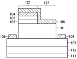
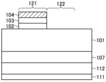
- This diode comprises a first semiconductor layer 101, a second semiconductor layer 102, a third semiconductor layer 103, a first anode electrode 104, a second anode electrode 105, and a cathode electrode 106.
- This diode is a junction barrier Schottky diode (JBS) comprising a first region 121 that constitutes a p-n junction diode (PND) and a second region 122 that constitutes a Schottky barrier diode (SBD).
- JBS junction barrier Schottky diode
- PND p-n junction diode
- SBD Schottky barrier diode
- the first region 121 and the second region 122 are disposed adjacent to each other.
- the first semiconductor layer 101 is made of AlN having group III polarity and is n-type.
- the first semiconductor layer 101 is called a drift layer.
- the first semiconductor layer 101 can be made n-type by doping it with Si as an impurity to about 1 ⁇ 10 17 cm ⁇ 3 .
- the first semiconductor layer 101 can have a thickness of 200 nm.
- the dopant is not limited to Si, and any dopant may be used as long as it is capable of n-type doping within a practical range.
- the doping concentration of the drift layer is set low to ensure a high breakdown voltage.
- the dielectric breakdown field is large and the figure of merit is high, so that even if the impurity concentration of the first semiconductor layer 101 is set to about 10 17 cm ⁇ 3 , the device can be designed without sacrificing the on-resistance.
- the doping concentration of the first semiconductor layer 101 can be reduced and made thicker.
- the first semiconductor layer 101 can be made higher in concentration and thinner, or lower in concentration and thicker, depending on the application.
- the second semiconductor layer 102 is made of AlGaN that is group III polarity.
- the second semiconductor layer 102 is formed on and in contact with the first region 121 of the first semiconductor layer 101.
- the second semiconductor layer 102 may have a thickness of, for example, 20 nm.
- the second semiconductor layer 102 is not intentionally doped.
- the second semiconductor layer 102 has a smaller Al composition on the third semiconductor layer 103 side than on the first semiconductor layer 101 side in the thickness direction.
- the second semiconductor layer 102 has a smaller Al composition as it moves away from the first semiconductor layer 101 in the thickness direction.
- the second semiconductor layer 102 starts from Al 0.7 Ga 0.3 N with an Al composition of 0.7 on the first semiconductor layer 101 side, and the composition smoothly changes to a state where the Al composition is almost 0, and is connected (contacted) to the third semiconductor layer 103.
- the second semiconductor layer 102 can also be composed of multiple layers with different compositions on the first semiconductor layer 101 side and the third semiconductor layer 103 side. Even in this case, the layer on the third semiconductor layer 103 side has a smaller Al composition than the layer on the first semiconductor layer 101 side.
- the third semiconductor layer 103 is made of a p-type nitride semiconductor with group III polarity and is formed on and in contact with the second semiconductor layer 102.
- the third semiconductor layer 103 is made of GaN or AlGaN with an Al composition difference between the third semiconductor layer 103 and the second semiconductor layer 102 in contact with the third semiconductor layer 103 being less than 0.1.
- the third semiconductor layer 103 can have a thickness of 20 nm and a doping concentration of 5 ⁇ 10 18 cm ⁇ 3 , for example.
- the third semiconductor layer 103 can be made of GaN, but since the critical thickness of the GaN layer on the AlN layer is about several nm, if the thickness is set to 20 nm, the stress and strain are quickly relaxed during the crystal growth. In this relaxation, a large amount of crystal defects are also introduced, but since the third semiconductor layer 103 is a layer doped with a high concentration of p-type impurities and is not a drift layer that affects the breakdown voltage, the influence of the crystal defects introduced by lattice relaxation is small. Furthermore, if the third semiconductor layer 103 is appropriately designed, it can also be made of AlGaN that forms p-type conduction and has a smaller Al composition than AlN. These will be described later.
- the first anode electrode 104 is formed in ohmic contact on the third semiconductor layer 103.
- the second anode electrode 105 is formed in Schottky contact on the second region 122 other than the first region 121 of the first semiconductor layer 101.
- the second anode electrode 105 is at the same potential as the first anode electrode 104.
- the cathode electrode 106 is electrically connected to the first semiconductor layer 101.
- the first semiconductor layer 101 can be formed on the upper surface of a contact layer 107 made of AlN that has been doped with Si to be of n + type and have low resistance, and the cathode electrode 106 can be formed on the lower surface of the contact layer 107 in ohmic contact.
- a buffer layer 112 and a contact layer 107 can be formed in sequence on a substrate 111, and a first semiconductor layer 101, a second semiconductor layer 102, a third semiconductor layer 103, a first anode electrode 104, a second anode electrode 105, and a cathode electrode 106 can be formed in an element region on the contact layer 107.
- the cathode electrode 106 can be formed on the contact layer 107 on the side of the element region. Also, as shown in FIG.
- the second anode electrode 105 can be formed extending into the first region 121, and the portion of the second anode electrode 105 extending into the first region 121 can be formed in contact with the first anode electrode 104. With this configuration, the second anode electrode 105 and the first anode electrode 104 can be at the same potential.
- the substrate 111 is selected from a suitable substrate for crystal growth of AlN, which is the main material constituting the first semiconductor layer 101.
- suitable substrate for crystal growth of AlN examples include SiC (silicon carbide), Al 2 O 3 (sapphire), and single crystal AlN substrates.
- the buffer layer 112 made of AlN, the contact layer 107, the first semiconductor layer 101, the second semiconductor layer 102, and the third semiconductor layer 103 are formed in sequence, and each layer has a c-plane as the main surface and has a group III polarity.
- a nitride semiconductor usually grows with group III polarity.
- the buffer layer 112 is formed to a thickness required to improve the crystal quality during crystal growth.
- the buffer layer 112 can be omitted by forming the contact layer 107, which makes ohmic contact with the cathode electrode 106, thick.
- the contact layer 107 must be in ohmic contact with the cathode electrode 106, so its resistance is made as low as possible.
- the contact layer 107 can be made to have a superlattice structure such as AlGaN/AlN to reduce its resistance. Note that forming a thick superlattice structure makes it easier for crystal defects such as cracks to be introduced, so the thickness of the contact layer 107 is designed with this in mind.
- the buffer layer 112 is formed on the substrate 111, the contact layer 107 is formed on the buffer layer 112, and the first semiconductor layer 101 is formed on top of this.
- the substrate 111 is made of low-resistance SiC or Si, and the buffer layer 112 also has a low resistance.
- the series resistance in the contact layer 107 may affect the operation of the diode.
- the series resistance in the contact layer 107 described above can be reduced by providing the cathode electrode 106 on the lower surface side of the contact layer 107 and configuring the current to flow through the substrate 111 in the thickness direction (stacking direction).
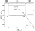
- FIG. 3A shows the band structure at 300K. It is assumed that the first semiconductor layer 101 and the second semiconductor layer 102 are pseudo-lattice matched to AlN, and the third semiconductor layer 103 is lattice-relaxed with respect to AlN.
- the second semiconductor layer 102 made of Al x Ga 1-x N is set so that the Al composition x decreases continuously from the first semiconductor layer 101 side to the third semiconductor layer 103.
- the starting composition on the first semiconductor layer 101 side is plotted by changing it in increments of 0.1 in the range from 1.0 to 0.5.
- FIG. 3B is an enlarged view focusing on the valence band portion of FIG. 3A.
- Nitride semiconductors such as AlN and GaN are materials that have polarization in the c-axis direction, and when a heterostructure is formed, a polarization electric field is generated at the interface due to spontaneous polarization and piezoelectric polarization caused by strain. Therefore, the smaller the starting Al composition on the first semiconductor layer 101 side, the larger the polarization electric field at the interface between the first semiconductor layer 101 and the second semiconductor layer 102, and the more the band is bent.
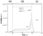
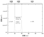
- Figure 4 shows the results of plotting the hole concentration distribution when the starting composition x of the second semiconductor layer 102 is changed from 0.5 to 1.0. It can be seen that as the starting composition x decreases from 0.9, the peak hole concentration near the interface between the second semiconductor layer 102 and the first semiconductor layer 101 increases dramatically.
- the conduction band is also bent by the polarization electric field.
- a two-dimensional electron gas (2DEG) is formed instead of a 2DHG.
- 2DEG two-dimensional electron gas
- the third semiconductor layer 103 is introduced to avoid the generation of 2DEG.
- the concentration of 2DHG increases as the starting composition of the second semiconductor layer 102 decreases to 0.5, in other words, as the difference in composition with the first semiconductor layer 101 increases. Therefore, if a GaN layer could be formed directly on the first semiconductor layer 101, it is expected that a higher 2DHG would be obtained.
- the critical thickness of GaN on AlN is extremely small, at a few nm. For this reason, it is difficult to form a GaN layer of the same thickness as the second semiconductor layer 102, which is 20 nm thick, on the first semiconductor layer 101 without relaxing the stress and strain. If the stress and strain are relaxed, it is difficult to form the 2DHG as described above due to increased interface roughness and increased crystal defect density.
- the second semiconductor layer 102 in order to form the second semiconductor layer 102 while maintaining a practical thickness of 10 nm or more, it is desirable to configure the second semiconductor layer 102 from Al x Ga 1-x N and set the initial composition x to at least 0.3.
- the initial composition x is 1.0, 2DHG does not occur effectively. For these reasons, it is effective to set the initial composition x to less than 1.0 and 0.3 or more.
- Figure 5A is a band diagram when the composition of the starting point of the second semiconductor layer 102 on the first semiconductor layer 101 side is 0.7, and the composition of the ending point on the third semiconductor layer 103 side is 0.3. Also, Figure 5B shows the change in hole concentration when the Al composition of the starting point of the second semiconductor layer 102 on the first semiconductor layer 101 side is 0.7, and the Al composition of the ending point on the third semiconductor layer 103 side is 0.3.
- the composition difference is small, the formation of the second 2DHG can be suppressed.
- the Al composition at the end point is about 0.1, the formation of the 2DHG can be almost suppressed. Therefore, by making the Al composition difference between the end point of the second semiconductor layer 102 and the third semiconductor layer 103 smaller than 0.1, the formation of the 2DHG in the vicinity of the interface between them can be almost suppressed. This makes it possible to bring out more of the effect of the 2DHG formed in the vicinity of the interface between the first semiconductor layer 101 and the second semiconductor layer 102.
- the third semiconductor layer 103 is made of GaN, it is desirable to set the Al composition x at the interface between the second semiconductor layer 102 made of Al x Ga 1-x N and the third semiconductor layer 103 to 0.1 or less.
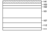
- non-doped AlN, n + -type AlN, n-type AlN, AlGaN with a gradually decreasing Al composition in the growth direction, and p-type GaN are epitaxially grown by metalorganic vapor phase epitaxy to form a buffer layer 112, a contact layer 107, a first semiconductor layer 101, a second semiconductor layer 102, and a third semiconductor layer 103, as shown in FIG. 6A.
- a metal that is in ohmic contact with p-type GaN is deposited on the third semiconductor layer 103 to form a metal layer 141.
- a heat treatment is performed to form an ohmic contact between the third semiconductor layer 103 and the metal layer 141.
- the second semiconductor layer 102, the third semiconductor layer 103, and the metal layer 141 are patterned by known lithography techniques and dry etching techniques such as ICP-RIE, thereby forming the columnar second semiconductor layer 102, the third semiconductor layer 103, and the first anode electrode 104 in the first region 121, as shown in FIG. 6B. It is not easy to stop the above-mentioned etching process at the interface between the first semiconductor layer 101 and the second semiconductor layer 102, but there is no problem even if the first semiconductor layer 101 in regions other than the first region 121, including the second region 122, is etched to some extent.
- the first semiconductor layer 101 is patterned by known lithography techniques and dry etching techniques such as ICP-RIE, to process the first region 121 and the second region 122 into a columnar shape in order to separate the elements, as shown in FIG. 6C.
- the first semiconductor layer 101 is etched in this patterning process until the contact layer 107 is exposed.
- a cathode electrode 106 is formed on the contact layer 107 exposed around the columnar first semiconductor layer 101.
- the first region 121 and the second region 122 are each formed in one location, but this is not limited to the above.
- the second region 122 can be formed in each of multiple locations of the first semiconductor layer 101
- the first region 121 can be formed in each of multiple locations of the first semiconductor layer 101 (see Non-Patent Document 1).
- a second semiconductor layer made of AlGaN and a third semiconductor layer made of a p-type nitride semiconductor are formed on an n-type first semiconductor layer made of AlN, which is called a drift layer, and the second semiconductor layer has a smaller Al composition on the third semiconductor layer side than on the first semiconductor layer side in the thickness direction, so that a junction barrier Schottky diode using AlN can be provided.
- 101 first semiconductor layer
- 102 second semiconductor layer
- 103 third semiconductor layer
- 104 first anode electrode
- 105 second anode electrode
- 106 cathode electrode
- 107 contact layer
- 121 first region
- 122 second region.
Landscapes
- Electrodes Of Semiconductors (AREA)
Abstract
このダイオードは、第1半導体層(101)、第2半導体層(102)、第3半導体層(103)、第1アノード電極(104)、第2アノード電極(105)、およびカソード電極(106)を備える。このダイオードは、p-n接合ダイオード(PND)を構成する第1領域(121)と、ショットキーバリアダイオード(SBD)を構成する第2領域(122)とを備える。第2半導体層(102)は、III族極性とされているAlGaNから構成されている。第2半導体層(102)は、第1半導体層(101)の第1領域(121)の上に接して形成されている。また、第2半導体層(102)は、厚さ方向に第1半導体層(101)の側に対して第3半導体層(103)の側のAlの組成が小さくされている。
Description
本発明は、AlNから構成したダイオードに関する。
AlNは性能指数が高く、GaNやSiに比べてドリフト層を薄くすることができる。このため、GaNを用いたデバイスよりもさらにオン抵抗を低減することができ、超高耐圧パワーデバイスや、スイッチングデバイスとして有望な材料系である。パワーデバイスとして、ショットキーバリアダイオード(SBD)およびp-n接合ダイオード(PND)がある。
SBDは、アノード電極とカソード電極、n型半導体層(ドリフト層)およびn+半導体層によって構成される。アノード電極は、n型半導体層とショットキー接合を形成するように、金属からなる電極材料を設ける。半導体層をGaNから構成する場合、ショットキー接合するアノード電極としてNi系の材料が使用される。カソード電極とn+半導体層は、オーミック接触が形成されるような材料とする。GaNの場合、Ti/Al/Ni/Auなどの金属材料が使用される。これらは、アニール処理によって半導体層とのコンタクト抵抗を低減する処理が施される場合もある。
SBDは、アノード電極とn型半導体層の間のショットキー障壁を乗り越えた電子が、多数キャリアとして伝導に寄与するユニポーラデバイスであり、一般的に高速動作が可能である。また、I-V特性の立ち上がり動作が良好である。しかし、高耐圧化する場合は、ドリフト層をより厚くして不純物濃度をより低下させることになり、オン抵抗が高くなるというデメリットもある。このため、SBDは、低耐圧用途に用いられることが多い。
一方、PNDは、p型半導体層、n型半導体層、および低濃度n型半導体層(i型半導体層)によって構成され、p側アノード電極、n側カソード電極ともに、p型半導体層、n型半導体層に対してオーミック接触を形成する。PNDはバイポーラデバイスであり、伝導に際して電子、正孔の双方が関与する。導通状態では、p側、n側の双方から、i半導体層にキャリアが蓄積され、大電流を比較的低いオン抵抗で実現可能である。このため、PNDは大電流・高耐圧用途で使用されることが多い。
ただし、PNDは、遮断状態へ移行する際に蓄積した大量のキャリアを双方の層へ吐き出さねばならず、リバースリカバリ特性がよくない。
上述したようなPNDとSBDとの一長一短の特性を補いつつ、高速動作性と、大電流・低オン抵抗化を実現可能な構造として、これらのハイブリッド構造であるジャンクションバリアショットキーダイオード(junction barrier Schottky diodes;JBS)がある(非特許文献1)。
JBSにおいては、n型層上にp型層およびp型層へオーミック接触をする電極が積層された第1領域と、p型層を除去しn型層とショットキー接触を形成する電極を形成した第2領域との2種類の領域とを備える。第2領域はSBDとして動作する領域であり、高速な動作と良好な立ち上がり動作をする。第1領域はPNDとして動作する領域であり、大電流動作時にpn接合より多量のキャリアが蓄積され、オン抵抗を低減する。デバイスの特性は第1領域と第2領域との面積比によって調整することができる。
T. Hayashida et al., "Leakage current reduction of vertical GaN junction barrier Schottky diodes using dual-anode process", Japanese Journal of Applied Physics, vol. 57, 040302, 2018.
AlNを用いたダイオードにおいても、JBS構造により高速動作・急峻な立ち上がり動作、大電流時の低オン抵抗化が実現できると考えられる。しかし、AlNは、GaNに比べてさらにp型ドーピング時の不純物のイオン化エネルギーが高く、p型化が難しい材料である。例えば典型的なp型化のドーパントであるMgですら、イオン化エネルギーは500~600meVと言われている。このため、一部の発光素子(LEDなど)を除くと、パワーデバイス用途としてのJBSはおろか実用的なPNDすら報告は少ない。
本発明は、以上のような問題点を解消するためになされたものであり、AlNを用いたジャンクションバリアショットキーダイオードの提供を目的とする。
本発明に係るダイオードは、III族極性とされているAlNから構成されたn型の第1半導体層と、III族極性とされているAlGaNから構成され、第1半導体層の第1領域の上に接して形成された第2半導体層と、III族極性とされているp型の窒化物半導体から構成されて第2半導体層の上に接して形成された第3半導体層と、第3半導体層の上にオーミック接触して形成された第1アノード電極と、第1半導体層の第1領域以外の第2領域の上にショットキー接触して形成され、第1アノード電極と同電位とされた第2アノード電極と、第1半導体層に電気的に接続するカソード電極とを備え、第2半導体層は、厚さ方向に第1半導体層の側に対して第3半導体層の側のAlの組成が小さくされ、第3半導体層は、GaNまたは第3半導体層に接する第2半導体層とのAl組成の差が0.1より小さいAlGaNから構成されている。
以上説明したように、本発明によれば、ドリフト層と呼ばれるAlNから構成したn型の第1半導体層の上に、AlGaNから構成した第2半導体層、p型の窒化物半導体から構成した第3半導体層を形成し、第2半導体層は、厚さ方向に第1半導体層の側に対して第3半導体層の側のAlの組成が小さくしたので、AlNを用いたジャンクションバリアショットキーダイオードが提供できる。
以下、本発明の実施の形態に係るダイオードについて図1を参照して説明する。このダイオードは、第1半導体層101、第2半導体層102、第3半導体層103、第1アノード電極104、第2アノード電極105、およびカソード電極106を備える。このダイオードは、p-n接合ダイオード(PND)を構成する第1領域121と、ショットキーバリアダイオード(SBD)を構成する第2領域122とを備えるジャンクションバリアショットキーダイオード(JBS)である。この例では、第1領域121と第2領域122とは、隣接して配置している。
第1半導体層101は、III族極性とされているAlNから構成されてn型とされている。第1半導体層101は、ドリフト層と呼ばれている。第1半導体層101は、例えば不純物としてSiを1×1017cm-3程度にドーピングすることでn型とすることができる。例えば、第1半導体層101は、厚さ200nmとすることができる。なお、ドーパントは、Siに限るものではなく、実用的な範囲でn型ドーピングが可能であれば如何なるドーパントであってもよい。
一般的なGaNのパワーデバイス用のp-n接合ダイオードは、耐圧を確保するためにドリフト層のドーピング濃度は低く設定される。しかし、AlNを用いる場合は、絶縁破壊電解が大きく、性能指数が高いため、第1半導体層101の不純物濃度を1017cm-3程度に設定しても、オン抵抗を犠牲にすることなくデバイス設計が可能である。さらなる高耐圧化のためには、第1半導体層101のドーピング濃度を下げ、より厚くすることができる。また、第1半導体層101は、用途に応じてさらに高濃度化・薄層化すること、また、低濃度化・厚膜化することができる。
第2半導体層102は、III族極性とされているAlGaNから構成されている。第2半導体層102は、第1半導体層101の第1領域121の上に接して形成されている。第2半導体層102は、例えば、厚さ20nmとすることができる。第2半導体層102には、意図的なドーピングは行わない。また、第2半導体層102は、厚さ方向に第1半導体層101の側に対して第3半導体層103の側のAlの組成が小さくされている。
例えば、第2半導体層102は、厚さ方向に第1半導体層101から離れるほどAlの組成が小さくされている。第2半導体層102は、例えば、第1半導体層101の側をAl組成0.7のAl0.7Ga0.3Nから初めて、Al組成がほぼ0の状態まで滑らかに組成を変化させ、第3半導体層103に接続(接触)させる。また、第2半導体層102は、第1半導体層101の側と第3半導体層103とで組成が異なる複数の層から構成することができる。この場合においても、第3半導体層103の側の層は、第1半導体層101の側の層よりAlの組成を小さくする。
第3半導体層103は、III族極性とされているp型の窒化物半導体から構成されて第2半導体層102の上に接して形成されている。第3半導体層103は、GaNまたは第3半導体層103に接する第2半導体層102とのAl組成の差が0.1より小さいAlGaNから構成されている。
第3半導体層103をp型とするドーパントとしては、典型的にはMgが用いられる。第3半導体層103は、例えば、厚さを20nm、ドーピング濃度を5×1018cm-3とすることができる。第3半導体層103は、GaNから構成することができるが、AlNの層の上へのGaNの層の臨界膜厚は数nm程度のため、厚さを20nmとすると、結晶成長の中で速やかに応力・ひずみが緩和される。この緩和においては、結晶欠陥も多量に導入されるが、第3半導体層103は、高濃度のp型不純物がドープされた層であり、耐圧に影響のあるドリフト層ではないため、格子緩和によって導入される結晶欠陥の影響は小さい。また第3半導体層103は、適切な設計を施せば、p型伝導を形成してAlNに比べてAl組成が小さいAlGaNから構成することもできる。これらについては、後述する。
第1アノード電極104は、第3半導体層103の上にオーミック接触して形成されている。第2アノード電極105は、第1半導体層101の第1領域121以外の第2領域122の上にショットキー接触して形成されている。また、第2アノード電極105は、第1アノード電極104と同電位とされている。
カソード電極106は、第1半導体層101に電気的に接続している。例えば、第1半導体層101は、Siをドーピングすることによりn+型とされて低抵抗化したAlNからなるコンタクト層107の上面に形成し、コンタクト層107の下面に、オーミック接触するカソード電極106を形成することができる。
また、図2に示すように、基板111の上に、バッファ層112、コンタクト層107を順次に形成し、コンタクト層107の上の素子領域に第1半導体層101、第2半導体層102、第3半導体層103、第1アノード電極104、第2アノード電極105、およびカソード電極106を形成することができる。このように構成し、素子領域の側方のコンタクト層107の上にカソード電極106を形成することができる。また、図2に示すように、第2アノード電極105を第1領域121に延在して形成し、第2アノード電極105の第1領域121に延在する部分を、第1アノード電極104の上に接して形成することができる。この構成とすることで、第2アノード電極105と第1アノード電極104とを同電位にすることができる。
基板111は、第1半導体層101を構成する主材料であるAlNを結晶成長するための適切な基板を選定する。例えば、SiC(シリコンカーバイド)やAl2O3(サファイア)、単結晶AlN基板が挙げられる。例えばサファイアから構成して主表面をc面とした基板111の上に、公知の有機金属気相成長法などにより窒化物半導体を結晶成長することで、AlNからなるバッファ層112、コンタクト層107、第1半導体層101、第2半導体層102、第3半導体層103を順次に形成すれば、各層は、主表面をc面としてIII族極性となる。よく知られているように、無極性の結晶であるサファイアによる主表面をC面とされた基板111の上には、通常、窒化物半導体はIII族極性で結晶成長する。
バッファ層112は、結晶成長において結晶品質を高めるうえで必要な厚さに形成する。カソード電極106をオーミック接触させるコンタクト層107を厚く形成することで、バッファ層112を省略することはできる。コンタクト層107は、カソード電極106にオーミック接触する必要があるため、できる限り低抵抗化する。例えば、コンタクト層107を、AlGaN/AlNなどの超格子構造とすることで、低抵抗化することが可能である。なお、超格子構造を厚く形成するとクラックなどの結晶欠陥が導入されやすくなるため、それらに留意してコンタクト層107の厚さを設計する。
また、図1を用いて説明したコンタクト層107の下面の側にカソード電極106を形成する場合、現実的には、基板111の上にバッファ層112を形成し、バッファ層112の上にコンタクト層107を形成し、この上に第1半導体層101を形成するものとなる。この場合、基板111を低抵抗化したSiCやSiから構成し、バッファ層112も低抵抗化する。
図2に示すように、カソード電極106に対して基板111の平面に平行な方向に電流を流す構成では、コンタクト層107における直列抵抗がダイオードの動作に影響する場合がある。これに対し、コンタクト層107の下面の側にカソード電極106を設け、基板111に対して厚さ方向(積層方向)に電流を流す構成とすることで、上述したコンタクト層107における直列抵抗を小さくすることができる。
次に、第1半導体層101、第2半導体層102、第3半導体層103におけるバンド構造により、実施の形態に係るダイオードについて説明する。図3Aは、300Kでのバンド構造を示す。なお、第1半導体層101、第2半導体層102は、AlNに疑似格子整合し、第3半導体層103はAlNに対して格子緩和している状態を仮定した。AlxGa1-xNから構成した第2半導体層102は、Al組成xを、第1半導体層101の側から第3半導体層103にかけて連続的に減少するように設定した。また、第1半導体層101の側の開始組成を1.0から0.5の範囲で、0.1ずつ変化させてプロットした。また、第3半導体層103の側はx=0となるように設定した。図3Bは、図3Aの価電子帯部分に着目して拡大したものである。
第2半導体層102の第1半導体層101の側のAl組成を変化させることで、第1半導体層101とのバンド不連続量が変化する。AlNやGaNなどの窒化物半導体は、c軸方向に分極を有する材料であり、ヘテロ構造を形成した際に、その界面に自発分極およびひずみによる圧電分極に起因した分極電場が発生する。このため、第1半導体層101の側のAl組成の開始組成が小さいほど、第1半導体層101と第2半導体層102との界面における分極電場は大きくなり、バンドが大きく曲げられる。
この影響は、ドーピングを施していない第2半導体層102により顕著に表れ、図3A、図3Bに示すよう、価電子帯・伝導帯ともに大きくバンドが曲げられる。この効果により価電子帯が大きく曲げられた場合、価電子帯のエネルギーがフェルミ準位よりも高くなり、界面近傍の第1半導体層101に2次元正孔ガス(2DHG)が生じる。このようにして生じる2DHGは、AlNのバルクドーピングによって得られる正孔濃度よりもはるかに大きい。従って、2DHGを利用した第2半導体層102と第1半導体層101とによるp-n接合を形成することで、p型ドーピングが難しいAlNの課題を解決することができる。
図4に、第2半導体層102の開始組成xを0.5から1.0まで変化させた場合の、正孔濃度分布をプロットした結果を示す。開始組成xが0.9から減少するにつれて、第2半導体層102と第1半導体層101との界面近傍のピーク正孔濃度が飛躍的に上昇していることがわかる。
ところで、伝導帯も同様に、分極電場によってバンドが曲げられる。伝導帯が曲げられそのエネルギーがフェルミ準位を下回った場合、2DHGではなく2次元電子ガス(2DEG)が形成される。しかし、実施の形態においては、第2半導体層102と第1半導体層101の界面近傍に2DEGが発生することは応用上有益ではない。このため、2DEGの発生を回避する目的で、第3半導体層103を導入する。第1アノード電極104とオーミック接触を形成する側に第3半導体層103を形成することで、バンドは持ち上がり、価電子帯がフェルミ準位に近い側に来るように設計する。
以上のような構成をとることにより、p型化が難しいAlNダイオード構造においても、高い正孔濃度のp-n接合を形成することが可能となり、SBDと組み合わせてJBS構造とすることで、オン抵抗・耐圧・動作速度、立ち上がり特性が良好なダイオードが得られる。
ところで、図3Aに示すように、第2半導体層102の開始組成が0.5まで小さくなるほど、言い換えると第1半導体層101との組成の差が大きくなるほど、2DHGの濃度が増大する。従って、第1半導体層101の上にGaNの層を直接形成できれば、より高い2DHGが得られると想定される。しかし、AlN上のGaNの臨界膜厚は極めて小さく数nmである。このため、前述したような厚さ20nmの第2半導体層102と同等の厚さのGaN層を、応力・ひずみ緩和させることなく第1半導体層101の上に形成することは困難である。応力・ひずみが緩和した場合、界面ラフネスの増大や、結晶欠陥密度の増大により、前述したような2DHGを形成することは困難である。
以上の理由から、第2半導体層102を実用的な厚さである10nm以上を維持したまま形成するためには、第2半導体層102をAlxGa1-xNから構成し、最低でもその開始組成xは0.3以上に設定することが望ましい。一方で、開始組成xが1.0では2DHGが有効に発生しない。これらの理由により、開始組成xは1.0未満0.3以上に設定することが有効である。
図5A、第2半導体層102の第1半導体層101側の開始点の組成を0.7とし、第3半導体層103の側の終了点の組成を0.3とした場合のバンド図である。また、図5Bは、第2半導体層102の第1半導体層101側の開始点のAl組成を0.7とし、第3半導体層103の側の終了点のAl組成を0.3とした場合の正孔濃度の変化を示している。
図5Bに示すよう、終了点の組成が0より大きい場合、第3半導体層103と第2半導体層102との界面近傍にも、2DHGが形成される。しかし、第3半導体層103は臨界膜厚が小さいことから速やかに格子緩和しているため、この領域に形成された2DHGは、第3半導体層103や、第3半導体層103の第2半導体層102との界面に形成される結晶欠陥の影響をうけ、場合によっては効果的に機能しない可能性がある。
第3半導体層103と第2半導体層102との組成差が大きいほど、この第2の2DHGが形成されやすい。一方組成差が小さければ、第2の2DHGの形成は抑制可能である。計算によれば、終了点におけるAl組成が0.1程度では、2DHGの形成をほぼ抑制可能である。従って、第2半導体層102の終了点のAl組成は、第3半導体層103とのAl組成差を0.1よりも小さくすることで、これらの界面に近傍における2DHGの形成をほぼ抑できる。これにより、第1半導体層101と第2半導体層102との界面近傍に形成する2DHGによる効果をより多く引き出せる。例えば、第3半導体層103をGaNから構成する場合、AlxGa1-xNから構成する第2半導体層102の第3半導体層103との界面におけるAl組成xは、0.1以下に設定することが望ましい。
次に、実施の形態に係るダイオードの製造方法について、図6A~図6Dを参照して説明する。
まず、主表面をc面としたサファイアからなる基板111の上に、有機金属気相成長法により、ノンドープのAlN、n+型としたAlN、n型としたAlN、成長方向にAlの組成を徐々に小さくしたAlGaN、p型としたGaNをエピタキシャル成長することで、図6Aに示すように、バッファ層112、コンタクト層107、第1半導体層101、第2半導体層102、第3半導体層103を形成する。引き続き、さらにp型GaNにオーミック接触する金属を第3半導体層103の上に堆積することで、金属層141を形成する。この後、熱処理を施すことで、第3半導体層103と金属層141とのオーミック接触を形成する。
次に、公知のリソグラフィー技術およびICP-RIEなどのドライエッチング技術により、第2半導体層102、第3半導体層103、および金属層141をパターニングすることで、図6Bに示すように、第1領域121に、柱状とした第2半導体層102、第3半導体層103、および第1アノード電極104を形成する。なお、第1半導体層101と第2半導体層102との界面で上述したエッチング処理を停止することは容易ではないが、第2領域122を含む第1領域121以外の領域の第1半導体層101がある程度エッチングされても問題はない。
次に、公知のリソグラフィー技術およびICP-RIEなどのドライエッチング技術により第1半導体層101をパターニングすることで、図6Cに示すように、第1領域121および第2領域122を素子分離するために柱状に加工する。このパターニングにおける第1半導体層101のエッチングは、コンタクト層107が露出するまで実施する。この後、図6Dに示すように、柱状に加工した第1半導体層101の周囲に露出するコンタクト層107の上に、カソード電極106を形成する。
なお、上述では、第1領域121および第2領域122を各々1箇所に形成したが、これに限るものではない。例えば、第1半導体層101の複数の箇所の各々に第2領域122を形成することができ、第1半導体層101の複数の箇所の各々に第1領域121を形成することができる(非特許文献1参照)。
以上に説明したように、本発明によれば、ドリフト層と呼ばれるAlNから構成したn型の第1半導体層の上に、AlGaNから構成した第2半導体層、p型の窒化物半導体から構成した第3半導体層を形成し、第2半導体層は、厚さ方向に第1半導体層の側に対して第3半導体層の側のAlの組成が小さくしたので、AlNを用いたジャンクションバリアショットキーダイオードが提供できる。
上記の実施形態の一部または全部は、以下の付記のようにも記載されるが、以下には限られない。
[付記1]
III族極性とされているAlNから構成されたn型の第1半導体層と、III族極性とされているAlGaNから構成され、前記第1半導体層の第1領域の上に接して形成された第2半導体層と、III族極性とされているp型の窒化物半導体から構成されて前記第2半導体層の上に接して形成された第3半導体層と、前記第3半導体層の上にオーミック接触して形成された第1アノード電極と、前記第1半導体層の前記第1領域以外の第2領域の上にショットキー接触して形成され、前記第1アノード電極と同電位とされた第2アノード電極と、前記第1半導体層に電気的に接続するカソード電極とを備え、前記第2半導体層は、厚さ方向に前記第1半導体層の側に対して前記第3半導体層の側のAlの組成が小さくされ、前記第3半導体層は、GaNまたは前記第3半導体層に接する前記第2半導体層とのAl組成の差が0.1より小さいAlGaNから構成されているダイオード。
III族極性とされているAlNから構成されたn型の第1半導体層と、III族極性とされているAlGaNから構成され、前記第1半導体層の第1領域の上に接して形成された第2半導体層と、III族極性とされているp型の窒化物半導体から構成されて前記第2半導体層の上に接して形成された第3半導体層と、前記第3半導体層の上にオーミック接触して形成された第1アノード電極と、前記第1半導体層の前記第1領域以外の第2領域の上にショットキー接触して形成され、前記第1アノード電極と同電位とされた第2アノード電極と、前記第1半導体層に電気的に接続するカソード電極とを備え、前記第2半導体層は、厚さ方向に前記第1半導体層の側に対して前記第3半導体層の側のAlの組成が小さくされ、前記第3半導体層は、GaNまたは前記第3半導体層に接する前記第2半導体層とのAl組成の差が0.1より小さいAlGaNから構成されているダイオード。
[付記2]
付記1記載のダイオードにおいて、前記第2半導体層は、厚さ方向に前記第1半導体層から離れるほどAlの組成が小さくされているダイオード。
付記1記載のダイオードにおいて、前記第2半導体層は、厚さ方向に前記第1半導体層から離れるほどAlの組成が小さくされているダイオード。
[付記3]
付記1または2記載のダイオードにおいて、前記第2アノード電極は、前記第1領域に延在して形成され、前記第2アノード電極の前記第1領域に延在する部分は、前記第1アノード電極の上に接して形成されているダイオード。
付記1または2記載のダイオードにおいて、前記第2アノード電極は、前記第1領域に延在して形成され、前記第2アノード電極の前記第1領域に延在する部分は、前記第1アノード電極の上に接して形成されているダイオード。
[付記4]
付記1~3のいずれか1項に記載のダイオードにおいて、前記第1半導体層の複数の箇所の各々に前記第2領域が形成されているダイオード。
付記1~3のいずれか1項に記載のダイオードにおいて、前記第1半導体層の複数の箇所の各々に前記第2領域が形成されているダイオード。
[付記5]
付記1~4のいずれか1項に記載のダイオードにおいて、前記第1半導体層の複数の箇所の各々に前記第1領域が形成されているダイオード。
付記1~4のいずれか1項に記載のダイオードにおいて、前記第1半導体層の複数の箇所の各々に前記第1領域が形成されているダイオード。
[付記6]
付記1~5のいずれか1項に記載のダイオードにおいて、前記第1領域と前記第2領域とは、隣接して配置されているダイオード。
付記1~5のいずれか1項に記載のダイオードにおいて、前記第1領域と前記第2領域とは、隣接して配置されているダイオード。
なお、本発明は以上に説明した実施の形態に限定されるものではなく、本発明の技術的思想内で、当分野において通常の知識を有する者により、多くの変形および組み合わせが実施可能であることは明白である。
101…第1半導体層、102…第2半導体層、103…第3半導体層、104…第1アノード電極、105…第2アノード電極、106…カソード電極、107…コンタクト層、121…第1領域、122…第2領域。
Claims (6)
- III族極性とされているAlNから構成されたn型の第1半導体層と、
III族極性とされているAlGaNから構成され、前記第1半導体層の第1領域の上に接して形成された第2半導体層と、
III族極性とされているp型の窒化物半導体から構成されて前記第2半導体層の上に接して形成された第3半導体層と、
前記第3半導体層の上にオーミック接触して形成された第1アノード電極と、
前記第1半導体層の前記第1領域以外の第2領域の上にショットキー接触して形成され、前記第1アノード電極と同電位とされた第2アノード電極と、
前記第1半導体層に電気的に接続するカソード電極と
を備え、
前記第2半導体層は、厚さ方向に前記第1半導体層の側に対して前記第3半導体層の側のAlの組成が小さくされ、
前記第3半導体層は、GaNまたは前記第3半導体層に接する前記第2半導体層とのAl組成の差が0.1より小さいAlGaNから構成されているダイオード。 - 請求項1記載のダイオードにおいて、
前記第2半導体層は、厚さ方向に前記第1半導体層から離れるほどAlの組成が小さくされているダイオード。 - 請求項1記載のダイオードにおいて、
前記第2アノード電極は、前記第1領域に延在して形成され、前記第2アノード電極の前記第1領域に延在する部分は、前記第1アノード電極の上に接して形成されているダイオード。 - 請求項1記載のダイオードにおいて、
前記第1半導体層の複数の箇所の各々に前記第2領域が形成されているダイオード。 - 請求項1記載のダイオードにおいて、
前記第1半導体層の複数の箇所の各々に前記第1領域が形成されているダイオード。 - 請求項1~5のいずれか1項に記載のダイオードにおいて、
前記第1領域と前記第2領域とは、隣接して配置されているダイオード。
Priority Applications (2)
| Application Number | Priority Date | Filing Date | Title |
|---|---|---|---|
| PCT/JP2023/021462 WO2024252654A1 (ja) | 2023-06-09 | 2023-06-09 | ダイオード |
| JP2025525899A JPWO2024252654A1 (ja) | 2023-06-09 | 2023-06-09 |
Applications Claiming Priority (1)
| Application Number | Priority Date | Filing Date | Title |
|---|---|---|---|
| PCT/JP2023/021462 WO2024252654A1 (ja) | 2023-06-09 | 2023-06-09 | ダイオード |
Publications (1)
| Publication Number | Publication Date |
|---|---|
| WO2024252654A1 true WO2024252654A1 (ja) | 2024-12-12 |
Family
ID=93795520
Family Applications (1)
| Application Number | Title | Priority Date | Filing Date |
|---|---|---|---|
| PCT/JP2023/021462 Ceased WO2024252654A1 (ja) | 2023-06-09 | 2023-06-09 | ダイオード |
Country Status (2)
| Country | Link |
|---|---|
| JP (1) | JPWO2024252654A1 (ja) |
| WO (1) | WO2024252654A1 (ja) |
Citations (3)
| Publication number | Priority date | Publication date | Assignee | Title |
|---|---|---|---|---|
| JP2011071356A (ja) * | 2009-09-26 | 2011-04-07 | Sanken Electric Co Ltd | 半導体装置 |
| JP2018133444A (ja) * | 2017-02-15 | 2018-08-23 | トヨタ自動車株式会社 | 窒化物半導体装置 |
| WO2020218294A1 (ja) * | 2019-04-25 | 2020-10-29 | 京セラ株式会社 | 半導体装置及び半導体装置の製造方法 |
-
2023
- 2023-06-09 JP JP2025525899A patent/JPWO2024252654A1/ja active Pending
- 2023-06-09 WO PCT/JP2023/021462 patent/WO2024252654A1/ja not_active Ceased
Patent Citations (3)
| Publication number | Priority date | Publication date | Assignee | Title |
|---|---|---|---|---|
| JP2011071356A (ja) * | 2009-09-26 | 2011-04-07 | Sanken Electric Co Ltd | 半導体装置 |
| JP2018133444A (ja) * | 2017-02-15 | 2018-08-23 | トヨタ自動車株式会社 | 窒化物半導体装置 |
| WO2020218294A1 (ja) * | 2019-04-25 | 2020-10-29 | 京セラ株式会社 | 半導体装置及び半導体装置の製造方法 |
Non-Patent Citations (4)
| Title |
|---|
| AHMAD HABIB; ENGEL ZACHARY; MATTHEWS CHRISTOPHER M.; LEE SANGHO; DOOLITTLE W. ALAN: "Realization of homojunction PN AlN diodes", JOURNAL OF APPLIED PHYSICS, AMERICAN INSTITUTE OF PHYSICS, 2 HUNTINGTON QUADRANGLE, MELVILLE, NY 11747, vol. 131, no. 17, 2 May 2022 (2022-05-02), 2 Huntington Quadrangle, Melville, NY 11747, XP012265408, ISSN: 0021-8979, DOI: 10.1063/5.0086314 * |
| HAYASHIDA TETSURO, NANJO TAKUMA, FURUKAWA AKIHIKO, WATAHIKI TATSURO, YAMAMUKA MIKIO: "Leakage current reduction of vertical GaN junction barrier Schottky diodes using dual-anode process", JAPANESE JOURNAL OF APPLIED PHYSICS, JAPAN SOCIETY OF APPLIED PHYSICS, JP, vol. 57, no. 4, 1 April 2018 (2018-04-01), JP , pages 040302, XP093247033, ISSN: 0021-4922, DOI: 10.7567/JJAP.57.040302 * |
| HIROKI MASANOBU; TANIYASU YOSHITAKA; KUMAKURA KAZUHIDE: "High-Temperature Performance of AlN MESFETs With Epitaxially Grown n-Type AlN Channel Layers", IEEE ELECTRON DEVICE LETTERS, IEEE, USA, vol. 43, no. 3, 7 January 2022 (2022-01-07), USA, pages 350 - 353, XP011901246, ISSN: 0741-3106, DOI: 10.1109/LED.2022.3141100 * |
| NI XIANFENG; FAN QIAN; HUA BIN; SUN PEIHAO; CAI ZHENGZHI; WANG HSIN-CHUAN; HUANG C. N.; GU XING: "Improvement of AlN Material Quality by High-Temperature Annealing Toward Power Diodes", IEEE TRANSACTIONS ON ELECTRON DEVICES, IEEE, USA, vol. 67, no. 10, 29 May 2020 (2020-05-29), USA, pages 3988 - 3991, XP011811082, ISSN: 0018-9383, DOI: 10.1109/TED.2020.2991397 * |
Also Published As
| Publication number | Publication date |
|---|---|
| JPWO2024252654A1 (ja) | 2024-12-12 |
Similar Documents
| Publication | Publication Date | Title |
|---|---|---|
| US10707324B2 (en) | Group IIIA-N HEMT with a tunnel diode in the gate stack | |
| US11222985B2 (en) | Power semiconductor device | |
| JP6371986B2 (ja) | 窒化物半導体構造物 | |
| JP5564842B2 (ja) | 半導体装置 | |
| CN113725296B (zh) | 氮化物半导体外延叠层结构及其功率元件 | |
| KR102011761B1 (ko) | 이중 금속의 부분 리세스된 전극을 갖는 GaN계 쇼트키 다이오드 | |
| JP6308478B2 (ja) | 一部が凹んだアノードを有するGaN系ショットキーダイオード | |
| US20030151042A1 (en) | Polarization field enhanced tunnel structures | |
| JP5190923B2 (ja) | GaNをチャネル層とする窒化物半導体トランジスタ及びその作製方法 | |
| JP5997234B2 (ja) | 半導体装置、電界効果トランジスタおよび電子装置 | |
| US9564491B2 (en) | Semiconductor device | |
| TWI641133B (zh) | 半導體單元 | |
| US9450112B2 (en) | GaN-based Schottky barrier diode with algan surface layer | |
| JP6225584B2 (ja) | 半導体装置の評価方法、並びに半導体装置およびその製造方法 | |
| TWI569439B (zh) | 半導體單元 | |
| JP4986472B2 (ja) | 窒化物半導体構造 | |
| US8044485B2 (en) | Semiconductor device | |
| TW201911421A (zh) | 三族氮化物高速電子遷移率場效應電晶體元件 | |
| JP5701805B2 (ja) | 窒化物半導体ショットキダイオードの製造方法 | |
| WO2024252654A1 (ja) | ダイオード | |
| JP2010177416A (ja) | 窒化物半導体装置 | |
| JP2019054015A (ja) | 窒化物半導体装置 | |
| US20160013327A1 (en) | Nitride semiconductor diode | |
| KR20140117840A (ko) | 혼합 접합 드레인을 구비하는 질화물 반도체 소자 및 그 제조 방법 | |
| JP5956616B2 (ja) | 窒化物半導体ショットキダイオード |
Legal Events
| Date | Code | Title | Description |
|---|---|---|---|
| 121 | Ep: the epo has been informed by wipo that ep was designated in this application |
Ref document number: 23940752 Country of ref document: EP Kind code of ref document: A1 |
|
| ENP | Entry into the national phase |
Ref document number: 2025525899 Country of ref document: JP Kind code of ref document: A |
|
| WWE | Wipo information: entry into national phase |
Ref document number: 2025525899 Country of ref document: JP |
|
| NENP | Non-entry into the national phase |
Ref country code: DE |