WO2024252795A1 - Silicon carbide substrate, silicon carbide semiconductor device, and method for manufacturing silicon carbide substrate - Google Patents
Silicon carbide substrate, silicon carbide semiconductor device, and method for manufacturing silicon carbide substrate Download PDFInfo
- Publication number
- WO2024252795A1 WO2024252795A1 PCT/JP2024/015148 JP2024015148W WO2024252795A1 WO 2024252795 A1 WO2024252795 A1 WO 2024252795A1 JP 2024015148 W JP2024015148 W JP 2024015148W WO 2024252795 A1 WO2024252795 A1 WO 2024252795A1
- Authority
- WO
- WIPO (PCT)
- Prior art keywords
- silicon carbide
- region
- single crystal
- substrate
- impurity concentration
- Prior art date
- Legal status (The legal status is an assumption and is not a legal conclusion. Google has not performed a legal analysis and makes no representation as to the accuracy of the status listed.)
- Ceased
Links
Images


Classifications
-
- H—ELECTRICITY
- H10—SEMICONDUCTOR DEVICES; ELECTRIC SOLID-STATE DEVICES NOT OTHERWISE PROVIDED FOR
- H10D—INORGANIC ELECTRIC SEMICONDUCTOR DEVICES
- H10D30/00—Field-effect transistors [FET]
- H10D30/01—Manufacture or treatment
- H10D30/021—Manufacture or treatment of FETs having insulated gates [IGFET]
-
- H—ELECTRICITY
- H10—SEMICONDUCTOR DEVICES; ELECTRIC SOLID-STATE DEVICES NOT OTHERWISE PROVIDED FOR
- H10D—INORGANIC ELECTRIC SEMICONDUCTOR DEVICES
- H10D30/00—Field-effect transistors [FET]
- H10D30/60—Insulated-gate field-effect transistors [IGFET]
-
- H—ELECTRICITY
- H10—SEMICONDUCTOR DEVICES; ELECTRIC SOLID-STATE DEVICES NOT OTHERWISE PROVIDED FOR
- H10P—GENERIC PROCESSES OR APPARATUS FOR THE MANUFACTURE OR TREATMENT OF DEVICES COVERED BY CLASS H10
- H10P14/00—Formation of materials, e.g. in the shape of layers or pillars
- H10P14/20—Formation of materials, e.g. in the shape of layers or pillars of semiconductor materials
-
- H—ELECTRICITY
- H10—SEMICONDUCTOR DEVICES; ELECTRIC SOLID-STATE DEVICES NOT OTHERWISE PROVIDED FOR
- H10P—GENERIC PROCESSES OR APPARATUS FOR THE MANUFACTURE OR TREATMENT OF DEVICES COVERED BY CLASS H10
- H10P30/00—Ion implantation into wafers, substrates or parts of devices
- H10P30/20—Ion implantation into wafers, substrates or parts of devices into semiconductor materials, e.g. for doping
-
- H—ELECTRICITY
- H10—SEMICONDUCTOR DEVICES; ELECTRIC SOLID-STATE DEVICES NOT OTHERWISE PROVIDED FOR
- H10P—GENERIC PROCESSES OR APPARATUS FOR THE MANUFACTURE OR TREATMENT OF DEVICES COVERED BY CLASS H10
- H10P36/00—Gettering within semiconductor bodies
Definitions
- This disclosure relates to a silicon carbide substrate, a silicon carbide semiconductor device, and a method for manufacturing a silicon carbide substrate.
- a silicon carbide epitaxial substrate in which a recombination-promoting layer (silicon carbide epitaxial layer) having a higher impurity concentration than the silicon carbide single crystal substrate is provided between the silicon carbide single crystal substrate and the silicon carbide epitaxial layer.
- the provision of the silicon carbide epitaxial layer suppresses the occurrence of stacking faults due to basal plane dislocations contained in the silicon carbide single crystal substrate.
- the silicon carbide substrate of the present disclosure comprises a silicon carbide single crystal substrate having a first conductivity type, a silicon carbide epitaxial layer having the first conductivity type provided on the silicon carbide single crystal substrate, and a drift layer having the first conductivity type provided on the silicon carbide epitaxial layer, the silicon carbide epitaxial layer having a first region and a second region, the first region being located on the second region, the impurity concentration of the first region being higher than the impurity concentration of the silicon carbide single crystal substrate, and the impurity concentration of the second region being higher than the impurity concentration of the first region.
- FIG. 1 is a cross-sectional view showing a silicon carbide semiconductor device according to an embodiment.
- FIG. 2 is a diagram showing a silicon carbide substrate according to a first example of the embodiment.
- FIG. 3 is a diagram showing a silicon carbide substrate according to a second example of the embodiment.
- FIG. 4 is a diagram showing a silicon carbide substrate according to a third example of the embodiment.
- FIG. 5 is a diagram showing a silicon carbide substrate according to a fourth example of the embodiment.
- FIG. 6 is a diagram showing a silicon carbide substrate according to a fifth example of the embodiment.
- FIG. 7 is a diagram showing a silicon carbide substrate according to a sixth example of the embodiment.
- the present disclosure aims to provide a silicon carbide substrate, a silicon carbide semiconductor device, and a method for manufacturing a silicon carbide semiconductor device that can improve recombination efficiency and reduce the required thickness of a silicon carbide epitaxial layer.
- the present disclosure can provide a silicon carbide substrate, a silicon carbide semiconductor device, and a method for manufacturing a silicon carbide semiconductor device that can improve recombination efficiency and reduce the required thickness of a silicon carbide epitaxial layer.
- a silicon carbide substrate includes a silicon carbide single crystal substrate having a first conductivity type, a silicon carbide epitaxial layer having the first conductivity type provided on the silicon carbide single crystal substrate, and a drift layer having the first conductivity type provided on the silicon carbide epitaxial layer, the silicon carbide epitaxial layer having a first region and a second region, the first region being located on the second region, the impurity concentration of the first region being higher than the impurity concentration of the silicon carbide single crystal substrate, and the impurity concentration of the second region being higher than the impurity concentration of the first region.
- the silicon carbide epitaxial layer may have a third region provided between the silicon carbide single crystal substrate and the second region, and the impurity concentration of the third region may be the same as the impurity concentration of the first region.
- the third region has a lower concentration than the second region, which reduces the lattice mismatch with the silicon carbide single crystal substrate, thereby suppressing the generation of defects.
- a buffer layer having the first conductivity type may be provided between the silicon carbide single crystal substrate and the silicon carbide epitaxial layer, and the impurity concentration of the buffer layer may be lower than the impurity concentration of the silicon carbide single crystal substrate.
- BPDs basal plane dislocations
- TEDs threading edge dislocations
- a silicon carbide substrate includes a silicon carbide single crystal substrate having a first conductivity type, a buffer layer having the first conductivity type provided on the silicon carbide single crystal substrate, and a drift layer having the first conductivity type provided on the buffer layer, the buffer layer having a fourth region and a fifth region, the fourth region being located on the fifth region, the impurity concentration of the fourth region being lower than the impurity concentration of the silicon carbide single crystal substrate, and the impurity concentration of the fifth region being higher than the impurity concentration of the silicon carbide single crystal substrate.
- the impurity concentration of the outermost surface of the buffer layer is low, stacking faults are unlikely to be formed on the outermost surface of the buffer layer.
- the buffer layer may have a sixth region provided between the silicon carbide single crystal substrate and the fifth region, and the impurity concentration of the sixth region may be the same as the impurity concentration of the fourth region.
- the sixth region has a lower concentration than the fifth region, which reduces the lattice mismatch with the silicon carbide single crystal substrate, thereby suppressing the generation of defects.
- a silicon carbide semiconductor device comprises a silicon carbide substrate having a first main surface and a second main surface opposite to the first main surface, the silicon carbide substrate having a silicon carbide single crystal substrate having a first conductivity type, a silicon carbide epitaxial layer having the first conductivity type provided on the silicon carbide single crystal substrate, and a drift layer having the first conductivity type provided on the silicon carbide epitaxial layer, the silicon carbide epitaxial layer having a first region and a second region, the first region being located on the second region, the impurity concentration of the first region being higher than the impurity concentration of the silicon carbide single crystal substrate, and the impurity concentration of the second region being higher than the impurity concentration of the first region.
- the impurity concentration of the outermost surface of the silicon carbide epitaxial layer is low, stacking faults are unlikely to form on the outermost surface of the silicon carbide epitaxial layer. This prevents stacking faults from being inherited from the silicon carbide epitaxial layer to the drift layer.
- the presence of a region with a high impurity concentration in the silicon carbide epitaxial layer promotes carrier recombination. This improves recombination efficiency and reduces the required thickness of the silicon carbide epitaxial layer.
- a silicon carbide semiconductor device includes a silicon carbide substrate having a first main surface and a second main surface opposite to the first main surface, the silicon carbide substrate having a silicon carbide single crystal substrate having a first conductivity type, a buffer layer having the first conductivity type provided on the silicon carbide single crystal substrate, and a drift layer having the first conductivity type provided on the buffer layer, the buffer layer having a fourth region and a fifth region, the fourth region being located on the fifth region, the impurity concentration of the fourth region being lower than the impurity concentration of the silicon carbide single crystal substrate, and the impurity concentration of the fifth region being higher than the impurity concentration of the silicon carbide single crystal substrate.
- a method for manufacturing a silicon carbide substrate includes the steps of: forming a silicon carbide epitaxial layer having a first conductivity type and having a higher impurity concentration than the silicon carbide single crystal substrate on a silicon carbide single crystal substrate having the first conductivity type; forming a second region having the first conductivity type at a position spaced from an upper surface of the silicon carbide epitaxial layer by ion implantation into the silicon carbide epitaxial layer; and, after the step of forming the second region, forming a drift layer having the first conductivity type on the silicon carbide epitaxial layer, wherein a first region is formed on the second region of the silicon carbide epitaxial layer in conjunction with the formation of the second region, and the impurity concentration of the first region is higher than the impurity concentration of the silicon carbide single crystal substrate and the impurity concentration of the second region is higher than the impurity concentration of the first region.
- a method for manufacturing a silicon carbide substrate includes the steps of forming a buffer layer having a first conductivity type and a lower impurity concentration than the silicon carbide single crystal substrate on a silicon carbide single crystal substrate having a first conductivity type, forming a fifth region having the first conductivity type at a position separated from the upper surface of the buffer layer by ion implantation into the buffer layer, and forming a drift layer having the first conductivity type on the buffer layer after the step of forming the fifth region, and a fourth region is formed on the fifth region of the buffer layer with the formation of the fifth region, and the impurity concentration of the fourth region is lower than the impurity concentration of the silicon carbide single crystal substrate, and the impurity concentration of the fifth region is higher than the impurity concentration of the silicon carbide single crystal substrate.
- FIG 1 is a cross-sectional view showing a silicon carbide semiconductor device 100 according to an embodiment.
- the silicon carbide semiconductor device 100 mainly includes a silicon carbide substrate 10, a gate insulating film 81, a gate electrode 82, an interlayer insulating film 83, a source electrode 60, and a drain electrode 70.
- the silicon carbide substrate 10 includes a silicon carbide single crystal substrate 50 and a silicon carbide epitaxial layer 40 on the silicon carbide single crystal substrate 50.
- the silicon carbide substrate 10 has a first main surface 1 and a second main surface 2 opposite to the first main surface 1.
- the silicon carbide epitaxial layer 40 constitutes the first main surface 1
- the silicon carbide single crystal substrate 50 constitutes the second main surface 2.
- the silicon carbide single crystal substrate 50 and the silicon carbide epitaxial layer 40 are composed of, for example, hexagonal silicon carbide of polytype 4H.
- the silicon carbide single crystal substrate 50 contains an n-type impurity such as nitrogen (N) and has an n-type.
- a semiconductor element is formed on the silicon carbide substrate 10.
- a field effect transistor is formed as an example of a semiconductor element on the silicon carbide substrate 10.
- the silicon carbide epitaxial layer 40 mainly has a drift region 11, a body region 12, a source region 13, a contact region 18, and a recombination promotion layer 19.
- the drift region 11 contains n-type impurities such as nitrogen or phosphorus (P) and has an n-type conductivity.
- the body region 12 is provided on the drift region 11.
- the body region 12 contains p-type impurities such as aluminum (Al) and has a p-type conductivity.
- the source region 13 is provided on the body region 12 so as to be separated from the drift region 11 by the body region 12.
- the source region 13 contains n-type impurities such as nitrogen or phosphorus, and has an n-type.
- the source region 13 constitutes the first main surface 1.
- the contact region 18 contains p-type impurities such as aluminum and has a p-type.
- the contact region 18 constitutes the first main surface 1.
- the contact region 18 penetrates the source region 13 and contacts the body region 12.
- the recombination promotion layer 19 is provided on the silicon carbide single crystal substrate 50.
- the recombination promotion layer 19 is provided between the silicon carbide single crystal substrate 50 and the drift region 11. The details of the recombination promotion layer 19 will be described later.
- a plurality of gate trenches 5 are provided in the first main surface 1.
- the gate trenches 5 extend, for example, in a first direction parallel to the first main surface 1, and the plurality of gate trenches 5 are arranged in a second direction.
- the gate trenches 5 have a bottom surface 4 made of the drift region 11.
- the bottom surface 4 is, for example, a plane parallel to the second main surface 2.
- the gate trenches 5 have side surfaces 3 that penetrate the source region 13 and the body region 12 and are continuous with the bottom surface 4.
- the side surfaces 3 are inclined with respect to a plane including the bottom surface 4.
- the gate insulating film 81 contacts the side surface 3 and the bottom surface 4.
- the gate insulating film 81 is, for example, an oxide film.
- the gate insulating film 81 is made of, for example, a material containing silicon dioxide.
- the gate insulating film 81 contacts the drift region 11 at the bottom surface 4.
- the gate insulating film 81 contacts each of the source region 13, the body region 12, and the drift region 11 at the side surface 3.
- the gate insulating film 81 may contact the source region 13 at the first main surface 1.
- the gate electrode 82 is provided on the gate insulating film 81.
- the gate electrode 82 is made of, for example, polysilicon containing conductive impurities.
- the gate electrode 82 is disposed inside the gate trench 5.
- the interlayer insulating film 83 contacts the gate electrode 82 and the gate insulating film 81.
- the interlayer insulating film 83 is made of a material containing, for example, silicon dioxide.
- Contact holes 90 are formed in the interlayer insulating film 83 and the gate insulating film 81 at regular intervals in the second direction. The contact holes 90 are provided so that the gate trench 5 is located between adjacent contact holes 90 in the second direction. The contact holes 90 extend in the first direction. Through the contact holes 90, the source region 13 and the contact region 18 are exposed from the interlayer insulating film 83 and the gate insulating film 81.
- the source electrode 60 contacts the first main surface 1.
- the source electrode 60 has a contact electrode 61 and a source wiring 62.
- the contact electrode 61 is provided in the contact hole 90.
- the contact electrode 61 contacts the source region 13 and the contact region 18 on the first main surface 1.
- the contact electrode 61 is made of a material including titanium (Ti), aluminum (Al), and silicon (Si).
- the contact electrode 61 forms an ohmic junction with the source region 13 and the contact region 18.
- the contact electrode 61 is connected to the silicon carbide substrate 10 through the contact hole 90.
- the source wiring 62 is made of a material containing aluminum or copper (Cu).
- the source wiring 62 may be made of a material containing aluminum and copper.
- the source electrode 60 is electrically insulated from the gate electrode 82 by the interlayer insulating film 83.
- the source electrode 60 may include a barrier metal film, such as a titanium nitride (TiN) film, between the source wiring 62 and the interlayer insulating film 83.
- the drain electrode 70 contacts the second main surface 2.
- the drain electrode 70 contacts the silicon carbide single crystal substrate 50 at the second main surface 2.
- the drain electrode 70 is electrically connected to the drift region 11.
- the drain electrode 70 is made of the same material as the contact electrode 61.
- the drain electrode 70 forms an ohmic junction with the silicon carbide single crystal substrate 50.
- silicon carbide substrate 10 included in silicon carbide semiconductor device 100 according to the embodiment will be described.
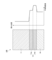
- FIG. 2 is a diagram showing a silicon carbide substrate 10A according to a first example of an embodiment.
- the left figure shows a cross-sectional view of the silicon carbide substrate 10A
- the right figure shows an impurity concentration profile of the silicon carbide substrate 10A.
- the silicon carbide substrate 10A mainly includes a silicon carbide single crystal substrate 50, a recombination promotion layer 19, and a drift region 11.
- Silicon carbide single crystal substrate 50 contains an n-type impurity such as nitrogen and has an n-type.
- the effective concentration of the n-type impurity in silicon carbide single crystal substrate 50 is, for example, not less than 1 ⁇ 10 18 cm ⁇ 3 and not more than 7 ⁇ 10 18 cm ⁇ 3 .
- the recombination promotion layer 19 is provided on a silicon carbide single crystal substrate 50.
- the recombination promotion layer 19 has a first region 19a, a second region 19b, and a third region 19c.
- the first region 19a is provided on the second region 19b.
- the first region 19a is in contact with the drift region 11.
- the first region 19a contains an n-type impurity such as nitrogen or phosphorus, and has an n-type.
- the effective concentration of the n-type impurity in the first region 19a is higher than the effective concentration of the n-type impurity in the silicon carbide single crystal substrate 50.
- the effective concentration of the n-type impurity in the first region 19a is, for example, not less than 5 ⁇ 10 18 cm ⁇ 3 and not more than 2 ⁇ 10 19 cm ⁇ 3 .
- the second region 19b is provided on the third region 19c.
- the second region 19b is provided at a position separated from the upper surface of the recombination promotion layer 19.
- the second region 19b is provided between the first region 19a and the third region 19c.
- the second region 19b contains n-type impurities such as nitrogen or phosphorus and has an n-type.
- the effective concentration of the n-type impurity in the second region 19b is higher than the effective concentration of the n-type impurity in the first region 19a.
- the effective concentration of the n-type impurity in the second region 19b is, for example, 1 ⁇ 10 19 cm ⁇ 3 or more.
- the third region 19c is provided on the silicon carbide single crystal substrate 50.
- the third region 19c is in contact with the silicon carbide single crystal substrate 50.
- the third region 19c contains an n-type impurity such as nitrogen or phosphorus and has an n-type.
- the effective concentration of the n-type impurity in the third region 19c is, for example, the same as the effective concentration of the n-type impurity in the first region 19a. In this case, the third region 19c has a lower concentration than the second region 19b. Therefore, the lattice mismatch with the silicon carbide single crystal substrate 50 is reduced, and thus defect generation can be suppressed.
- the effective concentration of the n-type impurity in the third region 19c is, for example, 5 ⁇ 10 18 cm ⁇ 3 or more and 2 ⁇ 10 19 cm ⁇ 3 or less.
- the drift region 11 is provided on the recombination promotion layer 19.
- the drift region 11 is in contact with the first region 19a.
- the drift region 11 contains n-type impurities such as nitrogen or phosphorus and has an n-type.
- the effective concentration of the n-type impurity in the drift region 11 is, for example, not less than 1 ⁇ 10 14 cm ⁇ 3 and not more than 5 ⁇ 10 16 cm ⁇ 3 .
- the recombination promotion layer 19 has a first region 19a and a second region 19b.
- the first region 19a is provided on the second region 19b.
- the effective concentration of n-type impurities in the second region 19b is higher than the effective concentration of n-type impurities in the first region 19a.
- the impurity concentration in the outermost region (first region 19a) of the recombination promotion layer 19 is low, stacking faults are unlikely to be formed in the outermost surface of the recombination promotion layer 19. Therefore, stacking faults are prevented from being inherited from the recombination promotion layer 19 to the drift region 11.
- second region 19b since a region (second region 19b) with a high impurity concentration exists in the recombination promotion layer 19, the recombination of carriers is promoted. Therefore, the recombination efficiency is improved and the required thickness of the recombination promotion layer 19 can be reduced. Reducing the required thickness of the recombination promotion layer 19 shortens the time required for epitaxial growth when forming the recombination promotion layer 19, thereby reducing manufacturing costs.
- a silicon carbide single crystal substrate 50 is prepared.
- the silicon carbide single crystal substrate 50 contains n-type impurities such as nitrogen and has an n-type.
- the recombination promotion layer 19 is formed on the silicon carbide single crystal substrate 50. Specifically, the recombination promotion layer 19 is formed on the silicon carbide single crystal substrate 50 by epitaxial growth with the addition of n-type impurities such as nitrogen or phosphorus. Next, ions are implanted into the recombination promotion layer 19. A second region 19b is formed at a position separated from the upper surface of the recombination promotion layer 19 by the ion implantation. As the second region 19b is formed, a first region 19a is formed on the second region 19b of the recombination promotion layer 19, and a third region 19c is formed below the second region 19b of the recombination promotion layer 19. In the ion implantation to form the second region 19b, for example, an n-type impurity such as nitrogen or phosphorus is implanted.
- a silicon carbide epitaxial layer 40 is formed on the recombination promotion layer 19.
- the silicon carbide epitaxial layer 40 can be formed by epitaxial growth with the addition of an n-type impurity such as nitrogen.
- ions are implanted into the silicon carbide epitaxial layer 40.
- the body region 12, the source region 13, and the contact region 18 are formed by ion implantation.
- the remaining portion of the silicon carbide epitaxial layer 40 functions as the drift region 11.
- a p-type impurity such as aluminum is ion implanted.
- an n-type impurity such as phosphorus is ion implanted.
- a silicon carbide substrate 10A can be manufactured in which a recombination promotion layer 19 and a silicon carbide epitaxial layer 40 are formed in this order on a silicon carbide single crystal substrate 50.
- the second region 19b is formed at a position separated from the upper surface of the recombination promotion layer 19 by ion implantation into the recombination promotion layer 19.
- the first region 19a is formed on the second region 19b of the recombination promotion layer 19.
- the effective concentration of the n-type impurity in the second region 19b is higher than the effective concentration of the n-type impurity in the first region 19a.
- the impurity concentration in the outermost region (first region 19a) of the recombination promotion layer 19 is low, stacking faults are unlikely to be formed on the outermost surface of the recombination promotion layer 19. Therefore, the transfer of stacking faults from the recombination promotion layer 19 to the drift region 11 is suppressed.
- the recombination of carriers is promoted. This improves recombination efficiency and reduces the required thickness of the recombination promotion layer 19. Reducing the required thickness of the recombination promotion layer 19 shortens the time required for epitaxial growth when forming the recombination promotion layer 19, thereby reducing manufacturing costs.
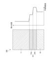
- FIG. 3 is a diagram showing a silicon carbide substrate 10B according to a second example of an embodiment.
- the left figure shows a cross-sectional view of the silicon carbide substrate 10B
- the right figure shows an impurity concentration profile of the silicon carbide substrate 10B.
- Silicon carbide substrate 10B differs from silicon carbide substrate 10A in that recombination promotion layer 19 does not have third region 19c, but has first region 19a and second region 19b.
- the rest of the configuration of silicon carbide substrate 10B is the same as, for example, silicon carbide substrate 10A. The following description will focus on the configuration that differs from silicon carbide substrate 10A.
- the recombination promotion layer 19 has a first region 19a and a second region 19b.
- the first region 19a is provided on the second region 19b.
- the first region 19a contacts the drift region 11.
- the second region 19b is provided on the silicon carbide single crystal substrate 50.
- the second region 19b is provided at a position spaced apart from the upper surface of the recombination promotion layer 19.
- the second region 19b contacts the silicon carbide single crystal substrate 50.
- the recombination promotion layer 19 has a first region 19a and a second region 19b.
- the first region 19a is provided on the second region 19b.
- the effective concentration of n-type impurities in the second region 19b is higher than the effective concentration of n-type impurities in the first region 19a.
- the same effects as those of the silicon carbide substrate 10A and the silicon carbide semiconductor device 100 having the silicon carbide substrate 10A can be obtained.
- Silicon carbide substrate 10B can be manufactured, for example, by a method similar to that for silicon carbide substrate 10A.
- the method for manufacturing silicon carbide substrate 10B provides the same effects as the method for manufacturing silicon carbide substrate 10A.
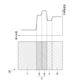
- FIG. 4 is a diagram showing a silicon carbide substrate 10C according to a third example of an embodiment.
- the left figure shows a cross-sectional view of the silicon carbide substrate 10C
- the right figure shows an impurity concentration profile of the silicon carbide substrate 10C.
- the silicon carbide substrate 10C mainly includes a silicon carbide single crystal substrate 50, a buffer layer 20, and a drift region 11.
- the buffer layer 20 is provided on a silicon carbide single crystal substrate 50.
- the buffer layer 20 has a fourth region 20a, a fifth region 20b, and a sixth region 20c.
- the fourth region 20a is provided on the fifth region 20b.
- the fourth region 20a contacts the drift region 11.
- the fourth region 20a contains an n-type impurity such as nitrogen or phosphorus, and has an n-type.
- the effective concentration of the n-type impurity in the fourth region 20a is lower than the effective concentration of the n-type impurity in the silicon carbide single crystal substrate 50.
- the effective concentration of the n-type impurity in the fourth region 20a is, for example, 2 ⁇ 10 17 cm ⁇ 3 or more and 3 ⁇ 10 18 cm ⁇ 3 or less.
- the effective concentration of the n-type impurity in the fourth region 20a is approximately constant, and the effective concentration of the n-type impurity at the interface between the fourth region 20a and the drift region 11 may be abruptly switched from the concentration in the fourth region 20a to the concentration in the drift region 11. In this case, the resistance of the silicon carbide semiconductor device 100 is unlikely to be high. In contrast, when the effective concentration of n-type impurities in fourth region 20a continuously decreases toward drift region 11, the resistance of silicon carbide semiconductor device 100 is likely to increase.
- the fifth region 20b is provided on the sixth region 20c.
- the fifth region 20b is provided at a position separated from the upper surface of the buffer layer 20.
- the fifth region 20b is provided between the fourth region 20a and the sixth region 20c.
- the fifth region 20b contains an n-type impurity such as nitrogen or phosphorus, and has an n-type.
- the effective concentration of the n-type impurity in the fifth region 20b is higher than the effective concentration of the n-type impurity in the silicon carbide single crystal substrate 50.
- the effective concentration of the n-type impurity in the fifth region 20b is, for example, 1 ⁇ 10 19 cm ⁇ 3 or more.
- the sixth region 20c is provided on the silicon carbide single crystal substrate 50.
- the sixth region 20c is in contact with the silicon carbide single crystal substrate 50.
- the sixth region 20c contains n-type impurities such as nitrogen or phosphorus, and has an n-type.
- the effective concentration of the n-type impurities in the sixth region 20c is, for example, the same as the effective concentration of the n-type impurities in the fourth region 20a. In this case, the sixth region 20c has a lower concentration than the fifth region 20b. Therefore, the lattice mismatch with the silicon carbide single crystal substrate 50 is reduced, and thus defect generation can be suppressed.
- the effective concentration of the n-type impurities in the sixth region 20c is, for example, 2 ⁇ 10 17 cm ⁇ 3 or more and 3 ⁇ 10 18 cm ⁇ 3 or less.
- the drift region 11 is provided on the buffer layer 20.
- the drift region 11 is in contact with the fourth region 20a.
- the drift region 11 contains an n-type impurity such as nitrogen or phosphorus and has an n-type.
- the effective concentration of the n-type impurity in the drift region 11 is, for example, not less than 1 ⁇ 10 14 cm ⁇ 3 and not more than 5 ⁇ 10 16 cm ⁇ 3 .
- the buffer layer 20 has a fourth region 20a and a fifth region 20b.
- the fourth region 20a is provided on the fifth region 20b.
- the effective concentration of n-type impurities in the fifth region 20b is higher than the effective concentration of n-type impurities in the fourth region 20a.
- the impurity concentration in the outermost region (fourth region 20a) of the buffer layer 20 is low, stacking faults are unlikely to be formed in the outermost surface of the buffer layer 20. Therefore, stacking faults are prevented from being inherited from the buffer layer 20 to the drift region 11.
- the buffer layer 20 since a region (fifth region 20b) with a high impurity concentration exists in the buffer layer 20, carrier recombination is promoted. Therefore, the recombination efficiency is improved and the required thickness of the buffer layer 20 can be reduced. Reducing the required thickness of the buffer layer 20 shortens the time required for epitaxial growth when forming the buffer layer 20, thereby reducing manufacturing costs.
- a silicon carbide single crystal substrate 50 is prepared.
- the silicon carbide single crystal substrate 50 contains n-type impurities such as nitrogen and has an n-type.
- the buffer layer 20 is formed on the silicon carbide single crystal substrate 50.
- the buffer layer 20 is formed on the silicon carbide single crystal substrate 50 by epitaxial growth with the addition of n-type impurities such as nitrogen or phosphorus.
- ions are implanted into the buffer layer 20.
- a fifth region 20b is formed at a position separated from the upper surface of the buffer layer 20 by the ion implantation. With the formation of the fifth region 20b, a fourth region 20a is formed on the fifth region 20b of the buffer layer 20, and a sixth region 20c is formed below the fifth region 20b of the buffer layer 20.
- an n-type impurity such as nitrogen or phosphorus is implanted.
- a silicon carbide epitaxial layer 40 is formed on the buffer layer 20.
- the method for forming the silicon carbide epitaxial layer 40 may be the same as the method for forming the silicon carbide epitaxial layer 40 in the method for manufacturing the silicon carbide substrate 10A.
- a silicon carbide substrate 10C can be manufactured in which a buffer layer 20 and a silicon carbide epitaxial layer 40 are formed in this order on a silicon carbide single crystal substrate 50.
- the fifth region 20b is formed at a position separated from the upper surface of the buffer layer 20 by ion implantation into the buffer layer 20.
- the fourth region 20a is formed on the fifth region 20b of the buffer layer 20.
- the effective concentration of n-type impurities in the fifth region 20b is higher than the effective concentration of n-type impurities in the fourth region 20a. In this case, since the impurity concentration in the outermost region (fourth region 20a) of the buffer layer 20 is low, stacking faults are unlikely to be formed in the outermost surface of the buffer layer 20.
- FIG. 5 is a diagram showing a silicon carbide substrate 10D according to a fourth embodiment.
- the left figure shows a cross-sectional view of the silicon carbide substrate 10D
- the right figure shows an impurity concentration profile of the silicon carbide substrate 10D.
- Silicon carbide substrate 10D differs from silicon carbide substrate 10C in that buffer layer 20 does not have sixth region 20c, but has fourth region 20a and fifth region 20b.
- Other configurations of silicon carbide substrate 10D are the same as, for example, silicon carbide substrate 10C. The following description will focus on the configurations that differ from silicon carbide substrate 10C.
- the buffer layer 20 has a fourth region 20a and a fifth region 20b.
- the fourth region 20a is provided on the fifth region 20b.
- the fourth region 20a contacts the drift region 11.
- the fifth region 20b is provided on the silicon carbide single crystal substrate 50.
- the fifth region 20b is provided at a position spaced apart from the upper surface of the recombination promotion layer 19.
- the fifth region 20b contacts the silicon carbide single crystal substrate 50.
- the buffer layer 20 has a fourth region 20a and a fifth region 20b.
- the fourth region 20a is provided on the fifth region 20b.
- the effective concentration of n-type impurities in the fifth region 20b is higher than the effective concentration of n-type impurities in the fourth region 20a. In this case, the same effects as those of the silicon carbide substrate 10C and the silicon carbide semiconductor device 100 having the silicon carbide substrate 10C can be obtained.
- Silicon carbide substrate 10D can be manufactured, for example, by a method similar to that for silicon carbide substrate 10C.
- the method for manufacturing silicon carbide substrate 10D provides the same effects as the method for manufacturing silicon carbide substrate 10C.
- FIG. 6 is a diagram showing a silicon carbide substrate 10E according to a fifth embodiment.
- the left figure shows a cross-sectional view of the silicon carbide substrate 10E
- the right figure shows an impurity concentration profile of the silicon carbide substrate 10E.
- Silicon carbide substrate 10E differs from silicon carbide substrate 10A in that it has a buffer layer 21 between silicon carbide single crystal substrate 50 and recombination promotion layer 19.
- the rest of the configuration of silicon carbide substrate 10E is the same as, for example, silicon carbide substrate 10A. Below, the configuration that differs from silicon carbide substrate 10A will be mainly described.
- the silicon carbide substrate 10E mainly includes a silicon carbide single crystal substrate 50, a buffer layer 21, a recombination promotion layer 19, and a drift region 11.
- the buffer layer 21 is provided on the silicon carbide single crystal substrate 50.
- the buffer layer 21 is provided between the silicon carbide single crystal substrate 50 and the recombination promotion layer 19.
- the buffer layer 21 contains an n-type impurity such as nitrogen or phosphorus, and has an n-type.
- the effective concentration of the n-type impurity in the buffer layer 21 is lower than the effective concentration of the n-type impurity in the silicon carbide single crystal substrate 50.
- the effective concentration of the n-type impurity in the buffer layer 21 is, for example, not less than 2 ⁇ 10 17 cm ⁇ 3 and not more than 3 ⁇ 10 18 cm ⁇ 3 .
- the recombination promotion layer 19 has a first region 19a and a second region 19b.
- the first region 19a is provided on the second region 19b.
- the effective concentration of n-type impurities in the second region 19b is higher than the effective concentration of n-type impurities in the first region 19a.
- the same effects as those of the silicon carbide substrate 10A and the silicon carbide semiconductor device 100 having the silicon carbide substrate 10A can be obtained.
- the buffer layer 21 is provided between the silicon carbide single crystal substrate 50 and the recombination promotion layer 19.
- the basal plane dislocations present in the silicon carbide single crystal substrate 50 are easily converted to threading edge dislocations at the interface between the silicon carbide single crystal substrate 50 and the buffer layer 21. Therefore, the basal plane dislocations can be prevented from reaching the drift region 11.
- the expansion of stacking faults in the drift region 11 is prevented when a current is applied in the forward direction to the pn junction, and as a result, the increase in the on-voltage can be prevented.
- a silicon carbide single crystal substrate 50 is prepared.
- the silicon carbide single crystal substrate 50 contains n-type impurities such as nitrogen and has an n-type.
- a buffer layer 21 is formed on the silicon carbide single crystal substrate 50.
- the buffer layer 21 is formed on the silicon carbide single crystal substrate 50 by epitaxial growth with the addition of n-type impurities such as nitrogen or phosphorus.
- the recombination promotion layer 19 is formed on the buffer layer 21.
- the method for forming the recombination promotion layer 19 may be the same as the method for forming the recombination promotion layer 19 in the manufacturing method of the silicon carbide substrate 10A.
- a silicon carbide epitaxial layer 40 is formed on the recombination promotion layer 19.
- the method for forming the silicon carbide epitaxial layer 40 may be the same as the method for forming the silicon carbide epitaxial layer 40 in the method for manufacturing the silicon carbide substrate 10A.
- a silicon carbide substrate 10E can be manufactured in which a buffer layer 21 and a silicon carbide epitaxial layer 40 are formed in this order on a silicon carbide single crystal substrate 50.
- the second region 19b is formed at a position separated from the upper surface of the recombination promotion layer 19 by ion implantation into the recombination promotion layer 19.
- the first region 19a is formed on the second region 19b of the recombination promotion layer 19.
- the effective concentration of the n-type impurity in the second region 19b is higher than the effective concentration of the n-type impurity in the first region 19a. In this case, the same effects as those of the silicon carbide substrate 10A and the silicon carbide semiconductor device 100 having the silicon carbide substrate 10A can be obtained.
- buffer layer 21 is grown by epitaxial growth on silicon carbide single crystal substrate 50
- basal plane dislocations present in silicon carbide single crystal substrate 50 are likely to be converted to threading edge dislocations at the interface between silicon carbide single crystal substrate 50 and buffer layer 21. Therefore, basal plane dislocations can be prevented from reaching drift region 11.
- the expansion of stacking faults in drift region 11 when forward current is applied to the pn junction is prevented, and as a result, an increase in on-voltage can be prevented.
- FIG. 7 is a diagram showing a silicon carbide substrate 10F according to a sixth embodiment.
- the left diagram shows a cross-sectional view of the silicon carbide substrate 10F
- the right diagram shows an impurity concentration profile of the silicon carbide substrate 10F.
- Silicon carbide substrate 10F differs from silicon carbide substrate 10E in that recombination promotion layer 19 does not have third region 19c, but has first region 19a and second region 19b.
- the rest of the configuration of silicon carbide substrate 10F is the same as, for example, silicon carbide substrate 10E. The following description will focus on the configuration that differs from silicon carbide substrate 10E.
- the recombination promotion layer 19 has a first region 19a and a second region 19b.
- the first region 19a is provided on the second region 19b.
- the first region 19a contacts the drift region 11.
- the second region 19b is provided on the silicon carbide single crystal substrate 50.
- the second region 19b is provided at a position spaced apart from the upper surface of the recombination promotion layer 19.
- the second region 19b contacts the silicon carbide single crystal substrate 50.
- the recombination promotion layer 19 has a first region 19a and a second region 19b.
- the first region 19a is provided on the second region 19b.
- the effective concentration of n-type impurities in the second region 19b is higher than the effective concentration of n-type impurities in the first region 19a.
- the same effects as those of the silicon carbide substrate 10E and the silicon carbide semiconductor device 100 having the silicon carbide substrate 10E can be obtained.
- Silicon carbide substrate 10F can be manufactured, for example, by a method similar to that for silicon carbide substrate 10E.
- the manufacturing method for silicon carbide substrate 10F provides the same effects as the manufacturing method for silicon carbide substrate 10E.
- the effective concentration of p-type impurities and the effective concentration of n-type impurities in each of the above impurity regions can be measured using a scanning capacitance microscope (SCM) method or a secondary ion mass spectrometry (SIMS) method, for example.
- SCM scanning capacitance microscope
- SIMS secondary ion mass spectrometry
- Silicon carbide substrate 10A Silicon carbide substrate 10B Silicon carbide substrate 10C Silicon carbide substrate 10D Silicon carbide substrate 10E Silicon carbide substrate 10F Silicon carbide substrate 11 Drift region 12 Body region 13 Source region 18 Contact region 19 Recombination promotion layer 19a First region 19b Second region 19c Third region 20 Buffer layer 20a Fourth region 20b Fifth region 20c Sixth region 21 Buffer layer 40 Silicon carbide epitaxial layer 50 Silicon carbide single crystal substrate 60 Source electrode 61 Contact electrode 62 Source wiring 70 Drain electrode 81 Gate insulating film 82 Gate electrode 83 Interlayer insulating film 90 Contact hole 100 Silicon carbide semiconductor device
Landscapes
- Recrystallisation Techniques (AREA)
- Crystals, And After-Treatments Of Crystals (AREA)
Abstract
Description
本開示は、炭化珪素基板、炭化珪素半導体装置および炭化珪素基板の製造方法に関する。 This disclosure relates to a silicon carbide substrate, a silicon carbide semiconductor device, and a method for manufacturing a silicon carbide substrate.
本出願は、2023年6月8日出願の日本出願第2023-094793号に基づく優先権を主張し、前記日本出願に記載された全ての記載内容を援用するものである。 This application claims priority to Japanese Application No. 2023-094793, filed on June 8, 2023, and incorporates all of the contents of said Japanese application by reference.
炭化珪素単結晶基板と炭化珪素エピタキシャル層との間に、炭化珪素単結晶基板よりも不純物濃度が高い再結合促進層(炭化珪素エピタキシャル層)を設けた炭化珪素エピタキシャル基板が開示されている。炭化珪素エピタキシャル層が設けられることで、炭化珪素単結晶基板に含まれる基底面転移からの積層欠陥の発生が抑制される。 A silicon carbide epitaxial substrate is disclosed in which a recombination-promoting layer (silicon carbide epitaxial layer) having a higher impurity concentration than the silicon carbide single crystal substrate is provided between the silicon carbide single crystal substrate and the silicon carbide epitaxial layer. The provision of the silicon carbide epitaxial layer suppresses the occurrence of stacking faults due to basal plane dislocations contained in the silicon carbide single crystal substrate.
本開示の炭化珪素基板は、第1導電型を有する炭化珪素単結晶基板と、前記炭化珪素単結晶基板の上に設けられ、前記第1導電型を有する炭化珪素エピタキシャル層と、前記炭化珪素エピタキシャル層の上に設けられ、前記第1導電型を有するドリフト層と、を有し、前記炭化珪素エピタキシャル層は、第1領域と、第2領域とを有し、前記第1領域は、前記第2領域の上に位置し、前記第1領域の不純物濃度は、前記炭化珪素単結晶基板の不純物濃度よりも高く、前記第2領域の不純物濃度は、前記第1領域の不純物濃度よりも高い。 The silicon carbide substrate of the present disclosure comprises a silicon carbide single crystal substrate having a first conductivity type, a silicon carbide epitaxial layer having the first conductivity type provided on the silicon carbide single crystal substrate, and a drift layer having the first conductivity type provided on the silicon carbide epitaxial layer, the silicon carbide epitaxial layer having a first region and a second region, the first region being located on the second region, the impurity concentration of the first region being higher than the impurity concentration of the silicon carbide single crystal substrate, and the impurity concentration of the second region being higher than the impurity concentration of the first region.
[本開示が解決しようとする課題]
炭化珪素エピタキシャル層を薄くする場合、炭化珪素エピタキシャル層の不純物濃度を高くすることが有効である。しかしながら、炭化珪素エピタキシャル層の不純物濃度を高くすると、結晶歪みにより炭化珪素エピタキシャル層に積層欠陥が形成されやすい。積層欠陥が形成されると、炭化珪素エピタキシャル層の上に形成されるドリフト層にも積層欠陥が拡張する。
[Problem to be solved by the present disclosure]
In order to make the silicon carbide epitaxial layer thinner, it is effective to increase the impurity concentration of the silicon carbide epitaxial layer. However, when the impurity concentration of the silicon carbide epitaxial layer is increased, stacking faults are likely to be formed in the silicon carbide epitaxial layer due to crystal distortion. When stacking faults are formed, the stacking faults also extend to the drift layer formed on the silicon carbide epitaxial layer.
本開示は、再結合効率を向上し、必要な炭化珪素エピタキシャル層の厚みを低減できる炭化珪素基板、炭化珪素半導体装置および炭化珪素半導体装置の製造方法を提供することを目的とする。 The present disclosure aims to provide a silicon carbide substrate, a silicon carbide semiconductor device, and a method for manufacturing a silicon carbide semiconductor device that can improve recombination efficiency and reduce the required thickness of a silicon carbide epitaxial layer.
[本開示の効果]
本開示によれば、再結合効率を向上し、必要な炭化珪素エピタキシャル層の厚みを低減できる炭化珪素基板、炭化珪素半導体装置および炭化珪素半導体装置の製造方法を提供できる。
[Effects of the present disclosure]
Advantageous Effects of Invention The present disclosure can provide a silicon carbide substrate, a silicon carbide semiconductor device, and a method for manufacturing a silicon carbide semiconductor device that can improve recombination efficiency and reduce the required thickness of a silicon carbide epitaxial layer.
実施するための形態について、以下に説明する。 The form for implementation is explained below.
[本開示の実施形態の説明]
最初に本開示の実施態様を列記して説明する。以下の説明では、同一または対応する要素には同一の符号を付し、それらについて同じ説明は繰り返さない。
[Description of the embodiments of the present disclosure]
First, the embodiments of the present disclosure will be described. In the following description, the same or corresponding elements are denoted by the same reference numerals, and the same description thereof will not be repeated.
〔1〕 本開示の一態様に係る炭化珪素基板は、第1導電型を有する炭化珪素単結晶基板と、前記炭化珪素単結晶基板の上に設けられ、前記第1導電型を有する炭化珪素エピタキシャル層と、前記炭化珪素エピタキシャル層の上に設けられ、前記第1導電型を有するドリフト層と、を有し、前記炭化珪素エピタキシャル層は、第1領域と、第2領域とを有し、前記第1領域は、前記第2領域の上に位置し、前記第1領域の不純物濃度は、前記炭化珪素単結晶基板の不純物濃度よりも高く、前記第2領域の不純物濃度は、前記第1領域の不純物濃度よりも高い。この場合、炭化珪素エピタキシャル層の最表面の不純物濃度が低いので、炭化珪素エピタキシャル層の最表面において積層欠陥が形成されにくい。そのため、炭化珪素エピタキシャル層からドリフト層に積層欠陥が引き継がれることが抑制される。また、炭化珪素エピタキシャル層内に不純物濃度が高い領域が存在するので、キャリアの再結合が促進される。そのため、再結合効率を向上し、必要な炭化珪素エピタキシャル層の厚みを低減できる。 [1] A silicon carbide substrate according to one embodiment of the present disclosure includes a silicon carbide single crystal substrate having a first conductivity type, a silicon carbide epitaxial layer having the first conductivity type provided on the silicon carbide single crystal substrate, and a drift layer having the first conductivity type provided on the silicon carbide epitaxial layer, the silicon carbide epitaxial layer having a first region and a second region, the first region being located on the second region, the impurity concentration of the first region being higher than the impurity concentration of the silicon carbide single crystal substrate, and the impurity concentration of the second region being higher than the impurity concentration of the first region. In this case, since the impurity concentration of the outermost surface of the silicon carbide epitaxial layer is low, stacking faults are unlikely to be formed on the outermost surface of the silicon carbide epitaxial layer. Therefore, stacking faults are prevented from being inherited from the silicon carbide epitaxial layer to the drift layer. In addition, since there are regions with high impurity concentrations in the silicon carbide epitaxial layer, carrier recombination is promoted. This improves recombination efficiency and reduces the required thickness of the silicon carbide epitaxial layer.
〔2〕 〔1〕において、前記炭化珪素エピタキシャル層は、前記炭化珪素単結晶基板と前記第2領域との間に設けられる第3領域を有し、前記第3領域の不純物濃度は、前記第1領域の不純物濃度と同じであってもよい。この場合、第2領域よりもより低濃度の第3領域により炭化珪素単結晶基板との格子不整合が小さくなるため欠陥生成を抑制できる。 [2] In [1], the silicon carbide epitaxial layer may have a third region provided between the silicon carbide single crystal substrate and the second region, and the impurity concentration of the third region may be the same as the impurity concentration of the first region. In this case, the third region has a lower concentration than the second region, which reduces the lattice mismatch with the silicon carbide single crystal substrate, thereby suppressing the generation of defects.
〔3〕 〔1〕または〔2〕において、前記炭化珪素単結晶基板と前記炭化珪素エピタキシャル層との間に設けられ、前記第1導電型を有するバッファ層を有し、前記バッファ層の不純物濃度は、前記炭化珪素単結晶基板の不純物濃度よりも低くてもよい。この場合、炭化珪素単結晶基板の上にエピタキシャル成長によりバッファ層を成長させる際に、炭化珪素単結晶基板内に存在する基底面転移(BPD:Basal Plane Dislocation)が炭化珪素単結晶基板とバッファ層との界面で貫通刃状転移(TED:Threading Edge Dislocation)に転換されやすい。そのため、基底面転移がドリフト層に到達することを抑制できる。その結果、pn接合に順方向通電を行った際にドリフト層に積層欠陥が拡大することが抑制され、結果としてオン電圧の上昇を抑制できる。 [3] In [1] or [2], a buffer layer having the first conductivity type may be provided between the silicon carbide single crystal substrate and the silicon carbide epitaxial layer, and the impurity concentration of the buffer layer may be lower than the impurity concentration of the silicon carbide single crystal substrate. In this case, when the buffer layer is grown by epitaxial growth on the silicon carbide single crystal substrate, basal plane dislocations (BPDs) present in the silicon carbide single crystal substrate are likely to be converted to threading edge dislocations (TEDs) at the interface between the silicon carbide single crystal substrate and the buffer layer. Therefore, the basal plane dislocations can be prevented from reaching the drift layer. As a result, the expansion of stacking faults in the drift layer when a forward current is applied to the pn junction is prevented, and as a result, an increase in the on-voltage can be prevented.
〔4〕 本開示の他の一態様に係る炭化珪素基板は、第1導電型を有する炭化珪素単結晶基板と、前記炭化珪素単結晶基板の上に設けられ、前記第1導電型を有するバッファ層と、前記バッファ層の上に設けられ、前記第1導電型を有するドリフト層と、を有し、前記バッファ層は、第4領域と、第5領域とを有し、前記第4領域は、前記第5領域の上に位置し、前記第4領域の不純物濃度は、前記炭化珪素単結晶基板の不純物濃度よりも低く、前記第5領域の不純物濃度は、前記炭化珪素単結晶基板の不純物濃度よりも高い。この場合、バッファ層の最表面の不純物濃度が低いので、バッファ層の最表面において積層欠陥が形成されにくい。そのため、バッファ層からドリフト層に積層欠陥が引き継がれることが抑制される。また、バッファ層内に不純物濃度が高い領域が存在するので、キャリアの再結合が促進される。そのため、再結合効率を向上し、必要なバッファ層の厚みを低減できる。 [4] A silicon carbide substrate according to another embodiment of the present disclosure includes a silicon carbide single crystal substrate having a first conductivity type, a buffer layer having the first conductivity type provided on the silicon carbide single crystal substrate, and a drift layer having the first conductivity type provided on the buffer layer, the buffer layer having a fourth region and a fifth region, the fourth region being located on the fifth region, the impurity concentration of the fourth region being lower than the impurity concentration of the silicon carbide single crystal substrate, and the impurity concentration of the fifth region being higher than the impurity concentration of the silicon carbide single crystal substrate. In this case, since the impurity concentration of the outermost surface of the buffer layer is low, stacking faults are unlikely to be formed on the outermost surface of the buffer layer. Therefore, stacking faults are prevented from being inherited from the buffer layer to the drift layer. In addition, since a region with a high impurity concentration exists in the buffer layer, carrier recombination is promoted. Therefore, the recombination efficiency is improved and the required thickness of the buffer layer can be reduced.
〔5〕 〔4〕において、前記バッファ層は、前記炭化珪素単結晶基板と前記第5領域との間に設けられる第6領域を有し、前記第6領域の不純物濃度は、前記第4領域の不純物濃度と同じであってもよい。この場合、第5領域よりもより低濃度の第6領域により炭化珪素単結晶基板との格子不整合が小さくなるため欠陥生成を抑制できる。 [5] In [4], the buffer layer may have a sixth region provided between the silicon carbide single crystal substrate and the fifth region, and the impurity concentration of the sixth region may be the same as the impurity concentration of the fourth region. In this case, the sixth region has a lower concentration than the fifth region, which reduces the lattice mismatch with the silicon carbide single crystal substrate, thereby suppressing the generation of defects.
〔6〕 本開示の他の一態様に係る炭化珪素半導体装置は、第1主面と、前記第1主面と反対の第2主面とを有する炭化珪素基板を備え、前記炭化珪素基板は、第1導電型を有する炭化珪素単結晶基板と、前記炭化珪素単結晶基板の上に設けられ、前記第1導電型を有する炭化珪素エピタキシャル層と、前記炭化珪素エピタキシャル層の上に設けられ、前記第1導電型を有するドリフト層と、を有し、前記炭化珪素エピタキシャル層は、第1領域と、第2領域とを有し、前記第1領域は、前記第2領域の上に位置し、前記第1領域の不純物濃度は、前記炭化珪素単結晶基板の不純物濃度よりも高く、前記第2領域の不純物濃度は、前記第1領域の不純物濃度よりも高い。この場合、炭化珪素エピタキシャル層の最表面の不純物濃度が低いので、炭化珪素エピタキシャル層の最表面において積層欠陥が形成されにくい。そのため、炭化珪素エピタキシャル層からドリフト層に積層欠陥が引き継がれることが抑制される。また、炭化珪素エピタキシャル層内に不純物濃度が高い領域が存在するので、キャリアの再結合が促進される。そのため、再結合効率を向上し、必要な炭化珪素エピタキシャル層の厚みを低減できる。 [6] A silicon carbide semiconductor device according to another aspect of the present disclosure comprises a silicon carbide substrate having a first main surface and a second main surface opposite to the first main surface, the silicon carbide substrate having a silicon carbide single crystal substrate having a first conductivity type, a silicon carbide epitaxial layer having the first conductivity type provided on the silicon carbide single crystal substrate, and a drift layer having the first conductivity type provided on the silicon carbide epitaxial layer, the silicon carbide epitaxial layer having a first region and a second region, the first region being located on the second region, the impurity concentration of the first region being higher than the impurity concentration of the silicon carbide single crystal substrate, and the impurity concentration of the second region being higher than the impurity concentration of the first region. In this case, since the impurity concentration of the outermost surface of the silicon carbide epitaxial layer is low, stacking faults are unlikely to form on the outermost surface of the silicon carbide epitaxial layer. This prevents stacking faults from being inherited from the silicon carbide epitaxial layer to the drift layer. In addition, the presence of a region with a high impurity concentration in the silicon carbide epitaxial layer promotes carrier recombination. This improves recombination efficiency and reduces the required thickness of the silicon carbide epitaxial layer.
〔7〕 本開示の他の一態様に係る炭化珪素半導体装置は、第1主面と、前記第1主面と反対の第2主面とを有する炭化珪素基板を備え、前記炭化珪素基板は、第1導電型を有する炭化珪素単結晶基板と、前記炭化珪素単結晶基板の上に設けられ、前記第1導電型を有するバッファ層と、前記バッファ層の上に設けられ、前記第1導電型を有するドリフト層と、を有し、前記バッファ層は、第4領域と、第5領域とを有し、前記第4領域は、前記第5領域の上に位置し、前記第4領域の不純物濃度は、前記炭化珪素単結晶基板の不純物濃度よりも低く、前記第5領域の不純物濃度は、前記炭化珪素単結晶基板の不純物濃度よりも高い。この場合、バッファ層の最表面の不純物濃度が低いので、バッファ層の最表面において積層欠陥が形成されにくい。そのため、バッファ層からドリフト層に積層欠陥が引き継がれることが抑制される。また、バッファ層内に不純物濃度が高い領域が存在するので、キャリアの再結合が促進される。そのため、再結合効率を向上し、必要なバッファ層の厚みを低減できる。 [7] A silicon carbide semiconductor device according to another aspect of the present disclosure includes a silicon carbide substrate having a first main surface and a second main surface opposite to the first main surface, the silicon carbide substrate having a silicon carbide single crystal substrate having a first conductivity type, a buffer layer having the first conductivity type provided on the silicon carbide single crystal substrate, and a drift layer having the first conductivity type provided on the buffer layer, the buffer layer having a fourth region and a fifth region, the fourth region being located on the fifth region, the impurity concentration of the fourth region being lower than the impurity concentration of the silicon carbide single crystal substrate, and the impurity concentration of the fifth region being higher than the impurity concentration of the silicon carbide single crystal substrate. In this case, since the impurity concentration of the outermost surface of the buffer layer is low, stacking faults are unlikely to be formed on the outermost surface of the buffer layer. Therefore, stacking faults are suppressed from being inherited from the buffer layer to the drift layer. In addition, since a region with a high impurity concentration exists in the buffer layer, carrier recombination is promoted. This improves recombination efficiency and reduces the required thickness of the buffer layer.
〔8〕本開示の他の一態様に係る炭化珪素基板の製造方法は、第1導電型を有する炭化珪素単結晶基板の上に、前記第1導電型を有し、前記炭化珪素単結晶基板よりも不純物濃度が高い炭化珪素エピタキシャル層を形成する工程と、前記炭化珪素エピタキシャル層へのイオン注入により、前記炭化珪素エピタキシャル層の上面から離隔した位置に前記第1導電型を有する第2領域を形成する工程と、前記第2領域を形成する工程の後、前記炭化珪素エピタキシャル層の上に、前記第1導電型を有するドリフト層を形成する工程と、を有し、前記第2領域の形成に伴って、前記炭化珪素エピタキシャル層の前記第2領域の上に第1領域が形成され、前記第1領域の不純物濃度は、前記炭化珪素単結晶基板の不純物濃度よりも高く、前記第2領域の不純物濃度は、前記第1領域の不純物濃度よりも高い。この場合、炭化珪素エピタキシャル層の最表面の不純物濃度が低いので、炭化珪素エピタキシャル層の最表面において積層欠陥が形成されにくい。そのため、炭化珪素エピタキシャル層からドリフト層に積層欠陥が引き継がれることが抑制される。また、炭化珪素エピタキシャル層内に不純物濃度が高い領域が存在するので、キャリアの再結合が促進される。そのため、再結合効率を向上し、必要な炭化珪素エピタキシャル層の厚みを低減できる。 [8] A method for manufacturing a silicon carbide substrate according to another aspect of the present disclosure includes the steps of: forming a silicon carbide epitaxial layer having a first conductivity type and having a higher impurity concentration than the silicon carbide single crystal substrate on a silicon carbide single crystal substrate having the first conductivity type; forming a second region having the first conductivity type at a position spaced from an upper surface of the silicon carbide epitaxial layer by ion implantation into the silicon carbide epitaxial layer; and, after the step of forming the second region, forming a drift layer having the first conductivity type on the silicon carbide epitaxial layer, wherein a first region is formed on the second region of the silicon carbide epitaxial layer in conjunction with the formation of the second region, and the impurity concentration of the first region is higher than the impurity concentration of the silicon carbide single crystal substrate and the impurity concentration of the second region is higher than the impurity concentration of the first region. In this case, since the impurity concentration at the outermost surface of the silicon carbide epitaxial layer is low, stacking faults are unlikely to form at the outermost surface of the silicon carbide epitaxial layer. This prevents stacking faults from being inherited from the silicon carbide epitaxial layer to the drift layer. In addition, since there is a region with a high impurity concentration in the silicon carbide epitaxial layer, carrier recombination is promoted. This improves recombination efficiency and reduces the required thickness of the silicon carbide epitaxial layer.
〔9〕本開示の他の一態様に係る炭化珪素基板の製造方法は、第1導電型を有する炭化珪素単結晶基板の上に、前記第1導電型を有し、前記炭化珪素単結晶基板よりも不純物濃度が低いバッファ層を形成する工程と、前記バッファ層へのイオン注入により、前記バッファ層の上面から離隔した位置に前記第1導電型を有する第5領域を形成する工程と、前記第5領域を形成する工程の後、前記バッファ層の上に、前記第1導電型を有するドリフト層を形成する工程と、を有し、前記第5領域の形成に伴って、前記バッファ層の前記第5領域の上に第4領域が形成され、前記第4領域の不純物濃度は、前記炭化珪素単結晶基板の不純物濃度よりも低く、前記第5領域の不純物濃度は、前記炭化珪素単結晶基板の不純物濃度よりも高い。この場合、バッファ層の最表面の不純物濃度が低いので、バッファ層の最表面において積層欠陥が形成されにくい。そのため、バッファ層からドリフト層に積層欠陥が引き継がれることが抑制される。また、バッファ層内に不純物濃度が高い領域が存在するので、キャリアの再結合が促進される。そのため、再結合効率を向上し、必要なバッファ層の厚みを低減できる。 [9] A method for manufacturing a silicon carbide substrate according to another aspect of the present disclosure includes the steps of forming a buffer layer having a first conductivity type and a lower impurity concentration than the silicon carbide single crystal substrate on a silicon carbide single crystal substrate having a first conductivity type, forming a fifth region having the first conductivity type at a position separated from the upper surface of the buffer layer by ion implantation into the buffer layer, and forming a drift layer having the first conductivity type on the buffer layer after the step of forming the fifth region, and a fourth region is formed on the fifth region of the buffer layer with the formation of the fifth region, and the impurity concentration of the fourth region is lower than the impurity concentration of the silicon carbide single crystal substrate, and the impurity concentration of the fifth region is higher than the impurity concentration of the silicon carbide single crystal substrate. In this case, since the impurity concentration of the outermost surface of the buffer layer is low, stacking faults are unlikely to be formed on the outermost surface of the buffer layer. Therefore, stacking faults are suppressed from being inherited from the buffer layer to the drift layer. In addition, since a region having a high impurity concentration exists in the buffer layer, recombination of carriers is promoted. This improves recombination efficiency and reduces the required thickness of the buffer layer.
[本開示の実施形態の詳細]
以下、本開示の実施形態について詳細に説明するが、本開示はこれらに限定されるものではない。
[Details of the embodiment of the present disclosure]
Hereinafter, embodiments of the present disclosure will be described in detail, but the present disclosure is not limited thereto.
(炭化珪素半導体装置)
実施形態に係る炭化珪素半導体装置100について説明する。図1は、実施形態に係る炭化珪素半導体装置100を示す断面図である。
(Silicon carbide semiconductor device)
DETAILED DESCRIPTION OF THE PREFERRED EMBODIMENTS A silicon
炭化珪素半導体装置100は、炭化珪素基板10と、ゲート絶縁膜81と、ゲート電極82と、層間絶縁膜83と、ソース電極60と、ドレイン電極70とを主に有する。
The silicon
炭化珪素基板10は、炭化珪素単結晶基板50と、炭化珪素単結晶基板50上にある炭化珪素エピタキシャル層40とを含む。炭化珪素基板10は、第1主面1と、第1主面1と反対の第2主面2とを有する。炭化珪素エピタキシャル層40は第1主面1を構成し、炭化珪素単結晶基板50は第2主面2を構成する。炭化珪素単結晶基板50および炭化珪素エピタキシャル層40は、例えばポリタイプ4Hの六方晶炭化珪素から構成されている。炭化珪素単結晶基板50は、例えば窒素(N)などのn型不純物を含みn型を有する。炭化珪素基板10に半導体素子が形成されている。
The
実施形態では、炭化珪素基板10に半導体素子の一例として電界効果トランジスタが形成されている。炭化珪素エピタキシャル層40は、ドリフト領域11と、ボディ領域12と、ソース領域13と、コンタクト領域18と、再結合促進層19とを主に有する。
In the embodiment, a field effect transistor is formed as an example of a semiconductor element on the
ドリフト領域11は、例えば窒素またはリン(P)などのn型不純物を含み、n型を有する。
The
ボディ領域12は、ドリフト領域11上に設けられている。ボディ領域12は、例えばアルミニウム(Al)などのp型不純物を含み、p型を有する。
The
ソース領域13は、ボディ領域12によってドリフト領域11から隔てられるようにボディ領域12上に設けられている。ソース領域13は、例えば窒素またはリンなどのn型不純物を含み、n型を有する。ソース領域13は、第1主面1を構成する。
The
コンタクト領域18は、例えばアルミニウムなどのp型不純物を含み、p型を有する。コンタクト領域18は、第1主面1を構成する。コンタクト領域18は、ソース領域13を貫通し、ボディ領域12と接する。
The
再結合促進層19は、炭化珪素単結晶基板50の上に設けられている。再結合促進層19は、炭化珪素単結晶基板50とドリフト領域11との間に設けられている。再結合促進層19の詳細については後述する。
The
第1主面1には、複数のゲートトレンチ5が設けられている。ゲートトレンチ5は、例えば第1主面1に平行な第1方向に延びており、複数のゲートトレンチ5が第2方向に並んでいる。ゲートトレンチ5は、ドリフト領域11からなる底面4を有する。底面4は、例えば第2主面2と平行な平面である。ゲートトレンチ5は、ソース領域13およびボディ領域12を貫通して底面4に連なる側面3を有する。側面3は、底面4を含む平面に対して傾斜する。
A plurality of
ゲート絶縁膜81は、側面3および底面4に接する。ゲート絶縁膜81は、例えば酸化膜である。ゲート絶縁膜81は、例えば二酸化珪素を含む材料により構成されている。ゲート絶縁膜81は、底面4においてドリフト領域11と接する。ゲート絶縁膜81は、側面3においてソース領域13、ボディ領域12およびドリフト領域11の各々と接する。ゲート絶縁膜81は、第1主面1においてソース領域13と接してもよい。
The
ゲート電極82は、ゲート絶縁膜81上に設けられている。ゲート電極82は、例えば導電性不純物を含むポリシリコンから構成されている。ゲート電極82は、ゲートトレンチ5の内部に配置されている。
The
層間絶縁膜83は、ゲート電極82およびゲート絶縁膜81と接する。層間絶縁膜83は、例えば二酸化珪素を含む材料から構成されている。層間絶縁膜83およびゲート絶縁膜81には、第2方向に一定の間隔でコンタクトホール90が形成されている。コンタクトホール90は、第2方向で隣り合うコンタクトホール90の間にゲートトレンチ5が位置するように設けられている。コンタクトホール90は、第1方向に延びる。コンタクトホール90を通じて、ソース領域13およびコンタクト領域18が層間絶縁膜83およびゲート絶縁膜81から露出する。
The
ソース電極60は、第1主面1と接する。ソース電極60は、コンタクト電極61と、ソース配線62とを有する。
The source electrode 60 contacts the first
コンタクト電極61は、コンタクトホール90内に設けられている。コンタクト電極61は、第1主面1において、ソース領域13およびコンタクト領域18と接する。コンタクト電極61は、チタン(Ti)、アルミニウム(Al)および珪素(Si)を含む材料から構成されている。コンタクト電極61は、ソース領域13およびコンタクト領域18とオーミック接合する。コンタクト電極61は、コンタクトホール90を通じて炭化珪素基板10に接続されている。
The
ソース配線62は、アルミニウムまたは銅(Cu)を含む材料から構成されている。ソース配線62は、アルミニウムおよび銅を含む材料から構成されていてもよい。ソース電極60は、層間絶縁膜83によりゲート電極82から電気的に絶縁されている。ソース電極60が、ソース配線62と層間絶縁膜83との間に窒化チタン(TiN)膜などのバリアメタル膜を含んでもよい。
The
ドレイン電極70は、第2主面2と接する。ドレイン電極70は、第2主面2において炭化珪素単結晶基板50と接する。ドレイン電極70は、ドリフト領域11と電気的に接続されている。ドレイン電極70は、コンタクト電極61と同じ材料により構成されている。ドレイン電極70は、炭化珪素単結晶基板50とオーミック接合する。
The
(炭化珪素基板)
次に、実施形態に係る炭化珪素半導体装置100が有する炭化珪素基板10について説明する。
(Silicon carbide substrate)
Next,
図2を参照し、実施形態の第1例に係る炭化珪素基板10Aについて説明する。図2は、実施形態の第1例に係る炭化珪素基板10Aを示す図である。図2において、左図に炭化珪素基板10Aの断面図を示し、右図に炭化珪素基板10Aの不純物濃度プロファイルを示す。
With reference to FIG. 2, a
炭化珪素基板10Aは、炭化珪素単結晶基板50と、再結合促進層19と、ドリフト領域11とを主に有する。
The
炭化珪素単結晶基板50は、例えば窒素などのn型不純物を含み、n型を有する。炭化珪素単結晶基板50のn型不純物の実効濃度は、例えば1×1018cm-3以上7×1018cm-3以下である。
Silicon carbide
再結合促進層19は、炭化珪素単結晶基板50の上に設けられている。再結合促進層19は、第1領域19aと、第2領域19bと、第3領域19cとを有する。
The
第1領域19aは、第2領域19bの上に設けられている。第1領域19aは、ドリフト領域11と接する。第1領域19aは、例えば窒素またはリンなどのn型不純物を含み、n型を有する。第1領域19aのn型不純物の実効濃度は、炭化珪素単結晶基板50のn型不純物の実効濃度よりも高い。第1領域19aのn型不純物の実効濃度は、例えば5×1018cm-3以上2×1019cm-3以下である。
The
第2領域19bは、第3領域19cの上に設けられている。第2領域19bは、再結合促進層19の上面から離隔した位置に設けられている。第2領域19bは、第1領域19aと第3領域19cとの間に設けられている。第2領域19bは、例えば窒素またはリンなどのn型不純物を含み、n型を有する。第2領域19bのn型不純物の実効濃度は、第1領域19aのn型不純物の実効濃度よりも高い。第2領域19bのn型不純物の実効濃度は、例えば1×1019cm-3以上である。
The
第3領域19cは、炭化珪素単結晶基板50の上に設けられている。第3領域19cは、炭化珪素単結晶基板50と接する。第3領域19cは、例えば窒素またはリンなどのn型不純物を含み、n型を有する。第3領域19cのn型不純物の実効濃度は、例えば第1領域19aのn型不純物の実効濃度と同じである。この場合、第3領域19cは第2領域19bと比較して低濃度である。そのため、炭化珪素単結晶基板50との格子不整合が小さくなるため欠陥生成を抑制できる。第3領域19cのn型不純物の実効濃度は、例えば5×1018cm-3以上2×1019cm-3以下である。
The
ドリフト領域11は、再結合促進層19の上に設けられている。ドリフト領域11は、第1領域19aと接する。ドリフト領域11は、例えば窒素またはリンなどのn型不純物を含み、n型を有する。ドリフト領域11のn型不純物の実効濃度は、例えば1×1014cm-3以上5×1016cm-3以下である。
The
以上に説明した炭化珪素基板10A、および炭化珪素基板10Aを有する炭化珪素半導体装置100によれば、再結合促進層19が、第1領域19aと、第2領域19bとを有する。第1領域19aは、第2領域19bの上に設けられている。第2領域19bのn型不純物の実効濃度は、第1領域19aのn型不純物の実効濃度よりも高い。この場合、再結合促進層19の最表面の領域(第1領域19a)の不純物濃度が低いので、再結合促進層19の最表面において積層欠陥が形成されにくい。そのため、再結合促進層19からドリフト領域11に積層欠陥が引き継がれることが抑制される。また、再結合促進層19内に不純物濃度が高い領域(第2領域19b)が存在するので、キャリアの再結合が促進される。そのため、再結合効率を向上し、必要な再結合促進層19の厚みを低減できる。必要な再結合促進層19の厚みが低減されると、再結合促進層19を形成する際のエピタキシャル成長に要する時間が短縮され、製造コストが低減される。
According to the
次に、炭化珪素基板10Aの製造方法について説明する。
Next, a method for manufacturing
まず、炭化珪素単結晶基板50を準備する。例えば、炭化珪素単結晶基板50は、窒素などのn型不純物を含み、n型を有する。
First, a silicon carbide
次に、炭化珪素単結晶基板50の上に再結合促進層19を形成する。具体的には、炭化珪素単結晶基板50の上に、窒素またはリンなどのn型不純物を添加したエピタキシャル成長により、再結合促進層19を形成する。次に、再結合促進層19へのイオン注入を行う。イオン注入により、再結合促進層19の上面から離隔した位置に第2領域19bが形成される。第2領域19bの形成に伴って、再結合促進層19の第2領域19bの上に第1領域19aが形成され、再結合促進層19の第2領域19bの下に第3領域19cが形成される。第2領域19bを形成するためのイオン注入においては、例えば窒素またはリンなどのn型不純物を注入する。
Next, the
次に、再結合促進層19の上に炭化珪素エピタキシャル層40を形成する。例えば、炭化珪素エピタキシャル層40は、窒素などのn型不純物を添加したエピタキシャル成長により形成できる。
Next, a silicon
次に、炭化珪素エピタキシャル層40へのイオン注入を行う。例えば、イオン注入により、ボディ領域12、ソース領域13およびコンタクト領域18が形成される。炭化珪素エピタキシャル層40の残部がドリフト領域11として機能する。ボディ領域12またはコンタクト領域18を形成するためのイオン注入においては、例えばアルミニウムなどのp型不純物をイオン注入する。ソース領域13を形成するためのイオン注入においては、例えばリンなどのn型不純物をイオン注入する。
Next, ions are implanted into the silicon
以上により、炭化珪素単結晶基板50の上に、再結合促進層19および炭化珪素エピタキシャル層40がこの順番で形成された炭化珪素基板10Aを製造できる。
By the above steps, a
以上に説明した炭化珪素基板10Aの製造方法によれば、炭化珪素単結晶基板50の上に再結合促進層19を形成した後に、再結合促進層19へのイオン注入により、再結合促進層19の上面から離隔した位置に第2領域19bを形成する。第2領域19bの形成に伴って、再結合促進層19の第2領域19bの上に第1領域19aが形成される。第2領域19bのn型不純物の実効濃度は、第1領域19aのn型不純物の実効濃度よりも高い。この場合、再結合促進層19の最表面の領域(第1領域19a)の不純物濃度が低いので、再結合促進層19の最表面において積層欠陥が形成されにくい。そのため、再結合促進層19からドリフト領域11に積層欠陥が引き継がれることが抑制される。また、再結合促進層19内に不純物濃度が高い領域(第2領域19b)が存在するので、キャリアの再結合が促進される。そのため、再結合効率を向上し、必要な再結合促進層19の厚みを低減できる。必要な再結合促進層19の厚みが低減されると、再結合促進層19を形成する際のエピタキシャル成長に要する時間が短縮され、製造コストが低減される。
According to the manufacturing method of the
図3を参照し、実施形態の第2例に係る炭化珪素基板10Bについて説明する。図3は、実施形態の第2例に係る炭化珪素基板10Bを示す図である。図3において、左図に炭化珪素基板10Bの断面図を示し、右図に炭化珪素基板10Bの不純物濃度プロファイルを示す。
With reference to FIG. 3, a
炭化珪素基板10Bは、再結合促進層19が、第3領域19cを有しておらず、第1領域19aと、第2領域19bとを有する構成において、炭化珪素基板10Aと異なる。炭化珪素基板10Bのその他の構成は、例えば炭化珪素基板10Aと同じである。以下、炭化珪素基板10Aと異なる構成を中心に説明する。
再結合促進層19は、第1領域19aと、第2領域19bとを有する。第1領域19aは、第2領域19bの上に設けられている。第1領域19aは、ドリフト領域11と接する。第2領域19bは、炭化珪素単結晶基板50の上に設けられている。第2領域19bは、再結合促進層19の上面から離隔した位置に設けられている。第2領域19bは、炭化珪素単結晶基板50と接する。
The
以上に説明した炭化珪素基板10B、および炭化珪素基板10Bを有する炭化珪素半導体装置100によれば、再結合促進層19が、第1領域19aと、第2領域19bとを有する。第1領域19aは、第2領域19bの上に設けられている。第2領域19bのn型不純物の実効濃度は、第1領域19aのn型不純物の実効濃度よりも高い。この場合、炭化珪素基板10A、および炭化珪素基板10Aを有する炭化珪素半導体装置100と同様の効果が得られる。
According to the
炭化珪素基板10Bは、例えば炭化珪素基板10Aと同様の方法で製造できる。炭化珪素基板10Bの製造方法によれば、炭化珪素基板10Aの製造方法と同様の効果が得られる。
図4を参照し、実施形態の第3例に係る炭化珪素基板10Cについて説明する。図4は、実施形態の第3例に係る炭化珪素基板10Cを示す図である。図4において、左図に炭化珪素基板10Cの断面図を示し、右図に炭化珪素基板10Cの不純物濃度プロファイルを示す。
With reference to FIG. 4, a
炭化珪素基板10Cは、再結合促進層19に代えて、バッファ層20を有する構成において、炭化珪素基板10Aと異なる。炭化珪素基板10Cのその他の構成は、例えば炭化珪素基板10Aと同じである。以下、炭化珪素基板10Aと異なる構成を中心に説明する。
炭化珪素基板10Cは、炭化珪素単結晶基板50と、バッファ層20と、ドリフト領域11とを主に有する。
The
バッファ層20は、炭化珪素単結晶基板50の上に設けられている。バッファ層20は、第4領域20aと、第5領域20bと、第6領域20cとを有する。
The
第4領域20aは、第5領域20bの上に設けられている。第4領域20aは、ドリフト領域11と接する。第4領域20aは、例えば窒素またはリンなどのn型不純物を含み、n型を有する。第4領域20aのn型不純物の実効濃度は、炭化珪素単結晶基板50のn型不純物の実効濃度よりも低い。第4領域20aのn型不純物の実効濃度は、例えば2×1017cm-3以上3×1018cm-3以下である。第4領域20aのn型不純物の実効濃度は略一定であり、第4領域20aとドリフト領域11との界面においてn型不純物の実効濃度が第4領域20aの濃度からドリフト領域11の濃度に急峻に切り替わってよい。この場合、炭化珪素半導体装置100の抵抗が高くなりにくい。これに対し、第4領域20aのn型不純物の実効濃度がドリフト領域11に向かって連続的に低くなる場合、炭化珪素半導体装置100の抵抗が高くなりやすい。
The
第5領域20bは、第6領域20cの上に設けられている。第5領域20bは、バッファ層20の上面から離隔した位置に設けられている。第5領域20bは、第4領域20aと第6領域20cとの間に設けられている。第5領域20bは、例えば窒素またはリンなどのn型不純物を含み、n型を有する。第5領域20bのn型不純物の実効濃度は、炭化珪素単結晶基板50のn型不純物の実効濃度よりも高い。第5領域20bのn型不純物の実効濃度は、例えば1×1019cm-3以上である。
The
第6領域20cは、炭化珪素単結晶基板50の上に設けられている。第6領域20cは、炭化珪素単結晶基板50と接する。第6領域20cは、例えば窒素またはリンなどのn型不純物を含み、n型を有する。第6領域20cのn型不純物の実効濃度は、例えば第4領域20aのn型不純物の実効濃度と同じである。この場合、第6領域20cは第5領域20bと比較して低濃度である。そのため、炭化珪素単結晶基板50との格子不整合が小さくなるため欠陥生成を抑制できる。第6領域20cのn型不純物の実効濃度は、例えば2×1017cm-3以上3×1018cm-3以下である。
The
ドリフト領域11は、バッファ層20の上に設けられている。ドリフト領域11は、第4領域20aと接する。ドリフト領域11は、例えば窒素またはリンなどのn型不純物を含み、n型を有する。ドリフト領域11のn型不純物の実効濃度は、例えば1×1014cm-3以上5×1016cm-3以下である。
The
以上に説明した炭化珪素基板10C、および炭化珪素基板10Cを有する炭化珪素半導体装置100によれば、バッファ層20が、第4領域20aと、第5領域20bとを有する。第4領域20aは、第5領域20bの上に設けられている。第5領域20bのn型不純物の実効濃度は、第4領域20aのn型不純物の実効濃度よりも高い。この場合、バッファ層20の最表面の領域(第4領域20a)の不純物濃度が低いので、バッファ層20の最表面において積層欠陥が形成されにくい。そのため、バッファ層20からドリフト領域11に積層欠陥が引き継がれることが抑制される。また、バッファ層20内に不純物濃度が高い領域(第5領域20b)が存在するので、キャリアの再結合が促進される。そのため、再結合効率を向上し、必要なバッファ層20の厚みを低減できる。必要なバッファ層20の厚みが低減されると、バッファ層20を形成する際のエピタキシャル成長に要する時間が短縮され、製造コストが低減される。
According to the
次に、炭化珪素基板10Cの製造方法について説明する。
Next, a method for manufacturing the
まず、炭化珪素単結晶基板50を準備する。例えば、炭化珪素単結晶基板50は、窒素などのn型不純物を含み、n型を有する。
First, a silicon carbide
次に、炭化珪素単結晶基板50の上にバッファ層20を形成する。具体的には、炭化珪素単結晶基板50の上に、窒素またはリンなどのn型不純物を添加したエピタキシャル成長により、バッファ層20を形成する。次に、バッファ層20へのイオン注入を行う。イオン注入により、バッファ層20の上面から離隔した位置に第5領域20bが形成される。第5領域20bの形成に伴って、バッファ層20の第5領域20bの上に第4領域20aが形成され、バッファ層20の第5領域20bの下に第6領域20cが形成される。第5領域20bを形成するためのイオン注入においては、例えば窒素またはリンなどのn型不純物を注入する。
Next, the
次に、バッファ層20の上に炭化珪素エピタキシャル層40を形成する。炭化珪素エピタキシャル層40を形成する方法は、炭化珪素基板10Aの製造方法において炭化珪素エピタキシャル層40を形成する方法と同様であってよい。
Next, a silicon
以上により、炭化珪素単結晶基板50の上に、バッファ層20および炭化珪素エピタキシャル層40がこの順番で形成された炭化珪素基板10Cを製造できる。
By the above steps, a
以上に説明した炭化珪素基板10Cの製造方法によれば、炭化珪素単結晶基板50の上にバッファ層20を形成した後に、バッファ層20へのイオン注入により、バッファ層20の上面から離隔した位置に第5領域20bを形成する。第5領域20bの形成に伴って、バッファ層20の第5領域20bの上に第4領域20aが形成される。第5領域20bのn型不純物の実効濃度は、第4領域20aのn型不純物の実効濃度よりも高い。この場合、バッファ層20の最表面の領域(第4領域20a)の不純物濃度が低いので、バッファ層20の最表面において積層欠陥が形成されにくい。そのため、バッファ層20からドリフト領域11に積層欠陥が引き継がれることが抑制される。また、バッファ層20内に不純物濃度が高い領域(第5領域20b)が存在するので、キャリアの再結合が促進される。そのため、再結合効率を向上し、必要なバッファ層20の厚みを低減できる。必要なバッファ層20の厚みが低減されると、バッファ層20を形成する際のエピタキシャル成長に要する時間が短縮され、製造コストが低減される。
According to the manufacturing method of the
図5を参照し、実施形態の第4例に係る炭化珪素基板10Dについて説明する。図5は、実施形態の第4例に係る炭化珪素基板10Dを示す図である。図5において、左図に炭化珪素基板10Dの断面図を示し、右図に炭化珪素基板10Dの不純物濃度プロファイルを示す。
With reference to FIG. 5, a
炭化珪素基板10Dは、バッファ層20が、第6領域20cを有しておらず、第4領域20aと、第5領域20bとを有する構成において、炭化珪素基板10Cと異なる。炭化珪素基板10Dのその他の構成は、例えば炭化珪素基板10Cと同じである。以下、炭化珪素基板10Cと異なる構成を中心に説明する。
バッファ層20は、第4領域20aと、第5領域20bとを有する。第4領域20aは、第5領域20bの上に設けられている。第4領域20aは、ドリフト領域11と接する。第5領域20bは、炭化珪素単結晶基板50の上に設けられている。第5領域20bは、再結合促進層19の上面から離隔した位置に設けられている。第5領域20bは、炭化珪素単結晶基板50と接する。
The
以上に説明した炭化珪素基板10D、および炭化珪素基板10Dを有する炭化珪素半導体装置100によれば、バッファ層20が、第4領域20aと、第5領域20bとを有する。第4領域20aは、第5領域20bの上に設けられている。第5領域20bのn型不純物の実効濃度は、第4領域20aのn型不純物の実効濃度よりも高い。この場合、炭化珪素基板10C、および炭化珪素基板10Cを有する炭化珪素半導体装置100と同様の効果が得られる。
According to the
炭化珪素基板10Dは、例えば炭化珪素基板10Cと同様の方法で製造できる。炭化珪素基板10Dの製造方法によれば、炭化珪素基板10Cの製造方法と同様の効果が得られる。
図6を参照し、実施形態の第5例に係る炭化珪素基板10Eについて説明する。図6は、実施形態の第5例に係る炭化珪素基板10Eを示す図である。図6において、左図に炭化珪素基板10Eの断面図を示し、右図に炭化珪素基板10Eの不純物濃度プロファイルを示す。
With reference to FIG. 6, a
炭化珪素基板10Eは、炭化珪素単結晶基板50と再結合促進層19との間にバッファ層21を有する構成において、炭化珪素基板10Aと異なる。炭化珪素基板10Eのその他の構成は、例えば炭化珪素基板10Aと同じである。以下、炭化珪素基板10Aと異なる構成を中心に説明する。
炭化珪素基板10Eは、炭化珪素単結晶基板50と、バッファ層21と、再結合促進層19と、ドリフト領域11とを主に有する。
The
バッファ層21は、炭化珪素単結晶基板50の上に設けられている。バッファ層21は、炭化珪素単結晶基板50と再結合促進層19との間に設けられている。バッファ層21は、例えば窒素またはリンなどのn型不純物を含み、n型を有する。バッファ層21のn型不純物の実効濃度は、炭化珪素単結晶基板50のn型不純物の実効濃度よりも低い。バッファ層21のn型不純物の実効濃度は、例えば2×1017cm-3以上3×1018cm-3以下である。
The
以上に説明した炭化珪素基板10E、および炭化珪素基板10Eを有する炭化珪素半導体装置100によれば、再結合促進層19が、第1領域19aと、第2領域19bとを有する。第1領域19aは、第2領域19bの上に設けられている。第2領域19bのn型不純物の実効濃度は、第1領域19aのn型不純物の実効濃度よりも高い。この場合、炭化珪素基板10A、および炭化珪素基板10Aを有する炭化珪素半導体装置100と同様の効果が得られる。
According to the
また、炭化珪素基板10E、および炭化珪素基板10Eを有する炭化珪素半導体装置100によれば、炭化珪素単結晶基板50と再結合促進層19との間にバッファ層21を有する。この場合、炭化珪素単結晶基板50の上にエピタキシャル成長によりバッファ層21を成長させる際に、炭化珪素単結晶基板50内に存在する基底面転移が炭化珪素単結晶基板50とバッファ層21との界面で貫通刃状転移に転換されやすい。そのため、基底面転移がドリフト領域11に到達することを抑制できる。その結果、pn接合に順方向通電を行った際にドリフト領域11に積層欠陥が拡大することが抑制され、結果としてオン電圧の上昇を抑制できる。
Furthermore, according to the
次に、炭化珪素基板10Eの製造方法について説明する。
Next, a method for manufacturing the
まず、炭化珪素単結晶基板50を準備する。例えば、炭化珪素単結晶基板50は、窒素などのn型不純物を含み、n型を有する。
First, a silicon carbide
次に、炭化珪素単結晶基板50の上にバッファ層21を形成する。具体的には、炭化珪素単結晶基板50の上に、窒素またはリンなどのn型不純物を添加したエピタキシャル成長により、バッファ層21を形成する。
Next, a
次に、バッファ層21の上に再結合促進層19を形成する。再結合促進層19を形成する方法は、炭化珪素基板10Aの製造方法において再結合促進層19を形成する方法と同様であってよい。
Next, the
次に、再結合促進層19の上に炭化珪素エピタキシャル層40を形成する。炭化珪素エピタキシャル層40を形成する方法は、炭化珪素基板10Aの製造方法において炭化珪素エピタキシャル層40を形成する方法と同様であってよい。
Next, a silicon
以上により、炭化珪素単結晶基板50の上に、バッファ層21および炭化珪素エピタキシャル層40がこの順番で形成された炭化珪素基板10Eを製造できる。
By the above steps, a
以上に説明した炭化珪素基板10Eの製造方法によれば、炭化珪素単結晶基板50の上に再結合促進層19を形成した後に、再結合促進層19へのイオン注入により、再結合促進層19の上面から離隔した位置に第2領域19bを形成する。第2領域19bの形成に伴って、再結合促進層19の第2領域19bの上に第1領域19aが形成される。第2領域19bのn型不純物の実効濃度は、第1領域19aのn型不純物の実効濃度よりも高い。この場合、炭化珪素基板10A、および炭化珪素基板10Aを有する炭化珪素半導体装置100と同様の効果が得られる。
According to the manufacturing method of the
また、炭化珪素基板10Eの製造方法によれば、炭化珪素単結晶基板50の上にバッファ層21を形成した後に、バッファ層21の上に再結合促進層19を形成する。この場合、炭化珪素単結晶基板50の上にエピタキシャル成長によりバッファ層21を成長させる際に、炭化珪素単結晶基板50内に存在する基底面転移が炭化珪素単結晶基板50とバッファ層21との界面で貫通刃状転移に転換されやすい。そのため、基底面転移がドリフト領域11に到達することを抑制できる。その結果、pn接合に順方向通電を行った際にドリフト領域11に積層欠陥が拡大することが抑制され、結果としてオン電圧の上昇を抑制できる。
In addition, according to the manufacturing method of
図7を参照し、実施形態の第6例に係る炭化珪素基板10Fについて説明する。図7は、実施形態の第6例に係る炭化珪素基板10Fを示す図である。図7において、左図に炭化珪素基板10Fの断面図を示し、右図に炭化珪素基板10Fの不純物濃度プロファイルを示す。
With reference to FIG. 7, a
炭化珪素基板10Fは、再結合促進層19が、第3領域19cを有しておらず、第1領域19aと、第2領域19bとを有する構成において、炭化珪素基板10Eと異なる。炭化珪素基板10Fのその他の構成は、例えば炭化珪素基板10Eと同じである。以下、炭化珪素基板10Eと異なる構成を中心に説明する。
再結合促進層19は、第1領域19aと、第2領域19bとを有する。第1領域19aは、第2領域19bの上に設けられている。第1領域19aは、ドリフト領域11と接する。第2領域19bは、炭化珪素単結晶基板50の上に設けられている。第2領域19bは、再結合促進層19の上面から離隔した位置に設けられている。第2領域19bは、炭化珪素単結晶基板50と接する。
The
以上に説明した炭化珪素基板10F、および炭化珪素基板10Fを有する炭化珪素半導体装置100によれば、再結合促進層19が、第1領域19aと、第2領域19bとを有する。第1領域19aは、第2領域19bの上に設けられている。第2領域19bのn型不純物の実効濃度は、第1領域19aのn型不純物の実効濃度よりも高い。この場合、炭化珪素基板10E、および炭化珪素基板10Eを有する炭化珪素半導体装置100と同様の効果が得られる。
According to the
炭化珪素基板10Fは、例えば炭化珪素基板10Eと同様の方法で製造できる。炭化珪素基板10Fの製造方法によれば、炭化珪素基板10Eの製造方法と同様の効果が得られる。
上記の各不純物領域におけるp型不純物の実効濃度およびn型不純物の実効濃度は、走査型静電容量顕微鏡(SCM:Scanning Capacitance Microscope)法または二次イオン質量分析(SIMS:Secondary Ion Mass Spectrometry)法などにより測定可能である。 The effective concentration of p-type impurities and the effective concentration of n-type impurities in each of the above impurity regions can be measured using a scanning capacitance microscope (SCM) method or a secondary ion mass spectrometry (SIMS) method, for example.
以上、実施形態について詳述したが、特定の実施形態に限定されるものではなく、請求の範囲に記載された範囲内において、種々の変形および変更が可能である。 Although the embodiments have been described in detail above, the invention is not limited to specific embodiments, and various modifications and variations are possible within the scope of the claims.
1 第1主面
2 第2主面
3 側面
4 底面
5 ゲートトレンチ
10 炭化珪素基板
10A 炭化珪素基板
10B 炭化珪素基板
10C 炭化珪素基板
10D 炭化珪素基板
10E 炭化珪素基板
10F 炭化珪素基板
11 ドリフト領域
12 ボディ領域
13 ソース領域
18 コンタクト領域
19 再結合促進層
19a 第1領域
19b 第2領域
19c 第3領域
20 バッファ層
20a 第4領域
20b 第5領域
20c 第6領域
21 バッファ層
40 炭化珪素エピタキシャル層
50 炭化珪素単結晶基板
60 ソース電極
61 コンタクト電極
62 ソース配線
70 ドレイン電極
81 ゲート絶縁膜
82 ゲート電極
83 層間絶縁膜
90 コンタクトホール
100 炭化珪素半導体装置
1 First
Claims (9)
前記炭化珪素単結晶基板の上に設けられ、前記第1導電型を有する炭化珪素エピタキシャル層と、
前記炭化珪素エピタキシャル層の上に設けられ、前記第1導電型を有するドリフト層と、
を有し、
前記炭化珪素エピタキシャル層は、第1領域と、第2領域とを有し、
前記第1領域は、前記第2領域の上に位置し、
前記第1領域の不純物濃度は、前記炭化珪素単結晶基板の不純物濃度よりも高く、
前記第2領域の不純物濃度は、前記第1領域の不純物濃度よりも高い、
炭化珪素基板。 a silicon carbide single crystal substrate having a first conductivity type;
a silicon carbide epitaxial layer having the first conductivity type provided on the silicon carbide single crystal substrate;
a drift layer having the first conductivity type provided on the silicon carbide epitaxial layer;
having
the silicon carbide epitaxial layer has a first region and a second region;
the first region is located above the second region,
an impurity concentration of the first region is higher than an impurity concentration of the silicon carbide single crystal substrate;
The impurity concentration of the second region is higher than the impurity concentration of the first region.
Silicon carbide substrate.
前記第3領域の不純物濃度は、前記第1領域の不純物濃度と同じである、
請求項1に記載の炭化珪素基板。 the silicon carbide epitaxial layer has a third region provided between the silicon carbide single crystal substrate and the second region,
The impurity concentration of the third region is the same as the impurity concentration of the first region.
The silicon carbide substrate according to claim 1 .
前記バッファ層の不純物濃度は、前記炭化珪素単結晶基板の不純物濃度よりも低い、
請求項1または請求項2に記載の炭化珪素基板。 a buffer layer having the first conductivity type and provided between the silicon carbide single crystal substrate and the silicon carbide epitaxial layer;
an impurity concentration of the buffer layer is lower than an impurity concentration of the silicon carbide single crystal substrate;
The silicon carbide substrate according to claim 1 .
前記炭化珪素単結晶基板の上に設けられ、前記第1導電型を有するバッファ層と、
前記バッファ層の上に設けられ、前記第1導電型を有するドリフト層と、
を有し、
前記バッファ層は、第4領域と、第5領域とを有し、
前記第4領域は、前記第5領域の上に位置し、
前記第4領域の不純物濃度は、前記炭化珪素単結晶基板の不純物濃度よりも低く、
前記第5領域の不純物濃度は、前記炭化珪素単結晶基板の不純物濃度よりも高い、
炭化珪素基板。 a silicon carbide single crystal substrate having a first conductivity type;
a buffer layer having the first conductivity type provided on the silicon carbide single crystal substrate;
a drift layer having the first conductivity type provided on the buffer layer;
having
the buffer layer has a fourth region and a fifth region;
the fourth region is located above the fifth region,
an impurity concentration of the fourth region is lower than an impurity concentration of the silicon carbide single crystal substrate;
an impurity concentration of the fifth region is higher than an impurity concentration of the silicon carbide single crystal substrate;
Silicon carbide substrate.
前記第6領域の不純物濃度は、前記第4領域の不純物濃度と同じである、
請求項4に記載の炭化珪素基板。 the buffer layer has a sixth region provided between the silicon carbide single crystal substrate and the fifth region,
The impurity concentration of the sixth region is the same as the impurity concentration of the fourth region.
The silicon carbide substrate according to claim 4 .
前記炭化珪素基板は、
第1導電型を有する炭化珪素単結晶基板と、
前記炭化珪素単結晶基板の上に設けられ、前記第1導電型を有する炭化珪素エピタキシャル層と、
前記炭化珪素エピタキシャル層の上に設けられ、前記第1導電型を有するドリフト層と、
を有し、
前記炭化珪素エピタキシャル層は、第1領域と、第2領域とを有し、
前記第1領域は、前記第2領域の上に位置し、
前記第1領域の不純物濃度は、前記炭化珪素単結晶基板の不純物濃度よりも高く、
前記第2領域の不純物濃度は、前記第1領域の不純物濃度よりも高い、
炭化珪素半導体装置。 a silicon carbide substrate having a first main surface and a second main surface opposite the first main surface;
The silicon carbide substrate is
a silicon carbide single crystal substrate having a first conductivity type;
a silicon carbide epitaxial layer having the first conductivity type provided on the silicon carbide single crystal substrate;
a drift layer having the first conductivity type provided on the silicon carbide epitaxial layer;
having
the silicon carbide epitaxial layer has a first region and a second region;
the first region is located above the second region,
an impurity concentration of the first region is higher than an impurity concentration of the silicon carbide single crystal substrate;
The impurity concentration of the second region is higher than the impurity concentration of the first region.
Silicon carbide semiconductor devices.
前記炭化珪素基板は、
第1導電型を有する炭化珪素単結晶基板と、
前記炭化珪素単結晶基板の上に設けられ、前記第1導電型を有するバッファ層と、
前記バッファ層の上に設けられ、前記第1導電型を有するドリフト層と、
を有し、
前記バッファ層は、第4領域と、第5領域とを有し、
前記第4領域は、前記第5領域の上に位置し、
前記第4領域の不純物濃度は、前記炭化珪素単結晶基板の不純物濃度よりも低く、
前記第5領域の不純物濃度は、前記炭化珪素単結晶基板の不純物濃度よりも高い、
炭化珪素半導体装置。 a silicon carbide substrate having a first main surface and a second main surface opposite the first main surface;
The silicon carbide substrate is
a silicon carbide single crystal substrate having a first conductivity type;
a buffer layer having the first conductivity type provided on the silicon carbide single crystal substrate;
a drift layer having the first conductivity type provided on the buffer layer;
having
the buffer layer has a fourth region and a fifth region;
the fourth region is located above the fifth region,
an impurity concentration of the fourth region is lower than an impurity concentration of the silicon carbide single crystal substrate;
an impurity concentration of the fifth region is higher than an impurity concentration of the silicon carbide single crystal substrate;
Silicon carbide semiconductor devices.
前記炭化珪素エピタキシャル層へのイオン注入により、前記炭化珪素エピタキシャル層の上面から離隔した位置に前記第1導電型を有する第2領域を形成する工程と、
前記第2領域を形成する工程の後、前記炭化珪素エピタキシャル層の上に、前記第1導電型を有するドリフト層を形成する工程と、
を有し、
前記第2領域の形成に伴って、前記炭化珪素エピタキシャル層の前記第2領域の上に第1領域が形成され、
前記第1領域の不純物濃度は、前記炭化珪素単結晶基板の不純物濃度よりも高く、
前記第2領域の不純物濃度は、前記第1領域の不純物濃度よりも高い、
炭化珪素基板の製造方法。 forming a silicon carbide epitaxial layer having a first conductivity type on a silicon carbide single crystal substrate having the first conductivity type and having a higher impurity concentration than the silicon carbide single crystal substrate;
forming a second region having the first conductivity type at a position spaced from an upper surface of the silicon carbide epitaxial layer by ion implantation into the silicon carbide epitaxial layer;
forming a drift layer having the first conductivity type on the silicon carbide epitaxial layer after the step of forming the second region;
having
a first region is formed on the second region of the silicon carbide epitaxial layer in association with the formation of the second region;
an impurity concentration of the first region is higher than an impurity concentration of the silicon carbide single crystal substrate;
The impurity concentration of the second region is higher than the impurity concentration of the first region.
A method for manufacturing a silicon carbide substrate.
前記バッファ層へのイオン注入により、前記バッファ層の上面から離隔した位置に前記第1導電型を有する第5領域を形成する工程と、
前記第5領域を形成する工程の後、前記バッファ層の上に、前記第1導電型を有するドリフト層を形成する工程と、
を有し、
前記第5領域の形成に伴って、前記バッファ層の前記第5領域の上に第4領域が形成され、
前記第4領域の不純物濃度は、前記炭化珪素単結晶基板の不純物濃度よりも低く、
前記第5領域の不純物濃度は、前記炭化珪素単結晶基板の不純物濃度よりも高い、
炭化珪素基板の製造方法。 forming a buffer layer having a first conductivity type on a silicon carbide single crystal substrate having the first conductivity type and having an impurity concentration lower than that of the silicon carbide single crystal substrate;
forming a fifth region having the first conductivity type at a position spaced from an upper surface of the buffer layer by ion implantation into the buffer layer;
forming a drift layer having the first conductivity type on the buffer layer after the step of forming the fifth region;
having
a fourth region is formed on the fifth region of the buffer layer in association with the formation of the fifth region;
an impurity concentration of the fourth region is lower than an impurity concentration of the silicon carbide single crystal substrate;
an impurity concentration of the fifth region is higher than an impurity concentration of the silicon carbide single crystal substrate;
A method for manufacturing a silicon carbide substrate.
Priority Applications (3)
| Application Number | Priority Date | Filing Date | Title |
|---|---|---|---|
| JP2025525972A JPWO2024252795A1 (en) | 2023-06-08 | 2024-04-16 | |
| DE112024002456.4T DE112024002456T5 (en) | 2023-06-08 | 2024-04-16 | Silicon carbide substrate, silicon carbide semiconductor element and method for producing a silicon carbide substrate |
| CN202480025712.0A CN121014273A (en) | 2023-06-08 | 2024-04-16 | Silicon carbide substrate, silicon carbide semiconductor device, and method for manufacturing silicon carbide substrate |
Applications Claiming Priority (2)
| Application Number | Priority Date | Filing Date | Title |
|---|---|---|---|
| JP2023-094793 | 2023-06-08 | ||
| JP2023094793 | 2023-06-08 |
Publications (1)
| Publication Number | Publication Date |
|---|---|
| WO2024252795A1 true WO2024252795A1 (en) | 2024-12-12 |
Family
ID=93795382
Family Applications (1)
| Application Number | Title | Priority Date | Filing Date |
|---|---|---|---|
| PCT/JP2024/015148 Ceased WO2024252795A1 (en) | 2023-06-08 | 2024-04-16 | Silicon carbide substrate, silicon carbide semiconductor device, and method for manufacturing silicon carbide substrate |
Country Status (4)
| Country | Link |
|---|---|
| JP (1) | JPWO2024252795A1 (en) |
| CN (1) | CN121014273A (en) |
| DE (1) | DE112024002456T5 (en) |
| WO (1) | WO2024252795A1 (en) |
Citations (4)
| Publication number | Priority date | Publication date | Assignee | Title |
|---|---|---|---|---|
| WO2017094764A1 (en) * | 2015-12-02 | 2017-06-08 | 三菱電機株式会社 | Silicon carbide epitaxial substrate and silicon carbide semiconductor device |
| WO2018150861A1 (en) * | 2017-02-20 | 2018-08-23 | 日立金属株式会社 | Silicon carbide laminated substrate and production method therefor |
| WO2018207394A1 (en) * | 2017-05-10 | 2018-11-15 | 三菱電機株式会社 | Semiconductor device and manufacturing method thereof |
| JP2020141109A (en) * | 2019-03-01 | 2020-09-03 | 三菱電機株式会社 | SiC epitaxial wafer, semiconductor device, power conversion device |
Family Cites Families (1)
| Publication number | Priority date | Publication date | Assignee | Title |
|---|---|---|---|---|
| JP2023094793A (en) | 2021-12-24 | 2023-07-06 | 帝人ファーマ株式会社 | Method for supporting diagnosis of sleep apnea syndrome, apparatus for supporting diagnosis of sleep apnea syndrome, and kit for supporting diagnosis of sleep apnea syndrome |
-
2024
- 2024-04-16 DE DE112024002456.4T patent/DE112024002456T5/en active Pending
- 2024-04-16 CN CN202480025712.0A patent/CN121014273A/en active Pending
- 2024-04-16 JP JP2025525972A patent/JPWO2024252795A1/ja active Pending
- 2024-04-16 WO PCT/JP2024/015148 patent/WO2024252795A1/en not_active Ceased
Patent Citations (4)
| Publication number | Priority date | Publication date | Assignee | Title |
|---|---|---|---|---|
| WO2017094764A1 (en) * | 2015-12-02 | 2017-06-08 | 三菱電機株式会社 | Silicon carbide epitaxial substrate and silicon carbide semiconductor device |
| WO2018150861A1 (en) * | 2017-02-20 | 2018-08-23 | 日立金属株式会社 | Silicon carbide laminated substrate and production method therefor |
| WO2018207394A1 (en) * | 2017-05-10 | 2018-11-15 | 三菱電機株式会社 | Semiconductor device and manufacturing method thereof |
| JP2020141109A (en) * | 2019-03-01 | 2020-09-03 | 三菱電機株式会社 | SiC epitaxial wafer, semiconductor device, power conversion device |
Also Published As
| Publication number | Publication date |
|---|---|
| DE112024002456T5 (en) | 2026-03-26 |
| CN121014273A (en) | 2025-11-25 |
| JPWO2024252795A1 (en) | 2024-12-12 |
Similar Documents
| Publication | Publication Date | Title |
|---|---|---|
| US11978778B2 (en) | Semiconductor device | |
| CN102714143B (en) | Epitaxial wafer and semiconductor element | |
| JP5431667B2 (en) | Gallium nitride semiconductor device | |
| US7531889B2 (en) | Epitaxial substrate and semiconductor element | |
| JP7574892B2 (en) | Method for manufacturing silicon carbide semiconductor device | |
| JP2019140186A (en) | Semiconductor device, substrate, method for manufacturing semiconductor device, and method for manufacturing substrate | |
| US11177380B2 (en) | Silicon carbide semiconductor component | |
| JP2011140429A (en) | Epitaxial wafer and semiconductor element | |
| WO2024252795A1 (en) | Silicon carbide substrate, silicon carbide semiconductor device, and method for manufacturing silicon carbide substrate | |
| JP2009054659A (en) | Method for manufacturing gallium nitride semiconductor device | |
| JP2019140187A (en) | Semiconductor device, substrate, method for manufacturing semiconductor device, and method for manufacturing substrate | |
| US20220181504A1 (en) | Semiconductor device and production method for semiconductor device | |
| CN114678424A (en) | Silicon carbide MOSFET transistor device with improved characteristics and corresponding method of fabrication | |
| JP2021005736A (en) | Semiconductor device, substrate, method for manufacturing the semiconductor device, and method for manufacturing the substrate | |
| JP7601240B2 (en) | Silicon carbide semiconductor device and silicon carbide semiconductor substrate | |
| KR20190127324A (en) | Semiconductor device and method manufacturing the same | |
| KR20120029703A (en) | A nitride semiconductor device and a method of fabricating thereof |
Legal Events
| Date | Code | Title | Description |
|---|---|---|---|
| 121 | Ep: the epo has been informed by wipo that ep was designated in this application |
Ref document number: 24819033 Country of ref document: EP Kind code of ref document: A1 |
|
| ENP | Entry into the national phase |
Ref document number: 2025525972 Country of ref document: JP Kind code of ref document: A |
|
| WWE | Wipo information: entry into national phase |
Ref document number: 2025525972 Country of ref document: JP |
|
| WWE | Wipo information: entry into national phase |
Ref document number: 112024002456 Country of ref document: DE |
|
| WWP | Wipo information: published in national office |
Ref document number: 112024002456 Country of ref document: DE |