WO2024252795A1 - 炭化珪素基板、炭化珪素半導体装置および炭化珪素基板の製造方法 - Google Patents
炭化珪素基板、炭化珪素半導体装置および炭化珪素基板の製造方法 Download PDFInfo
- Publication number
- WO2024252795A1 WO2024252795A1 PCT/JP2024/015148 JP2024015148W WO2024252795A1 WO 2024252795 A1 WO2024252795 A1 WO 2024252795A1 JP 2024015148 W JP2024015148 W JP 2024015148W WO 2024252795 A1 WO2024252795 A1 WO 2024252795A1
- Authority
- WO
- WIPO (PCT)
- Prior art keywords
- silicon carbide
- region
- single crystal
- substrate
- impurity concentration
- Prior art date
- Legal status (The legal status is an assumption and is not a legal conclusion. Google has not performed a legal analysis and makes no representation as to the accuracy of the status listed.)
- Ceased
Links
Images


Classifications
-
- H—ELECTRICITY
- H10—SEMICONDUCTOR DEVICES; ELECTRIC SOLID-STATE DEVICES NOT OTHERWISE PROVIDED FOR
- H10D—INORGANIC ELECTRIC SEMICONDUCTOR DEVICES
- H10D30/00—Field-effect transistors [FET]
- H10D30/01—Manufacture or treatment
- H10D30/021—Manufacture or treatment of FETs having insulated gates [IGFET]
-
- H—ELECTRICITY
- H10—SEMICONDUCTOR DEVICES; ELECTRIC SOLID-STATE DEVICES NOT OTHERWISE PROVIDED FOR
- H10D—INORGANIC ELECTRIC SEMICONDUCTOR DEVICES
- H10D30/00—Field-effect transistors [FET]
- H10D30/60—Insulated-gate field-effect transistors [IGFET]
-
- H—ELECTRICITY
- H10—SEMICONDUCTOR DEVICES; ELECTRIC SOLID-STATE DEVICES NOT OTHERWISE PROVIDED FOR
- H10P—GENERIC PROCESSES OR APPARATUS FOR THE MANUFACTURE OR TREATMENT OF DEVICES COVERED BY CLASS H10
- H10P14/00—Formation of materials, e.g. in the shape of layers or pillars
- H10P14/20—Formation of materials, e.g. in the shape of layers or pillars of semiconductor materials
-
- H—ELECTRICITY
- H10—SEMICONDUCTOR DEVICES; ELECTRIC SOLID-STATE DEVICES NOT OTHERWISE PROVIDED FOR
- H10P—GENERIC PROCESSES OR APPARATUS FOR THE MANUFACTURE OR TREATMENT OF DEVICES COVERED BY CLASS H10
- H10P30/00—Ion implantation into wafers, substrates or parts of devices
- H10P30/20—Ion implantation into wafers, substrates or parts of devices into semiconductor materials, e.g. for doping
-
- H—ELECTRICITY
- H10—SEMICONDUCTOR DEVICES; ELECTRIC SOLID-STATE DEVICES NOT OTHERWISE PROVIDED FOR
- H10P—GENERIC PROCESSES OR APPARATUS FOR THE MANUFACTURE OR TREATMENT OF DEVICES COVERED BY CLASS H10
- H10P36/00—Gettering within semiconductor bodies
Definitions
- This disclosure relates to a silicon carbide substrate, a silicon carbide semiconductor device, and a method for manufacturing a silicon carbide substrate.
- a silicon carbide epitaxial substrate in which a recombination-promoting layer (silicon carbide epitaxial layer) having a higher impurity concentration than the silicon carbide single crystal substrate is provided between the silicon carbide single crystal substrate and the silicon carbide epitaxial layer.
- the provision of the silicon carbide epitaxial layer suppresses the occurrence of stacking faults due to basal plane dislocations contained in the silicon carbide single crystal substrate.
- the silicon carbide substrate of the present disclosure comprises a silicon carbide single crystal substrate having a first conductivity type, a silicon carbide epitaxial layer having the first conductivity type provided on the silicon carbide single crystal substrate, and a drift layer having the first conductivity type provided on the silicon carbide epitaxial layer, the silicon carbide epitaxial layer having a first region and a second region, the first region being located on the second region, the impurity concentration of the first region being higher than the impurity concentration of the silicon carbide single crystal substrate, and the impurity concentration of the second region being higher than the impurity concentration of the first region.
- FIG. 1 is a cross-sectional view showing a silicon carbide semiconductor device according to an embodiment.
- FIG. 2 is a diagram showing a silicon carbide substrate according to a first example of the embodiment.
- FIG. 3 is a diagram showing a silicon carbide substrate according to a second example of the embodiment.
- FIG. 4 is a diagram showing a silicon carbide substrate according to a third example of the embodiment.
- FIG. 5 is a diagram showing a silicon carbide substrate according to a fourth example of the embodiment.
- FIG. 6 is a diagram showing a silicon carbide substrate according to a fifth example of the embodiment.
- FIG. 7 is a diagram showing a silicon carbide substrate according to a sixth example of the embodiment.
- the present disclosure aims to provide a silicon carbide substrate, a silicon carbide semiconductor device, and a method for manufacturing a silicon carbide semiconductor device that can improve recombination efficiency and reduce the required thickness of a silicon carbide epitaxial layer.
- the present disclosure can provide a silicon carbide substrate, a silicon carbide semiconductor device, and a method for manufacturing a silicon carbide semiconductor device that can improve recombination efficiency and reduce the required thickness of a silicon carbide epitaxial layer.
- a silicon carbide substrate includes a silicon carbide single crystal substrate having a first conductivity type, a silicon carbide epitaxial layer having the first conductivity type provided on the silicon carbide single crystal substrate, and a drift layer having the first conductivity type provided on the silicon carbide epitaxial layer, the silicon carbide epitaxial layer having a first region and a second region, the first region being located on the second region, the impurity concentration of the first region being higher than the impurity concentration of the silicon carbide single crystal substrate, and the impurity concentration of the second region being higher than the impurity concentration of the first region.
- the silicon carbide epitaxial layer may have a third region provided between the silicon carbide single crystal substrate and the second region, and the impurity concentration of the third region may be the same as the impurity concentration of the first region.
- the third region has a lower concentration than the second region, which reduces the lattice mismatch with the silicon carbide single crystal substrate, thereby suppressing the generation of defects.
- a buffer layer having the first conductivity type may be provided between the silicon carbide single crystal substrate and the silicon carbide epitaxial layer, and the impurity concentration of the buffer layer may be lower than the impurity concentration of the silicon carbide single crystal substrate.
- BPDs basal plane dislocations
- TEDs threading edge dislocations
- a silicon carbide substrate includes a silicon carbide single crystal substrate having a first conductivity type, a buffer layer having the first conductivity type provided on the silicon carbide single crystal substrate, and a drift layer having the first conductivity type provided on the buffer layer, the buffer layer having a fourth region and a fifth region, the fourth region being located on the fifth region, the impurity concentration of the fourth region being lower than the impurity concentration of the silicon carbide single crystal substrate, and the impurity concentration of the fifth region being higher than the impurity concentration of the silicon carbide single crystal substrate.
- the impurity concentration of the outermost surface of the buffer layer is low, stacking faults are unlikely to be formed on the outermost surface of the buffer layer.
- the buffer layer may have a sixth region provided between the silicon carbide single crystal substrate and the fifth region, and the impurity concentration of the sixth region may be the same as the impurity concentration of the fourth region.
- the sixth region has a lower concentration than the fifth region, which reduces the lattice mismatch with the silicon carbide single crystal substrate, thereby suppressing the generation of defects.
- a silicon carbide semiconductor device comprises a silicon carbide substrate having a first main surface and a second main surface opposite to the first main surface, the silicon carbide substrate having a silicon carbide single crystal substrate having a first conductivity type, a silicon carbide epitaxial layer having the first conductivity type provided on the silicon carbide single crystal substrate, and a drift layer having the first conductivity type provided on the silicon carbide epitaxial layer, the silicon carbide epitaxial layer having a first region and a second region, the first region being located on the second region, the impurity concentration of the first region being higher than the impurity concentration of the silicon carbide single crystal substrate, and the impurity concentration of the second region being higher than the impurity concentration of the first region.
- the impurity concentration of the outermost surface of the silicon carbide epitaxial layer is low, stacking faults are unlikely to form on the outermost surface of the silicon carbide epitaxial layer. This prevents stacking faults from being inherited from the silicon carbide epitaxial layer to the drift layer.
- the presence of a region with a high impurity concentration in the silicon carbide epitaxial layer promotes carrier recombination. This improves recombination efficiency and reduces the required thickness of the silicon carbide epitaxial layer.
- a silicon carbide semiconductor device includes a silicon carbide substrate having a first main surface and a second main surface opposite to the first main surface, the silicon carbide substrate having a silicon carbide single crystal substrate having a first conductivity type, a buffer layer having the first conductivity type provided on the silicon carbide single crystal substrate, and a drift layer having the first conductivity type provided on the buffer layer, the buffer layer having a fourth region and a fifth region, the fourth region being located on the fifth region, the impurity concentration of the fourth region being lower than the impurity concentration of the silicon carbide single crystal substrate, and the impurity concentration of the fifth region being higher than the impurity concentration of the silicon carbide single crystal substrate.
- a method for manufacturing a silicon carbide substrate includes the steps of: forming a silicon carbide epitaxial layer having a first conductivity type and having a higher impurity concentration than the silicon carbide single crystal substrate on a silicon carbide single crystal substrate having the first conductivity type; forming a second region having the first conductivity type at a position spaced from an upper surface of the silicon carbide epitaxial layer by ion implantation into the silicon carbide epitaxial layer; and, after the step of forming the second region, forming a drift layer having the first conductivity type on the silicon carbide epitaxial layer, wherein a first region is formed on the second region of the silicon carbide epitaxial layer in conjunction with the formation of the second region, and the impurity concentration of the first region is higher than the impurity concentration of the silicon carbide single crystal substrate and the impurity concentration of the second region is higher than the impurity concentration of the first region.
- a method for manufacturing a silicon carbide substrate includes the steps of forming a buffer layer having a first conductivity type and a lower impurity concentration than the silicon carbide single crystal substrate on a silicon carbide single crystal substrate having a first conductivity type, forming a fifth region having the first conductivity type at a position separated from the upper surface of the buffer layer by ion implantation into the buffer layer, and forming a drift layer having the first conductivity type on the buffer layer after the step of forming the fifth region, and a fourth region is formed on the fifth region of the buffer layer with the formation of the fifth region, and the impurity concentration of the fourth region is lower than the impurity concentration of the silicon carbide single crystal substrate, and the impurity concentration of the fifth region is higher than the impurity concentration of the silicon carbide single crystal substrate.
- FIG 1 is a cross-sectional view showing a silicon carbide semiconductor device 100 according to an embodiment.
- the silicon carbide semiconductor device 100 mainly includes a silicon carbide substrate 10, a gate insulating film 81, a gate electrode 82, an interlayer insulating film 83, a source electrode 60, and a drain electrode 70.
- the silicon carbide substrate 10 includes a silicon carbide single crystal substrate 50 and a silicon carbide epitaxial layer 40 on the silicon carbide single crystal substrate 50.
- the silicon carbide substrate 10 has a first main surface 1 and a second main surface 2 opposite to the first main surface 1.
- the silicon carbide epitaxial layer 40 constitutes the first main surface 1
- the silicon carbide single crystal substrate 50 constitutes the second main surface 2.
- the silicon carbide single crystal substrate 50 and the silicon carbide epitaxial layer 40 are composed of, for example, hexagonal silicon carbide of polytype 4H.
- the silicon carbide single crystal substrate 50 contains an n-type impurity such as nitrogen (N) and has an n-type.
- a semiconductor element is formed on the silicon carbide substrate 10.
- a field effect transistor is formed as an example of a semiconductor element on the silicon carbide substrate 10.
- the silicon carbide epitaxial layer 40 mainly has a drift region 11, a body region 12, a source region 13, a contact region 18, and a recombination promotion layer 19.
- the drift region 11 contains n-type impurities such as nitrogen or phosphorus (P) and has an n-type conductivity.
- the body region 12 is provided on the drift region 11.
- the body region 12 contains p-type impurities such as aluminum (Al) and has a p-type conductivity.
- the source region 13 is provided on the body region 12 so as to be separated from the drift region 11 by the body region 12.
- the source region 13 contains n-type impurities such as nitrogen or phosphorus, and has an n-type.
- the source region 13 constitutes the first main surface 1.
- the contact region 18 contains p-type impurities such as aluminum and has a p-type.
- the contact region 18 constitutes the first main surface 1.
- the contact region 18 penetrates the source region 13 and contacts the body region 12.
- the recombination promotion layer 19 is provided on the silicon carbide single crystal substrate 50.
- the recombination promotion layer 19 is provided between the silicon carbide single crystal substrate 50 and the drift region 11. The details of the recombination promotion layer 19 will be described later.
- a plurality of gate trenches 5 are provided in the first main surface 1.
- the gate trenches 5 extend, for example, in a first direction parallel to the first main surface 1, and the plurality of gate trenches 5 are arranged in a second direction.
- the gate trenches 5 have a bottom surface 4 made of the drift region 11.
- the bottom surface 4 is, for example, a plane parallel to the second main surface 2.
- the gate trenches 5 have side surfaces 3 that penetrate the source region 13 and the body region 12 and are continuous with the bottom surface 4.
- the side surfaces 3 are inclined with respect to a plane including the bottom surface 4.
- the gate insulating film 81 contacts the side surface 3 and the bottom surface 4.
- the gate insulating film 81 is, for example, an oxide film.
- the gate insulating film 81 is made of, for example, a material containing silicon dioxide.
- the gate insulating film 81 contacts the drift region 11 at the bottom surface 4.
- the gate insulating film 81 contacts each of the source region 13, the body region 12, and the drift region 11 at the side surface 3.
- the gate insulating film 81 may contact the source region 13 at the first main surface 1.
- the gate electrode 82 is provided on the gate insulating film 81.
- the gate electrode 82 is made of, for example, polysilicon containing conductive impurities.
- the gate electrode 82 is disposed inside the gate trench 5.
- the interlayer insulating film 83 contacts the gate electrode 82 and the gate insulating film 81.
- the interlayer insulating film 83 is made of a material containing, for example, silicon dioxide.
- Contact holes 90 are formed in the interlayer insulating film 83 and the gate insulating film 81 at regular intervals in the second direction. The contact holes 90 are provided so that the gate trench 5 is located between adjacent contact holes 90 in the second direction. The contact holes 90 extend in the first direction. Through the contact holes 90, the source region 13 and the contact region 18 are exposed from the interlayer insulating film 83 and the gate insulating film 81.
- the source electrode 60 contacts the first main surface 1.
- the source electrode 60 has a contact electrode 61 and a source wiring 62.
- the contact electrode 61 is provided in the contact hole 90.
- the contact electrode 61 contacts the source region 13 and the contact region 18 on the first main surface 1.
- the contact electrode 61 is made of a material including titanium (Ti), aluminum (Al), and silicon (Si).
- the contact electrode 61 forms an ohmic junction with the source region 13 and the contact region 18.
- the contact electrode 61 is connected to the silicon carbide substrate 10 through the contact hole 90.
- the source wiring 62 is made of a material containing aluminum or copper (Cu).
- the source wiring 62 may be made of a material containing aluminum and copper.
- the source electrode 60 is electrically insulated from the gate electrode 82 by the interlayer insulating film 83.
- the source electrode 60 may include a barrier metal film, such as a titanium nitride (TiN) film, between the source wiring 62 and the interlayer insulating film 83.
- the drain electrode 70 contacts the second main surface 2.
- the drain electrode 70 contacts the silicon carbide single crystal substrate 50 at the second main surface 2.
- the drain electrode 70 is electrically connected to the drift region 11.
- the drain electrode 70 is made of the same material as the contact electrode 61.
- the drain electrode 70 forms an ohmic junction with the silicon carbide single crystal substrate 50.
- silicon carbide substrate 10 included in silicon carbide semiconductor device 100 according to the embodiment will be described.
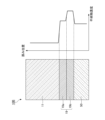
- FIG. 2 is a diagram showing a silicon carbide substrate 10A according to a first example of an embodiment.
- the left figure shows a cross-sectional view of the silicon carbide substrate 10A
- the right figure shows an impurity concentration profile of the silicon carbide substrate 10A.
- the silicon carbide substrate 10A mainly includes a silicon carbide single crystal substrate 50, a recombination promotion layer 19, and a drift region 11.
- Silicon carbide single crystal substrate 50 contains an n-type impurity such as nitrogen and has an n-type.
- the effective concentration of the n-type impurity in silicon carbide single crystal substrate 50 is, for example, not less than 1 ⁇ 10 18 cm ⁇ 3 and not more than 7 ⁇ 10 18 cm ⁇ 3 .
- the recombination promotion layer 19 is provided on a silicon carbide single crystal substrate 50.
- the recombination promotion layer 19 has a first region 19a, a second region 19b, and a third region 19c.
- the first region 19a is provided on the second region 19b.
- the first region 19a is in contact with the drift region 11.
- the first region 19a contains an n-type impurity such as nitrogen or phosphorus, and has an n-type.
- the effective concentration of the n-type impurity in the first region 19a is higher than the effective concentration of the n-type impurity in the silicon carbide single crystal substrate 50.
- the effective concentration of the n-type impurity in the first region 19a is, for example, not less than 5 ⁇ 10 18 cm ⁇ 3 and not more than 2 ⁇ 10 19 cm ⁇ 3 .
- the second region 19b is provided on the third region 19c.
- the second region 19b is provided at a position separated from the upper surface of the recombination promotion layer 19.
- the second region 19b is provided between the first region 19a and the third region 19c.
- the second region 19b contains n-type impurities such as nitrogen or phosphorus and has an n-type.
- the effective concentration of the n-type impurity in the second region 19b is higher than the effective concentration of the n-type impurity in the first region 19a.
- the effective concentration of the n-type impurity in the second region 19b is, for example, 1 ⁇ 10 19 cm ⁇ 3 or more.
- the third region 19c is provided on the silicon carbide single crystal substrate 50.
- the third region 19c is in contact with the silicon carbide single crystal substrate 50.
- the third region 19c contains an n-type impurity such as nitrogen or phosphorus and has an n-type.
- the effective concentration of the n-type impurity in the third region 19c is, for example, the same as the effective concentration of the n-type impurity in the first region 19a. In this case, the third region 19c has a lower concentration than the second region 19b. Therefore, the lattice mismatch with the silicon carbide single crystal substrate 50 is reduced, and thus defect generation can be suppressed.
- the effective concentration of the n-type impurity in the third region 19c is, for example, 5 ⁇ 10 18 cm ⁇ 3 or more and 2 ⁇ 10 19 cm ⁇ 3 or less.
- the drift region 11 is provided on the recombination promotion layer 19.
- the drift region 11 is in contact with the first region 19a.
- the drift region 11 contains n-type impurities such as nitrogen or phosphorus and has an n-type.
- the effective concentration of the n-type impurity in the drift region 11 is, for example, not less than 1 ⁇ 10 14 cm ⁇ 3 and not more than 5 ⁇ 10 16 cm ⁇ 3 .
- the recombination promotion layer 19 has a first region 19a and a second region 19b.
- the first region 19a is provided on the second region 19b.
- the effective concentration of n-type impurities in the second region 19b is higher than the effective concentration of n-type impurities in the first region 19a.
- the impurity concentration in the outermost region (first region 19a) of the recombination promotion layer 19 is low, stacking faults are unlikely to be formed in the outermost surface of the recombination promotion layer 19. Therefore, stacking faults are prevented from being inherited from the recombination promotion layer 19 to the drift region 11.
- second region 19b since a region (second region 19b) with a high impurity concentration exists in the recombination promotion layer 19, the recombination of carriers is promoted. Therefore, the recombination efficiency is improved and the required thickness of the recombination promotion layer 19 can be reduced. Reducing the required thickness of the recombination promotion layer 19 shortens the time required for epitaxial growth when forming the recombination promotion layer 19, thereby reducing manufacturing costs.
- a silicon carbide single crystal substrate 50 is prepared.
- the silicon carbide single crystal substrate 50 contains n-type impurities such as nitrogen and has an n-type.
- the recombination promotion layer 19 is formed on the silicon carbide single crystal substrate 50. Specifically, the recombination promotion layer 19 is formed on the silicon carbide single crystal substrate 50 by epitaxial growth with the addition of n-type impurities such as nitrogen or phosphorus. Next, ions are implanted into the recombination promotion layer 19. A second region 19b is formed at a position separated from the upper surface of the recombination promotion layer 19 by the ion implantation. As the second region 19b is formed, a first region 19a is formed on the second region 19b of the recombination promotion layer 19, and a third region 19c is formed below the second region 19b of the recombination promotion layer 19. In the ion implantation to form the second region 19b, for example, an n-type impurity such as nitrogen or phosphorus is implanted.
- a silicon carbide epitaxial layer 40 is formed on the recombination promotion layer 19.
- the silicon carbide epitaxial layer 40 can be formed by epitaxial growth with the addition of an n-type impurity such as nitrogen.
- ions are implanted into the silicon carbide epitaxial layer 40.
- the body region 12, the source region 13, and the contact region 18 are formed by ion implantation.
- the remaining portion of the silicon carbide epitaxial layer 40 functions as the drift region 11.
- a p-type impurity such as aluminum is ion implanted.
- an n-type impurity such as phosphorus is ion implanted.
- a silicon carbide substrate 10A can be manufactured in which a recombination promotion layer 19 and a silicon carbide epitaxial layer 40 are formed in this order on a silicon carbide single crystal substrate 50.
- the second region 19b is formed at a position separated from the upper surface of the recombination promotion layer 19 by ion implantation into the recombination promotion layer 19.
- the first region 19a is formed on the second region 19b of the recombination promotion layer 19.
- the effective concentration of the n-type impurity in the second region 19b is higher than the effective concentration of the n-type impurity in the first region 19a.
- the impurity concentration in the outermost region (first region 19a) of the recombination promotion layer 19 is low, stacking faults are unlikely to be formed on the outermost surface of the recombination promotion layer 19. Therefore, the transfer of stacking faults from the recombination promotion layer 19 to the drift region 11 is suppressed.
- the recombination of carriers is promoted. This improves recombination efficiency and reduces the required thickness of the recombination promotion layer 19. Reducing the required thickness of the recombination promotion layer 19 shortens the time required for epitaxial growth when forming the recombination promotion layer 19, thereby reducing manufacturing costs.
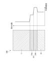
- FIG. 3 is a diagram showing a silicon carbide substrate 10B according to a second example of an embodiment.
- the left figure shows a cross-sectional view of the silicon carbide substrate 10B
- the right figure shows an impurity concentration profile of the silicon carbide substrate 10B.
- Silicon carbide substrate 10B differs from silicon carbide substrate 10A in that recombination promotion layer 19 does not have third region 19c, but has first region 19a and second region 19b.
- the rest of the configuration of silicon carbide substrate 10B is the same as, for example, silicon carbide substrate 10A. The following description will focus on the configuration that differs from silicon carbide substrate 10A.
- the recombination promotion layer 19 has a first region 19a and a second region 19b.
- the first region 19a is provided on the second region 19b.
- the first region 19a contacts the drift region 11.
- the second region 19b is provided on the silicon carbide single crystal substrate 50.
- the second region 19b is provided at a position spaced apart from the upper surface of the recombination promotion layer 19.
- the second region 19b contacts the silicon carbide single crystal substrate 50.
- the recombination promotion layer 19 has a first region 19a and a second region 19b.
- the first region 19a is provided on the second region 19b.
- the effective concentration of n-type impurities in the second region 19b is higher than the effective concentration of n-type impurities in the first region 19a.
- the same effects as those of the silicon carbide substrate 10A and the silicon carbide semiconductor device 100 having the silicon carbide substrate 10A can be obtained.
- Silicon carbide substrate 10B can be manufactured, for example, by a method similar to that for silicon carbide substrate 10A.
- the method for manufacturing silicon carbide substrate 10B provides the same effects as the method for manufacturing silicon carbide substrate 10A.
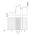
- FIG. 4 is a diagram showing a silicon carbide substrate 10C according to a third example of an embodiment.
- the left figure shows a cross-sectional view of the silicon carbide substrate 10C
- the right figure shows an impurity concentration profile of the silicon carbide substrate 10C.
- the silicon carbide substrate 10C mainly includes a silicon carbide single crystal substrate 50, a buffer layer 20, and a drift region 11.
- the buffer layer 20 is provided on a silicon carbide single crystal substrate 50.
- the buffer layer 20 has a fourth region 20a, a fifth region 20b, and a sixth region 20c.
- the fourth region 20a is provided on the fifth region 20b.
- the fourth region 20a contacts the drift region 11.
- the fourth region 20a contains an n-type impurity such as nitrogen or phosphorus, and has an n-type.
- the effective concentration of the n-type impurity in the fourth region 20a is lower than the effective concentration of the n-type impurity in the silicon carbide single crystal substrate 50.
- the effective concentration of the n-type impurity in the fourth region 20a is, for example, 2 ⁇ 10 17 cm ⁇ 3 or more and 3 ⁇ 10 18 cm ⁇ 3 or less.
- the effective concentration of the n-type impurity in the fourth region 20a is approximately constant, and the effective concentration of the n-type impurity at the interface between the fourth region 20a and the drift region 11 may be abruptly switched from the concentration in the fourth region 20a to the concentration in the drift region 11. In this case, the resistance of the silicon carbide semiconductor device 100 is unlikely to be high. In contrast, when the effective concentration of n-type impurities in fourth region 20a continuously decreases toward drift region 11, the resistance of silicon carbide semiconductor device 100 is likely to increase.
- the fifth region 20b is provided on the sixth region 20c.
- the fifth region 20b is provided at a position separated from the upper surface of the buffer layer 20.
- the fifth region 20b is provided between the fourth region 20a and the sixth region 20c.
- the fifth region 20b contains an n-type impurity such as nitrogen or phosphorus, and has an n-type.
- the effective concentration of the n-type impurity in the fifth region 20b is higher than the effective concentration of the n-type impurity in the silicon carbide single crystal substrate 50.
- the effective concentration of the n-type impurity in the fifth region 20b is, for example, 1 ⁇ 10 19 cm ⁇ 3 or more.
- the sixth region 20c is provided on the silicon carbide single crystal substrate 50.
- the sixth region 20c is in contact with the silicon carbide single crystal substrate 50.
- the sixth region 20c contains n-type impurities such as nitrogen or phosphorus, and has an n-type.
- the effective concentration of the n-type impurities in the sixth region 20c is, for example, the same as the effective concentration of the n-type impurities in the fourth region 20a. In this case, the sixth region 20c has a lower concentration than the fifth region 20b. Therefore, the lattice mismatch with the silicon carbide single crystal substrate 50 is reduced, and thus defect generation can be suppressed.
- the effective concentration of the n-type impurities in the sixth region 20c is, for example, 2 ⁇ 10 17 cm ⁇ 3 or more and 3 ⁇ 10 18 cm ⁇ 3 or less.
- the drift region 11 is provided on the buffer layer 20.
- the drift region 11 is in contact with the fourth region 20a.
- the drift region 11 contains an n-type impurity such as nitrogen or phosphorus and has an n-type.
- the effective concentration of the n-type impurity in the drift region 11 is, for example, not less than 1 ⁇ 10 14 cm ⁇ 3 and not more than 5 ⁇ 10 16 cm ⁇ 3 .
- the buffer layer 20 has a fourth region 20a and a fifth region 20b.
- the fourth region 20a is provided on the fifth region 20b.
- the effective concentration of n-type impurities in the fifth region 20b is higher than the effective concentration of n-type impurities in the fourth region 20a.
- the impurity concentration in the outermost region (fourth region 20a) of the buffer layer 20 is low, stacking faults are unlikely to be formed in the outermost surface of the buffer layer 20. Therefore, stacking faults are prevented from being inherited from the buffer layer 20 to the drift region 11.
- the buffer layer 20 since a region (fifth region 20b) with a high impurity concentration exists in the buffer layer 20, carrier recombination is promoted. Therefore, the recombination efficiency is improved and the required thickness of the buffer layer 20 can be reduced. Reducing the required thickness of the buffer layer 20 shortens the time required for epitaxial growth when forming the buffer layer 20, thereby reducing manufacturing costs.
- a silicon carbide single crystal substrate 50 is prepared.
- the silicon carbide single crystal substrate 50 contains n-type impurities such as nitrogen and has an n-type.
- the buffer layer 20 is formed on the silicon carbide single crystal substrate 50.
- the buffer layer 20 is formed on the silicon carbide single crystal substrate 50 by epitaxial growth with the addition of n-type impurities such as nitrogen or phosphorus.
- ions are implanted into the buffer layer 20.
- a fifth region 20b is formed at a position separated from the upper surface of the buffer layer 20 by the ion implantation. With the formation of the fifth region 20b, a fourth region 20a is formed on the fifth region 20b of the buffer layer 20, and a sixth region 20c is formed below the fifth region 20b of the buffer layer 20.
- an n-type impurity such as nitrogen or phosphorus is implanted.
- a silicon carbide epitaxial layer 40 is formed on the buffer layer 20.
- the method for forming the silicon carbide epitaxial layer 40 may be the same as the method for forming the silicon carbide epitaxial layer 40 in the method for manufacturing the silicon carbide substrate 10A.
- a silicon carbide substrate 10C can be manufactured in which a buffer layer 20 and a silicon carbide epitaxial layer 40 are formed in this order on a silicon carbide single crystal substrate 50.
- the fifth region 20b is formed at a position separated from the upper surface of the buffer layer 20 by ion implantation into the buffer layer 20.
- the fourth region 20a is formed on the fifth region 20b of the buffer layer 20.
- the effective concentration of n-type impurities in the fifth region 20b is higher than the effective concentration of n-type impurities in the fourth region 20a. In this case, since the impurity concentration in the outermost region (fourth region 20a) of the buffer layer 20 is low, stacking faults are unlikely to be formed in the outermost surface of the buffer layer 20.
- FIG. 5 is a diagram showing a silicon carbide substrate 10D according to a fourth embodiment.
- the left figure shows a cross-sectional view of the silicon carbide substrate 10D
- the right figure shows an impurity concentration profile of the silicon carbide substrate 10D.
- Silicon carbide substrate 10D differs from silicon carbide substrate 10C in that buffer layer 20 does not have sixth region 20c, but has fourth region 20a and fifth region 20b.
- Other configurations of silicon carbide substrate 10D are the same as, for example, silicon carbide substrate 10C. The following description will focus on the configurations that differ from silicon carbide substrate 10C.
- the buffer layer 20 has a fourth region 20a and a fifth region 20b.
- the fourth region 20a is provided on the fifth region 20b.
- the fourth region 20a contacts the drift region 11.
- the fifth region 20b is provided on the silicon carbide single crystal substrate 50.
- the fifth region 20b is provided at a position spaced apart from the upper surface of the recombination promotion layer 19.
- the fifth region 20b contacts the silicon carbide single crystal substrate 50.
- the buffer layer 20 has a fourth region 20a and a fifth region 20b.
- the fourth region 20a is provided on the fifth region 20b.
- the effective concentration of n-type impurities in the fifth region 20b is higher than the effective concentration of n-type impurities in the fourth region 20a. In this case, the same effects as those of the silicon carbide substrate 10C and the silicon carbide semiconductor device 100 having the silicon carbide substrate 10C can be obtained.
- Silicon carbide substrate 10D can be manufactured, for example, by a method similar to that for silicon carbide substrate 10C.
- the method for manufacturing silicon carbide substrate 10D provides the same effects as the method for manufacturing silicon carbide substrate 10C.
- FIG. 6 is a diagram showing a silicon carbide substrate 10E according to a fifth embodiment.
- the left figure shows a cross-sectional view of the silicon carbide substrate 10E
- the right figure shows an impurity concentration profile of the silicon carbide substrate 10E.
- Silicon carbide substrate 10E differs from silicon carbide substrate 10A in that it has a buffer layer 21 between silicon carbide single crystal substrate 50 and recombination promotion layer 19.
- the rest of the configuration of silicon carbide substrate 10E is the same as, for example, silicon carbide substrate 10A. Below, the configuration that differs from silicon carbide substrate 10A will be mainly described.
- the silicon carbide substrate 10E mainly includes a silicon carbide single crystal substrate 50, a buffer layer 21, a recombination promotion layer 19, and a drift region 11.
- the buffer layer 21 is provided on the silicon carbide single crystal substrate 50.
- the buffer layer 21 is provided between the silicon carbide single crystal substrate 50 and the recombination promotion layer 19.
- the buffer layer 21 contains an n-type impurity such as nitrogen or phosphorus, and has an n-type.
- the effective concentration of the n-type impurity in the buffer layer 21 is lower than the effective concentration of the n-type impurity in the silicon carbide single crystal substrate 50.
- the effective concentration of the n-type impurity in the buffer layer 21 is, for example, not less than 2 ⁇ 10 17 cm ⁇ 3 and not more than 3 ⁇ 10 18 cm ⁇ 3 .
- the recombination promotion layer 19 has a first region 19a and a second region 19b.
- the first region 19a is provided on the second region 19b.
- the effective concentration of n-type impurities in the second region 19b is higher than the effective concentration of n-type impurities in the first region 19a.
- the same effects as those of the silicon carbide substrate 10A and the silicon carbide semiconductor device 100 having the silicon carbide substrate 10A can be obtained.
- the buffer layer 21 is provided between the silicon carbide single crystal substrate 50 and the recombination promotion layer 19.
- the basal plane dislocations present in the silicon carbide single crystal substrate 50 are easily converted to threading edge dislocations at the interface between the silicon carbide single crystal substrate 50 and the buffer layer 21. Therefore, the basal plane dislocations can be prevented from reaching the drift region 11.
- the expansion of stacking faults in the drift region 11 is prevented when a current is applied in the forward direction to the pn junction, and as a result, the increase in the on-voltage can be prevented.
- a silicon carbide single crystal substrate 50 is prepared.
- the silicon carbide single crystal substrate 50 contains n-type impurities such as nitrogen and has an n-type.
- a buffer layer 21 is formed on the silicon carbide single crystal substrate 50.
- the buffer layer 21 is formed on the silicon carbide single crystal substrate 50 by epitaxial growth with the addition of n-type impurities such as nitrogen or phosphorus.
- the recombination promotion layer 19 is formed on the buffer layer 21.
- the method for forming the recombination promotion layer 19 may be the same as the method for forming the recombination promotion layer 19 in the manufacturing method of the silicon carbide substrate 10A.
- a silicon carbide epitaxial layer 40 is formed on the recombination promotion layer 19.
- the method for forming the silicon carbide epitaxial layer 40 may be the same as the method for forming the silicon carbide epitaxial layer 40 in the method for manufacturing the silicon carbide substrate 10A.
- a silicon carbide substrate 10E can be manufactured in which a buffer layer 21 and a silicon carbide epitaxial layer 40 are formed in this order on a silicon carbide single crystal substrate 50.
- the second region 19b is formed at a position separated from the upper surface of the recombination promotion layer 19 by ion implantation into the recombination promotion layer 19.
- the first region 19a is formed on the second region 19b of the recombination promotion layer 19.
- the effective concentration of the n-type impurity in the second region 19b is higher than the effective concentration of the n-type impurity in the first region 19a. In this case, the same effects as those of the silicon carbide substrate 10A and the silicon carbide semiconductor device 100 having the silicon carbide substrate 10A can be obtained.
- buffer layer 21 is grown by epitaxial growth on silicon carbide single crystal substrate 50
- basal plane dislocations present in silicon carbide single crystal substrate 50 are likely to be converted to threading edge dislocations at the interface between silicon carbide single crystal substrate 50 and buffer layer 21. Therefore, basal plane dislocations can be prevented from reaching drift region 11.
- the expansion of stacking faults in drift region 11 when forward current is applied to the pn junction is prevented, and as a result, an increase in on-voltage can be prevented.
- FIG. 7 is a diagram showing a silicon carbide substrate 10F according to a sixth embodiment.
- the left diagram shows a cross-sectional view of the silicon carbide substrate 10F
- the right diagram shows an impurity concentration profile of the silicon carbide substrate 10F.
- Silicon carbide substrate 10F differs from silicon carbide substrate 10E in that recombination promotion layer 19 does not have third region 19c, but has first region 19a and second region 19b.
- the rest of the configuration of silicon carbide substrate 10F is the same as, for example, silicon carbide substrate 10E. The following description will focus on the configuration that differs from silicon carbide substrate 10E.
- the recombination promotion layer 19 has a first region 19a and a second region 19b.
- the first region 19a is provided on the second region 19b.
- the first region 19a contacts the drift region 11.
- the second region 19b is provided on the silicon carbide single crystal substrate 50.
- the second region 19b is provided at a position spaced apart from the upper surface of the recombination promotion layer 19.
- the second region 19b contacts the silicon carbide single crystal substrate 50.
- the recombination promotion layer 19 has a first region 19a and a second region 19b.
- the first region 19a is provided on the second region 19b.
- the effective concentration of n-type impurities in the second region 19b is higher than the effective concentration of n-type impurities in the first region 19a.
- the same effects as those of the silicon carbide substrate 10E and the silicon carbide semiconductor device 100 having the silicon carbide substrate 10E can be obtained.
- Silicon carbide substrate 10F can be manufactured, for example, by a method similar to that for silicon carbide substrate 10E.
- the manufacturing method for silicon carbide substrate 10F provides the same effects as the manufacturing method for silicon carbide substrate 10E.
- the effective concentration of p-type impurities and the effective concentration of n-type impurities in each of the above impurity regions can be measured using a scanning capacitance microscope (SCM) method or a secondary ion mass spectrometry (SIMS) method, for example.
- SCM scanning capacitance microscope
- SIMS secondary ion mass spectrometry
- Silicon carbide substrate 10A Silicon carbide substrate 10B Silicon carbide substrate 10C Silicon carbide substrate 10D Silicon carbide substrate 10E Silicon carbide substrate 10F Silicon carbide substrate 11 Drift region 12 Body region 13 Source region 18 Contact region 19 Recombination promotion layer 19a First region 19b Second region 19c Third region 20 Buffer layer 20a Fourth region 20b Fifth region 20c Sixth region 21 Buffer layer 40 Silicon carbide epitaxial layer 50 Silicon carbide single crystal substrate 60 Source electrode 61 Contact electrode 62 Source wiring 70 Drain electrode 81 Gate insulating film 82 Gate electrode 83 Interlayer insulating film 90 Contact hole 100 Silicon carbide semiconductor device
Landscapes
- Recrystallisation Techniques (AREA)
- Crystals, And After-Treatments Of Crystals (AREA)
Abstract
Description
炭化珪素エピタキシャル層を薄くする場合、炭化珪素エピタキシャル層の不純物濃度を高くすることが有効である。しかしながら、炭化珪素エピタキシャル層の不純物濃度を高くすると、結晶歪みにより炭化珪素エピタキシャル層に積層欠陥が形成されやすい。積層欠陥が形成されると、炭化珪素エピタキシャル層の上に形成されるドリフト層にも積層欠陥が拡張する。
本開示によれば、再結合効率を向上し、必要な炭化珪素エピタキシャル層の厚みを低減できる炭化珪素基板、炭化珪素半導体装置および炭化珪素半導体装置の製造方法を提供できる。
最初に本開示の実施態様を列記して説明する。以下の説明では、同一または対応する要素には同一の符号を付し、それらについて同じ説明は繰り返さない。
以下、本開示の実施形態について詳細に説明するが、本開示はこれらに限定されるものではない。
実施形態に係る炭化珪素半導体装置100について説明する。図1は、実施形態に係る炭化珪素半導体装置100を示す断面図である。
次に、実施形態に係る炭化珪素半導体装置100が有する炭化珪素基板10について説明する。
2 第2主面
3 側面
4 底面
5 ゲートトレンチ
10 炭化珪素基板
10A 炭化珪素基板
10B 炭化珪素基板
10C 炭化珪素基板
10D 炭化珪素基板
10E 炭化珪素基板
10F 炭化珪素基板
11 ドリフト領域
12 ボディ領域
13 ソース領域
18 コンタクト領域
19 再結合促進層
19a 第1領域
19b 第2領域
19c 第3領域
20 バッファ層
20a 第4領域
20b 第5領域
20c 第6領域
21 バッファ層
40 炭化珪素エピタキシャル層
50 炭化珪素単結晶基板
60 ソース電極
61 コンタクト電極
62 ソース配線
70 ドレイン電極
81 ゲート絶縁膜
82 ゲート電極
83 層間絶縁膜
90 コンタクトホール
100 炭化珪素半導体装置
Claims (9)
- 第1導電型を有する炭化珪素単結晶基板と、
前記炭化珪素単結晶基板の上に設けられ、前記第1導電型を有する炭化珪素エピタキシャル層と、
前記炭化珪素エピタキシャル層の上に設けられ、前記第1導電型を有するドリフト層と、
を有し、
前記炭化珪素エピタキシャル層は、第1領域と、第2領域とを有し、
前記第1領域は、前記第2領域の上に位置し、
前記第1領域の不純物濃度は、前記炭化珪素単結晶基板の不純物濃度よりも高く、
前記第2領域の不純物濃度は、前記第1領域の不純物濃度よりも高い、
炭化珪素基板。 - 前記炭化珪素エピタキシャル層は、前記炭化珪素単結晶基板と前記第2領域との間に設けられる第3領域を有し、
前記第3領域の不純物濃度は、前記第1領域の不純物濃度と同じである、
請求項1に記載の炭化珪素基板。 - 前記炭化珪素単結晶基板と前記炭化珪素エピタキシャル層との間に設けられ、前記第1導電型を有するバッファ層を有し、
前記バッファ層の不純物濃度は、前記炭化珪素単結晶基板の不純物濃度よりも低い、
請求項1または請求項2に記載の炭化珪素基板。 - 第1導電型を有する炭化珪素単結晶基板と、
前記炭化珪素単結晶基板の上に設けられ、前記第1導電型を有するバッファ層と、
前記バッファ層の上に設けられ、前記第1導電型を有するドリフト層と、
を有し、
前記バッファ層は、第4領域と、第5領域とを有し、
前記第4領域は、前記第5領域の上に位置し、
前記第4領域の不純物濃度は、前記炭化珪素単結晶基板の不純物濃度よりも低く、
前記第5領域の不純物濃度は、前記炭化珪素単結晶基板の不純物濃度よりも高い、
炭化珪素基板。 - 前記バッファ層は、前記炭化珪素単結晶基板と前記第5領域との間に設けられる第6領域を有し、
前記第6領域の不純物濃度は、前記第4領域の不純物濃度と同じである、
請求項4に記載の炭化珪素基板。 - 第1主面と、前記第1主面と反対の第2主面とを有する炭化珪素基板を備え、
前記炭化珪素基板は、
第1導電型を有する炭化珪素単結晶基板と、
前記炭化珪素単結晶基板の上に設けられ、前記第1導電型を有する炭化珪素エピタキシャル層と、
前記炭化珪素エピタキシャル層の上に設けられ、前記第1導電型を有するドリフト層と、
を有し、
前記炭化珪素エピタキシャル層は、第1領域と、第2領域とを有し、
前記第1領域は、前記第2領域の上に位置し、
前記第1領域の不純物濃度は、前記炭化珪素単結晶基板の不純物濃度よりも高く、
前記第2領域の不純物濃度は、前記第1領域の不純物濃度よりも高い、
炭化珪素半導体装置。 - 第1主面と、前記第1主面と反対の第2主面とを有する炭化珪素基板を備え、
前記炭化珪素基板は、
第1導電型を有する炭化珪素単結晶基板と、
前記炭化珪素単結晶基板の上に設けられ、前記第1導電型を有するバッファ層と、
前記バッファ層の上に設けられ、前記第1導電型を有するドリフト層と、
を有し、
前記バッファ層は、第4領域と、第5領域とを有し、
前記第4領域は、前記第5領域の上に位置し、
前記第4領域の不純物濃度は、前記炭化珪素単結晶基板の不純物濃度よりも低く、
前記第5領域の不純物濃度は、前記炭化珪素単結晶基板の不純物濃度よりも高い、
炭化珪素半導体装置。 - 第1導電型を有する炭化珪素単結晶基板の上に、前記第1導電型を有し、前記炭化珪素単結晶基板よりも不純物濃度が高い炭化珪素エピタキシャル層を形成する工程と、
前記炭化珪素エピタキシャル層へのイオン注入により、前記炭化珪素エピタキシャル層の上面から離隔した位置に前記第1導電型を有する第2領域を形成する工程と、
前記第2領域を形成する工程の後、前記炭化珪素エピタキシャル層の上に、前記第1導電型を有するドリフト層を形成する工程と、
を有し、
前記第2領域の形成に伴って、前記炭化珪素エピタキシャル層の前記第2領域の上に第1領域が形成され、
前記第1領域の不純物濃度は、前記炭化珪素単結晶基板の不純物濃度よりも高く、
前記第2領域の不純物濃度は、前記第1領域の不純物濃度よりも高い、
炭化珪素基板の製造方法。 - 第1導電型を有する炭化珪素単結晶基板の上に、前記第1導電型を有し、前記炭化珪素単結晶基板よりも不純物濃度が低いバッファ層を形成する工程と、
前記バッファ層へのイオン注入により、前記バッファ層の上面から離隔した位置に前記第1導電型を有する第5領域を形成する工程と、
前記第5領域を形成する工程の後、前記バッファ層の上に、前記第1導電型を有するドリフト層を形成する工程と、
を有し、
前記第5領域の形成に伴って、前記バッファ層の前記第5領域の上に第4領域が形成され、
前記第4領域の不純物濃度は、前記炭化珪素単結晶基板の不純物濃度よりも低く、
前記第5領域の不純物濃度は、前記炭化珪素単結晶基板の不純物濃度よりも高い、
炭化珪素基板の製造方法。
Priority Applications (3)
| Application Number | Priority Date | Filing Date | Title |
|---|---|---|---|
| JP2025525972A JPWO2024252795A1 (ja) | 2023-06-08 | 2024-04-16 | |
| DE112024002456.4T DE112024002456T5 (de) | 2023-06-08 | 2024-04-16 | Siliziumkarbidsubstrat, Siliziumkarbid-Halbleiterelement und Verfahren zur Herstellung eines Siliziumkarbidsubstrats |
| CN202480025712.0A CN121014273A (zh) | 2023-06-08 | 2024-04-16 | 碳化硅衬底、碳化硅半导体装置及碳化硅衬底的制造方法 |
Applications Claiming Priority (2)
| Application Number | Priority Date | Filing Date | Title |
|---|---|---|---|
| JP2023-094793 | 2023-06-08 | ||
| JP2023094793 | 2023-06-08 |
Publications (1)
| Publication Number | Publication Date |
|---|---|
| WO2024252795A1 true WO2024252795A1 (ja) | 2024-12-12 |
Family
ID=93795382
Family Applications (1)
| Application Number | Title | Priority Date | Filing Date |
|---|---|---|---|
| PCT/JP2024/015148 Ceased WO2024252795A1 (ja) | 2023-06-08 | 2024-04-16 | 炭化珪素基板、炭化珪素半導体装置および炭化珪素基板の製造方法 |
Country Status (4)
| Country | Link |
|---|---|
| JP (1) | JPWO2024252795A1 (ja) |
| CN (1) | CN121014273A (ja) |
| DE (1) | DE112024002456T5 (ja) |
| WO (1) | WO2024252795A1 (ja) |
Citations (4)
| Publication number | Priority date | Publication date | Assignee | Title |
|---|---|---|---|---|
| WO2017094764A1 (ja) * | 2015-12-02 | 2017-06-08 | 三菱電機株式会社 | 炭化珪素エピタキシャル基板および炭化珪素半導体装置 |
| WO2018150861A1 (ja) * | 2017-02-20 | 2018-08-23 | 日立金属株式会社 | 炭化ケイ素積層基板およびその製造方法 |
| WO2018207394A1 (ja) * | 2017-05-10 | 2018-11-15 | 三菱電機株式会社 | 半導体装置及びその製造方法 |
| JP2020141109A (ja) * | 2019-03-01 | 2020-09-03 | 三菱電機株式会社 | SiCエピタキシャルウエハ、半導体装置、電力変換装置 |
Family Cites Families (1)
| Publication number | Priority date | Publication date | Assignee | Title |
|---|---|---|---|---|
| JP2023094793A (ja) | 2021-12-24 | 2023-07-06 | 帝人ファーマ株式会社 | 睡眠時無呼吸症候群の診断を補助する方法、睡眠時無呼吸症候群の診断を補助するための装置、及び睡眠時無呼吸症候群の診断を補助するためのキット |
-
2024
- 2024-04-16 DE DE112024002456.4T patent/DE112024002456T5/de active Pending
- 2024-04-16 CN CN202480025712.0A patent/CN121014273A/zh active Pending
- 2024-04-16 JP JP2025525972A patent/JPWO2024252795A1/ja active Pending
- 2024-04-16 WO PCT/JP2024/015148 patent/WO2024252795A1/ja not_active Ceased
Patent Citations (4)
| Publication number | Priority date | Publication date | Assignee | Title |
|---|---|---|---|---|
| WO2017094764A1 (ja) * | 2015-12-02 | 2017-06-08 | 三菱電機株式会社 | 炭化珪素エピタキシャル基板および炭化珪素半導体装置 |
| WO2018150861A1 (ja) * | 2017-02-20 | 2018-08-23 | 日立金属株式会社 | 炭化ケイ素積層基板およびその製造方法 |
| WO2018207394A1 (ja) * | 2017-05-10 | 2018-11-15 | 三菱電機株式会社 | 半導体装置及びその製造方法 |
| JP2020141109A (ja) * | 2019-03-01 | 2020-09-03 | 三菱電機株式会社 | SiCエピタキシャルウエハ、半導体装置、電力変換装置 |
Also Published As
| Publication number | Publication date |
|---|---|
| DE112024002456T5 (de) | 2026-03-26 |
| CN121014273A (zh) | 2025-11-25 |
| JPWO2024252795A1 (ja) | 2024-12-12 |
Similar Documents
| Publication | Publication Date | Title |
|---|---|---|
| US11978778B2 (en) | Semiconductor device | |
| CN102714143B (zh) | 外延片以及半导体元件 | |
| JP5431667B2 (ja) | 窒化ガリウム半導体装置 | |
| US7531889B2 (en) | Epitaxial substrate and semiconductor element | |
| JP7574892B2 (ja) | 炭化珪素半導体装置の製造方法 | |
| JP2019140186A (ja) | 半導体装置、基板、半導体装置の製造方法、及び、基板の製造方法。 | |
| US11177380B2 (en) | Silicon carbide semiconductor component | |
| JP2011140429A (ja) | エピタキシャルウエハ及び半導体素子 | |
| WO2024252795A1 (ja) | 炭化珪素基板、炭化珪素半導体装置および炭化珪素基板の製造方法 | |
| JP2009054659A (ja) | 窒化ガリウム半導体装置の製造方法 | |
| JP2019140187A (ja) | 半導体装置、基板、半導体装置の製造方法、及び、基板の製造方法。 | |
| US20220181504A1 (en) | Semiconductor device and production method for semiconductor device | |
| CN114678424A (zh) | 具有改进特性的碳化硅mosfet晶体管器件及对应的制造方法 | |
| JP2021005736A (ja) | 半導体装置、基板、半導体装置の製造方法、及び、基板の製造方法 | |
| JP7601240B2 (ja) | 炭化珪素半導体装置および炭化珪素半導体基板 | |
| KR20190127324A (ko) | 반도체 소자 및 그 제조 방법 | |
| KR20120029703A (ko) | 질화물계 반도체 소자 및 그 제조 방법 |
Legal Events
| Date | Code | Title | Description |
|---|---|---|---|
| 121 | Ep: the epo has been informed by wipo that ep was designated in this application |
Ref document number: 24819033 Country of ref document: EP Kind code of ref document: A1 |
|
| ENP | Entry into the national phase |
Ref document number: 2025525972 Country of ref document: JP Kind code of ref document: A |
|
| WWE | Wipo information: entry into national phase |
Ref document number: 2025525972 Country of ref document: JP |
|
| WWE | Wipo information: entry into national phase |
Ref document number: 112024002456 Country of ref document: DE |
|
| WWP | Wipo information: published in national office |
Ref document number: 112024002456 Country of ref document: DE |