WO2024252848A1 - Solid-state imaging element and method for controlling solid-state imaging element - Google Patents
Solid-state imaging element and method for controlling solid-state imaging element Download PDFInfo
- Publication number
- WO2024252848A1 WO2024252848A1 PCT/JP2024/017442 JP2024017442W WO2024252848A1 WO 2024252848 A1 WO2024252848 A1 WO 2024252848A1 JP 2024017442 W JP2024017442 W JP 2024017442W WO 2024252848 A1 WO2024252848 A1 WO 2024252848A1
- Authority
- WO
- WIPO (PCT)
- Prior art keywords
- solid
- bias voltage
- state imaging
- illuminance
- pixel
- Prior art date
- Legal status (The legal status is an assumption and is not a legal conclusion. Google has not performed a legal analysis and makes no representation as to the accuracy of the status listed.)
- Ceased
Links
Images












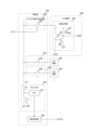


Classifications
-
- H—ELECTRICITY
- H04—ELECTRIC COMMUNICATION TECHNIQUE
- H04N—PICTORIAL COMMUNICATION, e.g. TELEVISION
- H04N25/00—Circuitry of solid-state image sensors [SSIS]; Control thereof
- H04N25/47—Image sensors with pixel address output; Event-driven image sensors; Selection of pixels to be read out based on image data
-
- H—ELECTRICITY
- H04—ELECTRIC COMMUNICATION TECHNIQUE
- H04N—PICTORIAL COMMUNICATION, e.g. TELEVISION
- H04N25/00—Circuitry of solid-state image sensors [SSIS]; Control thereof
- H04N25/70—SSIS architectures; Circuits associated therewith
- H04N25/76—Addressed sensors, e.g. MOS or CMOS sensors
- H04N25/77—Pixel circuitry, e.g. memories, A/D converters, pixel amplifiers, shared circuits or shared components
Definitions
- This technology relates to solid-state imaging devices. More specifically, it relates to solid-state imaging devices that detect changes in luminance, and to a method of controlling the same.
- synchronous solid-state imaging elements that capture image data in synchronization with a synchronization signal such as a vertical synchronization signal have been used in imaging devices.
- This general synchronous solid-state imaging element can only capture image data at every synchronization signal period (e.g., 1/60 seconds). This makes it difficult to respond to requests for faster processing in fields such as transportation and robots. Therefore, an asynchronous solid-state imaging element has been proposed that detects address events in real time for each pixel address based on whether or not the amount of change in luminance of that pixel exceeds a predetermined threshold (see, for example, Non-Patent Document 1).
- a solid-state imaging element that detects address events for each pixel in this way is called an EVS (Event-based Vision Sensor) or a DVS (Dynamic Vision Sensor).
- EVS Event-based Vision Sensor
- DVS Dynamic Vision Sensor
- a buffer and a differentiator are used to determine the amount of change in luminance, and a comparator is used to compare the amount of change with a threshold.
- address events are detected by using a buffer, a differentiator, and a comparator.
- noise may occur within the circuit in a dark state. Although the noise may be reduced by controlling the bias current and capacitance value within the circuit, this may result in an increase in the delay time. As such, it is difficult to suppress noise with the above-mentioned EVS.
- This technology was developed in light of these circumstances, and aims to suppress noise in solid-state imaging elements that detect address events.
- This technology has been made to solve the above-mentioned problems, and its first aspect is a solid-state imaging device that includes an illuminometer that measures illuminance, a detection pixel that detects whether the amount of change in luminance has exceeded a predetermined threshold, and a parameter control circuit that controls the parameters of the detection pixel according to the measured illuminance. This has the effect of suppressing noise.
- the detection pixel may include a photoelectric conversion element that generates a photocurrent, a logarithmic response unit that converts the photocurrent into a logarithmic voltage, a buffer that outputs an output signal corresponding to the logarithmic voltage, a differentiator that differentiates the output signal and supplies a differentiated signal, and a comparator that compares the differentiated signal with a predetermined threshold. This provides the effect of detecting an address event.
- a bias voltage generation circuit may be further provided that generates a bias voltage according to the control of the parameter control circuit and supplies the bias voltage to the detection pixel, and the parameter may include the bias voltage. This provides the effect of suppressing noise by controlling the bias voltage.
- the bias voltage may include a first bias voltage
- the bias voltage generation circuit may supply the first bias voltage to the buffer. This provides the effect of suppressing noise by controlling the bias voltage to the buffer.
- the bias voltage may include a second bias voltage
- the bias voltage generation circuit may supply the second bias voltage to the differentiator. This provides the effect of suppressing noise by controlling the bias voltage to the differentiator.
- the bias voltage may include a third bias voltage
- the bias voltage generation circuit may supply the third bias voltage indicating the threshold value to the comparator. This provides the effect of suppressing noise by controlling the bias voltage to the comparator.
- the detection pixel may include a variable capacitance
- the parameter may include a capacitance value of the variable capacitance. This provides the effect of suppressing noise by controlling the capacitance value.
- variable capacitance may be inserted between the input node and the output node of the logarithmic response unit. This provides the effect of suppressing noise by controlling the capacitance value.
- variable capacitance may be inserted between the output node of the logarithmic response unit and a predetermined reference voltage. This provides the effect of suppressing noise by controlling the capacitance value.
- the parameter control circuit may control the parameters to different values when the illuminance is within a predetermined range and when the illuminance is outside the predetermined range. This has the effect of suppressing noise peaks.
- the detection pixels may be arranged in a pixel array section, and the illuminometer may be disposed outside the pixel array section. This provides the effect of only having the detection pixels arranged in the pixel array section.
- the illuminance meter may include an analog signal generation circuit that generates an analog signal corresponding to the luminance, an analog-to-digital converter that converts the analog signal into a digital signal, and an illuminance calculation unit that calculates the illuminance from the digital signal, and the analog signal generation circuit and the detection pixels may be arranged in a pixel array unit. This provides the effect of improving the accuracy of illuminance measurement.
- the detection pixel may include a first photoelectric conversion element
- the analog signal generation circuit may include a transfer transistor that transfers charge from the second photoelectric conversion element to a floating diffusion layer, a reset transistor that initializes the floating diffusion layer, an amplification transistor that amplifies the voltage of the floating diffusion layer to generate the analog signal, and a selection transistor that supplies the analog signal to the analog-to-digital converter in accordance with a selection signal. This provides the effect of generating a gradation signal.
- the detection pixel may include a photoelectric conversion element
- the analog signal generation circuit may include a transfer transistor that transfers charge from the photoelectric conversion element to a floating diffusion layer, a reset transistor that initializes the floating diffusion layer, an amplification transistor that amplifies the voltage of the floating diffusion layer to generate the analog signal, and a selection transistor that supplies the analog signal to the analog-digital converter in accordance with a selection signal.
- the detection pixel may include a photoelectric conversion element that generates a photocurrent and a logarithmic response unit that converts the photocurrent into a logarithmic voltage
- the analog signal generation circuit may include a changeover switch that connects a power supply node of the logarithmic response unit and the analog-to-digital converter. This provides the effect of reducing the circuit size of the analog signal generation circuit.
- the second aspect of this technology is a solid-state imaging device that includes a measurement unit that measures the value of an electrical signal and outputs a measurement value, a detection pixel that detects whether or not the amount of change in luminance has exceeded a predetermined threshold, and a parameter control circuit that controls the parameters of the detection pixel in response to the measurement value. This provides the effect of suppressing noise.
- the measured value may be a value of a current flowing through the detection pixel. This provides the effect of controlling the parameter according to the current value.
- the measured value may be a voltage value of a predetermined node in the detection pixel. This provides the effect of controlling the parameter according to the voltage value.
- the third aspect of the present technology is a solid-state imaging device that includes an illuminometer that measures illuminance, a first pixel having a first capacitance, a second pixel having a second capacitance, and a readout area selection unit that reads out one of the first and second pixels depending on the illuminance. This provides the effect of suppressing noise.
- 1 is a block diagram showing a configuration example of an imaging device according to a first embodiment of the present technology
- 1 is a block diagram showing a configuration example of a solid-state imaging element according to a first embodiment of the present technology
- 1 is a block diagram showing a configuration example of an EVS pixel according to a first embodiment of the present technology
- 1 is a circuit diagram showing a configuration example of an EVS pixel according to a first embodiment of the present technology.
- 1 is a block diagram showing a configuration example of an EVS pixel having a stacked structure according to a first embodiment of the present technology
- 11 is a graph showing an example of a frequency characteristic when a bias voltage is higher than a predetermined value in the first embodiment of the present technology.
- FIG. 11A to 11C are diagrams illustrating an example of a bias current, noise, and delay according to illuminance in a first modified example of the first embodiment of the present technology
- 11 is a circuit diagram showing a configuration example of an EVS pixel according to a second modified example of the first embodiment of the present technology.
- FIG. 13 is a block diagram showing a configuration example of a solid-state imaging element according to a second embodiment of the present technology
- FIG. 13 is a circuit diagram showing a configuration example of a logarithmic response unit according to a second embodiment of the present technology.
- FIG. 13 is a circuit diagram showing a configuration example of a logarithmic response unit to which a diode-connected nMOS transistor is added according to a second embodiment of the present technology.
- FIG. 13 is a circuit diagram showing a configuration example of a logarithmic response unit to which a coupling capacitance and a switch are added according to a second embodiment of the present technology.
- FIG. 13 is a circuit diagram showing a configuration example of a logarithmic response unit in which an insertion position of a coupling capacitance is changed according to a second embodiment of the present technology.
- FIG. 13 is a diagram illustrating an example of the number of capacitances, noise, and delay according to illuminance in the second embodiment of the present technology.
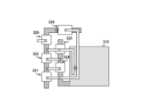
- 13 is a plan view showing an example of a layout of elements in an EVS pixel according to a second embodiment of the present technology.
- FIG. 13 is a plan view showing an example of a layout of elements in an EVS pixel to which a MOS capacitance is added as a coupling capacitance according to a second embodiment of the present technology.
- FIG. 13 is an example of a circuit diagram of an EVS pixel in a case where a logarithmic response unit is switched according to a second embodiment of the present technology.
- 13 is an example of a circuit diagram of an EVS pixel in a case where a sub-pixel is switched according to a second embodiment of the present technology.
- 13 is a block diagram showing a configuration example of a solid-state imaging element according to a first modified example of a second embodiment of the present technology; FIG.
- FIG. 13 is an example of a circuit diagram of an EVS pixel according to a first modified example of the second embodiment of the present technology.
- 13 is an example of a circuit diagram of an EVS pixel according to a second modified example of the second embodiment of the present technology.
- 13 is an example of a circuit diagram of an EVS pixel according to a third modified example of the second embodiment of the present technology.
- FIG. 13 is a block diagram showing a configuration example of a solid-state imaging element according to a third embodiment of the present technology.
- FIG. 13 is a plan view showing an example of a pixel array unit according to a third embodiment of the present technology.
- FIG. 13 is a block diagram showing a configuration example of a solid-state imaging element according to a first modified example of a third embodiment of the present technology.
- FIG. FIG. 13 is a circuit diagram showing a configuration example of a shared block in a first modified example of the third embodiment of the present technology.
- 13 is a block diagram showing a configuration example of a solid-state imaging element according to a second modified example of the third embodiment of the present technology.
- FIG. FIG. 13 is a circuit diagram showing a configuration example of an illuminance meter according to a second modified example of the third embodiment of the present technology.
- 1 is a block diagram showing a schematic configuration example of a vehicle control system;
- FIG. 4 is an explanatory diagram showing an example of an installation position of an imaging unit.
- First embodiment (example of controlling bias voltage according to illuminance) 2.
- Second embodiment (example of controlling capacitance value according to illuminance) 3.
- Third embodiment (an example in which the bias voltage is controlled according to the illuminance and a part of the illuminometer is arranged within the pixel array unit) 4. Examples of applications to moving objects
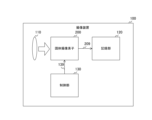
- First embodiment [Configuration example of imaging device] 1 is a block diagram showing an example of a configuration of an imaging device 100 according to a first embodiment of the present technology.
- the imaging device 100 includes an imaging lens 110, a solid-state imaging element 200, a recording unit 120, and a control unit 130.
- Assumed imaging device 100 is a camera mounted on a smartphone, an industrial robot, an in-vehicle camera, or the like.
- the imaging lens 110 focuses the incident light and guides it to the solid-state imaging element 200.
- the solid-state imaging element 200 detects, as an address event, when the amount of change in luminance for each pixel address exceeds a predetermined threshold.
- the solid-state imaging element 200 outputs data indicating the detection result for each pixel to the recording unit 120 via a signal line 209.
- the recording unit 120 records data from the solid-state imaging element 200.
- the control unit 130 controls the solid-state imaging element 200 to detect address events.
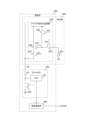
- FIG. 2 is a block diagram showing a configuration example of a solid-state imaging element 200 according to the first embodiment of the present technology.
- the solid-state imaging element 200 includes a readout region selection unit 211, a signal generation unit 212, a pixel array unit 213, a light meter 214, a parameter control circuit 215, and a bias voltage generation circuit 216.
- a pixel array unit 213, a plurality of EVS pixels 300 are arranged in a two-dimensional lattice pattern.
- the EVS pixel 300 detects whether or not the amount of change in luminance exceeds a predetermined threshold (in other words, whether or not an address event has occurred).
- the EVS pixel 300 supplies a detection signal indicating the detection result of the address event to the signal generating unit 212.
- the EVS pixel 300 is an example of a detection pixel as described in the claims.
- the readout region selection unit 211 selects a portion of the multiple EVS pixels 300 included in the pixel array unit 213. For example, the readout region selection unit 211 selects one or more rows among the rows included in the two-dimensional matrix structure corresponding to the pixel array unit 213. The readout region selection unit 211 sequentially selects one or more rows according to a preset period.
- the signal generating unit 212 generates an event signal corresponding to the pixel in which an address event has been detected among the selected pixels based on the output signal of the pixel selected by the readout area selecting unit 211.
- the signal generating unit 212 can be configured to include, for example, a column selection circuit that arbitrates the signals coming into the signal generating unit 212. Furthermore, the signal generating unit 212 can be configured to output not only information about active pixels that detect an address event, but also information about inactive pixels that do not detect an address event.
- the signal generating unit 212 outputs, via the signal line 209, address information and timestamp information (e.g., (X, Y, T)) of the active pixel in which the address event was detected.
- address information and timestamp information e.g., (X, Y, T)
- the data output from the signal generating unit 212 may be not only address information and timestamp information, but also information in a frame format (e.g., (0, 0, 1, 0, ...)).
- the illuminometer 214 measures the illuminance of ambient light. This illuminometer 214 is disposed outside the pixel array section 213.
- the illuminometer 214 is realized by, for example, a photoelectric conversion element, a transistor, or an ADC (Analog to Digital Converter).
- the illuminometer 214 supplies the measured illuminance to the parameter control circuit 215.
- the parameter control circuit 215 controls the parameters of the EVS pixel 300 according to the illuminance measured by the illuminometer 214. For example, the bias voltage among various parameters is controlled.
- the bias voltage generation circuit 216 generates a bias voltage according to the control of the parameter control circuit 215 and supplies it to each of the EVS pixels 300 in the pixel array section 213. Although one bias voltage generation circuit 216 is provided for all pixels, it is also possible to divide the pixel array section 213 into multiple regions and provide a bias voltage generation circuit 216 for each region.
- FIG. 3 is a block diagram showing a configuration example of an EVS pixel according to the first embodiment of the present technology.
- the EVS pixel 300 includes a photoelectric conversion element 310, a logarithmic response unit 320, a buffer 330, a differentiator 340, a comparator 350, and an output circuit 360.
- the bias voltage from the bias voltage generation circuit 216 is supplied to the buffer 330.
- the photoelectric conversion element 310 generates a photocurrent by photoelectric conversion.
- the logarithmic response unit 320 converts the photocurrent of the photoelectric conversion element 310 into a logarithmic voltage and supplies it to the buffer 330.
- Buffer 330 supplies an output signal corresponding to the logarithmic voltage to differentiator 340.
- Differentiator 340 differentiates the output signal of buffer 330 to generate a differentiated signal, which it supplies to comparator 350.
- Comparator 350 compares the differential signal with a predetermined threshold and supplies the comparison result to output circuit 360.
- Output circuit 360 generates a detection signal based on the comparison result and outputs it to signal generation unit 212.
- the address event includes, for example, at least one of an on event indicating that the amount of increase in luminance has exceeded the threshold, and an off event indicating that the amount of decrease in luminance has exceeded the threshold.
- the address event detection signal includes, for example, at least one of one bit indicating the detection result of an on event and one bit indicating the detection result of an off event.
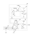
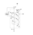
- FIG. 4 is a circuit diagram showing an example configuration of an EVS pixel 300 in the first embodiment of the present technology.
- the logarithmic response unit 320 includes a log transistor 321, a current source transistor 327, and a TIA (TransImpedance Amplifier) 324.
- a log transistor 321, a current source transistor 327, and a TIA (TransImpedance Amplifier) 324 for example, an nMOS (n-channel Metal Oxide Semiconductor) transistor is used as the log transistor 321 and the TIA 324.
- a pMOS (p-channel MOS) transistor is used as the current source transistor 327.
- the log transistor 321 is inserted between the power supply voltage and the photoelectric conversion element 310.
- the current source transistor 327 and the TIA 324 are connected in series between the power supply voltage and a reference voltage (such as a ground voltage).
- connection node between the log transistor 321 and the photoelectric conversion element 310 is connected to the gate of the TIA 324.
- the connection node between the current source transistor 327 and the TIA 324 is connected to the gate of the log transistor 321 and the buffer 330.
- a fixed bias voltage Vblog is applied to the gate of the current source transistor 327.
- the log transistor 321 converts the photocurrent generated by the photoelectric conversion element 310 into a logarithmic voltage.
- the TIA 324 inverts and amplifies the logarithmic voltage. Note that in the figure, the loop circuit consisting of the log transistor 321 and the TIA 324 is one stage, but it can also be two or more stages, as described below.
- the buffer 330 includes a source follower transistor 331 and an nMOS transistor 332.
- an nMOS transistor is used as the source follower transistor.
- the source follower transistor 331 and the nMOS transistor 332 are connected in series between the power supply voltage and the reference voltage.
- the logarithmic voltage Vp from the logarithmic response unit 320 is input to the gate of the source follower transistor 331, and the source of the source follower transistor 331 is connected to the differentiator 340.
- the bias voltage Vbsf generated by the bias voltage generation circuit 216 is input to the gate of the nMOS transistor 332.
- the source follower transistor 331 supplies an output signal corresponding to the logarithmic voltage Vp to the differentiator 340. Furthermore, the nMOS transistor 332 supplies a bias current Ib corresponding to the bias voltage Vbsf.
- the parameter control circuit 215 controls the bias voltage Vbsf according to the illuminance. The details of the control will be described later. Note that the bias voltage Vbsf is an example of the first bias voltage described in the claims.
- Differentiator 340 includes capacitors 341 and 343, pMOS transistor 344, nMOS transistors 342 and 345, and bias switch 346.
- One end of the capacitance 341 is connected to the buffer 330, and the other end is connected to one end of the capacitance 343 and the gate of the pMOS transistor 344.
- a reset signal rst is input to the gate of the nMOS transistor 342, and the source and drain are connected to both ends of the capacitance 343.
- the pMOS transistor 344 and the nMOS transistor 345 are connected in series between the power supply voltage and the reference voltage.
- the other end of the capacitance 343 is connected to the connection point of the pMOS transistor 344 and the nMOS transistor 345.
- a bias voltage from the bias changeover switch 346 is applied to the gate of the nMOS transistor 345 on the reference voltage side, and the connection point of the pMOS transistor 344 and the nMOS transistor 345 is also connected to the comparator 350.
- the nMOS transistor 345 supplies a bias current according to the bias voltage.
- the bias changeover switch 346 selects one of the bias voltages AZ, POS, and NEG according to the selection signal SW from the readout area selection unit 211, and supplies it to the nMOS transistor 345.
- the bias voltage AZ is supplied during auto-zero.
- the bias voltage POS is supplied during the detection period of an on-event, and the bias voltage NEG is supplied during the detection period of an off-event. These bias voltages are assumed to be fixed values.
- the differentiator 340 during the detection period of an on-event, the differentiator 340 generates a differential signal indicating the amount of increase in luminance and outputs it to the comparator 350.
- the differentiator 340 During the detection period of an off-event, the differentiator 340 generates a differential signal indicating the amount of decrease in luminance and outputs it to the comparator 350.
- the differential signal is initialized by the reset signal rst from the readout area selection unit 211.
- Comparator 350 includes a pMOS transistor 351 and an nMOS transistor 352. These pMOS transistor 351 and nMOS transistor 352 are connected in series between the power supply voltage and the reference voltage.
- the differentiated signal from the differentiator 340 is input to the gate of the pMOS transistor 351 on the power supply side.
- a bias voltage Vth the value of which corresponds to a threshold value, is input to the gate of the nMOS transistor 352.
- This bias voltage Vth is assumed to be a fixed value.
- the voltage at the connection point between the pMOS transistor 351 and the nMOS transistor 352 is output to the output circuit 360 as the comparison result.
- the comparator 350 compares the differential signal indicating the amount of increase or decrease in luminance with the value of the bias voltage Vth (i.e., the threshold value), and outputs the comparison result to the output circuit 360.
- the circuits in the solid-state imaging device 200 can also be distributed across multiple semiconductor chips.
- the light receiving chip and the circuit chip are stacked. Then, the photoelectric conversion element 310, the log transistor 321, and the TIA 324 are arranged on the light receiving chip, and the subsequent circuitry from the current source transistor 327 onwards is arranged on the circuit chip.
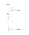
- FIG. 6 is a graph showing an example of frequency characteristics when the bias voltage Vbsf in the first embodiment of the present technology is Vbsf1, which is higher than a predetermined value.
- a shows the frequency characteristics of the logarithmic response unit 320
- b shows the frequency characteristics of the buffer 330
- c shows the frequency characteristics of the entire circuit including the logarithmic response unit 320 and the buffer 330.
- the vertical axis shows the gain
- the horizontal axis shows the frequency.
- the gain is constant in the frequency band below the cutoff frequency, and the gain decreases according to the frequency in the frequency band above the cutoff frequency.
- the cutoff frequency becomes higher as the illuminance increases, and the cutoff frequency when the illuminance is relatively high is denoted by f c_logH , and the cutoff frequency when the illuminance is relatively low is denoted by f c_logL .
- the gain is constant in the frequency band below the cutoff frequency f c_SF1 , and the gain decreases according to the frequency in the frequency band above the cutoff frequency f c_SF1 .
- This cutoff frequency f c_SF1 is constant regardless of the illuminance.
- Vbsf1 is set to a value that makes the cutoff frequency f c_SF1 higher than f c_logH .
- the frequency characteristics of the logarithmic response section 320 with the lower cutoff frequency in other words the narrower frequency band through which signals pass, dominate the entire circuit.
- FIG. 7 is a graph showing an example of frequency characteristics when the bias voltage Vbsf in the first embodiment of the present technology is Vbsf2, which is lower than a predetermined value.
- a shows the frequency characteristics of the logarithmic response unit 320
- b shows the frequency characteristics of the buffer 330
- c shows the frequency characteristics of the entire circuit including the logarithmic response unit 320 and the buffer 330.
- the vertical axis in a, b, and c shows the gain
- the horizontal axis shows the frequency.
- the cutoff frequency of the logarithmic response unit 320 changes depending on the illuminance.
- the cutoff frequency f c_SF2 of the buffer 330 is constant regardless of the illuminance.
- Vbsf2 is set to a value that makes the cutoff frequency f c_SF2 lower than f c_logL .
- the frequency characteristics of the buffer 330 with the narrower frequency band dominate the entire circuit.
- the frequency band can be narrowed by controlling the bias voltage Vbsf to the lower Vbsf2.
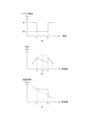
- FIG. 8 is a graph showing an example of bias current, noise, and delay time according to illuminance in the first embodiment of the present technology.
- a is a graph showing an example of the relationship between illuminance and bias current in the buffer 330.
- the vertical axis represents bias current
- the horizontal axis represents illuminance.
- b is a graph showing an example of the relationship between noise generated in a dark state and illuminance.
- the vertical axis of the figure, b indicates the noise BGR (Background Rate), and the horizontal axis indicates the frequency.
- the dashed dotted line indicates the BGR when the bias voltage Vbsf to the buffer 330 is fixed, and the solid line indicates the BGR when the bias voltage Vbsf is controlled so as to generate the bias current of the figure, a.
- C in the figure is a graph showing an example of the relationship between illuminance and the delay time of the EVS pixel 300.
- the vertical axis of c in the figure shows the delay time, and the horizontal axis shows the frequency.
- the dashed dotted line shows the delay time when the bias voltage Vbsf to the buffer 330 is fixed, and the solid line shows the delay time when the bias voltage Vbsf is controlled to generate the bias current of a in the figure.
- the parameter control circuit 215 when the illuminance is within the range of L 1 L to L 1 H , the parameter control circuit 215 generates the bias voltage Vbsf2 and reduces the bias current to Ib2, which is lower than the predetermined value. On the other hand, when the illuminance is outside the range of L 1 L to L 1 H , the parameter control circuit 215 generates the bias voltage Vbsf1 and increases the bias current to Ib1, which is higher than the predetermined value. As described above, by controlling the bias voltage Vbsf to the lower Vbsf2, the frequency band through which the signal passes can be narrowed.
- the parameter control circuit 215 lowering the bias voltage within the range of L 1 L to L 1 H , the noise peak can be suppressed compared to the case where the bias voltage is set to a fixed value. Furthermore, since the peak can be sufficiently suppressed, the frequency band of the logarithmic response unit 320 can also be slightly narrowed. By narrowing the frequency band, the delay time at an illuminance lower than L 1 L can be reduced.
- FIG. 9 is a diagram showing an example of readout control of the EVS pixel 300 in the first embodiment of the present technology.
- the readout region selection unit 211 selects rows in the pixel array unit 213 one by one in sequence, and causes each of the EVS pixels 300 in the row to detect an address event. Note that the readout region selection unit 211 can also select n rows (n is an integer equal to or greater than 2) in sequence.
- the read area selection unit 211 supplies a reset signal rst to that row and switches the bias voltage in the differentiator 340 to AZ.
- the readout area selection unit 211 switches the bias voltage in the differentiator 340 to POS.
- the readout area selection unit 211 switches the bias voltage in the differentiator 340 to NEG.
- the method of reading out row by row in sequence is called the scan method.
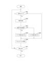
- FIG. 10 is a flowchart showing an example of the operation of the solid-state imaging device 200 in the first embodiment of the present technology. This operation is started, for example, when a specific application for detecting an address event is executed.
- the illuminance meter 214 judges whether the current time is the timing for measuring the illuminance (step S901). The illuminance is measured, for example, at regular intervals. If it is the timing for measuring the illuminance (step S901: Yes), the illuminance meter 214 measures the illuminance (step S902). The parameter control circuit 215 judges whether the measured illuminance is within a predetermined range from L L to L H (step S903). If the illuminance is within the predetermined range (step S903: Yes), the parameter control circuit 215 makes the bias voltage lower than a predetermined value (step S904). On the other hand, if the illuminance is outside the predetermined range (step S903: No), the parameter control circuit 215 makes the bias voltage higher than a predetermined value (step S905).
- step S901 If it is not time to measure the illuminance (step S901: No), or after step S904 or S905, the readout area selection unit 211 detects address events on a row-by-row basis (step S906). After step S906, the readout area selection unit 211 determines whether to end the readout (step S906).
- step S907: No If the readout is not to be ended (step S907: No), the readout area selection unit 211 returns to step S901. On the other hand, if the readout is to be ended (step S907: No), the solid-state imaging element 200 ends the operation for detecting an address event.
- the parameter control circuit 215 controls the bias voltage Vbsf to the buffer 330 according to the illuminance, thereby suppressing noise.
- the parameter control circuit 215 controls the bias voltage Vbsf to the buffer 330, but is not limited to this configuration.
- the parameter control circuit 215 in the first modification of the first embodiment differs from the first embodiment in that it controls the bias voltage to the differentiator 340.
- FIG. 11 is a circuit diagram showing an example of the configuration of an EVS pixel 300 in a first modified example of the first embodiment of the present technology.
- a fixed bias voltage Vbsf is applied to the buffer 330.
- the bias voltage generation circuit 216 generates bias voltages AZ, POS, and NEG for the differentiator 340.
- the parameter control circuit 215 controls the bias voltages POS and NEG according to the illuminance.
- a fixed value is set for the bias voltage AZ.
- the bias voltages POS and NEG are an example of a second bias voltage described in the claims.
- FIG. 12 is a diagram showing an example of bias current, noise, and delay according to illuminance in a first modified example of the first embodiment of the present technology.
- a is a graph showing an example of the relationship between the positive bias current and illuminance according to the bias voltage POS.
- a is a graph showing an example of the relationship between the negative bias current and illuminance according to the bias voltage NEG.
- the vertical axis indicates the bias current
- the horizontal axis indicates the illuminance.
- C in the figure is a graph showing an example of the relationship between noise generated in a dark state and illuminance.
- the vertical axis of c in the figure shows the noise BGR, and the horizontal axis shows the frequency.
- the dashed dotted line shows the BGR when the bias voltages POS and NEG are fixed, and the solid line shows the BGR when the bias voltages POS or NEG are controlled to generate the bias current of a or b in the figure.
- d is a graph showing an example of the relationship between illuminance and the delay time of the EVS pixel 300.
- the vertical axis of d in the figure shows the delay time, and the horizontal axis shows the frequency.
- the dashed dotted line shows the delay time when the bias voltages POS and NEG are fixed, and the solid line shows the delay time when the bias voltage POS or NEG is controlled to generate the bias current of a or b in the figure.
- the parameter control circuit 215 when the illuminance is within the range of L L to L H , the parameter control circuit 215 generates a bias voltage POS2 and reduces the positive bias current to Ip2, which is lower than the predetermined value.
- the parameter control circuit 215 when the illuminance is outside the range of L L to L H , the parameter control circuit 215 generates a bias voltage POS1, which is higher than POS2, and increases the positive bias current to Ip1, which is higher than the predetermined value.
- the parameter control circuit 215 during the detection period of an off event, when the illuminance is within the range of L L to L H , the parameter control circuit 215 generates a bias voltage NEG1 and increases the negative bias current to In1, which is higher than a predetermined value. On the other hand, when the illuminance is outside the range of L L to L H , the parameter control circuit 215 generates a bias voltage NEG2, which is lower than NEG1, and decreases the bias current to In2, which is lower than the predetermined value.
- the delay time becomes longer within the range from L 1 L to L 1 H than when the bias voltage is a fixed value.
- the parameter control circuit 215 can also control the bias voltage Vbsf to the buffer 330 in accordance with the illuminance, in addition to the bias voltages POS and NEG.
- the EVS pixel 300 detects both on-events and off-events, but can also detect only one of them. In this case, the parameter control circuit 215 controls only one of the bias voltages POS and NEG.
- the bias voltages POS and NEG to the differentiator 340 are controlled according to the illuminance, thereby suppressing noise.
- the parameter control circuit 215 controls the bias voltage Vbsf to the buffer 330, but is not limited to this configuration.
- the parameter control circuit 215 in the second modified example of the first embodiment differs from the first embodiment in that it controls the bias voltage to the comparator 350.
- FIG. 13 is a circuit diagram showing an example of the configuration of an EVS pixel 300 in a second modified example of the first embodiment of the present technology.
- a fixed bias voltage Vbsf is applied to the buffer 330.
- the bias voltage generation circuit 216 generates a bias voltage Vth to the comparator 350.
- the parameter control circuit 215 controls the value (threshold) of the bias voltage Vth according to the illuminance.
- the bias voltage Vth is an example of a third bias voltage described in the claims.
- the method for controlling the bias voltage Vth is the same as the method for controlling the bias voltage Vbsf in the first embodiment.
- the parameter control circuit 215 can control the bias voltage Vth to the comparator 350 as well as the bias voltage of at least one of the buffer 330 and the differentiator 340 according to the illuminance.
- the bias voltage Vth to the comparator 350 is controlled according to the illuminance, thereby suppressing noise.
- the parameter control circuit 215 controls the bias voltage Vbsf to the buffer 330, but it is also possible to control parameters other than the bias voltage.
- the parameter control circuit 215 in this second embodiment differs from the first embodiment in that it controls the capacitance value of the logarithmic response unit 320.
- FIG. 14 is a block diagram showing an example of the configuration of a solid-state imaging element 200 in a second embodiment of the present technology.
- the solid-state imaging element 200 in this second embodiment does not include a bias voltage generation circuit 216.
- the parameter control circuit 215 controls the capacitance value of a variable capacitance (not shown) in the EVS pixel 300 according to the illuminance.
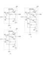
- FIG. 15 is a circuit diagram showing an example of a configuration of a logarithmic response unit 320 in the second embodiment of the present technology.
- a is an example of a logarithmic response unit 320 with a single loop circuit.
- b is an example of a logarithmic response unit 320 with a two-stage loop circuit.
- c is an example of a logarithmic response unit 320 with a three-stage loop circuit.
- the logarithmic response unit 320 in the second embodiment differs from the first embodiment in that it further includes a coupling capacitance 328 and a switch 329.
- the coupling capacitance 328 is inserted between the connection point (in other words, the output node) of the current source transistor 327 and the TIA 324 and the switch 329.
- a fixed bias voltage Vbsf is applied to the downstream buffer 330 (not shown).
- the switch 329 opens and closes the path between the connection point (in other words, the input node) of the log transistor 321 and the photoelectric conversion element 310 and the coupling capacitance 328 under the control of the parameter control circuit 215.
- the parameter control circuit 215 turns the switch 329 on and off depending on the illuminance. For example, when the illuminance is low and below a threshold, the parameter control circuit 215 controls the switch 329 to the off state, and when the illuminance is high and above the threshold, the parameter control circuit 215 turns the switch 329 on and inserts the coupling capacitance 328.
- the loop circuit consisting of the log transistor 321 and the TIA 324 is one stage, but the loop circuit is not limited to one stage.
- log transistor 322 and TIA 325 can be added to form a two-stage loop circuit.
- log transistor 322 is inserted between log transistor 321 and the input node
- TIA 325 is inserted between TIA 324 and a reference voltage (such as a ground voltage).
- the gate of log transistor 322 is connected to the connection point between TIAs 324 and 325, and the gate of TIA 325 is connected to the input node.
- a log transistor 323 and a TIA 326 can be further added to make the loop circuit three stages.
- log transistor 323 is inserted between log transistor 322 and the input node
- TIA 326 is inserted between TIA 325 and the reference voltage.
- the gate of log transistor 323 is connected to the connection point of TIA 325 and 326, and the gate of TIA 326 is connected to the input node.
- the loop circuit can also be four or more stages.
- diode-connected nMOS transistors can be inserted.
- a diode-connected nMOS transistor 322-1 is added between the log transistor 321 and the input node.
- a diode-connected nMOS transistor 323-1 is further added between the nMOS transistor 322-1 and the input node.
- Diode-connected nMOS transistors can also be provided in three or more stages.
- FIG. 17 is a circuit diagram showing an example of the configuration of a logarithmic response unit to which coupling capacitances and switches have been added in the second embodiment of the present technology.
- coupling capacitances 328-1 and 328-2 and switches 329-1 and 329-2 have been added.
- One end of coupling capacitances 328-1 and 328-2 is commonly connected to the output node.
- Switch 329-1 opens and closes the path between the other end of coupling capacitance 328-1 and the input node
- switch 329-2 opens and closes the path between the other end of coupling capacitance 328-2 and the input node.
- the parameter control circuit 215 can open and close each of the multiple switches individually. By controlling these switches, the number of coupling capacitances connected in parallel between the input node and the output node increases or decreases, and the combined capacitance of these changes.
- the coupling capacitance is an example of a variable capacitance as described in the claims.
- the circuit configuration of the logarithmic response unit 320 is not limited to those illustrated in Figures 15 to 17.
- M (M is an integer) switches such as switch 329-1 and M coupling capacitances such as coupling capacitance 328-1 can be inserted between the output node and the reference voltage.
- FIG. 19 is a diagram showing an example of the number of capacitors, noise, and delay according to illuminance in a first modified example of the second embodiment of the present technology.
- a is a graph showing an example of the relationship between the number of capacitors connected in parallel and illuminance.
- the vertical axis of a in the figure shows the number of capacitors, and the horizontal axis shows the illuminance.
- b is a graph showing an example of the relationship between noise occurring in a dark state and illuminance.
- the vertical axis of b in the same figure shows the noise BGR, and the horizontal axis shows the frequency.
- the dashed dotted line shows the BGR when the number of capacitances of the logarithmic response unit 320 is fixed, and the solid line shows the BGR when the number of capacitances is controlled as exemplified in a in the same figure.
- C in the figure is a graph showing an example of the relationship between illuminance and the delay time of the EVS pixel 300.
- the vertical axis of c in the figure shows the delay time, and the horizontal axis shows the frequency.
- the dashed dotted line shows the delay time when the number of capacitances of the logarithmic response unit 320 is fixed, and the solid line shows the delay time when the number of capacitances is controlled as exemplified in a in the figure.
- the parameter control circuit 215 sets the number of capacitors to m1, which is greater than the predetermined value, and increases the capacitance value of the composite capacitor.
- the parameter control circuit 215 sets the number of capacitors to m2, which is less than the predetermined value, and decreases the capacitance value of the composite capacitor. This control makes it possible to suppress noise peaks compared to when the number of capacitors is a fixed value, as shown in FIG. 1B.
- the delay time becomes longer within the range from L L to L H than when the capacitance value is fixed.
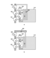
- FIG. 20(a) shows a layout of photoelectric conversion element 310, log transistors 321 and 322, TIAs 324 and 325, switch 329, and coupling capacitance 328.
- Figure 20(b) diffusion capacitance can be added as coupling capacitance 328.
- a MOS capacitance can be added as coupling capacitance 328.
- the coupling capacitance in the logarithmic response unit 320 is variable, but this configuration is not limited to this.
- logarithmic response units 320-1 and 320-2 with different coupling capacitances can be arranged in the EVS pixel 300, and the connection destination of their input nodes can be switched by switches 329-1 and 329-2.
- switch 329-1 opens and closes the path between the input node of logarithmic response unit 320-1 and the photoelectric conversion element 310
- switch 329-2 opens and closes the path between the input node of logarithmic response unit 320-2 and the photoelectric conversion element 310.
- the output nodes of logarithmic response units 320-1 and 320-2 are commonly connected to the subsequent buffer 330.
- the parameter control circuit 215 selects one of logarithmic response units 320-1 and 320-2 according to the illuminance, and controls switches 329-1 and 329-2 to connect it to the photoelectric conversion element 310.
- photoelectric conversion element 310-1 is connected to the input node of logarithmic response unit 320-1
- photoelectric conversion element 310-2 is connected to the input node of logarithmic response unit 320-2
- Switch 329-1 opens and closes the path between the output node of logarithmic response unit 320-1 and buffer 330
- switch 329-2 opens and closes the path between the output node of logarithmic response unit 320-2 and buffer 330.
- Parameter control circuit 215 selects one of logarithmic response units 320-1 and 320-2 depending on the illuminance, and controls switches 329-1 and 329-2 to connect to buffer 330.
- the circuit including the photoelectric conversion element 310-1 and the logarithmic response unit 320-1 functions as one of a pair of subpixels in the EVS pixel 300, and the circuit including the photoelectric conversion element 310-2 and the logarithmic response unit 320-2 functions as the other of the pair of subpixels.
- the parameter control circuit 215 switches the connection destination of two logarithmic response units, but it is also possible to provide three or more logarithmic response units with different coupling capacitances and switch between them.
- the parameter control circuit 215 can also control the bias voltage to at least one of the buffer 330, the differentiator 340, and the comparator 350.
- the parameter control circuit 215 controls the capacitance value of the variable capacitance in the EVS pixel 300 according to the illuminance, thereby suppressing noise.
- the parameter control circuit 215 controls the capacitance value of the variable capacitance in the EVS pixel 300, but is not limited to this configuration.
- the solid-state imaging device 200 in the first modified example of the second embodiment differs from the second embodiment in that it reads out at least one of a plurality of EVS pixels having different coupling capacitances.
- the solid-state imaging element 200 in the first modified example of the second embodiment includes a readout region selection unit 211, a signal generation unit 212, a pixel array unit 213, and a light meter 214.
- a predetermined number of EVS pixels 300-1 and a predetermined number of EVS pixels 300-2 are arranged in a two-dimensional lattice shape in the pixel array unit 213.
- the coupling capacitance C pr1 in the EVS pixel 300-1 is a different value from the coupling capacitance C pr2 in the EVS pixel 300-2.
- the EVS pixels 300-1 and 300-2 are examples of the first and second pixels described in the claims.
- the illuminance meter 214 supplies the measured illuminance to the readout area selection unit 211.
- the readout area selection unit 211 selects and reads out one of the EVS pixels 300-1 and 300-2 depending on the illuminance. For example, when the illuminance is lower than a threshold value, the readout area selection unit 211 selects the EVS pixel 300-1 or 300-2 with the smaller coupling capacitance, and when the illuminance is equal to or higher than the threshold value, the readout area selection unit 211 selects the EVS pixel 300-1 or 300-2 with the larger coupling capacitance. This makes it possible to suppress noise in the same way as in the second embodiment.
- the readout area selection unit 211 can read out all the EVS pixels. In this case, processing according to various illuminance levels can be performed in a downstream circuit.
- FIG. 25 is an example of a circuit diagram of an EVS pixel 300-1 in a first modified example of the second embodiment of the present technology.
- This EVS pixel 300-1 includes a photoelectric conversion element 310, a logarithmic response unit 320, a buffer 330, a differentiator 340, and a comparator 350.
- the coupling capacitance of the logarithmic response unit 320 is a fixed value.
- the bias voltage is a fixed value.
- the circuit configuration of the EVS pixel 300-2 is the same as that of the EVS pixel 300-1, except that the coupling capacitance is different.
- the readout area selection unit 211 selects one of the EVS pixels 300-1 and 300-2, which have different coupling capacitances depending on the illuminance, thereby suppressing noise.
- the parameter control circuit 215 controls the capacitance value of the variable capacitance in the EVS pixel 300 in response to the illuminance, but the capacitance value can also be controlled in response to a measured value other than the illuminance.
- the solid-state imaging element 200 in the second modified example of the second embodiment differs from the second embodiment in that it measures a voltage instead of the illuminance and controls the capacitance value of the variable capacitance in response to the voltage value.
- FIG. 26 is an example of a circuit diagram of an EVS pixel 300 in a second modified example of the second embodiment of the present technology.
- the illuminometer 214 is not arranged in the solid-state imaging element 200.
- a voltmeter 371 and a parameter control circuit 215 are further arranged in the pixel 300.
- the circuit configuration of the logarithmic response unit 320 in the second modified example of the second embodiment is the same as in the second embodiment.
- the voltmeter 371 measures the voltage at the output node of the logarithmic response unit 320 and supplies the measured value to the parameter control circuit 215.
- the voltmeter 371 is an example of a measurement unit described in the claims.
- the parameter control circuit 215 controls the capacitance value of the variable capacitance in the logarithmic response unit 320 according to the voltage value. For example, when the voltage value is lower than a threshold value, the parameter control circuit 215 controls the switch 329 to the off state, and when the voltage value is equal to or higher than the threshold value, the parameter control circuit 215 controls the switch 329 to the on state, inserting the coupling capacitance 328. This suppresses noise.
- the parameter control circuit 215 controls the variable capacitance for each EVS pixel 300 according to its voltage value, but is not limited to this control.
- the parameter control circuit 215 can obtain statistics (average or sum) of the voltage values of all pixels, and control the variable capacitance of each of all pixels according to the statistics.
- the parameter control circuit 215 can obtain statistics (average or sum) of the voltage values of the EVS pixels 300 in each area, and control the variable capacitance in the area according to the statistics.
- the parameter control circuit 215 controls the capacitance value of the variable capacitance in the EVS pixel 300 according to the voltage value, thereby suppressing noise.
- the parameter control circuit 215 controls the capacitance value of the variable capacitance in the EVS pixel 300 in response to the illuminance, but the capacitance value can also be controlled in response to a measured value other than the illuminance.
- the solid-state imaging device 200 in the third modified example of the second embodiment differs from the second embodiment in that it measures a current instead of the illuminance and controls the capacitance value of the variable capacitance in response to the current value.
- FIG. 27 is an example of a circuit diagram of an EVS pixel 300 in a third modified example of the second embodiment of the present technology.
- the illuminometer 214 is not arranged in the solid-state imaging element 200.
- an ammeter 372 and a parameter control circuit 215 are further arranged in the pixel 300.
- the circuit configuration of the logarithmic response unit 320 in the third modified example of the second embodiment is the same as in the second embodiment.
- the ammeter 372 measures the current flowing through the logarithmic response unit 320 and supplies the measured value to the parameter control circuit 215.
- the ammeter 372 is an example of a measurement unit described in the claims.
- the parameter control circuit 215 controls the capacitance value of the variable capacitance in the logarithmic response unit 320 according to the current value. For example, when the current value is smaller than a threshold value, the parameter control circuit 215 controls the switch 329 to the off state, and when the current value is equal to or greater than the threshold value, the parameter control circuit 215 controls the switch 329 to the on state, inserting the coupling capacitance 328. This suppresses noise.
- the parameter control circuit 215 controls the variable capacitance for each EVS pixel 300 according to its current value, but is not limited to this control.
- the parameter control circuit 215 can obtain statistics (average or total) of the current values of all pixels, and control the variable capacitance of each of all pixels according to the statistics.
- the parameter control circuit 215 can obtain statistics (average or total) of the current values of the EVS pixels 300 in each area, and control the variable capacitance within the area according to the statistics.
- the parameter control circuit 215 controls the capacitance value of the variable capacitance in the EVS pixel 300 according to the current value, thereby suppressing noise.
- the illuminometer 214 is arranged outside the pixel array section 213, but this is not limited to the configuration.
- the solid-state imaging device 200 in the third embodiment differs from the first embodiment in that a part of the illuminometer is arranged inside the pixel array section 213.
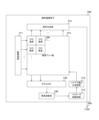
- FIG. 28 is a block diagram showing an example of the configuration of a solid-state imaging device 200 in a third embodiment of the present technology.
- the solid-state imaging device 200 in this third embodiment differs from the first embodiment in that it further includes a driving unit 217, and includes a predetermined number of light receiving units 220, a column ADC 230, and an illuminance calculation unit 240 instead of the illuminometer 214.
- a predetermined number of light receiving sections 220 are arranged in the pixel array section 213. Each of these light receiving sections 220 can be used as a gradation pixel that generates a gradation signal. For example, two of the four pixels in two rows and two columns in the pixel array section 213 are replaced with light receiving sections 220 (in other words, gradation pixels).
- the ratio of the number of pixels and the area of the gradation pixels to the EVS pixels 300 is not limited to 1:1.
- the number of pixels of the gradation pixels can be made greater than the EVS pixels 300, and the area of the gradation pixels can be made smaller than that of the EVS pixels 300.
- the driving unit 217 drives each of the light receiving units 220.
- the light receiving units 220 generate analog signals corresponding to the luminance and supply them to the column ADC 230.
- the column ADC 230 converts the analog signals for each column into digital signals and supplies them to the illuminance calculation unit 240.
- the illuminance calculation unit 240 calculates the illuminance from the digital signal and supplies it to the parameter control circuit 215.
- the column ADC 230 can also output data that is an array of digital signals as image data.
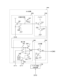
- FIG. 29 is a circuit diagram showing an example configuration of the light receiving unit 220 and the column ADC 230 in the third embodiment of the present technology.
- the light receiving unit 220 includes a photoelectric conversion element 221 and an analog signal generation circuit 222.
- the analog signal generation circuit 222 includes a transfer transistor 223, a reset transistor 224, a floating diffusion layer 225, an amplification transistor 226, and a selection transistor 227.
- the photoelectric conversion element 221 generates electric charges by photoelectric conversion.
- the photoelectric conversion element 310 in the EVS pixel 300 is an example of a first photoelectric conversion element described in the claims
- the photoelectric conversion element 221 is an example of a second photoelectric conversion element described in the claims.
- the transfer transistor 223 transfers charge from the photoelectric conversion element 221 to the floating diffusion layer 225 in accordance with a transfer signal TRG from the drive unit 217.
- the reset transistor 224 initializes the floating diffusion layer 225 in accordance with a reset signal RST from the drive unit 217.
- the amplification transistor 226 amplifies the voltage of the floating diffusion layer 225 to generate an analog signal.
- the selection transistor 227 supplies an analog signal to a vertical signal line VSL in accordance with a selection signal SEL from the drive unit 217.
- the vertical signal line VSL is wired for each column of the light receiving unit 220.
- the column ADC 230 includes an ADC 231 and a load MOS transistor 232 for each column of the light receiving section 220.
- the ADC 231 converts an analog signal from the corresponding vertical signal line VSL into a digital signal and supplies it to the illuminance calculation section 240.
- a single-slope type ADC is used as the ADC 231.
- the load MOS transistor 232 supplies a constant current.
- the illuminance calculation unit 240 calculates the statistics (average or sum) of the digital signal values from the light receiving unit 220 within the photometric range, and supplies this value to the parameter control circuit 215 as illuminance.
- the circuit including all of the analog signal generating circuits 222, the column ADC 230, and the illuminance calculation unit 240 functions as an illuminance meter 250.
- the illuminance of the pixel array section 213 can be measured more accurately than in the first embodiment in which the illuminometer 214 is arranged outside the pixel array section 213.
- the EVS pixels 300 can be arranged at a constant interval in the pixel array section 213.
- the EVS pixel is arranged at the bottom right, and the light receiving section 220 is arranged in the remaining space.
- first and second variations of the first embodiment and the second embodiment can be applied to the third embodiment.
- a part of the illuminometer 250 is disposed in the pixel array section 213, so that the illuminance of the pixel array section 213 can be accurately measured.
- a photoelectric conversion element is disposed in each of the light receiving section 220 and the EVS pixel 300, but this configuration may result in an insufficient light receiving area for each pixel.
- the solid-state imaging device 200 in the first modified example of the third embodiment differs from the first embodiment in that the light receiving section 220 and the EVS pixel 300 share one photoelectric conversion element.
- FIG. 31 is a block diagram showing an example of the configuration of a solid-state imaging element 200 in a first modified example of the third embodiment of the present technology.
- the solid-state imaging element 200 in the first modified example of the third embodiment differs from the third embodiment in that a predetermined number of shared blocks 400 are arranged in the pixel array section 213.
- FIG. 32 is a circuit diagram showing an example configuration of a shared block 400 in a first modified example of the third embodiment of the present technology.
- the shared block 400 includes a light receiving unit 220, an OFG transistor 305, a logarithmic response unit 320, a buffer 330, a differentiator 340, a comparator 350, and an output circuit 360.
- the buffer 330, the differentiator 340, the comparator 350, and the output circuit 360 are omitted.
- the OFG transistor 305 opens and closes the path between the photoelectric conversion element 221 in the light receiving unit 220 and the logarithmic response unit 320 according to a control signal OFG from the readout area selection unit 211.
- the circuit consisting of the photoelectric conversion element 221, the OFG transistor 305, the logarithmic response unit 320, the buffer 330, the differentiator 340, the comparator 350, and the output circuit 360 functions as the EVS pixel 300.
- the light receiving unit 220 and the EVS pixel 300 share one photoelectric conversion element 221.
- the transfer transistor 223 When measuring illuminance or generating a gradation signal, the transfer transistor 223 is controlled to the on state, and the OFG transistor 305 is controlled to the off state.
- the transfer transistor 223 when detecting an address event, the transfer transistor 223 is controlled to the off state, and the OFG transistor 305 is controlled to the on state.
- the light receiving section 220 and the EVS pixel 300 share the photoelectric conversion element 221, which makes it possible to increase the light receiving area per pixel compared to a case in which a photoelectric conversion element is disposed in each of the light receiving section 220 and the EVS pixel 300.
- first and second variations of the first embodiment and the second embodiment can be applied to the first variation of the third embodiment.
- the light receiving section 220 and the EVS pixel 300 share one photoelectric conversion element 221, so the light receiving area per pixel can be made larger than in the third embodiment.
- the light receiving unit 220 is disposed in the pixel array unit 213, but the present invention is not limited to this configuration.
- the solid-state imaging device 200 in the second modified example of the third embodiment differs from the third embodiment in that the circuit scale of the illuminometer 250 is reduced.
- FIG. 33 is a block diagram showing an example of the configuration of a solid-state imaging element 200 in a second modified example of the third embodiment of the present technology.
- the solid-state imaging element 200 in the second modified example of the third embodiment differs from the third embodiment in that only EVS pixels 300 are arranged in the pixel array section 213.
- FIG. 34 is a circuit diagram showing an example configuration of an illuminometer 250 in a second modified example of the third embodiment of the present technology.
- R is an integer
- R analog signal generation circuits 222 are arranged for each column in the pixel array section 213.
- Each analog signal generation circuit 222 includes a changeover switch 228.
- the rth changeover switch 228 (r is an integer from 1 to R) is arranged in the rth row.
- the changeover switch 228 connects the power supply node of the logarithmic response unit 320 in the corresponding EVS pixel 300 to the vertical signal line VSL according to the control of the readout area selection unit 211.
- the changeover switch 228 is controlled to the ON state during the period in which the illuminance is measured, and the changeover switch 228 is controlled to the OFF state during the period in which an address event is detected.
- first and second variations of the first embodiment and the second embodiment can be applied to the second variation of the third embodiment.
- the technology according to the present disclosure can be applied to various products.
- the technology according to the present disclosure may be realized as a device mounted on any type of moving body such as an automobile, an electric vehicle, a hybrid electric vehicle, a motorcycle, a bicycle, a personal mobility device, an airplane, a drone, a ship, or a robot.
- FIG. 35 is a block diagram showing a schematic configuration example of a vehicle control system, which is an example of a mobile object control system to which the technology disclosed herein can be applied.
- the vehicle control system 12000 includes a plurality of electronic control units connected via a communication network 12001.
- the vehicle control system 12000 includes a drive system control unit 12010, a body system control unit 12020, an outside vehicle information detection unit 12030, an inside vehicle information detection unit 12040, and an integrated control unit 12050.
- Also shown as functional components of the integrated control unit 12050 are a microcomputer 12051, an audio/video output unit 12052, and an in-vehicle network I/F (interface) 12053.
- the drive system control unit 12010 controls the operation of devices related to the drive system of the vehicle according to various programs.
- the drive system control unit 12010 functions as a control device for a drive force generating device for generating the drive force of the vehicle, such as an internal combustion engine or a drive motor, a drive force transmission mechanism for transmitting the drive force to the wheels, a steering mechanism for adjusting the steering angle of the vehicle, and a braking device for generating a braking force for the vehicle.
- the body system control unit 12020 controls the operation of various devices installed in the vehicle body according to various programs.
- the body system control unit 12020 functions as a control device for a keyless entry system, a smart key system, a power window device, or various lamps such as headlamps, tail lamps, brake lamps, turn signals, and fog lamps.
- radio waves or signals from various switches transmitted from a portable device that replaces a key can be input to the body system control unit 12020.
- the body system control unit 12020 accepts the input of these radio waves or signals and controls the vehicle's door lock device, power window device, lamps, etc.
- the outside-vehicle information detection unit 12030 detects information outside the vehicle equipped with the vehicle control system 12000.
- the image capturing unit 12031 is connected to the outside-vehicle information detection unit 12030.
- the outside-vehicle information detection unit 12030 causes the image capturing unit 12031 to capture images outside the vehicle and receives the captured images.
- the outside-vehicle information detection unit 12030 may perform object detection processing or distance detection processing for people, cars, obstacles, signs, characters on the road surface, etc. based on the received images.
- the imaging unit 12031 is an optical sensor that receives light and outputs an electrical signal according to the amount of light received.
- the imaging unit 12031 can output the electrical signal as an image, or as distance measurement information.
- the light received by the imaging unit 12031 may be visible light, or may be invisible light such as infrared light.
- the in-vehicle information detection unit 12040 detects information inside the vehicle.
- a driver state detection unit 12041 that detects the state of the driver is connected.
- the driver state detection unit 12041 includes, for example, a camera that captures an image of the driver, and the in-vehicle information detection unit 12040 may calculate the driver's degree of fatigue or concentration based on the detection information input from the driver state detection unit 12041, or may determine whether the driver is dozing off.
- the microcomputer 12051 can calculate control target values for the driving force generating device, steering mechanism, or braking device based on information inside and outside the vehicle acquired by the outside-vehicle information detection unit 12030 or the inside-vehicle information detection unit 12040, and output control commands to the drive system control unit 12010.
- the microcomputer 12051 can perform cooperative control aimed at realizing the functions of an Advanced Driver Assistance System (ADAS), including vehicle collision avoidance or impact mitigation, following driving based on the distance between vehicles, maintaining vehicle speed, vehicle collision warning, or vehicle lane departure warning.
- ADAS Advanced Driver Assistance System
- the microcomputer 12051 can also perform cooperative control for the purpose of autonomous driving, which allows the vehicle to travel autonomously without relying on the driver's operation, by controlling the driving force generating device, steering mechanism, braking device, etc. based on information about the surroundings of the vehicle acquired by the outside vehicle information detection unit 12030 or the inside vehicle information detection unit 12040.
- the microcomputer 12051 can also output control commands to the body system control unit 12020 based on information outside the vehicle acquired by the outside information detection unit 12030. For example, the microcomputer 12051 can control the headlamps according to the position of a preceding vehicle or an oncoming vehicle detected by the outside information detection unit 12030, and perform cooperative control aimed at preventing glare, such as switching from high beams to low beams.
- the audio/image output unit 12052 transmits at least one output signal of audio and image to an output device capable of visually or audibly notifying the occupants of the vehicle or the outside of the vehicle of information.
- an audio speaker 12061, a display unit 12062, and an instrument panel 12063 are exemplified as output devices.
- the display unit 12062 may include, for example, at least one of an on-board display and a head-up display.
- FIG. 36 shows an example of the installation position of the imaging unit 12031.
- the imaging unit 12031 includes imaging units 12101, 12102, 12103, 12104, and 12105.
- the imaging units 12101, 12102, 12103, 12104, and 12105 are provided, for example, at the front nose, side mirrors, rear bumper, back door, and upper part of the windshield inside the vehicle cabin of the vehicle 12100.
- the imaging unit 12101 provided at the front nose and the imaging unit 12105 provided at the upper part of the windshield inside the vehicle cabin mainly acquire images of the front of the vehicle 12100.
- the imaging units 12102 and 12103 provided at the side mirrors mainly acquire images of the sides of the vehicle 12100.
- the imaging unit 12104 provided at the rear bumper or back door mainly acquires images of the rear of the vehicle 12100.
- the imaging unit 12105 provided at the upper part of the windshield inside the vehicle cabin is mainly used to detect leading vehicles, pedestrians, obstacles, traffic lights, traffic signs, lanes, etc.
- FIG. 36 shows an example of the imaging ranges of the imaging units 12101 to 12104.
- Imaging range 12111 indicates the imaging range of the imaging unit 12101 provided on the front nose
- imaging ranges 12112 and 12113 indicate the imaging ranges of the imaging units 12102 and 12103 provided on the side mirrors, respectively
- imaging range 12114 indicates the imaging range of the imaging unit 12104 provided on the rear bumper or back door.
- an overhead image of the vehicle 12100 viewed from above is obtained by superimposing the image data captured by the imaging units 12101 to 12104.
- At least one of the imaging units 12101 to 12104 may have a function of acquiring distance information.
- at least one of the imaging units 12101 to 12104 may be a stereo camera consisting of multiple imaging elements, or an imaging element having pixels for phase difference detection.
- the microcomputer 12051 can obtain the distance to each solid object within the imaging ranges 12111 to 12114 and the change in this distance over time (relative speed with respect to the vehicle 12100) based on the distance information obtained from the imaging units 12101 to 12104, and can extract as a preceding vehicle, in particular, the closest solid object on the path of the vehicle 12100 that is traveling in approximately the same direction as the vehicle 12100 at a predetermined speed (e.g., 0 km/h or faster). Furthermore, the microcomputer 12051 can set the inter-vehicle distance that should be maintained in advance in front of the preceding vehicle, and perform automatic braking control (including follow-up stop control) and automatic acceleration control (including follow-up start control). In this way, cooperative control can be performed for the purpose of automatic driving, which runs autonomously without relying on the driver's operation.
- automatic braking control including follow-up stop control
- automatic acceleration control including follow-up start control
- the microcomputer 12051 classifies and extracts three-dimensional object data on three-dimensional objects, such as two-wheeled vehicles, ordinary vehicles, large vehicles, pedestrians, utility poles, and other three-dimensional objects, based on the distance information obtained from the imaging units 12101 to 12104, and can use the data to automatically avoid obstacles.
- the microcomputer 12051 distinguishes obstacles around the vehicle 12100 into obstacles that are visible to the driver of the vehicle 12100 and obstacles that are difficult to see.
- the microcomputer 12051 determines the collision risk, which indicates the risk of collision with each obstacle, and when the collision risk is equal to or exceeds a set value and there is a possibility of a collision, it can provide driving assistance for collision avoidance by outputting an alarm to the driver via the audio speaker 12061 or the display unit 12062, or by performing forced deceleration or avoidance steering via the drive system control unit 12010.
- At least one of the imaging units 12101 to 12104 may be an infrared camera that detects infrared rays.
- the microcomputer 12051 can recognize a pedestrian by determining whether or not a pedestrian is present in the image captured by the imaging units 12101 to 12104. The recognition of such a pedestrian is performed, for example, by a procedure of extracting feature points in the image captured by the imaging units 12101 to 12104 as infrared cameras, and a procedure of performing pattern matching processing on a series of feature points that indicate the contour of an object to determine whether or not it is a pedestrian.
- the audio/image output unit 12052 controls the display unit 12062 to superimpose a rectangular contour line for emphasis on the recognized pedestrian.
- the audio/image output unit 12052 may also control the display unit 12062 to display an icon or the like indicating a pedestrian at a desired position.
- the technology disclosed herein can be applied to, for example, the imaging unit 12031.
- the imaging device 100 in FIG. 1 can be applied to the imaging unit 12031.
- the technology disclosed herein it is possible to suppress noise and obtain higher quality data.
- the present technology can also be configured as follows. (1) a light meter for measuring light intensity; a detection pixel for detecting whether or not a change in luminance has exceeded a predetermined threshold; a parameter control circuit for controlling a parameter of the detection pixel in response to the measured illuminance.
- the detection pixel is A photoelectric conversion element that generates a photocurrent; a logarithmic response unit that converts the photocurrent into a logarithmic voltage; a buffer for outputting an output signal corresponding to the logarithmic voltage; a differentiator for differentiating the output signal to provide a differentiated signal;
- the solid-state imaging device according to (1), further comprising a comparator for comparing the differential signal with a predetermined threshold value.
- the bias voltage includes a first bias voltage;
- the bias voltage generating circuit supplies the first bias voltage to the buffer.
- the bias voltage includes a second bias voltage;
- the bias voltage generating circuit supplies the second bias voltage to the differentiator.
- the bias voltage includes a third bias voltage;
- the detection pixel includes a variable capacitance
- the detection pixels are arranged in a pixel array section, The solid-state imaging device according to any one of (1) to (10), wherein the illuminometer is disposed outside the pixel array portion.
- the illuminometer comprises: an analog signal generating circuit for generating an analog signal according to the luminance; an analog-to-digital converter for converting the analog signal into a digital signal; an illuminance calculation unit that calculates an illuminance from the digital signal;
- the solid-state imaging device according to any one of (1) to (10), wherein the analog signal generating circuit and the detection pixels are arranged in a pixel array section.
- the detection pixel includes a first photoelectric conversion element
- the analog signal generating circuit includes: a transfer transistor that transfers charges from the second photoelectric conversion element to the floating diffusion layer; a reset transistor for initializing the floating diffusion layer; an amplifying transistor that amplifies a voltage of the floating diffusion layer to generate the analog signal;
- the detection pixel includes a photoelectric conversion element
- the analog signal generating circuit includes: a transfer transistor that transfers charges from the photoelectric conversion element to a floating diffusion layer; a reset transistor for initializing the floating diffusion layer; an amplifying transistor that amplifies a voltage of the floating diffusion layer to generate the analog signal;
- the detection pixel is A photoelectric conversion element that generates a photocurrent; a logarithmic response unit that converts the photocurrent into a logarithmic voltage;
- (16) A procedure for measuring illuminance; detecting whether or not a change in luminance has exceeded a predetermined threshold; and a step of controlling a parameter of the detection pixel in response to the measured illuminance.
- a measurement unit that measures a value of the electrical signal and outputs the measurement value; a detection pixel for detecting whether or not a change in luminance has exceeded a predetermined threshold; a parameter control circuit that controls a parameter of the detection pixel in response to the measurement value.
- the measurement value is a value of a current flowing through the detection pixel.
- the measurement value is a voltage value of a predetermined node in the detection pixel.
- a light meter for measuring light intensity; a first pixel having a first capacitance; a second pixel having a second capacitance; a readout area selection section that reads out one of the first and second pixels in accordance with the illuminance.
- Imaging device 110 Imaging lens 120 Recording section 130 Control section 200 Solid-state imaging element 211 Readout area selection section 212 Signal generation section 213 Pixel array section 214, 250 Illuminometer 215 Parameter control circuit 216 Bias voltage generation circuit 217 Driving section 220 Light receiving section 221, 310, 310-1, 310-2 Photoelectric conversion element 222 Analog signal generation circuit 223 Transfer transistor 224 Reset transistor 225 Floating diffusion layer 226 Amplification transistor 227 Selection transistor 228 Changeover switch 230 Column ADC 231 A.D.C.
Landscapes
- Engineering & Computer Science (AREA)
- Multimedia (AREA)
- Signal Processing (AREA)
- Transforming Light Signals Into Electric Signals (AREA)
Abstract
Description
本技術は、固体撮像素子に関する。詳しくは、輝度の変化を検出する固体撮像素子、および、その制御方法に関する。 This technology relates to solid-state imaging devices. More specifically, it relates to solid-state imaging devices that detect changes in luminance, and to a method of controlling the same.
従来より、垂直同期信号などの同期信号に同期して画像データを撮像する同期型の固体撮像素子が、撮像装置などにおいて用いられている。この一般的な同期型の固体撮像素子では、同期信号の周期(例えば、1/60秒)ごとにしか画像データを取得することができない。そのため、交通やロボットなどに関する分野において、より高速な処理が要求された場合に対応することが困難になる。そこで、画素アドレスごとに、その画素の輝度の変化量が所定の閾値を超えたか否かにより、アドレスイベントをリアルタイムに検出する非同期型の固体撮像素子が提案されている(例えば、非特許文献1参照。)。このように、画素毎にアドレスイベントを検出する固体撮像素子は、EVS(Event-based Vision Sensor)や、DVS(Dynamic Vision Sensor)と呼ばれる。このEVSでは、輝度の変化量を求めるためにバッファや微分器が用いられ、その変化量と閾値との比較のために比較器が用いられている。 Conventionally, synchronous solid-state imaging elements that capture image data in synchronization with a synchronization signal such as a vertical synchronization signal have been used in imaging devices. This general synchronous solid-state imaging element can only capture image data at every synchronization signal period (e.g., 1/60 seconds). This makes it difficult to respond to requests for faster processing in fields such as transportation and robots. Therefore, an asynchronous solid-state imaging element has been proposed that detects address events in real time for each pixel address based on whether or not the amount of change in luminance of that pixel exceeds a predetermined threshold (see, for example, Non-Patent Document 1). A solid-state imaging element that detects address events for each pixel in this way is called an EVS (Event-based Vision Sensor) or a DVS (Dynamic Vision Sensor). In this EVS, a buffer and a differentiator are used to determine the amount of change in luminance, and a comparator is used to compare the amount of change with a threshold.
上述の従来技術では、バッファ、微分器や比較器を用いることにより、アドレスイベントの検出を図っている。しかしながら、上述のEVSでは、暗状態で回路内にノイズが生じることがある。回路内のバイアス電流や容量値を制御すれば、ノイズが低減することもあるが、その一方で遅延時間が長くなるおそれがある。このように、上述のEVSでは、ノイズを抑制することが困難である。 In the above-mentioned conventional technology, address events are detected by using a buffer, a differentiator, and a comparator. However, in the above-mentioned EVS, noise may occur within the circuit in a dark state. Although the noise may be reduced by controlling the bias current and capacitance value within the circuit, this may result in an increase in the delay time. As such, it is difficult to suppress noise with the above-mentioned EVS.
本技術はこのような状況に鑑みて生み出されたものであり、アドレスイベントを検出する固体撮像素子において、ノイズを抑制することを目的とする。 This technology was developed in light of these circumstances, and aims to suppress noise in solid-state imaging elements that detect address events.
本技術は、上述の問題点を解消するためになされたものであり、その第1の側面は、照度を測定する照度計と、輝度の変化量が所定の閾値を超えたか否かを検出する検出画素と、上記測定された照度に応じて上記検出画素のパラメータを制御するパラメータ制御回路とを具備する固体撮像素子である。これにより、ノイズが抑制されるという作用をもたらす。 This technology has been made to solve the above-mentioned problems, and its first aspect is a solid-state imaging device that includes an illuminometer that measures illuminance, a detection pixel that detects whether the amount of change in luminance has exceeded a predetermined threshold, and a parameter control circuit that controls the parameters of the detection pixel according to the measured illuminance. This has the effect of suppressing noise.
また、この第1の側面において、上記検出画素は、光電流を生成する光電変換素子と、上記光電流を対数電圧に変換する対数応答部と、上記対数電圧に応じた出力信号を出力するバッファと、上記出力信号を微分して微分信号を供給する微分器と、上記微分信号と所定の閾値とを比較する比較器とを備えてもよい。これにより、アドレスイベントが検出されるという作用をもたらす。 In addition, in this first aspect, the detection pixel may include a photoelectric conversion element that generates a photocurrent, a logarithmic response unit that converts the photocurrent into a logarithmic voltage, a buffer that outputs an output signal corresponding to the logarithmic voltage, a differentiator that differentiates the output signal and supplies a differentiated signal, and a comparator that compares the differentiated signal with a predetermined threshold. This provides the effect of detecting an address event.
また、この第1の側面において、上記パラメータ制御回路の制御に従ってバイアス電圧を生成して上記検出画素に供給するバイアス電圧生成回路をさらに具備し、上記パラメータは、上記バイアス電圧を含むものであってもよい。これにより、バイアス電圧の制御によってノイズが抑制されるという作用をもたらす。 In addition, in this first aspect, a bias voltage generation circuit may be further provided that generates a bias voltage according to the control of the parameter control circuit and supplies the bias voltage to the detection pixel, and the parameter may include the bias voltage. This provides the effect of suppressing noise by controlling the bias voltage.
また、この第1の側面において、上記バイアス電圧は、第1のバイアス電圧を含み、上記バイアス電圧生成回路は、上記バッファに上記第1のバイアス電圧を供給してもよい。これにより、バッファへのバイアス電圧の制御によってノイズが抑制されるという作用をもたらす。 Furthermore, in this first aspect, the bias voltage may include a first bias voltage, and the bias voltage generation circuit may supply the first bias voltage to the buffer. This provides the effect of suppressing noise by controlling the bias voltage to the buffer.
また、この第1の側面において、上記バイアス電圧は、第2のバイアス電圧を含み、上記バイアス電圧生成回路は、上記微分器に上記第2のバイアス電圧を供給してもよい。これにより、微分器へのバイアス電圧の制御によってノイズが抑制されるという作用をもたらす。 Furthermore, in this first aspect, the bias voltage may include a second bias voltage, and the bias voltage generation circuit may supply the second bias voltage to the differentiator. This provides the effect of suppressing noise by controlling the bias voltage to the differentiator.
また、この第1の側面において、上記バイアス電圧は、第3のバイアス電圧を含み、上記バイアス電圧生成回路は、上記比較器に上記閾値を示す上記第3のバイアス電圧を供給してもよい。これにより、比較器へのバイアス電圧の制御によってノイズが抑制されるという作用をもたらす。 In addition, in this first aspect, the bias voltage may include a third bias voltage, and the bias voltage generation circuit may supply the third bias voltage indicating the threshold value to the comparator. This provides the effect of suppressing noise by controlling the bias voltage to the comparator.
また、この第1の側面において、上記検出画素は、可変容量を含み、上記パラメータは、上記可変容量の容量値を含むものであってもよい。これにより、容量値の制御によってノイズが抑制されるという作用をもたらす。 In addition, in this first aspect, the detection pixel may include a variable capacitance, and the parameter may include a capacitance value of the variable capacitance. This provides the effect of suppressing noise by controlling the capacitance value.
また、この第1の側面において、上記可変容量は、上記対数応答部の入力ノードと出力ノードとの間に挿入されてもよい。これにより、容量値の制御によってノイズが抑制されるという作用をもたらす。 In addition, in this first aspect, the variable capacitance may be inserted between the input node and the output node of the logarithmic response unit. This provides the effect of suppressing noise by controlling the capacitance value.
また、この第1の側面において、上記可変容量は、上記対数応答部の出力ノードと所定の基準電圧との間に挿入されてもよい。これにより、容量値の制御によってノイズが抑制されるという作用をもたらす。 In addition, in this first aspect, the variable capacitance may be inserted between the output node of the logarithmic response unit and a predetermined reference voltage. This provides the effect of suppressing noise by controlling the capacitance value.
また、この第1の側面において、上記パラメータ制御回路は、上記照度が所定範囲内の場合と上記照度が上記所定範囲外の場合とで異なる値に上記パラメータを制御してもよい。これにより、ノイズのピークが抑制されるという作用をもたらす。 In addition, in this first aspect, the parameter control circuit may control the parameters to different values when the illuminance is within a predetermined range and when the illuminance is outside the predetermined range. This has the effect of suppressing noise peaks.
また、この第1の側面において、上記検出画素は、画素アレイ部に配列され、上記照度計は、上記画素アレイ部の外部に配置されてもよい。これにより、画素アレイ部に検出画素のみが配列されるという作用をもたらす。 Furthermore, in this first aspect, the detection pixels may be arranged in a pixel array section, and the illuminometer may be disposed outside the pixel array section. This provides the effect of only having the detection pixels arranged in the pixel array section.
また、この第1の側面において、上記照度計は、輝度に応じたアナログ信号を生成するアナログ信号生成回路と、上記アナログ信号をデジタル信号に変換するアナログデジタル変換器と、上記デジタル信号から照度を演算する照度演算部とを備え、上記アナログ信号生成回路および上記検出画素は、画素アレイ部に配列されてもよい。これにより、照度の測定精度が向上するという作用をもたらす。 In addition, in this first aspect, the illuminance meter may include an analog signal generation circuit that generates an analog signal corresponding to the luminance, an analog-to-digital converter that converts the analog signal into a digital signal, and an illuminance calculation unit that calculates the illuminance from the digital signal, and the analog signal generation circuit and the detection pixels may be arranged in a pixel array unit. This provides the effect of improving the accuracy of illuminance measurement.
また、この第1の側面において、上記検出画素は、第1の光電変換素子を備え、上記アナログ信号生成回路は、第2の光電変換素子から浮遊拡散層へ電荷を転送する転送トランジスタと、上記浮遊拡散層を初期化するリセットトランジスタと、上記浮遊拡散層の電圧を増幅して上記アナログ信号を生成する増幅トランジスタと、選択信号に従って上記アナログ信号を上記アナログデジタル変換器へ供給する選択トランジスタとを備えてもよい。これにより、階調信号が生成されるという作用をもたらす。 In addition, in this first aspect, the detection pixel may include a first photoelectric conversion element, and the analog signal generation circuit may include a transfer transistor that transfers charge from the second photoelectric conversion element to a floating diffusion layer, a reset transistor that initializes the floating diffusion layer, an amplification transistor that amplifies the voltage of the floating diffusion layer to generate the analog signal, and a selection transistor that supplies the analog signal to the analog-to-digital converter in accordance with a selection signal. This provides the effect of generating a gradation signal.
また、この第1の側面において、上記検出画素は、光電変換素子を備え、上記アナログ信号生成回路は、上記光電変換素子から浮遊拡散層へ電荷を転送する転送トランジスタと、上記浮遊拡散層を初期化するリセットトランジスタと、上記浮遊拡散層の電圧を増幅して上記アナログ信号を生成する増幅トランジスタと、選択信号に従って上記アナログ信号を上記アナログデジタル変換器へ供給する選択トランジスタとを備えてもよい。これにより、画素当たりの受光面積が広くなるという作用をもたらす。 In addition, in this first aspect, the detection pixel may include a photoelectric conversion element, and the analog signal generation circuit may include a transfer transistor that transfers charge from the photoelectric conversion element to a floating diffusion layer, a reset transistor that initializes the floating diffusion layer, an amplification transistor that amplifies the voltage of the floating diffusion layer to generate the analog signal, and a selection transistor that supplies the analog signal to the analog-digital converter in accordance with a selection signal. This provides the effect of increasing the light receiving area per pixel.
また、この第1の側面において、上記検出画素は、光電流を生成する光電変換素子と、上記光電流を対数電圧に変換する対数応答部とを備え、上記アナログ信号生成回路は、上記対数応答部の電源ノードと上記アナログデジタル変換器とを接続する切替スイッチを備えてもよい。これにより、アナログ信号生成回路の回路規模が削減されるという作用をもたらす。 In addition, in this first aspect, the detection pixel may include a photoelectric conversion element that generates a photocurrent and a logarithmic response unit that converts the photocurrent into a logarithmic voltage, and the analog signal generation circuit may include a changeover switch that connects a power supply node of the logarithmic response unit and the analog-to-digital converter. This provides the effect of reducing the circuit size of the analog signal generation circuit.
また、本技術の第2の側面は、電気信号の値を測定して測定値を出力する測定部と、輝度の変化量が所定の閾値を超えたか否かを検出する検出画素と、上記測定値に応じて上記検出画素のパラメータを制御するパラメータ制御回路とを具備する固体撮像素子である。これにより、ノイズが抑制されるという作用をもたらす。 The second aspect of this technology is a solid-state imaging device that includes a measurement unit that measures the value of an electrical signal and outputs a measurement value, a detection pixel that detects whether or not the amount of change in luminance has exceeded a predetermined threshold, and a parameter control circuit that controls the parameters of the detection pixel in response to the measurement value. This provides the effect of suppressing noise.
また、この第2の側面において、上記測定値は、上記検出画素に流れる電流の値であってもよい。これにより、電流値に応じてパラメータが制御されるという作用をもたらす。 In addition, in this second aspect, the measured value may be a value of a current flowing through the detection pixel. This provides the effect of controlling the parameter according to the current value.
また、この第2の側面において、上記測定値は、上記検出画素内の所定ノードの電圧の値であってもよい。これにより、電圧値に応じてパラメータが制御されるという作用をもたらす。 In addition, in this second aspect, the measured value may be a voltage value of a predetermined node in the detection pixel. This provides the effect of controlling the parameter according to the voltage value.
また、本技術の第3の側面は、照度を測定する照度計と、第1の容量を備える第1の画素と、第2の容量を備える第2の画素と、上記照度に応じて上記第1および第2の画素の一方を読み出す読出し領域選択部とを具備する固体撮像素子である。これにより、ノイズが抑制されるという作用をもたらす。 The third aspect of the present technology is a solid-state imaging device that includes an illuminometer that measures illuminance, a first pixel having a first capacitance, a second pixel having a second capacitance, and a readout area selection unit that reads out one of the first and second pixels depending on the illuminance. This provides the effect of suppressing noise.
以下、本技術を実施するための形態(以下、実施の形態と称する)について説明する。説明は以下の順序により行う。
1.第1の実施の形態(照度に応じてバイアス電圧を制御する例)
2.第2の実施の形態(照度に応じて容量値を制御する例)
3.第3の実施の形態(照度に応じてバイアス電圧を制御し、照度計の一部を画素アレイ部内に配置した例)
4.移動体への応用例
Hereinafter, modes for carrying out the present technology (hereinafter, referred to as embodiments) will be described in the following order.
1. First embodiment (example of controlling bias voltage according to illuminance)
2. Second embodiment (example of controlling capacitance value according to illuminance)
3. Third embodiment (an example in which the bias voltage is controlled according to the illuminance and a part of the illuminometer is arranged within the pixel array unit)
4. Examples of applications to moving objects
<1.第1の実施の形態>
[撮像装置の構成例]
図1は、本技術の第1の実施の形態における撮像装置100の一構成例を示すブロック図である。この撮像装置100は、撮像レンズ110、固体撮像素子200、記録部120および制御部130を備える。撮像装置100としては、スマートフォン、産業用ロボットに搭載されるカメラや、車載カメラなどが想定される。
1. First embodiment
[Configuration example of imaging device]
1 is a block diagram showing an example of a configuration of an
撮像レンズ110は、入射光を集光して固体撮像素子200に導くものである。固体撮像素子200は、画素アドレスごとに輝度の変化量が所定の閾値を超えた旨をアドレスイベントとして検出するものである。この固体撮像素子200は、画素毎の検出結果を示すデータを記録部120に信号線209を介して出力する。
The
記録部120は、固体撮像素子200からのデータを記録するものである。制御部130は、固体撮像素子200を制御してアドレスイベントを検出させるものである。
The
[固体撮像素子の構成例]
図2は、本技術の第1の実施の形態における固体撮像素子200の一構成例を示すブロック図である。この固体撮像素子200は、読出し領域選択部211、信号生成部212、画素アレイ部213、照度計214、パラメータ制御回路215およびバイアス電圧生成回路216を備える。画素アレイ部213には、複数のEVS画素300が二次元格子状に配列される。
[Example of the configuration of a solid-state imaging element]
2 is a block diagram showing a configuration example of a solid-
EVS画素300は、輝度の変化量が所定の閾値を超えたか否か(言い換えれば、アドレスイベントの有無)を検出するものである。このEVS画素300は、アドレスイベントの検出結果を示す検出信号を信号生成部212に供給する。なお、EVS画素300は、特許請求の範囲に記載の検出画素の一例である。
The
読出し領域選択部211は、画素アレイ部213に含まれる複数のEVS画素300のうちの一部を選択する。例えば、読出し領域選択部211は、画素アレイ部213に対応する2次元行列の構造に含まれる行のうちのいずれか1つもしくは複数の行を選択する。読出し領域選択部211は、予め設定された周期に応じて1つもしくは複数の行を順次選択する。
The readout
信号生成部212は、読出し領域選択部211によって選択された画素の出力信号に基づいて、選択された画素のうちアドレスイベントを検出した画素に対応するイベント信号を生成する。
The
信号生成部212については、例えば、信号生成部212に入ってくる信号を調停するような列選択回路を含む構成とすることができる。また、信号生成部212については、アドレスイベントを検出した活性画素の情報の出力のみならず、アドレスイベントを検出しない非活性画素の情報も出力する構成とすることができる。
The
信号生成部212からは、信号線209を介して、アドレスイベントを検出した活性画素のアドレス情報及びタイムスタンプ情報(例えば、(X,Y,T))が出力される。但し、信号生成部212から出力されるデータについては、アドレス情報及びタイムスタンプ情報だけでなく、フレーム形式の情報(例えば、(0,0,1,0,・・・))であってもよい。
The
照度計214は、環境光の照度を測定するものである。この照度計214は、画素アレイ部213の外部に配置される。また、照度計214は、例えば、光電変換素子、トランジスタや、ADC(Analog to Digital Converter)により実現される。照度計214は、測定した照度をパラメータ制御回路215に供給する。
The
パラメータ制御回路215は、照度計214で測定された照度に応じて、EVS画素300のパラメータを制御するものである。例えば、各種のパラメータのうちバイアス電圧が制御される。
The
バイアス電圧生成回路216は、パラメータ制御回路215の制御に従ってバイアス電圧を生成し、画素アレイ部213内のEVS画素300のそれぞれに供給するものである。なお、全画素で1つのバイアス電圧生成回路216を設けているが、画素アレイ部213を複数の領域に分割し、領域毎にバイアス電圧生成回路216を設けることもできる。
The bias
[EVS画素の構成例]
図3は、本技術の第1の実施の形態におけるEVS画素の一構成例を示すブロック図である。
[Example of EVS pixel configuration]
FIG. 3 is a block diagram showing a configuration example of an EVS pixel according to the first embodiment of the present technology.
本技術の第1の実施の形態におけるEVS画素300の一構成例を示すブロック図である。このEVS画素300は、光電変換素子310、対数応答部320、バッファ330、微分器340、比較器350および出力回路360を備える。バイアス電圧生成回路216からのバイアス電圧は、バッファ330に供給される。
A block diagram showing an example configuration of an
光電変換素子310は、光電変換により光電流を生成するものである。対数応答部320は、光電変換素子310の光電流を対数電圧に変換してバッファ330に供給するものである。
The
バッファ330は、対数電圧に応じた出力信号を微分器340に供給するものである。微分器340は、バッファ330の出力信号を微分して微分信号を生成し、比較器350に供給するものである。
Buffer 330 supplies an output signal corresponding to the logarithmic voltage to
比較器350は、微分信号と所定の閾値とを比較し、比較結果を出力回路360に供給するものである。出力回路360は、比較結果に基づいて検出信号を生成し、信号生成部212に出力するものである。ここで、アドレスイベントは、例えば、輝度の増加量が閾値を超えた旨を示すオンイベントと、輝度の減少量がその閾値を超えた旨を示すオフイベントとの少なくとも1つを含む。また、アドレスイベントの検出信号は、例えば、オンイベントの検出結果を示す1ビットと、オフイベントの検出結果を示す1ビットとの少なくとも1つを含む。
図4は、本技術の第1の実施の形態におけるEVS画素300の一構成例を示す回路図である。対数応答部320は、ログトランジスタ321、電流源トランジスタ327およびTIA(TransImpedance Amplifier)324を備える。ログトランジスタ321およびTIA324として、例えば、nMOS(n-channel Metal Oxide Semiconductor)トランジスタが用いられる。電流源トランジスタ327として、例えば、pMOS(p-channel MOS)トランジスタが用いられる。
FIG. 4 is a circuit diagram showing an example configuration of an
ログトランジスタ321は、電源電圧と光電変換素子310との間に挿入される。また、電流源トランジスタ327およびTIA324は、電源電圧と基準電圧(接地電圧など)との間において直列に接続される。
The
また、ログトランジスタ321および光電変換素子310の接続ノードは、TIA324のゲートに接続される。電流源トランジスタ327およびTIA324の接続ノードは、ログトランジスタ321のゲートとバッファ330とに接続される。電流源トランジスタ327のゲートには、固定値のバイアス電圧Vblogが印加される。
The connection node between the
上述の回路構成により、ログトランジスタ321は、光電変換素子310の生成する光電流を対数電圧に変換する。また、TIA324は、その対数電圧を反転増幅する。なお、同図では、ログトランジスタ321およびTIA324からなるループ回路を1段としているが、後述するように2段以上にすることもできる。
With the above circuit configuration, the
バッファ330は、ソースフォロワトランジスタ331およびnMOSトランジスタ332を備える。ソースフォロワトランジスタとして、例えば、nMOSトランジスタが用いられる。
The
ソースフォロワトランジスタ331およびnMOSトランジスタ332は、電源電圧と基準電圧との間において直列に接続される。ソースフォロワトランジスタ331のゲートに、対数応答部320からの対数電圧Vpが入力され、ソースフォロワトランジスタ331のソースは微分器340に接続される。nMOSトランジスタ332のゲートには、バイアス電圧生成回路216の生成したバイアス電圧Vbsfが入力される。
The
上述の回路構成により、ソースフォロワトランジスタ331は、対数電圧Vpに応じた出力信号を微分器340に供給する。また、nMOSトランジスタ332は、バイアス電圧Vbsfに応じたバイアス電流Ibを供給する。パラメータ制御回路215は、そのバイアス電圧Vbsfを照度に応じて制御する。制御内容の詳細については後述する。なお、バイアス電圧Vbsfは、特許請求の範囲に記載の第1のバイアス電圧の一例である。
With the above circuit configuration, the
微分器340は、容量341および343と、pMOSトランジスタ344と、nMOSトランジスタ342および345と、バイアス切替スイッチ346を備える。
容量341の一端は、バッファ330に接続され、他端は、容量343の一端とpMOSトランジスタ344のゲートとに接続される。nMOSトランジスタ342のゲートにはリセット信号rstが入力され、ソースおよびドレインは容量343の両端に接続される。pMOSトランジスタ344およびnMOSトランジスタ345は電源電圧と基準電圧との間において直列に接続される。また、容量343の他端は、pMOSトランジスタ344およびnMOSトランジスタ345の接続点に接続される。基準電圧側のnMOSトランジスタ345のゲートには、バイアス切替スイッチ346からのバイアス電圧が印加され、pMOSトランジスタ344およびnMOSトランジスタ345の接続点は比較器350にも接続される。
One end of the
nMOSトランジスタ345は、バイアス電圧に応じたバイアス電流を供給するものである。バイアス切替スイッチ346は、読出し領域選択部211からの選択信号SWに従って、バイアス電圧AZ、POSおよびNEGのいずれかを選択してnMOSトランジスタ345に供給するものである。バイアス電圧AZは、オートゼロの際に供給される。バイアス電圧POSは、オンイベントの検出期間内に供給され、バイアス電圧NEGは、オフイベントの検出期間内に供給される。これらのバイアス電圧は、固定値であるものとする。
The
上述の回路構成により、オンイベントの検出期間内に微分器340は、輝度の増加量を示す微分信号を生成し、比較器350に出力する。また、オフイベントの検出期間内に微分器340は、輝度の減少量を示す微分信号を生成し、比較器350に出力する。また、微分信号は、読出し領域選択部211からのリセット信号rstにより初期化される。
With the above circuit configuration, during the detection period of an on-event, the
比較器350は、pMOSトランジスタ351およびnMOSトランジスタ352を備える。これらのpMOSトランジスタ351およびnMOSトランジスタ352は、電源電圧と基準電圧との間において直列に接続される。
電源側のpMOSトランジスタ351のゲートには、微分器340からの微分信号が入力される。nMOSトランジスタ352のゲートには、その値が閾値に該当するバイアス電圧Vthが入力される。このバイアス電圧Vthは、固定値であるものとする。また、pMOSトランジスタ351およびnMOSトランジスタ352の接続点の電圧は、比較結果として出力回路360へ出力される。
The differentiated signal from the
上述の回路構成により、比較器350は、輝度の増加量または減少量を示す微分信号とバイアス電圧Vthの値(すなわち、閾値)とを比較し、比較結果を出力回路360へ出力する。
With the above circuit configuration, the
なお、固体撮像素子200内の回路を複数の半導体チップに分散して配置することもできる。
The circuits in the solid-
その場合、例えば、図5に例示するように、受光チップおよび回路チップが積層される。そして、光電変換素子310、ログトランジスタ321およびTIA324が受光チップに配置され、電流源トランジスタ327以降の後段の回路が回路チップに配置される。
In that case, for example, as shown in FIG. 5, the light receiving chip and the circuit chip are stacked. Then, the
次に対数応答部320およびバッファ330の周波数特性について説明する。
Next, we will explain the frequency characteristics of the
図6は、本技術の第1の実施の形態におけるバイアス電圧Vbsfが所定値より高いVbsf1であるときの周波数特性の一例を示すグラフである。同図におけるaは、対数応答部320の周波数特性を示し、同図におけるbはバッファ330の周波数特性を示す。同図におけるcは、対数応答部320およびバッファ330を含む回路全体の周波数特性を示す。同図におけるa、bおよびcにおける縦軸は、ゲインを示し、横軸は周波数を示す。
FIG. 6 is a graph showing an example of frequency characteristics when the bias voltage Vbsf in the first embodiment of the present technology is Vbsf1, which is higher than a predetermined value. In the figure, a shows the frequency characteristics of the
同図におけるaに例示するように、対数応答部320では、遮断周波数以下の周波数帯域でゲインが一定であり、遮断周波数より高い周波数帯域で、ゲインが周波数に応じて低下する。ただし、遮断周波数は、照度が高いほど高くなり、照度が比較的高いときの遮断周波数をfc_lоgHとし、照度が比較的低いときの遮断周波数をfc_lоgLとする。
As illustrated in Fig. 1A, in the
同図におけるbに例示するように、バッファ330において、遮断周波数fc_SF1以下の周波数帯域でゲインが一定であり、遮断周波数fc_SF1より高い周波数帯域で、ゲインが周波数に応じて低下する。この遮断周波数fc_SF1は、照度に関わらず、一定である。また、遮断周波数fc_SF1がfc_lоgHより高くなるような値にVbsf1が設定される。
As shown in FIG. 1B, in the
同図におけるcに例示するように、回路全体では、遮断周波数が低い方、言い換えれば、信号を通過させる周波数帯域が狭い方の対数応答部320の周波数特性が支配的となる。
As shown in FIG. 3c, the frequency characteristics of the
図7は、本技術の第1の実施の形態におけるバイアス電圧Vbsfが所定値より低いVbsf2であるときの周波数特性の一例を示すグラフである。同図におけるaは、対数応答部320の周波数特性を示し、同図におけるbはバッファ330の周波数特性を示す。同図におけるcは、対数応答部320およびバッファ330を含む回路全体の周波数特性を示す。同図におけるa、bおよびcにおける縦軸は、ゲインを示し、横軸は周波数を示す。
FIG. 7 is a graph showing an example of frequency characteristics when the bias voltage Vbsf in the first embodiment of the present technology is Vbsf2, which is lower than a predetermined value. In the figure, a shows the frequency characteristics of the
同図におけるaに例示するように、対数応答部320の遮断周波数は、照度に応じて変化する。
As shown in FIG. 1A, the cutoff frequency of the
同図におけるbに例示するように、バッファ330の遮断周波数fc_SF2は、照度に関わらず、一定である。この遮断周波数fc_SF2がfc_lоgLより低くなるような値にVbsf2が設定される。
As illustrated in FIG. 13B, the cutoff frequency f c_SF2 of the
同図におけるcに例示するように、回路全体では、周波数帯域が狭い方のバッファ330の周波数特性が支配的となる。
As shown in FIG. 3c, the frequency characteristics of the
図6および図7に例示したように、バイアス電圧Vbsfを低い方のVbsf2に制御することにより、周波数帯域を狭くすることができる。 As shown in Figures 6 and 7, the frequency band can be narrowed by controlling the bias voltage Vbsf to the lower Vbsf2.
図8は、本技術の第1の実施の形態における照度に応じたバイアス電流、ノイズおよび遅延時間の一例を示すグラフである。同図におけるaは、照度とバッファ330内のバイアス電流との関係の一例を示すグラフである。同図におけるaの縦軸はバイアス電流を示し、横軸は照度を示す。
FIG. 8 is a graph showing an example of bias current, noise, and delay time according to illuminance in the first embodiment of the present technology. In the figure, a is a graph showing an example of the relationship between illuminance and bias current in the
同図におけるbは、暗状態で生じるノイズと照度との関係の一例を示すグラフである。同図におけるbの縦軸は、ノイズのBGR(BackGround Rate)を示し、横軸は周波数を示す。また、一点鎖線は、バッファ330へのバイアス電圧Vbsfを固定値とした場合のBGRを示し、実線は、同図におけるaのバイアス電流が生じるようにバイアス電圧Vbsfを制御した場合のBGRを示す。
In the figure, b is a graph showing an example of the relationship between noise generated in a dark state and illuminance. The vertical axis of the figure, b, indicates the noise BGR (Background Rate), and the horizontal axis indicates the frequency. The dashed dotted line indicates the BGR when the bias voltage Vbsf to the
同図におけるcは、照度とEVS画素300の遅延時間との関係の一例を示すグラフである。同図におけるcの縦軸は、遅延時間を示し、横軸は、周波数を示す。また、一点鎖線は、バッファ330へのバイアス電圧Vbsfを固定値とした場合の遅延時間を示し、実線は、同図におけるaのバイアス電流が生じるようにバイアス電圧Vbsfを制御した場合の遅延時間を示す。
C in the figure is a graph showing an example of the relationship between illuminance and the delay time of the
同図におけるbに例示するように、照度が高くなるほどBGRが高くなり、ある照度LPでピーク値となる。そのLPを超えると、照度が高くなるほどBGRは低下する。このLPを含むLLからLHまでの範囲が、ノイズを抑制すべき範囲として設定される。 As shown in b in the figure, the higher the illuminance, the higher the BGR, reaching a peak value at a certain illuminance L P. Beyond that illuminance L P , the higher the illuminance, the lower the BGR. The range from L L to L H , which includes this LP , is set as the range in which noise should be suppressed.
同図におけるaに例示するように、パラメータ制御回路215は、照度がLLからLHまでの範囲内である場合に、バイアス電圧Vbsf2を生成させ、バイアス電流を所定値より低いIb2に低下させる。一方、照度がLLからLHまでの範囲外である場合に、パラメータ制御回路215は、バイアス電圧Vbsf1を生成させ、バイアス電流を所定値より高いIb1に上昇させる。前述したように、バイアス電圧Vbsfを低い方のVbsf2に制御することにより、信号を通過させる周波数帯域を狭くすることができる。このため、パラメータ制御回路215が、LLからLHまでの範囲内でバイアス電圧を低下させることにより、バイアス電圧を固定値とした場合と比較して、ノイズのピークを抑制することができる。さらに、ピークを十分に抑制することができるため、対数応答部320の周波数帯域を若干狭くすることもできる。その周波数帯域を狭くすることにより、LLより低い照度における遅延時間を小さくすることができる。
As illustrated in a in the figure, when the illuminance is within the range of L 1 L to
ただし、同図におけるcに例示するように、バイアス電圧を低下させることにより、LLからLHまでの範囲内で、バイアス電圧を固定値とした場合よりも遅延時間が長くなる点に留意する。 However, as shown in FIG. 1C, it should be noted that by lowering the bias voltage, within the range from L L to L H , the delay time becomes longer than when the bias voltage is a fixed value.
[固体撮像素子の動作例]
図9は、本技術の第1の実施の形態におけるEVS画素300の読出し制御の一例を示す図である。読出し領域選択部211は、例えば、画素アレイ部213内の行を1行ずつ順に選択し、その行内のEVS画素300のそれぞれにアドレスイベントを検出させる。なお、読出し領域選択部211は、n(nは、2以上の整数)行ずつ順に選択することもできる。
[Example of operation of solid-state imaging device]
9 is a diagram showing an example of readout control of the
ある行の選択期間内において、時刻T0からT1までのオートゼロ期間内に読出し領域選択部211は、その行にリセット信号rstを供給し、微分器340内のバイアス電圧をAZに切り替える。
During the selection period of a row, during the auto-zero period from time T0 to T1, the read
そして、時刻T2からT3までのオンイベントの検出期間内に読出し領域選択部211は、微分器340内のバイアス電圧をPOSに切り替える。時刻3からT4までのオフイベントの検出期間内に読出し領域選択部211は、微分器340内のバイアス電圧をNEGに切り替える。同図に例示するように、行単位で順に読み出す方式は、スキャン方式と呼ばれる。
Then, during the on-event detection period from time T2 to T3, the readout
図10は、本技術の第1の実施の形態における固体撮像素子200の動作の一例を示すフローチャートである。この動作は、例えば、アドレスイベントを検出するための所定のアプリケーションが実行されたときに開始される。
FIG. 10 is a flowchart showing an example of the operation of the solid-
照度計214は、現在時刻が、照度の測定タイミングであるか否かを判断する(ステップS901)。照度は、例えば、一定期間ごとに測定される。照度の測定タイミングである場合(ステップS901:Yes)、照度計214は、照度を測定する(ステップS902)。パラメータ制御回路215は、測定された照度がLLからLHまでの所定範囲内であるか否かを判断する(ステップS903)。照度が所定範囲内である場合(ステップS903:Yes)、パラメータ制御回路215は、バイアス電圧を所定値より低くする(ステップS904)。一方、照度が所定範囲外である場合(ステップS903:No)、パラメータ制御回路215は、バイアス電圧を所定値より高くする(ステップS905)。
The
照度の測定タイミングでない場合(ステップS901:No)、あるいは、ステップS904またはS905の後に、読出し領域選択部211は、行単位でアドレスイベントを検出させる(ステップS906)。ステップS906の後に読出し領域選択部211は、読出しを終了するか否かを判断する(ステップS906)。
If it is not time to measure the illuminance (step S901: No), or after step S904 or S905, the readout
読出しを終了しない場合(ステップS907:No)、読出し領域選択部211は、ステップS901に戻る。一方、読出しを終了する場合(ステップS907:No)、固体撮像素子200は、アドレスイベントの検出のための動作を終了する。
If the readout is not to be ended (step S907: No), the readout
このように、本技術の第1の実施の形態によれば、パラメータ制御回路215は、照度に応じて、バッファ330へのバイアス電圧Vbsfを制御するため、ノイズを抑制することができる。
In this way, according to the first embodiment of the present technology, the
[第1の変形例]
上述の第1の実施の形態では、パラメータ制御回路215は、バッファ330へのバイアス電圧Vbsfを制御していたが、この構成に限定されない。この第1の実施の形態の第1の変形例におけるパラメータ制御回路215は、微分器340へのバイアス電圧を制御する点において第1の実施の形態と異なる。
[First Modification]
In the first embodiment described above, the
図11は、本技術の第1の実施の形態の第1の変形例におけるEVS画素300の一構成例を示す回路図である。この第1の実施の形態の第1の変形例におけるEVS画素300において、バッファ330には、固定値のバイアス電圧Vbsfが印加される。一方、バイアス電圧生成回路216は、微分器340へのバイアス電圧AZ、POSおよびNEGを生成する。パラメータ制御回路215は、バイアス電圧POSおよびNEGを照度に応じて制御する。バイアス電圧AZには固定値が設定される。なお、バイアス電圧POSおよびNEGは、特許請求の範囲に記載の第2のバイアス電圧の一例である。
FIG. 11 is a circuit diagram showing an example of the configuration of an
図12は、本技術の第1の実施の形態の第1の変形例における照度に応じたバイアス電流、ノイズおよび遅延の一例を示す図である。 FIG. 12 is a diagram showing an example of bias current, noise, and delay according to illuminance in a first modified example of the first embodiment of the present technology.
同図におけるaは、バイアス電圧POSに応じた正側バイアス電流と照度との関係の一例を示すグラフである。同図におけるaは、バイアス電圧NEGに応じた負側バイアス電流と照度との関係の一例を示すグラフである。同図におけるaおよびbの縦軸はバイアス電流を示し、横軸は照度を示す。 In the figure, a is a graph showing an example of the relationship between the positive bias current and illuminance according to the bias voltage POS. In the figure, a is a graph showing an example of the relationship between the negative bias current and illuminance according to the bias voltage NEG. In the figures, a and b, the vertical axis indicates the bias current, and the horizontal axis indicates the illuminance.
同図におけるcは、暗状態で生じるノイズと照度との関係の一例を示すグラフである。同図におけるcの縦軸は、ノイズのBGRを示し、横軸は周波数を示す。また、一点鎖線は、バイアス電圧POSおよびNEGを固定値とした場合のBGRを示し、実線は、同図におけるaまたはbのバイアス電流が生じるようにバイアス電圧POSまたはNEGを制御した場合のBGRを示す。 C in the figure is a graph showing an example of the relationship between noise generated in a dark state and illuminance. The vertical axis of c in the figure shows the noise BGR, and the horizontal axis shows the frequency. The dashed dotted line shows the BGR when the bias voltages POS and NEG are fixed, and the solid line shows the BGR when the bias voltages POS or NEG are controlled to generate the bias current of a or b in the figure.
同図におけるdは、照度とEVS画素300の遅延時間との関係の一例を示すグラフである。同図におけるdの縦軸は、遅延時間を示し、横軸は、周波数を示す。また、一点鎖線は、バイアス電圧POSおよびNEGを固定値とした場合の遅延時間を示し、実線は、同図におけるaまたはbのバイアス電流が生じるようにバイアス電圧POSまたはNEGを制御した場合の遅延時間を示す。
In the figure, d is a graph showing an example of the relationship between illuminance and the delay time of the
同図におけるaに例示するように、オンイベントの検出期間内にパラメータ制御回路215は、照度がLLからLHまでの範囲内である場合に、バイアス電圧POS2を生成させ、正側バイアス電流を所定値より低いIp2に低下させる。一方、照度がLLからLHまでの範囲外である場合に、パラメータ制御回路215は、POS2より高いバイアス電圧POS1を生成させ、正側バイアス電流を所定値より高いIp1に上昇させる。
As illustrated in FIG. 13A, during the detection period of an on-event, when the illuminance is within the range of L L to L H , the
また、同図におけるbに例示するように、オフイベントの検出期間内にパラメータ制御回路215は、照度がLLからLHまでの範囲内である場合に、バイアス電圧NEG1を生成させ、負側バイアス電流を所定値より高いIn1に上昇させる。一方、照度がLLからLHまでの範囲外である場合に、パラメータ制御回路215は、NEG1より低いバイアス電圧NEG2を生成させ、バイアス電流を所定値より低いIn2に低下させる。
Also, as illustrated in b in the figure, during the detection period of an off event, when the illuminance is within the range of L L to L H , the
同図におけるa、bに例示した制御により、同図におけるcに例示するように、バイアス電圧POSおよびNEGを固定値とした場合と比較して、ノイズのピークを抑制することができる。 By controlling the signals shown in a and b in the figure, it is possible to suppress noise peaks compared to when the bias voltages POS and NEG are fixed, as shown in c in the figure.
ただし、同図におけるdに例示するように、バイアス電圧を可変にすることにより、LLからLHまでの範囲内で、バイアス電圧を固定値とした場合よりも遅延時間が長くなる点に留意する。
However, as shown in d of the figure, by making the bias voltage variable, the delay time becomes longer within the range from L 1 L to
なお、第1の実施の形態の第1の変形例において、パラメータ制御回路215は、バイアス電圧POSおよびNEGに加えて、バッファ330へのバイアス電圧Vbsfを照度に応じて制御することもできる。
In addition, in the first modification of the first embodiment, the
また、EVS画素300は、オンイベントおよびオフイベントの両方を検出しているが、一方のみを検出することもできる。この場合、パラメータ制御回路215は、バイアス電圧POSおよびNEGの一方のみを制御する。
The
このように、本技術の第1の実施の形態の第1の変形例によれば、照度に応じて微分器340へのバイアス電圧POSおよびNEGを制御するため、ノイズを抑制することができる。
In this way, according to the first modified example of the first embodiment of the present technology, the bias voltages POS and NEG to the
[第2の変形例]
上述の第1の実施の形態では、パラメータ制御回路215は、バッファ330へのバイアス電圧Vbsfを制御していたが、この構成に限定されない。この第1の実施の形態の第2の変形例におけるパラメータ制御回路215は、比較器350へのバイアス電圧を制御する点において第1の実施の形態と異なる。
[Second Modification]
In the first embodiment described above, the
図13は、本技術の第1の実施の形態の第2の変形例におけるEVS画素300の一構成例を示す回路図である。この第1の実施の形態の第2の変形例におけるEVS画素300において、バッファ330には、固定値のバイアス電圧Vbsfが印加される。一方、バイアス電圧生成回路216は、比較器350へのバイアス電圧Vthを生成する。パラメータ制御回路215は、バイアス電圧Vthの値(閾値)を照度に応じて制御する。なお、バイアス電圧Vthは、特許請求の範囲に記載の第3のバイアス電圧の一例である。
FIG. 13 is a circuit diagram showing an example of the configuration of an
バイアス電圧Vthの制御方法は、第1の実施の形態におけるバイアス電圧Vbsfの制御方法と同様である。 The method for controlling the bias voltage Vth is the same as the method for controlling the bias voltage Vbsf in the first embodiment.
なお、第1の実施の形態の第1の変形例において、パラメータ制御回路215は、比較器350へのバイアス電圧Vthに加えて、バッファ330および微分器340のうち少なくとも1つのバイアス電圧を照度に応じて制御することもできる。
In the first modification of the first embodiment, the
このように、本技術の第1の実施の形態の第1の変形例によれば、照度に応じて比較器350へのバイアス電圧Vthを制御するため、ノイズを抑制することができる。
In this way, according to the first modification of the first embodiment of the present technology, the bias voltage Vth to the
<2.第2の実施の形態>
上述の第1の実施の形態では、パラメータ制御回路215は、バッファ330へのバイアス電圧Vbsfを制御していたが、バイアス電圧以外のパラメータを制御することもできる。この第2の実施の形態におけるパラメータ制御回路215は、対数応答部320の容量値を制御する点において第1の実施の形態と異なる。
2. Second embodiment
In the first embodiment described above, the
図14は、本技術の第2の実施の形態における固体撮像素子200の一構成例を示すブロック図である。この第2の実施の形態における固体撮像素子200には、バイアス電圧生成回路216が配置されない。また、パラメータ制御回路215は、EVS画素300内の可変容量(不図示)の容量値を、照度に応じて制御する。
FIG. 14 is a block diagram showing an example of the configuration of a solid-
図15は、本技術の第2の実施の形態における対数応答部320の一構成例を示す回路図である。同図におけるaは、ループ回路が1段の対数応答部320の一例である。同図におけるbは、ループ回路が2段の対数応答部320の一例である。同図におけるcは、ループ回路が3段の対数応答部320の一例である。
FIG. 15 is a circuit diagram showing an example of a configuration of a
同図におけるaに例示するように、第2の実施の形態における対数応答部320は、カップリング容量328およびスイッチ329をさらに備える点において第1の実施の形態と異なる。カップリング容量328は、電流源トランジスタ327およびTIA324の接続点(言い換えれば、出力ノード)とスイッチ329との間に挿入される。また、後段のバッファ330(不図示)には、固定値のバイアス電圧Vbsfが印加される。
As illustrated in FIG. 1A, the
スイッチ329は、パラメータ制御回路215の制御に従って、ログトランジスタ321および光電変換素子310の接続点(言い換えれば、入力ノード)とカップリング容量328との間の経路を開閉するものである。
The
パラメータ制御回路215は、照度に応じて、スイッチ329をオンオフする。例えば、パラメータ制御回路215は、照度が閾値より低い低照度の場合にスイッチ329をオフ状態に制御し、照度が閾値以上の高照度の場合にスイッチ329をオン状態にしてカップリング容量328を挿入する。
The
なお、同図におけるaでは、ログトランジスタ321およびTIA324からなるループ回路を1段としているが、ループ回路は1段に限定されない。
Note that in FIG. 1A, the loop circuit consisting of the
例えば、同図におけるbに例示するように、ログトランジスタ322およびTIA325を追加し、ループ回路を2段にすることもできる。同図におけるbでは、ログトランジスタ322は、ログトランジスタ321と入力ノードとの間に挿入され、TIA325は、TIA324と基準電圧(接地電圧など)との間に挿入される。また、ログトランジスタ322のゲートは、TIA324および325の接続点に接続され、TIA325のゲートは入力ノードに接続される。
For example, as illustrated in FIG. 3b,
また、同図におけるcに例示するように、ログトランジスタ323およびTIA326をさらに追加し、ループ回路を3段にすることもできる。同図におけるcでは、ログトランジスタ323は、ログトランジスタ322と入力ノードとの間に挿入され、TIA326は、TIA325と基準電圧との間に挿入される。また、ログトランジスタ323のゲートは、TIA325および326の接続点に接続され、TIA326のゲートは入力ノードに接続される。また、ループ回路を4段以上にすることもできる。
Also, as illustrated in c in the figure, a
また、図16におけるaおよびbに例示するように、ダイオード接続のnMOSトランジスタを挿入することもできる。同図におけるaでは、ログトランジスタ321と入力ノードとの間にダイオード接続されたnMOSトランジスタ322-1が追加される。同図におけるbでは、nMOSトランジスタ322-1と入力ノードとの間にダイオード接続されたnMOSトランジスタ323-1がさらに追加される。ダイオード接続されたnMOSトランジスタを3段以上とすることもできる。
Also, as shown in FIG. 16A and FIG. 16B, diode-connected nMOS transistors can be inserted. In FIG. 16A, a diode-connected nMOS transistor 322-1 is added between the
また、図15および図16では、カップリング容量328およびスイッチ329が1つであるが、2つ以上にすることもできる。
In addition, although there is one
図17は、本技術の第2の実施の形態におけるカップリング容量およびスイッチを追加した対数応答部の一構成例を示す回路図である。同図におけるaでは、カップリング容量328-1および328-2と、スイッチ329-1および329-2とを追加している。カップリング容量328-1および328-2の一端は、出力ノードに共通に接続される。また、スイッチ329-1は、カップリング容量328-1の他端と入力ノードの経路を開閉し、スイッチ329-2は、カップリング容量328-2の他端と入力ノードとの間の経路を開閉する。 FIG. 17 is a circuit diagram showing an example of the configuration of a logarithmic response unit to which coupling capacitances and switches have been added in the second embodiment of the present technology. In FIG. 17, coupling capacitances 328-1 and 328-2 and switches 329-1 and 329-2 have been added. One end of coupling capacitances 328-1 and 328-2 is commonly connected to the output node. Switch 329-1 opens and closes the path between the other end of coupling capacitance 328-1 and the input node, and switch 329-2 opens and closes the path between the other end of coupling capacitance 328-2 and the input node.
同図におけるbでは、3組以上のカップリング容量およびスイッチを追加している。パラメータ制御回路215は、複数のスイッチのそれぞれを個別に開閉することができる。これらのスイッチの制御により、入力ノードと出力ノードとの間において並列に接続されるカップリング容量の個数が増減し、これらの合成容量が変化する。なお、カップリング容量は、特許請求の範囲に記載の可変容量の一例である。
In b of the figure, three or more pairs of coupling capacitances and switches are added. The
なお、図15におけるa、b、cや、図16におけるaおよびbに、図17におけるaやbを任意に適用することができる。 Note that a and b in Figure 17 can be applied to a, b, and c in Figure 15, and a and b in Figure 16, as desired.
また、容量を可変にすることができるのであれば、対数応答部320の回路構成は、図15から図17に例示したものに限定されない。
Furthermore, if the capacitance can be made variable, the circuit configuration of the
例えば、図18に例示するように、出力ノードと基準電圧との間に、スイッチ329-1などのM(Mは、整数)個のスイッチと、カップリング容量328-1などのM個のカップリング容量とを挿入することもできる。 For example, as illustrated in FIG. 18, M (M is an integer) switches such as switch 329-1 and M coupling capacitances such as coupling capacitance 328-1 can be inserted between the output node and the reference voltage.
図19は、本技術の第2の実施の形態の第1の変形例における照度に応じた容量数、ノイズおよび遅延の一例を示す図である。同図におけるaは、並列接続される容量数と照度との関係の一例を示すグラフである。同図におけるaの縦軸は、容量数を示し、横軸は照度を示す。 FIG. 19 is a diagram showing an example of the number of capacitors, noise, and delay according to illuminance in a first modified example of the second embodiment of the present technology. In the figure, a is a graph showing an example of the relationship between the number of capacitors connected in parallel and illuminance. The vertical axis of a in the figure shows the number of capacitors, and the horizontal axis shows the illuminance.
同図におけるbは、暗状態で生じるノイズと照度との関係の一例を示すグラフである。同図におけるbの縦軸は、ノイズのBGRを示し、横軸は周波数を示す。また、一点鎖線は、対数応答部320の容量数を固定値とした場合のBGRを示し、実線は、同図におけるaに例示するように容量数を制御した場合のBGRを示す。
In the same figure, b is a graph showing an example of the relationship between noise occurring in a dark state and illuminance. The vertical axis of b in the same figure shows the noise BGR, and the horizontal axis shows the frequency. The dashed dotted line shows the BGR when the number of capacitances of the
同図におけるcは、照度とEVS画素300の遅延時間との関係の一例を示すグラフである。同図におけるcの縦軸は、遅延時間を示し、横軸は、周波数を示す。また、一点鎖線は、対数応答部320の容量数を固定値とした場合の遅延時間を示し、実線は、同図におけるaに例示するように容量数を制御した場合の遅延時間を示す。
C in the figure is a graph showing an example of the relationship between illuminance and the delay time of the
同図におけるaに例示するように、パラメータ制御回路215は、照度がLLからLHまでの範囲内である場合に、容量数を所定値より多いm1個とし、合成容量の容量値を大きくする。一方、照度がLLからLHまでの範囲外である場合に、パラメータ制御回路215は、容量数を所定値より少ないm2個とし、合成容量の容量値を小さくする。この制御により、同図におけるbに例示するように、容量数を固定値とした場合と比較して、ノイズのピークを抑制することができる。
As shown in FIG. 1A, when the illuminance is within the range of L L to LH , the
ただし、同図におけるcに例示するように、容量値を可変にすることにより、LLからLHまでの範囲内で、容量値を固定値とした場合よりも遅延時間が長くなる点に留意する。 However, as shown in FIG. 1C, by making the capacitance value variable, the delay time becomes longer within the range from L L to L H than when the capacitance value is fixed.
次に、図20および図21を参照して、カップリング容量328の実装方法について説明する。例えば、図20におけるaに例示するように、配線容量をカップリング容量328として付加することができる。同図におけるaは、光電変換素子310と、ログトランジスタ321および322と、TIA324および325と、スイッチ329と、カップリング容量328とのレイアウトを示す。あるいは、同図におけるbに例示するように、拡散容量をカップリング容量328として付加することもできる。
Next, a method for implementing
もしくは、図21に例示するように、MOS容量をカップリング容量328として付加することもできる。
Alternatively, as shown in FIG. 21, a MOS capacitance can be added as
また、図15から図21では、対数応答部320内のカップリング容量を可変にしていたが、この構成に限定されない。
In addition, in Figures 15 to 21, the coupling capacitance in the
図22に例示するように、EVS画素300内に、カップリング容量が異なる対数応答部320-1および320-2を配置し、それらの入力ノードの接続先をスイッチ329-1および329-2により切り替えることもできる。同図において、スイッチ329-1は、対数応答部320-1の入力ノードと光電変換素子310との間の経路を開閉し、スイッチ329-2は、対数応答部320-2の入力ノードと光電変換素子310との間の経路を開閉する。対数応答部320-1および320-2のそれぞれの出力ノードは、後段のバッファ330に共通に接続される。パラメータ制御回路215は、対数応答部320-1および320-2の一方を照度に応じて選択し、スイッチ329-1および329-2を制御して光電変換素子310に接続する。
As illustrated in FIG. 22, logarithmic response units 320-1 and 320-2 with different coupling capacitances can be arranged in the
また、同図では、対数応答部320-1および320-2の入力ノードの接続先を切り替えていたが、出力ノードの接続先を切り替えることもできる。 In addition, in the figure, the input node connection destination of logarithmic response units 320-1 and 320-2 is switched, but it is also possible to switch the output node connection destination.
例えば、図23に例示するように、対数応答部320-1の入力ノードに光電変換素子310-1が接続され、対数応答部320-2の入力ノードに光電変換素子310-2が接続される。そして、スイッチ329-1は、対数応答部320-1の出力ノードとバッファ330との間の経路を開閉し、スイッチ329-2は、対数応答部320-2の出力ノードとバッファ330との間の経路を開閉する。パラメータ制御回路215は、対数応答部320-1および320-2の一方を照度に応じて選択し、スイッチ329-1および329-2を制御してバッファ330に接続する。光電変換素子310-1および対数応答部320-1を含む回路は、EVS画素300内の一対の副画素の一方として機能し、光電変換素子310-2および対数応答部320-2を含む回路は、一対の副画素の他方として機能する。
23, for example, photoelectric conversion element 310-1 is connected to the input node of logarithmic response unit 320-1, and photoelectric conversion element 310-2 is connected to the input node of logarithmic response unit 320-2. Switch 329-1 opens and closes the path between the output node of logarithmic response unit 320-1 and
図22および図23において、パラメータ制御回路215は、2つの対数応答部の接続先を切り替えているが、カップリング容量の異なる3つ以上の対数応答部を設けて、それらを切り替えることもできる。
In Figures 22 and 23, the
なお、パラメータ制御回路215は、容量値に加えて、バッファ330、微分器340および比較器350のうち少なくとも1つへのバイアス電圧を制御することもできる。
In addition to the capacitance value, the
このように、本技術の第2の実施の形態によれば、パラメータ制御回路215は、EVS画素300内の可変容量の容量値を照度に応じて制御するため、ノイズを抑制することができる。
In this way, according to the second embodiment of the present technology, the
[第1の変形例]
上述の第2の実施の形態では、パラメータ制御回路215は、EVS画素300内の可変容量の容量値を制御していたが、この構成に限定されない。この第2の実施の形態の第1の変形例における固体撮像素子200は、カップリング容量の異なる複数のEVS画素の少なくとも1つを読み出す点において第2の実施の形態と異なる。
[First Modification]
In the second embodiment described above, the
図24は、本技術の第2の実施の形態の第1の変形例における固体撮像素子200の一構成例を示すブロック図である。この第2の実施の形態の第1の変形例における固体撮像素子200は、読出し領域選択部211、信号生成部212、画素アレイ部213および照度計214を備える。また、画素アレイ部213には、所定数のEVS画素300-1と、所定数のEVS画素300-2とが二次元格子状に配列される。EVS画素300-1内のカップリング容量Cpr1は、EVS画素300-2内のカップリング容量Cpr2と異なる値である。なお、EVS画素300-1および300-2は、特許請求の範囲に記載の第1および第2の画素の一例である。
24 is a block diagram showing a configuration example of a solid-
照度計214は、測定した照度を読出し領域選択部211に供給する。読出し領域選択部211は、照度に応じてEVS画素300-1および300-2の一方を選択して読み出す。例えば、読出し領域選択部211は、照度が閾値より低い場合に、EVS画素300-1および300-2のうち、カップリング容量の小さい方を選択し、照度が閾値以上の場合にカップリング容量の大きい方を選択する。これにより、第2の実施の形態と同様にノイズを抑制することができる。
The
あるいは、読出し領域選択部211は、全てのEVS画素を読み出すこともできる。この場合は、後段の回路で様々な照度に応じた処理を行うことができる。
Alternatively, the readout
なお、カップリング容量の異なる3種類以上のEVS画素を配列し、それらの少なくとも1つを読出し領域選択部211が選択することもできる。
In addition, it is also possible to arrange three or more types of EVS pixels with different coupling capacitances, and have the readout
図25は、本技術の第2の実施の形態の第1の変形例におけるEVS画素300-1の回路図の一例である。このEVS画素300-1は、光電変換素子310、対数応答部320、バッファ330、微分器340および比較器350を備える。対数応答部320のカップリング容量は、固定値である。バッファ330以降の回路において、バイアス電圧は固定値である。EVS画素300-2の回路構成は、カップリング容量が異なる点以外は、EVS画素300-1と同様である。
FIG. 25 is an example of a circuit diagram of an EVS pixel 300-1 in a first modified example of the second embodiment of the present technology. This EVS pixel 300-1 includes a
このように、本技術の第2の実施の形態の第1の変形例によれば、照度に応じてカップリング容量の異なるEVS画素300-1および300-2の一方を読出し領域選択部211が選択するため、ノイズを抑制することができる。
In this way, according to the first modified example of the second embodiment of the present technology, the readout
[第2の変形例]
上述の第2の実施の形態では、パラメータ制御回路215は、照度に応じてEVS画素300内の可変容量の容量値を制御していたが、照度以外の測定値に応じて容量値を制御することもできる。この第2の実施の形態の第2の変形例における固体撮像素子200は、照度の代わりに電圧を測定し、その電圧値に応じて可変容量の容量値を制御する点において第2の実施の形態と異なる。
[Second Modification]
In the second embodiment described above, the
図26は、本技術の第2の実施の形態の第2の変形例におけるEVS画素300の回路図の一例である。この第2の実施の形態の第2の変形例において、固体撮像素子200内に照度計214は配置されない。また、画素300内に、電圧計371およびパラメータ制御回路215がさらに配置される。また、第2の実施の形態の第2の変形例の対数応答部320の回路構成は、第2の実施の形態と同様である。
FIG. 26 is an example of a circuit diagram of an
電圧計371は、対数応答部320の出力ノードの電圧を測定し、測定した値をパラメータ制御回路215に供給するものである。なお、電圧計371は、特許請求の範囲に記載の測定部の一例である。
The
パラメータ制御回路215は、電圧値に応じて、対数応答部320内の可変容量の容量値を制御する。例えば、パラメータ制御回路215は、電圧値が閾値より低い場合にスイッチ329をオフ状態に制御し、電圧値が閾値以上の場合にスイッチ329をオン状態にしてカップリング容量328を挿入する。これにより、ノイズが抑制される。
The
なお、パラメータ制御回路215は、EVS画素300ごとに、その電圧値に応じて可変容量を制御しているが、この制御に限定されない。例えば、パラメータ制御回路215は、全画素の電圧値の統計量(平均や合計)を求め、その統計量に応じて、全画素のそれぞれの可変容量を制御することができる。あるいは、パラメータ制御回路215は、エリアごとに、そのエリア内のEVS画素300の電圧値の統計量(平均や合計)を求め、その統計量に応じてエリア内の可変容量を制御することができる。
Note that the
このように、本技術の第2の実施の形態の第2の変形例によれば、パラメータ制御回路215は、EVS画素300内の可変容量の容量値を電圧値に応じて制御するため、ノイズを抑制することができる。
In this way, according to the second modified example of the second embodiment of the present technology, the
[第3の変形例]
上述の第2の実施の形態では、パラメータ制御回路215は、照度に応じてEVS画素300内の可変容量の容量値を制御していたが、照度以外の測定値に応じて容量値を制御することもできる。この第2の実施の形態の第3の変形例における固体撮像素子200は、照度の代わりに電流を測定し、その電流値に応じて可変容量の容量値を制御する点において第2の実施の形態と異なる。
[Third Modification]
In the second embodiment described above, the
図27は、本技術の第2の実施の形態の第3の変形例におけるEVS画素300の回路図の一例である。この第2の実施の形態の第3の変形例において、固体撮像素子200内に照度計214は配置されない。また、画素300内に、電流計372およびパラメータ制御回路215がさらに配置される。また、第2の実施の形態の第3の変形例の対数応答部320の回路構成は、第2の実施の形態と同様である。
FIG. 27 is an example of a circuit diagram of an
電流計372は、対数応答部320に流れる電流を測定し、測定した値をパラメータ制御回路215に供給するものである。なお、電流計372は、特許請求の範囲に記載の測定部の一例である。
The
パラメータ制御回路215は、電流値に応じて、対数応答部320内の可変容量の容量値を制御する。例えば、パラメータ制御回路215は、電流値が閾値より小さい場合にスイッチ329をオフ状態に制御し、電流値が閾値以上の場合にスイッチ329をオン状態にしてカップリング容量328を挿入する。これにより、ノイズが抑制される。
The
なお、パラメータ制御回路215は、EVS画素300ごとに、その電流値に応じて可変容量を制御しているが、この制御に限定されない。例えば、パラメータ制御回路215は、全画素の電流値の統計量(平均や合計)を求め、その統計量に応じて、全画素のそれぞれの可変容量を制御することができる。あるいは、パラメータ制御回路215は、エリアごとに、そのエリア内のEVS画素300の電流値の統計量(平均や合計)を求め、その統計量に応じてエリア内の可変容量を制御することができる。
Note that the
このように、本技術の第2の実施の形態の第3の変形例によれば、パラメータ制御回路215は、EVS画素300内の可変容量の容量値を電流値に応じて制御するため、ノイズを抑制することができる。
In this way, according to the third modified example of the second embodiment of the present technology, the
<3.第3の実施の形態>
上述の第1の実施の形態では、照度計214を画素アレイ部213の外部に配置していたが、この構成に限定されない。この第3の実施の形態における固体撮像素子200は、照度計の一部を画素アレイ部213内に配置した点において第1の実施の形態と異なる。
3. Third embodiment
In the first embodiment described above, the
図28は、本技術の第3の実施の形態における固体撮像素子200の一構成例を示すブロック図である。この第3の実施の形態における固体撮像素子200は、駆動部217をさらに備え、照度計214の代わりに、所定数の受光部220とカラムADC230と照度演算部240とを備える点において第1の実施の形態と異なる。
FIG. 28 is a block diagram showing an example of the configuration of a solid-
所定数の受光部220は、画素アレイ部213内に配列される。これらの受光部220のそれぞれは、階調信号を生成する階調画素として用いることができる。例えば、画素アレイ部213内の2行×2列の4画素のうち2画素が受光部220(言い換えれば、諧調画素)に置き換えられる。なお、階調画素とEVS画素300との画素数や面積の比率は、1:1に限定されない。例えば、階調画素の画素数をEVS画素300より多くし、階調画素の面積をEVS画素300より小さくすることもできる。
A predetermined number of light receiving
駆動部217は、受光部220のそれぞれを駆動するものである。受光部220は、輝度に応じたアナログ信号を生成し、カラムADC230へ供給するものである。カラムADC230は、列ごとにアナログ信号をデジタル信号に変換し、照度演算部240に供給するものである。照度演算部240は、デジタル信号から照度を演算し、パラメータ制御回路215に供給するものである。
The driving
また、カラムADC230は、デジタル信号を配列したデータを画像データとして出力することができる。
The
図29は、本技術の第3の実施の形態における受光部220およびカラムADC230の一構成例を示す回路図である。
FIG. 29 is a circuit diagram showing an example configuration of the
受光部220は、光電変換素子221およびアナログ信号生成回路222を備える。アナログ信号生成回路222は、転送トランジスタ223、リセットトランジスタ224、浮遊拡散層225、増幅トランジスタ226および選択トランジスタ227を備える。
The
光電変換素子221は、光電変換により電荷を生成するものである。なお、EVS画素300内の光電変換素子310は、特許請求の範囲に記載の第1の光電変換素子の一例であり、光電変換素子221は、特許請求の範囲に記載の第2の光電変換素子の一例である。
The
転送トランジスタ223は、駆動部217からの転送信号TRGに従って、光電変換素子221から浮遊拡散層225へ電荷を転送するものである。リセットトランジスタ224は、駆動部217からのリセット信号RSTに従って、浮遊拡散層225を初期化するものである。増幅トランジスタ226は、浮遊拡散層225の電圧を増幅してアナログ信号を生成するものである。選択トランジスタ227は、駆動部217からの選択信号SELに従って、アナログ信号を垂直信号線VSLに供給するものである。垂直信号線VSLは、受光部220の列ごとに配線される。
The
カラムADC230は、受光部220の列ごとに、ADC231および負荷MOSトランジスタ232を備える。ADC231は、対応する垂直信号線VSLからのアナログ信号をデジタル信号に変換し、照度演算部240に供給するものである。例えば、シングルスロープ型のADCがADC231として用いられる。負荷MOSトランジスタ232は、一定の電流を供給するものである。
The
照度演算部240は、測光範囲内の受光部220からのデジタル信号の値の統計量(平均や合計)を演算し、その値を照度としてパラメータ制御回路215に供給する。
The
全てのアナログ信号生成回路222と、カラムADC230と、照度演算部240とを含む回路は、照度計250として機能する。
The circuit including all of the analog
上述したように、照度計250の一部を画素アレイ部213内に配置することにより、画素アレイ部213の外部に照度計214を配置する第1の実施の形態と比較して、画素アレイ部213の照度を正確に測定することができる。
As described above, by arranging a portion of the
なお、図30に例示するように、画素アレイ部213において、EVS画素300を一定の周期で配列することもできる。同図では、2行×2列の画素ブロック内において、右下にEVS画素が配置され、残りに受光部220が配置される。
As shown in FIG. 30, the
なお、第3の実施の形態に、第1の実施の形態の第1、第2の変形例や、第2の実施の形態を適用することができる。 In addition, the first and second variations of the first embodiment and the second embodiment can be applied to the third embodiment.
このように、本技術の第3の実施の形態によれば、照度計250の一部を画素アレイ部213に配置したため、画素アレイ部213の照度を正確に測定することができる。
In this way, according to the third embodiment of the present technology, a part of the
[第1の変形例]
上述の第3の実施の形態では、受光部220とEVS画素300とのそれぞれに光電変換素子を配置していたが、この構成では、画素ごとの受光面積が不足することがある。この第3の実施の形態の第1の変形例における固体撮像素子200は、受光部220およびEVS画素300が1つの光電変換素子を共有する点において第1の実施の形態と異なる。
[First Modification]
In the above-described third embodiment, a photoelectric conversion element is disposed in each of the
図31は、本技術の第3の実施の形態の第1の変形例における固体撮像素子200の一構成例を示すブロック図である。この第3の実施の形態の第1の変形例における固体撮像素子200は、画素アレイ部213内に所定数の共有ブロック400が配列される点において第3の実施の形態と異なる。
FIG. 31 is a block diagram showing an example of the configuration of a solid-
図32は、本技術の第3の実施の形態の第1の変形例における共有ブロック400の一構成例を示す回路図である。共有ブロック400は、受光部220と、OFGトランジスタ305と、対数応答部320、バッファ330、微分器340、比較器350および出力回路360とを備える。同図において、バッファ330、微分器340、比較器350および出力回路360は省略されている。
FIG. 32 is a circuit diagram showing an example configuration of a shared
OFGトランジスタ305は、読出し領域選択部211からの制御信号OFGに従って、受光部220内の光電変換素子221と対数応答部320との間の経路を開閉するものである。
The
光電変換素子221と、OFGトランジスタ305と、対数応答部320、バッファ330、微分器340、比較器350および出力回路360とからなる回路は、EVS画素300として機能する。
The circuit consisting of the
上述の回路構成により、受光部220およびEVS画素300は、1つの光電変換素子221を共有する。照度を測定する場合、または、階調信号を生成する場合に転送トランジスタ223がオン状態に制御され、OFGトランジスタ305はオフ状態に制御される。一方、アドレスイベントを検出する場合に、転送トランジスタ223がオフ状態に制御され、OFGトランジスタ305はオン状態に制御される。
With the above circuit configuration, the
同図に例示するように、受光部220およびEVS画素300が光電変換素子221を共有することにより、受光部220およびEVS画素300のそれぞれに光電変換素子を配置する場合と比較して画素当たりの受光面積を広くすることができる。
As shown in the figure, the
なお、第3の実施の形態の第1の変形例に、第1の実施の形態の第1、第2の変形例や、第2の実施の形態を適用することができる。 In addition, the first and second variations of the first embodiment and the second embodiment can be applied to the first variation of the third embodiment.
このように、本技術の第3の実施の形態の第1の変形例によれば、受光部220およびEVS画素300が1つの光電変換素子221を共有するため、第3の実施の形態と比較して画素当たりの受光面積を広くすることができる。
In this way, according to the first modified example of the third embodiment of the present technology, the
[第2の変形例]
上述の第3の実施の形態では、受光部220を画素アレイ部213内に配置していたが、この構成に限定されない。この第3の実施の形態の第2の変形例における固体撮像素子200は、照度計250の回路規模を削減した点において第3の実施の形態と異なる。
[Second Modification]
In the above-described third embodiment, the
図33は、本技術の第3の実施の形態の第2の変形例における固体撮像素子200の一構成例を示すブロック図である。この第3の実施の形態の第2の変形例における固体撮像素子200は、画素アレイ部213内にEVS画素300のみが配列される点において第3の実施の形態と異なる。
FIG. 33 is a block diagram showing an example of the configuration of a solid-
図34は、本技術の第3の実施の形態の第2の変形例における照度計250の一構成例を示す回路図である。第3の実施の形態の第2の変形例において、行数をR(Rは、整数)とすると、画素アレイ部213内には、列ごとにR個のアナログ信号生成回路222が配置される。アナログ信号生成回路222のそれぞれは、切替スイッチ228を備える。r(rは1乃至Rの整数)個目の切替スイッチ228は、第r行に配置される。
FIG. 34 is a circuit diagram showing an example configuration of an
切替スイッチ228は、読出し領域選択部211の制御に従って、対応するEVS画素300内の対数応答部320の電源ノードと、垂直信号線VSLとを接続するものである。照度を測定する期間内に切替スイッチ228がオン状態に制御され、アドレスイベントを検出する期間内に切替スイッチ228はオフ状態に制御される。
The
同図に例示するようにアナログ信号生成回路222内に切替スイッチ228のみを配置したため、第3の実施の形態と比較して照度計250の回路規模を削減することができる。
As shown in the figure, only the
なお、第3の実施の形態の第2の変形例に、第1の実施の形態の第1、第2の変形例や、第2の実施の形態を適用することができる。 In addition, the first and second variations of the first embodiment and the second embodiment can be applied to the second variation of the third embodiment.
このように、本技術の第3の実施の形態の第2の変形例によれば、アナログ信号生成回路222内に切替スイッチ228のみを配置したため、照度計250の回路規模を削減することができる。
In this way, according to the second modified example of the third embodiment of the present technology, since only the
<4.移動体への応用例>
本開示に係る技術(本技術)は、様々な製品へ応用することができる。例えば、本開示に係る技術は、自動車、電気自動車、ハイブリッド電気自動車、自動二輪車、自転車、パーソナルモビリティ、飛行機、ドローン、船舶、ロボット等のいずれかの種類の移動体に搭載される装置として実現されてもよい。
<4. Examples of applications to moving objects>
The technology according to the present disclosure (the present technology) can be applied to various products. For example, the technology according to the present disclosure may be realized as a device mounted on any type of moving body such as an automobile, an electric vehicle, a hybrid electric vehicle, a motorcycle, a bicycle, a personal mobility device, an airplane, a drone, a ship, or a robot.
図35は、本開示に係る技術が適用され得る移動体制御システムの一例である車両制御システムの概略的な構成例を示すブロック図である。 FIG. 35 is a block diagram showing a schematic configuration example of a vehicle control system, which is an example of a mobile object control system to which the technology disclosed herein can be applied.
車両制御システム12000は、通信ネットワーク12001を介して接続された複数の電子制御ユニットを備える。図35に示した例では、車両制御システム12000は、駆動系制御ユニット12010、ボディ系制御ユニット12020、車外情報検出ユニット12030、車内情報検出ユニット12040、及び統合制御ユニット12050を備える。また、統合制御ユニット12050の機能構成として、マイクロコンピュータ12051、音声画像出力部12052、及び車載ネットワークI/F(interface)12053が図示されている。
The
駆動系制御ユニット12010は、各種プログラムにしたがって車両の駆動系に関連する装置の動作を制御する。例えば、駆動系制御ユニット12010は、内燃機関又は駆動用モータ等の車両の駆動力を発生させるための駆動力発生装置、駆動力を車輪に伝達するための駆動力伝達機構、車両の舵角を調節するステアリング機構、及び、車両の制動力を発生させる制動装置等の制御装置として機能する。
The drive
ボディ系制御ユニット12020は、各種プログラムにしたがって車体に装備された各種装置の動作を制御する。例えば、ボディ系制御ユニット12020は、キーレスエントリシステム、スマートキーシステム、パワーウィンドウ装置、あるいは、ヘッドランプ、バックランプ、ブレーキランプ、ウィンカー又はフォグランプ等の各種ランプの制御装置として機能する。この場合、ボディ系制御ユニット12020には、鍵を代替する携帯機から発信される電波又は各種スイッチの信号が入力され得る。ボディ系制御ユニット12020は、これらの電波又は信号の入力を受け付け、車両のドアロック装置、パワーウィンドウ装置、ランプ等を制御する。
The body
車外情報検出ユニット12030は、車両制御システム12000を搭載した車両の外部の情報を検出する。例えば、車外情報検出ユニット12030には、撮像部12031が接続される。車外情報検出ユニット12030は、撮像部12031に車外の画像を撮像させるとともに、撮像された画像を受信する。車外情報検出ユニット12030は、受信した画像に基づいて、人、車、障害物、標識又は路面上の文字等の物体検出処理又は距離検出処理を行ってもよい。
The outside-vehicle
撮像部12031は、光を受光し、その光の受光量に応じた電気信号を出力する光センサである。撮像部12031は、電気信号を画像として出力することもできるし、測距の情報として出力することもできる。また、撮像部12031が受光する光は、可視光であっても良いし、赤外線等の非可視光であっても良い。
The
車内情報検出ユニット12040は、車内の情報を検出する。車内情報検出ユニット12040には、例えば、運転者の状態を検出する運転者状態検出部12041が接続される。運転者状態検出部12041は、例えば運転者を撮像するカメラを含み、車内情報検出ユニット12040は、運転者状態検出部12041から入力される検出情報に基づいて、運転者の疲労度合い又は集中度合いを算出してもよいし、運転者が居眠りをしていないかを判別してもよい。
The in-vehicle
マイクロコンピュータ12051は、車外情報検出ユニット12030又は車内情報検出ユニット12040で取得される車内外の情報に基づいて、駆動力発生装置、ステアリング機構又は制動装置の制御目標値を演算し、駆動系制御ユニット12010に対して制御指令を出力することができる。例えば、マイクロコンピュータ12051は、車両の衝突回避あるいは衝撃緩和、車間距離に基づく追従走行、車速維持走行、車両の衝突警告、又は車両のレーン逸脱警告等を含むADAS(Advanced Driver Assistance System)の機能実現を目的とした協調制御を行うことができる。
The
また、マイクロコンピュータ12051は、車外情報検出ユニット12030又は車内情報検出ユニット12040で取得される車両の周囲の情報に基づいて駆動力発生装置、ステアリング機構又は制動装置等を制御することにより、運転者の操作に拠らずに自律的に走行する自動運転等を目的とした協調制御を行うことができる。
The
また、マイクロコンピュータ12051は、車外情報検出ユニット12030で取得される車外の情報に基づいて、ボディ系制御ユニット12020に対して制御指令を出力することができる。例えば、マイクロコンピュータ12051は、車外情報検出ユニット12030で検知した先行車又は対向車の位置に応じてヘッドランプを制御し、ハイビームをロービームに切り替える等の防眩を図ることを目的とした協調制御を行うことができる。
The
音声画像出力部12052は、車両の搭乗者又は車外に対して、視覚的又は聴覚的に情報を通知することが可能な出力装置へ音声及び画像のうちの少なくとも一方の出力信号を送信する。図35の例では、出力装置として、オーディオスピーカ12061、表示部12062及びインストルメントパネル12063が例示されている。表示部12062は、例えば、オンボードディスプレイ及びヘッドアップディスプレイの少なくとも一つを含んでいてもよい。
The audio/
図36は、撮像部12031の設置位置の例を示す図である。
FIG. 36 shows an example of the installation position of the
図36では、撮像部12031として、撮像部12101,12102,12103,12104,12105を有する。
In FIG. 36, the
撮像部12101,12102,12103,12104,12105は、例えば、車両12100のフロントノーズ、サイドミラー、リアバンパ、バックドア及び車室内のフロントガラスの上部等の位置に設けられる。フロントノーズに備えられる撮像部12101及び車室内のフロントガラスの上部に備えられる撮像部12105は、主として車両12100の前方の画像を取得する。サイドミラーに備えられる撮像部12102,12103は、主として車両12100の側方の画像を取得する。リアバンパ又はバックドアに備えられる撮像部12104は、主として車両12100の後方の画像を取得する。車室内のフロントガラスの上部に備えられる撮像部12105は、主として先行車両又は、歩行者、障害物、信号機、交通標識又は車線等の検出に用いられる。
The
なお、図36には、撮像部12101ないし12104の撮影範囲の一例が示されている。撮像範囲12111は、フロントノーズに設けられた撮像部12101の撮像範囲を示し、撮像範囲12112,12113は、それぞれサイドミラーに設けられた撮像部12102,12103の撮像範囲を示し、撮像範囲12114は、リアバンパ又はバックドアに設けられた撮像部12104の撮像範囲を示す。例えば、撮像部12101ないし12104で撮像された画像データが重ね合わせられることにより、車両12100を上方から見た俯瞰画像が得られる。
Note that FIG. 36 shows an example of the imaging ranges of the
撮像部12101ないし12104の少なくとも1つは、距離情報を取得する機能を有していてもよい。例えば、撮像部12101ないし12104の少なくとも1つは、複数の撮像素子からなるステレオカメラであってもよいし、位相差検出用の画素を有する撮像素子であってもよい。
At least one of the
例えば、マイクロコンピュータ12051は、撮像部12101ないし12104から得られた距離情報を基に、撮像範囲12111ないし12114内における各立体物までの距離と、この距離の時間的変化(車両12100に対する相対速度)を求めることにより、特に車両12100の進行路上にある最も近い立体物で、車両12100と略同じ方向に所定の速度(例えば、0km/h以上)で走行する立体物を先行車として抽出することができる。さらに、マイクロコンピュータ12051は、先行車の手前に予め確保すべき車間距離を設定し、自動ブレーキ制御(追従停止制御も含む)や自動加速制御(追従発進制御も含む)等を行うことができる。このように運転者の操作に拠らずに自律的に走行する自動運転等を目的とした協調制御を行うことができる。
For example, the
例えば、マイクロコンピュータ12051は、撮像部12101ないし12104から得られた距離情報を元に、立体物に関する立体物データを、2輪車、普通車両、大型車両、歩行者、電柱等その他の立体物に分類して抽出し、障害物の自動回避に用いることができる。例えば、マイクロコンピュータ12051は、車両12100の周辺の障害物を、車両12100のドライバが視認可能な障害物と視認困難な障害物とに識別する。そして、マイクロコンピュータ12051は、各障害物との衝突の危険度を示す衝突リスクを判断し、衝突リスクが設定値以上で衝突可能性がある状況であるときには、オーディオスピーカ12061や表示部12062を介してドライバに警報を出力することや、駆動系制御ユニット12010を介して強制減速や回避操舵を行うことで、衝突回避のための運転支援を行うことができる。
For example, the
撮像部12101ないし12104の少なくとも1つは、赤外線を検出する赤外線カメラであってもよい。例えば、マイクロコンピュータ12051は、撮像部12101ないし12104の撮像画像中に歩行者が存在するか否かを判定することで歩行者を認識することができる。かかる歩行者の認識は、例えば赤外線カメラとしての撮像部12101ないし12104の撮像画像における特徴点を抽出する手順と、物体の輪郭を示す一連の特徴点にパターンマッチング処理を行って歩行者か否かを判別する手順によって行われる。マイクロコンピュータ12051が、撮像部12101ないし12104の撮像画像中に歩行者が存在すると判定し、歩行者を認識すると、音声画像出力部12052は、当該認識された歩行者に強調のための方形輪郭線を重畳表示するように、表示部12062を制御する。また、音声画像出力部12052は、歩行者を示すアイコン等を所望の位置に表示するように表示部12062を制御してもよい。
At least one of the
以上、本開示に係る技術が適用され得る車両制御システムの一例について説明した。本開示に係る技術は、以上説明した構成のうち、例えば、撮像部12031に適用され得る。具体的には、図1の撮像装置100は、撮像部12031に適用することができる。撮像部12031に本開示に係る技術を適用することにより、ノイズを抑制して、より高品質なデータを得ることができる。
Above, an example of a vehicle control system to which the technology disclosed herein can be applied has been described. Of the configurations described above, the technology disclosed herein can be applied to, for example, the
なお、上述の実施の形態は本技術を具現化するための一例を示したものであり、実施の形態における事項と、特許請求の範囲における発明特定事項とはそれぞれ対応関係を有する。同様に、特許請求の範囲における発明特定事項と、これと同一名称を付した本技術の実施の形態における事項とはそれぞれ対応関係を有する。ただし、本技術は実施の形態に限定されるものではなく、その要旨を逸脱しない範囲において実施の形態に種々の変形を施すことにより具現化することができる。 Note that the above-described embodiment shows an example for realizing the present technology, and there is a corresponding relationship between the matters in the embodiment and the matters specifying the invention in the claims. Similarly, there is a corresponding relationship between the matters specifying the invention in the claims and the matters in the embodiment of the present technology that have the same name. However, the present technology is not limited to the embodiment, and can be realized by making various modifications to the embodiment without departing from the gist of the technology.
なお、本明細書に記載された効果はあくまで例示であって、限定されるものではなく、また、他の効果があってもよい。 Note that the effects described in this specification are merely examples and are not limiting, and other effects may also be present.
なお、本技術は以下のような構成もとることができる。
(1)照度を測定する照度計と、
輝度の変化量が所定の閾値を超えたか否かを検出する検出画素と、
前記測定された照度に応じて前記検出画素のパラメータを制御するパラメータ制御回路と
を具備する固体撮像素子。
(2)前記検出画素は、
光電流を生成する光電変換素子と、
前記光電流を対数電圧に変換する対数応答部と、
前記対数電圧に応じた出力信号を出力するバッファと、
前記出力信号を微分して微分信号を供給する微分器と、
前記微分信号と所定の閾値とを比較する比較器と
を備える前記(1)記載の固体撮像素子。
(3)前記パラメータ制御回路の制御に従ってバイアス電圧を生成して前記検出画素に供給するバイアス電圧生成回路をさらに具備し、
前記パラメータは、前記バイアス電圧を含む
前記(2)記載の固体撮像素子。
(4)前記バイアス電圧は、第1のバイアス電圧を含み、
前記バイアス電圧生成回路は、前記バッファに前記第1のバイアス電圧を供給する
前記(3)記載の固体撮像素子。
(5)前記バイアス電圧は、第2のバイアス電圧を含み、
前記バイアス電圧生成回路は、前記微分器に前記第2のバイアス電圧を供給する
前記(3)または(4)に記載の固体撮像素子。
(6)前記バイアス電圧は、第3のバイアス電圧を含み、
前記バイアス電圧生成回路は、前記比較器に前記閾値を示す前記第3のバイアス電圧を供給する
前記(3)から(5)のいずれかに記載の固体撮像素子。
(7)前記検出画素は、可変容量を含み、
前記パラメータは、前記可変容量の容量値を含む
前記(2)から(6)のいずれかに記載の固体撮像素子。
(8)前記可変容量は、前記対数応答部の入力ノードと出力ノードとの間に挿入される
前記(7)記載の固体撮像素子。
(9)前記可変容量は、前記対数応答部の出力ノードと所定の基準電圧との間に挿入される
前記(7)記載の固体撮像素子。
(10)前記パラメータ制御回路は、前記照度が所定範囲内の場合と前記照度が前記所定範囲外の場合とで異なる値に前記パラメータを制御する
前記(1)から(9)のいずれかに記載の固体撮像素子。
(11)前記検出画素は、画素アレイ部に配列され、
前記照度計は、前記画素アレイ部の外部に配置される
前記(1)から(10)のいずれかに記載の固体撮像素子。
(12)前記照度計は、
輝度に応じたアナログ信号を生成するアナログ信号生成回路と、
前記アナログ信号をデジタル信号に変換するアナログデジタル変換器と、
前記デジタル信号から照度を演算する照度演算部と
を備え、
前記アナログ信号生成回路および前記検出画素は、画素アレイ部に配列される
前記(1)から(10)のいずれかに記載の固体撮像素子。
(13)前記検出画素は、第1の光電変換素子を備え、
前記アナログ信号生成回路は、
第2の光電変換素子から浮遊拡散層へ電荷を転送する転送トランジスタと、
前記浮遊拡散層を初期化するリセットトランジスタと、
前記浮遊拡散層の電圧を増幅して前記アナログ信号を生成する増幅トランジスタと、
選択信号に従って前記アナログ信号を前記アナログデジタル変換器へ供給する選択トランジスタと
を備える
前記(12)記載の固体撮像素子。
(14)前記検出画素は、光電変換素子を備え、
前記アナログ信号生成回路は、
前記光電変換素子から浮遊拡散層へ電荷を転送する転送トランジスタと、
前記浮遊拡散層を初期化するリセットトランジスタと、
前記浮遊拡散層の電圧を増幅して前記アナログ信号を生成する増幅トランジスタと、
選択信号に従って前記アナログ信号を前記アナログデジタル変換器へ供給する選択トランジスタと
を備える前記(12)記載の固体撮像素子。
(15)前記検出画素は、
光電流を生成する光電変換素子と、
前記光電流を対数電圧に変換する対数応答部と
を備え、
前記アナログ信号生成回路は、前記対数応答部の電源ノードと前記アナログデジタル変換器とを接続する切替スイッチを備える
前記(12)記載の固体撮像素子。
(16)照度を測定する手順と、
輝度の変化量が所定の閾値を超えたか否かを検出する手順と、
前記測定された照度に応じて前記検出画素のパラメータを制御する手順と
を具備する固体撮像素子の制御方法。
(17)電気信号の値を測定して測定値を出力する測定部と、
輝度の変化量が所定の閾値を超えたか否かを検出する検出画素と、
前記測定値に応じて前記検出画素のパラメータを制御するパラメータ制御回路と
を具備する固体撮像素子。
(18)前記測定値は、前記検出画素に流れる電流の値である
前記(17)記載の固体撮像素子。
(19)前記測定値は、前記検出画素内の所定ノードの電圧の値である
前記(17)記載の固体撮像素子。
(20)照度を測定する照度計と、
第1の容量を備える第1の画素と、
第2の容量を備える第2の画素と、
前記照度に応じて前記第1および第2の画素の一方を読み出す読出し領域選択部と
を具備する固体撮像素子。
The present technology can also be configured as follows.
(1) a light meter for measuring light intensity;
a detection pixel for detecting whether or not a change in luminance has exceeded a predetermined threshold;
a parameter control circuit for controlling a parameter of the detection pixel in response to the measured illuminance.
(2) The detection pixel is
A photoelectric conversion element that generates a photocurrent;
a logarithmic response unit that converts the photocurrent into a logarithmic voltage;
a buffer for outputting an output signal corresponding to the logarithmic voltage;
a differentiator for differentiating the output signal to provide a differentiated signal;
The solid-state imaging device according to (1), further comprising a comparator for comparing the differential signal with a predetermined threshold value.
(3) further comprising a bias voltage generating circuit that generates a bias voltage under control of the parameter control circuit and supplies the bias voltage to the detection pixel;
The solid-state imaging device according to (2), wherein the parameters include the bias voltage.
(4) the bias voltage includes a first bias voltage;
The solid-state imaging device according to (3), wherein the bias voltage generating circuit supplies the first bias voltage to the buffer.
(5) the bias voltage includes a second bias voltage;
The solid-state imaging device according to (3) or (4), wherein the bias voltage generating circuit supplies the second bias voltage to the differentiator.
(6) the bias voltage includes a third bias voltage;
The solid-state imaging device according to any one of (3) to (5), wherein the bias voltage generating circuit supplies the third bias voltage indicating the threshold value to the comparator.
(7) The detection pixel includes a variable capacitance,
The solid-state imaging device according to any one of (2) to (6), wherein the parameter includes a capacitance value of the variable capacitance.
(8) The solid-state imaging element according to (7), wherein the variable capacitance is inserted between an input node and an output node of the logarithmic response section.
(9) The solid-state imaging device according to (7), wherein the variable capacitance is inserted between an output node of the logarithmic response section and a predetermined reference voltage.
(10) A solid-state imaging element according to any one of (1) to (9), wherein the parameter control circuit controls the parameters to different values when the illuminance is within a predetermined range and when the illuminance is outside the predetermined range.
(11) The detection pixels are arranged in a pixel array section,
The solid-state imaging device according to any one of (1) to (10), wherein the illuminometer is disposed outside the pixel array portion.
(12) The illuminometer comprises:
an analog signal generating circuit for generating an analog signal according to the luminance;
an analog-to-digital converter for converting the analog signal into a digital signal;
an illuminance calculation unit that calculates an illuminance from the digital signal;
The solid-state imaging device according to any one of (1) to (10), wherein the analog signal generating circuit and the detection pixels are arranged in a pixel array section.
(13) The detection pixel includes a first photoelectric conversion element,
The analog signal generating circuit includes:
a transfer transistor that transfers charges from the second photoelectric conversion element to the floating diffusion layer;
a reset transistor for initializing the floating diffusion layer;
an amplifying transistor that amplifies a voltage of the floating diffusion layer to generate the analog signal;
The solid-state imaging device according to (12) above, further comprising a selection transistor which supplies the analog signal to the analog-to-digital converter in accordance with a selection signal.
(14) The detection pixel includes a photoelectric conversion element,
The analog signal generating circuit includes:
a transfer transistor that transfers charges from the photoelectric conversion element to a floating diffusion layer;
a reset transistor for initializing the floating diffusion layer;
an amplifying transistor that amplifies a voltage of the floating diffusion layer to generate the analog signal;
The solid-state imaging device according to (12) above, further comprising a selection transistor which supplies the analog signal to the analog-to-digital converter in accordance with a selection signal.
(15) The detection pixel is
A photoelectric conversion element that generates a photocurrent;
a logarithmic response unit that converts the photocurrent into a logarithmic voltage;
The solid-state imaging device according to (12), wherein the analog signal generating circuit includes a change-over switch that connects a power supply node of the logarithmic response section and the analog-to-digital converter.
(16) A procedure for measuring illuminance;
detecting whether or not a change in luminance has exceeded a predetermined threshold;
and a step of controlling a parameter of the detection pixel in response to the measured illuminance.
(17) A measurement unit that measures a value of the electrical signal and outputs the measurement value;
a detection pixel for detecting whether or not a change in luminance has exceeded a predetermined threshold;
a parameter control circuit that controls a parameter of the detection pixel in response to the measurement value.
(18) The solid-state imaging element according to (17), wherein the measurement value is a value of a current flowing through the detection pixel.
(19) The solid-state imaging element according to (17), wherein the measurement value is a voltage value of a predetermined node in the detection pixel.
(20) a light meter for measuring light intensity;
a first pixel having a first capacitance;
a second pixel having a second capacitance;
a readout area selection section that reads out one of the first and second pixels in accordance with the illuminance.
100 撮像装置
110 撮像レンズ
120 記録部
130 制御部
200 固体撮像素子
211 読出し領域選択部
212 信号生成部
213 画素アレイ部
214、250 照度計
215 パラメータ制御回路
216 バイアス電圧生成回路
217 駆動部
220 受光部
221、310、310-1、310-2 光電変換素子
222 アナログ信号生成回路
223 転送トランジスタ
224 リセットトランジスタ
225 浮遊拡散層
226 増幅トランジスタ
227 選択トランジスタ
228 切替スイッチ
230 カラムADC
231 ADC
232 負荷MOSトランジスタ
240 照度演算部
300、300-1、300-2 EVS画素
305 OFGトランジスタ
320、320-1、320-2 対数応答部
321、322、323 ログトランジスタ
322-1、323-1 nMOSトランジスタ
324、325、326 TIA
327 電流源トランジスタ
328、328-1、328-2 カップリング容量
329、329-1、329-2 スイッチ
341、343 容量
330 バッファ
331 ソースフォロワトランジスタ
332、342、345、352 nMOSトランジスタ
340 微分器
344、351 pMOSトランジスタ
346 バイアス切替スイッチ
350 比較器
360 出力回路
371 電圧計
372 電流計
400 共有ブロック
12031 撮像部
REFERENCE SIGNS
231 A.D.C.
232
327
Claims (20)
輝度の変化量が所定の閾値を超えたか否かを検出する検出画素と、
前記測定された照度に応じて前記検出画素のパラメータを制御するパラメータ制御回路と
を具備する固体撮像素子。 A light meter for measuring light intensity;
a detection pixel for detecting whether or not a change in luminance has exceeded a predetermined threshold;
a parameter control circuit for controlling a parameter of the detection pixel in response to the measured illuminance.
光電流を生成する光電変換素子と、
前記光電流を対数電圧に変換する対数応答部と、
前記対数電圧に応じた出力信号を出力するバッファと、
前記出力信号を微分して微分信号を供給する微分器と、
前記微分信号と所定の閾値とを比較する比較器と
を備える請求項1記載の固体撮像素子。 The detection pixel is
A photoelectric conversion element that generates a photocurrent;
a logarithmic response unit that converts the photocurrent into a logarithmic voltage;
a buffer for outputting an output signal corresponding to the logarithmic voltage;
a differentiator for differentiating the output signal to provide a differentiated signal;
2. The solid-state imaging device according to claim 1, further comprising a comparator for comparing the differential signal with a predetermined threshold value.
前記パラメータは、前記バイアス電圧を含む
請求項2記載の固体撮像素子。 a bias voltage generating circuit that generates a bias voltage under the control of the parameter control circuit and supplies the bias voltage to the detection pixel;
3. The solid-state imaging device according to claim 2, wherein the parameters include the bias voltage.
前記バイアス電圧生成回路は、前記バッファに前記第1のバイアス電圧を供給する
請求項3記載の固体撮像素子。 the bias voltage comprises a first bias voltage;
4. The solid-state image pickup device according to claim 3, wherein the bias voltage generating circuit supplies the first bias voltage to the buffer.
前記バイアス電圧生成回路は、前記微分器に前記第2のバイアス電圧を供給する
請求項3記載の固体撮像素子。 the bias voltage comprises a second bias voltage;
4. The solid-state image pickup device according to claim 3, wherein the bias voltage generating circuit supplies the second bias voltage to the differentiator.
前記バイアス電圧生成回路は、前記比較器に前記閾値を示す前記第3のバイアス電圧を供給する
請求項3記載の固体撮像素子。 the bias voltage includes a third bias voltage;
4. The solid-state imaging device according to claim 3, wherein the bias voltage generating circuit supplies the third bias voltage indicating the threshold value to the comparator.
前記パラメータは、前記可変容量の容量値を含む
請求項2記載の固体撮像素子。 The detection pixel includes a variable capacitance,
3. The solid-state imaging device according to claim 2, wherein the parameter includes a capacitance value of the variable capacitor.
請求項7記載の固体撮像素子。 8. The solid-state imaging device according to claim 7, wherein the variable capacitance is inserted between an input node and an output node of the logarithmic response section.
請求項7記載の固体撮像素子。 8. The solid-state imaging device according to claim 7, wherein the variable capacitance is inserted between an output node of the logarithmic response section and a predetermined reference voltage.
請求項1記載の固体撮像素子。 2. The solid-state imaging device according to claim 1, wherein the parameter control circuit controls the parameter to a different value when the illuminance is within a predetermined range and when the illuminance is outside the predetermined range.
前記照度計は、前記画素アレイ部の外部に配置される
請求項1記載の固体撮像素子。 The detection pixels are arranged in a pixel array section,
2. The solid-state imaging device according to claim 1, wherein the illuminometer is disposed outside the pixel array portion.
輝度に応じたアナログ信号を生成するアナログ信号生成回路と、
前記アナログ信号をデジタル信号に変換するアナログデジタル変換器と、
前記デジタル信号から照度を演算する照度演算部と
を備え、
前記アナログ信号生成回路および前記検出画素は、画素アレイ部に配列される
請求項1記載の固体撮像素子。 The illuminometer comprises:
an analog signal generating circuit for generating an analog signal according to the luminance;
an analog-to-digital converter for converting the analog signal into a digital signal;
an illuminance calculation unit that calculates an illuminance from the digital signal;
2. The solid-state imaging device according to claim 1, wherein the analog signal generating circuit and the detection pixels are arranged in a pixel array section.
前記アナログ信号生成回路は、
第2の光電変換素子から浮遊拡散層へ電荷を転送する転送トランジスタと、
前記浮遊拡散層を初期化するリセットトランジスタと、
前記浮遊拡散層の電圧を増幅して前記アナログ信号を生成する増幅トランジスタと、
選択信号に従って前記アナログ信号を前記アナログデジタル変換器へ供給する選択トランジスタと
を備える
請求項12記載の固体撮像素子。 The detection pixel includes a first photoelectric conversion element,
The analog signal generating circuit includes:
a transfer transistor that transfers charges from the second photoelectric conversion element to the floating diffusion layer;
a reset transistor for initializing the floating diffusion layer;
an amplifying transistor that amplifies a voltage of the floating diffusion layer to generate the analog signal;
13. The solid-state imaging device according to claim 12, further comprising a selection transistor which supplies the analog signal to the analog-to-digital converter in accordance with a selection signal.
前記アナログ信号生成回路は、
前記光電変換素子から浮遊拡散層へ電荷を転送する転送トランジスタと、
前記浮遊拡散層を初期化するリセットトランジスタと、
前記浮遊拡散層の電圧を増幅して前記アナログ信号を生成する増幅トランジスタと、
選択信号に従って前記アナログ信号を前記アナログデジタル変換器へ供給する選択トランジスタと
を備える請求項12記載の固体撮像素子。 The detection pixel includes a photoelectric conversion element,
The analog signal generating circuit includes:
a transfer transistor that transfers charges from the photoelectric conversion element to a floating diffusion layer;
a reset transistor for initializing the floating diffusion layer;
an amplifying transistor that amplifies a voltage of the floating diffusion layer to generate the analog signal;
13. The solid-state imaging device according to claim 12, further comprising a selection transistor which supplies the analog signal to the analog-to-digital converter in accordance with a selection signal.
光電流を生成する光電変換素子と、
前記光電流を対数電圧に変換する対数応答部と
を備え、
前記アナログ信号生成回路は、前記対数応答部の電源ノードと前記アナログデジタル変換器とを接続する切替スイッチを備える
請求項12記載の固体撮像素子。 The detection pixel is
A photoelectric conversion element that generates a photocurrent;
a logarithmic response unit that converts the photocurrent into a logarithmic voltage;
13. The solid-state imaging device according to claim 12, wherein the analog signal generating circuit includes a change-over switch that connects a power supply node of the logarithmic response unit and the analog-to-digital converter.
輝度の変化量が所定の閾値を超えたか否かを検出する手順と、
前記測定された照度に応じて前記検出画素のパラメータを制御する手順と
を具備する固体撮像素子の制御方法。 A procedure for measuring illuminance;
detecting whether or not a change in luminance has exceeded a predetermined threshold;
and a step of controlling a parameter of the detection pixel in response to the measured illuminance.
輝度の変化量が所定の閾値を超えたか否かを検出する検出画素と、
前記測定値に応じて前記検出画素のパラメータを制御するパラメータ制御回路と
を具備する固体撮像素子。 a measurement unit that measures a value of the electrical signal and outputs a measurement value;
a detection pixel for detecting whether or not a change in luminance has exceeded a predetermined threshold;
a parameter control circuit that controls a parameter of the detection pixel in response to the measurement value.
請求項17記載の固体撮像素子。 18. The solid-state imaging device according to claim 17, wherein the measurement value is a value of a current flowing through the detection pixel.
請求項17記載の固体撮像素子。 18. The solid-state imaging device according to claim 17, wherein the measurement value is a voltage value of a predetermined node in the detection pixel.
第1の容量を備える第1の画素と、
第2の容量を備える第2の画素と、
前記照度に応じて前記第1および第2の画素の一方を読み出す読出し領域選択部と
を具備する固体撮像素子。 A light meter for measuring light intensity;
a first pixel having a first capacitance;
a second pixel having a second capacitance;
a readout area selection section that reads out one of the first and second pixels in accordance with the illuminance.
Priority Applications (1)
| Application Number | Priority Date | Filing Date | Title |
|---|---|---|---|
| CN202480036432.XA CN121220054A (en) | 2023-06-07 | 2024-05-10 | Solid-state imaging elements and their control methods |
Applications Claiming Priority (2)
| Application Number | Priority Date | Filing Date | Title |
|---|---|---|---|
| JP2023-094155 | 2023-06-07 | ||
| JP2023094155 | 2023-06-07 |
Publications (1)
| Publication Number | Publication Date |
|---|---|
| WO2024252848A1 true WO2024252848A1 (en) | 2024-12-12 |
Family
ID=93795308
Family Applications (1)
| Application Number | Title | Priority Date | Filing Date |
|---|---|---|---|
| PCT/JP2024/017442 Ceased WO2024252848A1 (en) | 2023-06-07 | 2024-05-10 | Solid-state imaging element and method for controlling solid-state imaging element |
Country Status (2)
| Country | Link |
|---|---|
| CN (1) | CN121220054A (en) |
| WO (1) | WO2024252848A1 (en) |
Citations (5)
| Publication number | Priority date | Publication date | Assignee | Title |
|---|---|---|---|---|
| JP2017050853A (en) * | 2015-09-01 | 2017-03-09 | 三星電子株式会社Samsung Electronics Co.,Ltd. | Event-based sensors and event-based sensor pixels |
| WO2019146527A1 (en) * | 2018-01-23 | 2019-08-01 | ソニーセミコンダクタソリューションズ株式会社 | Solid-state imaging element, imaging device, and control method for solid-state imaging element |
| WO2019230217A1 (en) * | 2018-06-01 | 2019-12-05 | ソニーセミコンダクタソリューションズ株式会社 | Solid-state imaging element, imaging device, and method for controlling solid-state imaging element |
| WO2021039142A1 (en) * | 2019-08-30 | 2021-03-04 | ソニーセミコンダクタソリューションズ株式会社 | Solid-state imaging element, imaging device, and method for controlling solid-state imaging element |
| WO2021131831A1 (en) * | 2019-12-25 | 2021-07-01 | ソニーセミコンダクタソリューションズ株式会社 | Solid-state imaging element and imaging device |
-
2024
- 2024-05-10 WO PCT/JP2024/017442 patent/WO2024252848A1/en not_active Ceased
- 2024-05-10 CN CN202480036432.XA patent/CN121220054A/en active Pending
Patent Citations (5)
| Publication number | Priority date | Publication date | Assignee | Title |
|---|---|---|---|---|
| JP2017050853A (en) * | 2015-09-01 | 2017-03-09 | 三星電子株式会社Samsung Electronics Co.,Ltd. | Event-based sensors and event-based sensor pixels |
| WO2019146527A1 (en) * | 2018-01-23 | 2019-08-01 | ソニーセミコンダクタソリューションズ株式会社 | Solid-state imaging element, imaging device, and control method for solid-state imaging element |
| WO2019230217A1 (en) * | 2018-06-01 | 2019-12-05 | ソニーセミコンダクタソリューションズ株式会社 | Solid-state imaging element, imaging device, and method for controlling solid-state imaging element |
| WO2021039142A1 (en) * | 2019-08-30 | 2021-03-04 | ソニーセミコンダクタソリューションズ株式会社 | Solid-state imaging element, imaging device, and method for controlling solid-state imaging element |
| WO2021131831A1 (en) * | 2019-12-25 | 2021-07-01 | ソニーセミコンダクタソリューションズ株式会社 | Solid-state imaging element and imaging device |
Also Published As
| Publication number | Publication date |
|---|---|
| CN121220054A (en) | 2025-12-26 |
Similar Documents
| Publication | Publication Date | Title |
|---|---|---|
| US12407961B2 (en) | Solid-state imaging element, imaging device, and control method of solid-state imaging element | |
| KR102902963B1 (en) | Solid-state imaging device, imaging device and method for controlling solid-state imaging device | |
| WO2020110484A1 (en) | Solid-state image sensor, imaging device, and control method of solid-state image sensor | |
| US11223791B2 (en) | Signal processing circuit, solid-state imaging element, and method for controlling signal processing circuit | |
| WO2020105314A1 (en) | Solid-state imaging element and imaging device | |
| WO2022270034A1 (en) | Imaging device, electronic device, and light detection method | |
| US11283417B2 (en) | Amplification circuit, imaging device, and control method of amplification circuit | |
| WO2020105301A1 (en) | Solid-state imaging element and imaging device | |
| WO2023042415A1 (en) | Solid-state imaging element, control method for solid-state imaging element, and electronic device | |
| WO2024180908A1 (en) | Solid-state imaging element, photodetection device, and method for manufacturing solid-state imaging element | |
| WO2024252848A1 (en) | Solid-state imaging element and method for controlling solid-state imaging element | |
| WO2022254832A1 (en) | Image capturing apparatus, electronic device, and image capturing method | |
| WO2026088737A1 (en) | Optical detection device and electronic apparatus | |
| WO2026033993A1 (en) | Solid-state imaging element, light detection device, and method for manufacturing solid-state imaging element | |
| WO2024135094A1 (en) | Photodetector device and photodetector device control method | |
| WO2024180928A1 (en) | Solid-state imaging element | |
| WO2024004377A1 (en) | Solid-state imaging element, imaging device, and method for controlling solid-state imaging element | |
| WO2023032252A1 (en) | Solid-state imaging element | |
| WO2020194905A1 (en) | Solid-state imaging element, imaging device, and method for controlling solid-state imaging element |
Legal Events
| Date | Code | Title | Description |
|---|---|---|---|
| 121 | Ep: the epo has been informed by wipo that ep was designated in this application |
Ref document number: 24819085 Country of ref document: EP Kind code of ref document: A1 |
|
| NENP | Non-entry into the national phase |
Ref country code: DE |