WO2024252848A1 - Élément d'imagerie à semi-conducteurs et procédé de commande d'élément d'imagerie à semi-conducteurs - Google Patents
Élément d'imagerie à semi-conducteurs et procédé de commande d'élément d'imagerie à semi-conducteurs Download PDFInfo
- Publication number
- WO2024252848A1 WO2024252848A1 PCT/JP2024/017442 JP2024017442W WO2024252848A1 WO 2024252848 A1 WO2024252848 A1 WO 2024252848A1 JP 2024017442 W JP2024017442 W JP 2024017442W WO 2024252848 A1 WO2024252848 A1 WO 2024252848A1
- Authority
- WO
- WIPO (PCT)
- Prior art keywords
- solid
- bias voltage
- state imaging
- illuminance
- pixel
- Prior art date
- Legal status (The legal status is an assumption and is not a legal conclusion. Google has not performed a legal analysis and makes no representation as to the accuracy of the status listed.)
- Ceased
Links
Images














Classifications
-
- H—ELECTRICITY
- H04—ELECTRIC COMMUNICATION TECHNIQUE
- H04N—PICTORIAL COMMUNICATION, e.g. TELEVISION
- H04N25/00—Circuitry of solid-state image sensors [SSIS]; Control thereof
- H04N25/47—Image sensors with pixel address output; Event-driven image sensors; Selection of pixels to be read out based on image data
-
- H—ELECTRICITY
- H04—ELECTRIC COMMUNICATION TECHNIQUE
- H04N—PICTORIAL COMMUNICATION, e.g. TELEVISION
- H04N25/00—Circuitry of solid-state image sensors [SSIS]; Control thereof
- H04N25/70—SSIS architectures; Circuits associated therewith
- H04N25/76—Addressed sensors, e.g. MOS or CMOS sensors
- H04N25/77—Pixel circuitry, e.g. memories, A/D converters, pixel amplifiers, shared circuits or shared components
Definitions
- This technology relates to solid-state imaging devices. More specifically, it relates to solid-state imaging devices that detect changes in luminance, and to a method of controlling the same.
- synchronous solid-state imaging elements that capture image data in synchronization with a synchronization signal such as a vertical synchronization signal have been used in imaging devices.
- This general synchronous solid-state imaging element can only capture image data at every synchronization signal period (e.g., 1/60 seconds). This makes it difficult to respond to requests for faster processing in fields such as transportation and robots. Therefore, an asynchronous solid-state imaging element has been proposed that detects address events in real time for each pixel address based on whether or not the amount of change in luminance of that pixel exceeds a predetermined threshold (see, for example, Non-Patent Document 1).
- a solid-state imaging element that detects address events for each pixel in this way is called an EVS (Event-based Vision Sensor) or a DVS (Dynamic Vision Sensor).
- EVS Event-based Vision Sensor
- DVS Dynamic Vision Sensor
- a buffer and a differentiator are used to determine the amount of change in luminance, and a comparator is used to compare the amount of change with a threshold.
- address events are detected by using a buffer, a differentiator, and a comparator.
- noise may occur within the circuit in a dark state. Although the noise may be reduced by controlling the bias current and capacitance value within the circuit, this may result in an increase in the delay time. As such, it is difficult to suppress noise with the above-mentioned EVS.
- This technology was developed in light of these circumstances, and aims to suppress noise in solid-state imaging elements that detect address events.
- This technology has been made to solve the above-mentioned problems, and its first aspect is a solid-state imaging device that includes an illuminometer that measures illuminance, a detection pixel that detects whether the amount of change in luminance has exceeded a predetermined threshold, and a parameter control circuit that controls the parameters of the detection pixel according to the measured illuminance. This has the effect of suppressing noise.
- the detection pixel may include a photoelectric conversion element that generates a photocurrent, a logarithmic response unit that converts the photocurrent into a logarithmic voltage, a buffer that outputs an output signal corresponding to the logarithmic voltage, a differentiator that differentiates the output signal and supplies a differentiated signal, and a comparator that compares the differentiated signal with a predetermined threshold. This provides the effect of detecting an address event.
- a bias voltage generation circuit may be further provided that generates a bias voltage according to the control of the parameter control circuit and supplies the bias voltage to the detection pixel, and the parameter may include the bias voltage. This provides the effect of suppressing noise by controlling the bias voltage.
- the bias voltage may include a first bias voltage
- the bias voltage generation circuit may supply the first bias voltage to the buffer. This provides the effect of suppressing noise by controlling the bias voltage to the buffer.
- the bias voltage may include a second bias voltage
- the bias voltage generation circuit may supply the second bias voltage to the differentiator. This provides the effect of suppressing noise by controlling the bias voltage to the differentiator.
- the bias voltage may include a third bias voltage
- the bias voltage generation circuit may supply the third bias voltage indicating the threshold value to the comparator. This provides the effect of suppressing noise by controlling the bias voltage to the comparator.
- the detection pixel may include a variable capacitance
- the parameter may include a capacitance value of the variable capacitance. This provides the effect of suppressing noise by controlling the capacitance value.
- variable capacitance may be inserted between the input node and the output node of the logarithmic response unit. This provides the effect of suppressing noise by controlling the capacitance value.
- variable capacitance may be inserted between the output node of the logarithmic response unit and a predetermined reference voltage. This provides the effect of suppressing noise by controlling the capacitance value.
- the parameter control circuit may control the parameters to different values when the illuminance is within a predetermined range and when the illuminance is outside the predetermined range. This has the effect of suppressing noise peaks.
- the detection pixels may be arranged in a pixel array section, and the illuminometer may be disposed outside the pixel array section. This provides the effect of only having the detection pixels arranged in the pixel array section.
- the illuminance meter may include an analog signal generation circuit that generates an analog signal corresponding to the luminance, an analog-to-digital converter that converts the analog signal into a digital signal, and an illuminance calculation unit that calculates the illuminance from the digital signal, and the analog signal generation circuit and the detection pixels may be arranged in a pixel array unit. This provides the effect of improving the accuracy of illuminance measurement.
- the detection pixel may include a first photoelectric conversion element
- the analog signal generation circuit may include a transfer transistor that transfers charge from the second photoelectric conversion element to a floating diffusion layer, a reset transistor that initializes the floating diffusion layer, an amplification transistor that amplifies the voltage of the floating diffusion layer to generate the analog signal, and a selection transistor that supplies the analog signal to the analog-to-digital converter in accordance with a selection signal. This provides the effect of generating a gradation signal.
- the detection pixel may include a photoelectric conversion element
- the analog signal generation circuit may include a transfer transistor that transfers charge from the photoelectric conversion element to a floating diffusion layer, a reset transistor that initializes the floating diffusion layer, an amplification transistor that amplifies the voltage of the floating diffusion layer to generate the analog signal, and a selection transistor that supplies the analog signal to the analog-digital converter in accordance with a selection signal.
- the detection pixel may include a photoelectric conversion element that generates a photocurrent and a logarithmic response unit that converts the photocurrent into a logarithmic voltage
- the analog signal generation circuit may include a changeover switch that connects a power supply node of the logarithmic response unit and the analog-to-digital converter. This provides the effect of reducing the circuit size of the analog signal generation circuit.
- the second aspect of this technology is a solid-state imaging device that includes a measurement unit that measures the value of an electrical signal and outputs a measurement value, a detection pixel that detects whether or not the amount of change in luminance has exceeded a predetermined threshold, and a parameter control circuit that controls the parameters of the detection pixel in response to the measurement value. This provides the effect of suppressing noise.
- the measured value may be a value of a current flowing through the detection pixel. This provides the effect of controlling the parameter according to the current value.
- the measured value may be a voltage value of a predetermined node in the detection pixel. This provides the effect of controlling the parameter according to the voltage value.
- the third aspect of the present technology is a solid-state imaging device that includes an illuminometer that measures illuminance, a first pixel having a first capacitance, a second pixel having a second capacitance, and a readout area selection unit that reads out one of the first and second pixels depending on the illuminance. This provides the effect of suppressing noise.
- 1 is a block diagram showing a configuration example of an imaging device according to a first embodiment of the present technology
- 1 is a block diagram showing a configuration example of a solid-state imaging element according to a first embodiment of the present technology
- 1 is a block diagram showing a configuration example of an EVS pixel according to a first embodiment of the present technology
- 1 is a circuit diagram showing a configuration example of an EVS pixel according to a first embodiment of the present technology.
- 1 is a block diagram showing a configuration example of an EVS pixel having a stacked structure according to a first embodiment of the present technology
- 11 is a graph showing an example of a frequency characteristic when a bias voltage is higher than a predetermined value in the first embodiment of the present technology.
- FIG. 11A to 11C are diagrams illustrating an example of a bias current, noise, and delay according to illuminance in a first modified example of the first embodiment of the present technology
- 11 is a circuit diagram showing a configuration example of an EVS pixel according to a second modified example of the first embodiment of the present technology.
- FIG. 13 is a block diagram showing a configuration example of a solid-state imaging element according to a second embodiment of the present technology
- FIG. 13 is a circuit diagram showing a configuration example of a logarithmic response unit according to a second embodiment of the present technology.
- FIG. 13 is a circuit diagram showing a configuration example of a logarithmic response unit to which a diode-connected nMOS transistor is added according to a second embodiment of the present technology.
- FIG. 13 is a circuit diagram showing a configuration example of a logarithmic response unit to which a coupling capacitance and a switch are added according to a second embodiment of the present technology.
- FIG. 13 is a circuit diagram showing a configuration example of a logarithmic response unit in which an insertion position of a coupling capacitance is changed according to a second embodiment of the present technology.
- FIG. 13 is a diagram illustrating an example of the number of capacitances, noise, and delay according to illuminance in the second embodiment of the present technology.
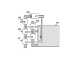
- 13 is a plan view showing an example of a layout of elements in an EVS pixel according to a second embodiment of the present technology.
- FIG. 13 is a plan view showing an example of a layout of elements in an EVS pixel to which a MOS capacitance is added as a coupling capacitance according to a second embodiment of the present technology.
- FIG. 13 is an example of a circuit diagram of an EVS pixel in a case where a logarithmic response unit is switched according to a second embodiment of the present technology.
- 13 is an example of a circuit diagram of an EVS pixel in a case where a sub-pixel is switched according to a second embodiment of the present technology.
- 13 is a block diagram showing a configuration example of a solid-state imaging element according to a first modified example of a second embodiment of the present technology; FIG.
- FIG. 13 is an example of a circuit diagram of an EVS pixel according to a first modified example of the second embodiment of the present technology.
- 13 is an example of a circuit diagram of an EVS pixel according to a second modified example of the second embodiment of the present technology.
- 13 is an example of a circuit diagram of an EVS pixel according to a third modified example of the second embodiment of the present technology.
- FIG. 13 is a block diagram showing a configuration example of a solid-state imaging element according to a third embodiment of the present technology.
- FIG. 13 is a plan view showing an example of a pixel array unit according to a third embodiment of the present technology.
- FIG. 13 is a block diagram showing a configuration example of a solid-state imaging element according to a first modified example of a third embodiment of the present technology.
- FIG. FIG. 13 is a circuit diagram showing a configuration example of a shared block in a first modified example of the third embodiment of the present technology.
- 13 is a block diagram showing a configuration example of a solid-state imaging element according to a second modified example of the third embodiment of the present technology.
- FIG. FIG. 13 is a circuit diagram showing a configuration example of an illuminance meter according to a second modified example of the third embodiment of the present technology.
- 1 is a block diagram showing a schematic configuration example of a vehicle control system;
- FIG. 4 is an explanatory diagram showing an example of an installation position of an imaging unit.
- First embodiment (example of controlling bias voltage according to illuminance) 2.
- Second embodiment (example of controlling capacitance value according to illuminance) 3.
- Third embodiment (an example in which the bias voltage is controlled according to the illuminance and a part of the illuminometer is arranged within the pixel array unit) 4. Examples of applications to moving objects
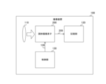
- First embodiment [Configuration example of imaging device] 1 is a block diagram showing an example of a configuration of an imaging device 100 according to a first embodiment of the present technology.
- the imaging device 100 includes an imaging lens 110, a solid-state imaging element 200, a recording unit 120, and a control unit 130.
- Assumed imaging device 100 is a camera mounted on a smartphone, an industrial robot, an in-vehicle camera, or the like.
- the imaging lens 110 focuses the incident light and guides it to the solid-state imaging element 200.
- the solid-state imaging element 200 detects, as an address event, when the amount of change in luminance for each pixel address exceeds a predetermined threshold.
- the solid-state imaging element 200 outputs data indicating the detection result for each pixel to the recording unit 120 via a signal line 209.
- the recording unit 120 records data from the solid-state imaging element 200.
- the control unit 130 controls the solid-state imaging element 200 to detect address events.
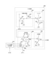
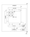
- FIG. 2 is a block diagram showing a configuration example of a solid-state imaging element 200 according to the first embodiment of the present technology.
- the solid-state imaging element 200 includes a readout region selection unit 211, a signal generation unit 212, a pixel array unit 213, a light meter 214, a parameter control circuit 215, and a bias voltage generation circuit 216.
- a pixel array unit 213, a plurality of EVS pixels 300 are arranged in a two-dimensional lattice pattern.
- the EVS pixel 300 detects whether or not the amount of change in luminance exceeds a predetermined threshold (in other words, whether or not an address event has occurred).
- the EVS pixel 300 supplies a detection signal indicating the detection result of the address event to the signal generating unit 212.
- the EVS pixel 300 is an example of a detection pixel as described in the claims.
- the readout region selection unit 211 selects a portion of the multiple EVS pixels 300 included in the pixel array unit 213. For example, the readout region selection unit 211 selects one or more rows among the rows included in the two-dimensional matrix structure corresponding to the pixel array unit 213. The readout region selection unit 211 sequentially selects one or more rows according to a preset period.
- the signal generating unit 212 generates an event signal corresponding to the pixel in which an address event has been detected among the selected pixels based on the output signal of the pixel selected by the readout area selecting unit 211.
- the signal generating unit 212 can be configured to include, for example, a column selection circuit that arbitrates the signals coming into the signal generating unit 212. Furthermore, the signal generating unit 212 can be configured to output not only information about active pixels that detect an address event, but also information about inactive pixels that do not detect an address event.
- the signal generating unit 212 outputs, via the signal line 209, address information and timestamp information (e.g., (X, Y, T)) of the active pixel in which the address event was detected.
- address information and timestamp information e.g., (X, Y, T)
- the data output from the signal generating unit 212 may be not only address information and timestamp information, but also information in a frame format (e.g., (0, 0, 1, 0, ...)).
- the illuminometer 214 measures the illuminance of ambient light. This illuminometer 214 is disposed outside the pixel array section 213.
- the illuminometer 214 is realized by, for example, a photoelectric conversion element, a transistor, or an ADC (Analog to Digital Converter).
- the illuminometer 214 supplies the measured illuminance to the parameter control circuit 215.
- the parameter control circuit 215 controls the parameters of the EVS pixel 300 according to the illuminance measured by the illuminometer 214. For example, the bias voltage among various parameters is controlled.
- the bias voltage generation circuit 216 generates a bias voltage according to the control of the parameter control circuit 215 and supplies it to each of the EVS pixels 300 in the pixel array section 213. Although one bias voltage generation circuit 216 is provided for all pixels, it is also possible to divide the pixel array section 213 into multiple regions and provide a bias voltage generation circuit 216 for each region.
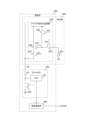
- FIG. 3 is a block diagram showing a configuration example of an EVS pixel according to the first embodiment of the present technology.
- the EVS pixel 300 includes a photoelectric conversion element 310, a logarithmic response unit 320, a buffer 330, a differentiator 340, a comparator 350, and an output circuit 360.
- the bias voltage from the bias voltage generation circuit 216 is supplied to the buffer 330.
- the photoelectric conversion element 310 generates a photocurrent by photoelectric conversion.
- the logarithmic response unit 320 converts the photocurrent of the photoelectric conversion element 310 into a logarithmic voltage and supplies it to the buffer 330.
- Buffer 330 supplies an output signal corresponding to the logarithmic voltage to differentiator 340.
- Differentiator 340 differentiates the output signal of buffer 330 to generate a differentiated signal, which it supplies to comparator 350.
- Comparator 350 compares the differential signal with a predetermined threshold and supplies the comparison result to output circuit 360.
- Output circuit 360 generates a detection signal based on the comparison result and outputs it to signal generation unit 212.
- the address event includes, for example, at least one of an on event indicating that the amount of increase in luminance has exceeded the threshold, and an off event indicating that the amount of decrease in luminance has exceeded the threshold.
- the address event detection signal includes, for example, at least one of one bit indicating the detection result of an on event and one bit indicating the detection result of an off event.
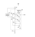
- FIG. 4 is a circuit diagram showing an example configuration of an EVS pixel 300 in the first embodiment of the present technology.
- the logarithmic response unit 320 includes a log transistor 321, a current source transistor 327, and a TIA (TransImpedance Amplifier) 324.
- a log transistor 321, a current source transistor 327, and a TIA (TransImpedance Amplifier) 324 for example, an nMOS (n-channel Metal Oxide Semiconductor) transistor is used as the log transistor 321 and the TIA 324.
- a pMOS (p-channel MOS) transistor is used as the current source transistor 327.
- the log transistor 321 is inserted between the power supply voltage and the photoelectric conversion element 310.
- the current source transistor 327 and the TIA 324 are connected in series between the power supply voltage and a reference voltage (such as a ground voltage).
- connection node between the log transistor 321 and the photoelectric conversion element 310 is connected to the gate of the TIA 324.
- the connection node between the current source transistor 327 and the TIA 324 is connected to the gate of the log transistor 321 and the buffer 330.
- a fixed bias voltage Vblog is applied to the gate of the current source transistor 327.
- the log transistor 321 converts the photocurrent generated by the photoelectric conversion element 310 into a logarithmic voltage.
- the TIA 324 inverts and amplifies the logarithmic voltage. Note that in the figure, the loop circuit consisting of the log transistor 321 and the TIA 324 is one stage, but it can also be two or more stages, as described below.
- the buffer 330 includes a source follower transistor 331 and an nMOS transistor 332.
- an nMOS transistor is used as the source follower transistor.
- the source follower transistor 331 and the nMOS transistor 332 are connected in series between the power supply voltage and the reference voltage.
- the logarithmic voltage Vp from the logarithmic response unit 320 is input to the gate of the source follower transistor 331, and the source of the source follower transistor 331 is connected to the differentiator 340.
- the bias voltage Vbsf generated by the bias voltage generation circuit 216 is input to the gate of the nMOS transistor 332.
- the source follower transistor 331 supplies an output signal corresponding to the logarithmic voltage Vp to the differentiator 340. Furthermore, the nMOS transistor 332 supplies a bias current Ib corresponding to the bias voltage Vbsf.
- the parameter control circuit 215 controls the bias voltage Vbsf according to the illuminance. The details of the control will be described later. Note that the bias voltage Vbsf is an example of the first bias voltage described in the claims.
- Differentiator 340 includes capacitors 341 and 343, pMOS transistor 344, nMOS transistors 342 and 345, and bias switch 346.
- One end of the capacitance 341 is connected to the buffer 330, and the other end is connected to one end of the capacitance 343 and the gate of the pMOS transistor 344.
- a reset signal rst is input to the gate of the nMOS transistor 342, and the source and drain are connected to both ends of the capacitance 343.
- the pMOS transistor 344 and the nMOS transistor 345 are connected in series between the power supply voltage and the reference voltage.
- the other end of the capacitance 343 is connected to the connection point of the pMOS transistor 344 and the nMOS transistor 345.
- a bias voltage from the bias changeover switch 346 is applied to the gate of the nMOS transistor 345 on the reference voltage side, and the connection point of the pMOS transistor 344 and the nMOS transistor 345 is also connected to the comparator 350.
- the nMOS transistor 345 supplies a bias current according to the bias voltage.
- the bias changeover switch 346 selects one of the bias voltages AZ, POS, and NEG according to the selection signal SW from the readout area selection unit 211, and supplies it to the nMOS transistor 345.
- the bias voltage AZ is supplied during auto-zero.
- the bias voltage POS is supplied during the detection period of an on-event, and the bias voltage NEG is supplied during the detection period of an off-event. These bias voltages are assumed to be fixed values.
- the differentiator 340 during the detection period of an on-event, the differentiator 340 generates a differential signal indicating the amount of increase in luminance and outputs it to the comparator 350.
- the differentiator 340 During the detection period of an off-event, the differentiator 340 generates a differential signal indicating the amount of decrease in luminance and outputs it to the comparator 350.
- the differential signal is initialized by the reset signal rst from the readout area selection unit 211.
- Comparator 350 includes a pMOS transistor 351 and an nMOS transistor 352. These pMOS transistor 351 and nMOS transistor 352 are connected in series between the power supply voltage and the reference voltage.
- the differentiated signal from the differentiator 340 is input to the gate of the pMOS transistor 351 on the power supply side.
- a bias voltage Vth the value of which corresponds to a threshold value, is input to the gate of the nMOS transistor 352.
- This bias voltage Vth is assumed to be a fixed value.
- the voltage at the connection point between the pMOS transistor 351 and the nMOS transistor 352 is output to the output circuit 360 as the comparison result.
- the comparator 350 compares the differential signal indicating the amount of increase or decrease in luminance with the value of the bias voltage Vth (i.e., the threshold value), and outputs the comparison result to the output circuit 360.
- the circuits in the solid-state imaging device 200 can also be distributed across multiple semiconductor chips.
- the light receiving chip and the circuit chip are stacked. Then, the photoelectric conversion element 310, the log transistor 321, and the TIA 324 are arranged on the light receiving chip, and the subsequent circuitry from the current source transistor 327 onwards is arranged on the circuit chip.
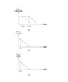
- FIG. 6 is a graph showing an example of frequency characteristics when the bias voltage Vbsf in the first embodiment of the present technology is Vbsf1, which is higher than a predetermined value.
- a shows the frequency characteristics of the logarithmic response unit 320
- b shows the frequency characteristics of the buffer 330
- c shows the frequency characteristics of the entire circuit including the logarithmic response unit 320 and the buffer 330.
- the vertical axis shows the gain
- the horizontal axis shows the frequency.
- the gain is constant in the frequency band below the cutoff frequency, and the gain decreases according to the frequency in the frequency band above the cutoff frequency.
- the cutoff frequency becomes higher as the illuminance increases, and the cutoff frequency when the illuminance is relatively high is denoted by f c_logH , and the cutoff frequency when the illuminance is relatively low is denoted by f c_logL .
- the gain is constant in the frequency band below the cutoff frequency f c_SF1 , and the gain decreases according to the frequency in the frequency band above the cutoff frequency f c_SF1 .
- This cutoff frequency f c_SF1 is constant regardless of the illuminance.
- Vbsf1 is set to a value that makes the cutoff frequency f c_SF1 higher than f c_logH .
- the frequency characteristics of the logarithmic response section 320 with the lower cutoff frequency in other words the narrower frequency band through which signals pass, dominate the entire circuit.
- FIG. 7 is a graph showing an example of frequency characteristics when the bias voltage Vbsf in the first embodiment of the present technology is Vbsf2, which is lower than a predetermined value.
- a shows the frequency characteristics of the logarithmic response unit 320
- b shows the frequency characteristics of the buffer 330
- c shows the frequency characteristics of the entire circuit including the logarithmic response unit 320 and the buffer 330.
- the vertical axis in a, b, and c shows the gain
- the horizontal axis shows the frequency.
- the cutoff frequency of the logarithmic response unit 320 changes depending on the illuminance.
- the cutoff frequency f c_SF2 of the buffer 330 is constant regardless of the illuminance.
- Vbsf2 is set to a value that makes the cutoff frequency f c_SF2 lower than f c_logL .
- the frequency characteristics of the buffer 330 with the narrower frequency band dominate the entire circuit.
- the frequency band can be narrowed by controlling the bias voltage Vbsf to the lower Vbsf2.
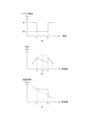
- FIG. 8 is a graph showing an example of bias current, noise, and delay time according to illuminance in the first embodiment of the present technology.
- a is a graph showing an example of the relationship between illuminance and bias current in the buffer 330.
- the vertical axis represents bias current
- the horizontal axis represents illuminance.
- b is a graph showing an example of the relationship between noise generated in a dark state and illuminance.
- the vertical axis of the figure, b indicates the noise BGR (Background Rate), and the horizontal axis indicates the frequency.
- the dashed dotted line indicates the BGR when the bias voltage Vbsf to the buffer 330 is fixed, and the solid line indicates the BGR when the bias voltage Vbsf is controlled so as to generate the bias current of the figure, a.
- C in the figure is a graph showing an example of the relationship between illuminance and the delay time of the EVS pixel 300.
- the vertical axis of c in the figure shows the delay time, and the horizontal axis shows the frequency.
- the dashed dotted line shows the delay time when the bias voltage Vbsf to the buffer 330 is fixed, and the solid line shows the delay time when the bias voltage Vbsf is controlled to generate the bias current of a in the figure.
- the parameter control circuit 215 when the illuminance is within the range of L 1 L to L 1 H , the parameter control circuit 215 generates the bias voltage Vbsf2 and reduces the bias current to Ib2, which is lower than the predetermined value. On the other hand, when the illuminance is outside the range of L 1 L to L 1 H , the parameter control circuit 215 generates the bias voltage Vbsf1 and increases the bias current to Ib1, which is higher than the predetermined value. As described above, by controlling the bias voltage Vbsf to the lower Vbsf2, the frequency band through which the signal passes can be narrowed.
- the parameter control circuit 215 lowering the bias voltage within the range of L 1 L to L 1 H , the noise peak can be suppressed compared to the case where the bias voltage is set to a fixed value. Furthermore, since the peak can be sufficiently suppressed, the frequency band of the logarithmic response unit 320 can also be slightly narrowed. By narrowing the frequency band, the delay time at an illuminance lower than L 1 L can be reduced.
- FIG. 9 is a diagram showing an example of readout control of the EVS pixel 300 in the first embodiment of the present technology.
- the readout region selection unit 211 selects rows in the pixel array unit 213 one by one in sequence, and causes each of the EVS pixels 300 in the row to detect an address event. Note that the readout region selection unit 211 can also select n rows (n is an integer equal to or greater than 2) in sequence.
- the read area selection unit 211 supplies a reset signal rst to that row and switches the bias voltage in the differentiator 340 to AZ.
- the readout area selection unit 211 switches the bias voltage in the differentiator 340 to POS.
- the readout area selection unit 211 switches the bias voltage in the differentiator 340 to NEG.
- the method of reading out row by row in sequence is called the scan method.
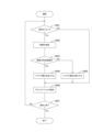
- FIG. 10 is a flowchart showing an example of the operation of the solid-state imaging device 200 in the first embodiment of the present technology. This operation is started, for example, when a specific application for detecting an address event is executed.
- the illuminance meter 214 judges whether the current time is the timing for measuring the illuminance (step S901). The illuminance is measured, for example, at regular intervals. If it is the timing for measuring the illuminance (step S901: Yes), the illuminance meter 214 measures the illuminance (step S902). The parameter control circuit 215 judges whether the measured illuminance is within a predetermined range from L L to L H (step S903). If the illuminance is within the predetermined range (step S903: Yes), the parameter control circuit 215 makes the bias voltage lower than a predetermined value (step S904). On the other hand, if the illuminance is outside the predetermined range (step S903: No), the parameter control circuit 215 makes the bias voltage higher than a predetermined value (step S905).
- step S901 If it is not time to measure the illuminance (step S901: No), or after step S904 or S905, the readout area selection unit 211 detects address events on a row-by-row basis (step S906). After step S906, the readout area selection unit 211 determines whether to end the readout (step S906).
- step S907: No If the readout is not to be ended (step S907: No), the readout area selection unit 211 returns to step S901. On the other hand, if the readout is to be ended (step S907: No), the solid-state imaging element 200 ends the operation for detecting an address event.
- the parameter control circuit 215 controls the bias voltage Vbsf to the buffer 330 according to the illuminance, thereby suppressing noise.
- the parameter control circuit 215 controls the bias voltage Vbsf to the buffer 330, but is not limited to this configuration.
- the parameter control circuit 215 in the first modification of the first embodiment differs from the first embodiment in that it controls the bias voltage to the differentiator 340.
- FIG. 11 is a circuit diagram showing an example of the configuration of an EVS pixel 300 in a first modified example of the first embodiment of the present technology.
- a fixed bias voltage Vbsf is applied to the buffer 330.
- the bias voltage generation circuit 216 generates bias voltages AZ, POS, and NEG for the differentiator 340.
- the parameter control circuit 215 controls the bias voltages POS and NEG according to the illuminance.
- a fixed value is set for the bias voltage AZ.
- the bias voltages POS and NEG are an example of a second bias voltage described in the claims.
- FIG. 12 is a diagram showing an example of bias current, noise, and delay according to illuminance in a first modified example of the first embodiment of the present technology.
- a is a graph showing an example of the relationship between the positive bias current and illuminance according to the bias voltage POS.
- a is a graph showing an example of the relationship between the negative bias current and illuminance according to the bias voltage NEG.
- the vertical axis indicates the bias current
- the horizontal axis indicates the illuminance.
- C in the figure is a graph showing an example of the relationship between noise generated in a dark state and illuminance.
- the vertical axis of c in the figure shows the noise BGR, and the horizontal axis shows the frequency.
- the dashed dotted line shows the BGR when the bias voltages POS and NEG are fixed, and the solid line shows the BGR when the bias voltages POS or NEG are controlled to generate the bias current of a or b in the figure.
- d is a graph showing an example of the relationship between illuminance and the delay time of the EVS pixel 300.
- the vertical axis of d in the figure shows the delay time, and the horizontal axis shows the frequency.
- the dashed dotted line shows the delay time when the bias voltages POS and NEG are fixed, and the solid line shows the delay time when the bias voltage POS or NEG is controlled to generate the bias current of a or b in the figure.
- the parameter control circuit 215 when the illuminance is within the range of L L to L H , the parameter control circuit 215 generates a bias voltage POS2 and reduces the positive bias current to Ip2, which is lower than the predetermined value.
- the parameter control circuit 215 when the illuminance is outside the range of L L to L H , the parameter control circuit 215 generates a bias voltage POS1, which is higher than POS2, and increases the positive bias current to Ip1, which is higher than the predetermined value.
- the parameter control circuit 215 during the detection period of an off event, when the illuminance is within the range of L L to L H , the parameter control circuit 215 generates a bias voltage NEG1 and increases the negative bias current to In1, which is higher than a predetermined value. On the other hand, when the illuminance is outside the range of L L to L H , the parameter control circuit 215 generates a bias voltage NEG2, which is lower than NEG1, and decreases the bias current to In2, which is lower than the predetermined value.
- the delay time becomes longer within the range from L 1 L to L 1 H than when the bias voltage is a fixed value.
- the parameter control circuit 215 can also control the bias voltage Vbsf to the buffer 330 in accordance with the illuminance, in addition to the bias voltages POS and NEG.
- the EVS pixel 300 detects both on-events and off-events, but can also detect only one of them. In this case, the parameter control circuit 215 controls only one of the bias voltages POS and NEG.
- the bias voltages POS and NEG to the differentiator 340 are controlled according to the illuminance, thereby suppressing noise.
- the parameter control circuit 215 controls the bias voltage Vbsf to the buffer 330, but is not limited to this configuration.
- the parameter control circuit 215 in the second modified example of the first embodiment differs from the first embodiment in that it controls the bias voltage to the comparator 350.
- FIG. 13 is a circuit diagram showing an example of the configuration of an EVS pixel 300 in a second modified example of the first embodiment of the present technology.
- a fixed bias voltage Vbsf is applied to the buffer 330.
- the bias voltage generation circuit 216 generates a bias voltage Vth to the comparator 350.
- the parameter control circuit 215 controls the value (threshold) of the bias voltage Vth according to the illuminance.
- the bias voltage Vth is an example of a third bias voltage described in the claims.
- the method for controlling the bias voltage Vth is the same as the method for controlling the bias voltage Vbsf in the first embodiment.
- the parameter control circuit 215 can control the bias voltage Vth to the comparator 350 as well as the bias voltage of at least one of the buffer 330 and the differentiator 340 according to the illuminance.
- the bias voltage Vth to the comparator 350 is controlled according to the illuminance, thereby suppressing noise.
- the parameter control circuit 215 controls the bias voltage Vbsf to the buffer 330, but it is also possible to control parameters other than the bias voltage.
- the parameter control circuit 215 in this second embodiment differs from the first embodiment in that it controls the capacitance value of the logarithmic response unit 320.
- FIG. 14 is a block diagram showing an example of the configuration of a solid-state imaging element 200 in a second embodiment of the present technology.
- the solid-state imaging element 200 in this second embodiment does not include a bias voltage generation circuit 216.
- the parameter control circuit 215 controls the capacitance value of a variable capacitance (not shown) in the EVS pixel 300 according to the illuminance.
- FIG. 15 is a circuit diagram showing an example of a configuration of a logarithmic response unit 320 in the second embodiment of the present technology.
- a is an example of a logarithmic response unit 320 with a single loop circuit.
- b is an example of a logarithmic response unit 320 with a two-stage loop circuit.
- c is an example of a logarithmic response unit 320 with a three-stage loop circuit.
- the logarithmic response unit 320 in the second embodiment differs from the first embodiment in that it further includes a coupling capacitance 328 and a switch 329.
- the coupling capacitance 328 is inserted between the connection point (in other words, the output node) of the current source transistor 327 and the TIA 324 and the switch 329.
- a fixed bias voltage Vbsf is applied to the downstream buffer 330 (not shown).
- the switch 329 opens and closes the path between the connection point (in other words, the input node) of the log transistor 321 and the photoelectric conversion element 310 and the coupling capacitance 328 under the control of the parameter control circuit 215.
- the parameter control circuit 215 turns the switch 329 on and off depending on the illuminance. For example, when the illuminance is low and below a threshold, the parameter control circuit 215 controls the switch 329 to the off state, and when the illuminance is high and above the threshold, the parameter control circuit 215 turns the switch 329 on and inserts the coupling capacitance 328.
- the loop circuit consisting of the log transistor 321 and the TIA 324 is one stage, but the loop circuit is not limited to one stage.
- log transistor 322 and TIA 325 can be added to form a two-stage loop circuit.
- log transistor 322 is inserted between log transistor 321 and the input node
- TIA 325 is inserted between TIA 324 and a reference voltage (such as a ground voltage).
- the gate of log transistor 322 is connected to the connection point between TIAs 324 and 325, and the gate of TIA 325 is connected to the input node.
- a log transistor 323 and a TIA 326 can be further added to make the loop circuit three stages.
- log transistor 323 is inserted between log transistor 322 and the input node
- TIA 326 is inserted between TIA 325 and the reference voltage.
- the gate of log transistor 323 is connected to the connection point of TIA 325 and 326, and the gate of TIA 326 is connected to the input node.
- the loop circuit can also be four or more stages.
- diode-connected nMOS transistors can be inserted.
- a diode-connected nMOS transistor 322-1 is added between the log transistor 321 and the input node.
- a diode-connected nMOS transistor 323-1 is further added between the nMOS transistor 322-1 and the input node.
- Diode-connected nMOS transistors can also be provided in three or more stages.
- FIG. 17 is a circuit diagram showing an example of the configuration of a logarithmic response unit to which coupling capacitances and switches have been added in the second embodiment of the present technology.
- coupling capacitances 328-1 and 328-2 and switches 329-1 and 329-2 have been added.
- One end of coupling capacitances 328-1 and 328-2 is commonly connected to the output node.
- Switch 329-1 opens and closes the path between the other end of coupling capacitance 328-1 and the input node
- switch 329-2 opens and closes the path between the other end of coupling capacitance 328-2 and the input node.
- the parameter control circuit 215 can open and close each of the multiple switches individually. By controlling these switches, the number of coupling capacitances connected in parallel between the input node and the output node increases or decreases, and the combined capacitance of these changes.
- the coupling capacitance is an example of a variable capacitance as described in the claims.
- the circuit configuration of the logarithmic response unit 320 is not limited to those illustrated in Figures 15 to 17.
- M (M is an integer) switches such as switch 329-1 and M coupling capacitances such as coupling capacitance 328-1 can be inserted between the output node and the reference voltage.
- FIG. 19 is a diagram showing an example of the number of capacitors, noise, and delay according to illuminance in a first modified example of the second embodiment of the present technology.
- a is a graph showing an example of the relationship between the number of capacitors connected in parallel and illuminance.
- the vertical axis of a in the figure shows the number of capacitors, and the horizontal axis shows the illuminance.
- b is a graph showing an example of the relationship between noise occurring in a dark state and illuminance.
- the vertical axis of b in the same figure shows the noise BGR, and the horizontal axis shows the frequency.
- the dashed dotted line shows the BGR when the number of capacitances of the logarithmic response unit 320 is fixed, and the solid line shows the BGR when the number of capacitances is controlled as exemplified in a in the same figure.
- C in the figure is a graph showing an example of the relationship between illuminance and the delay time of the EVS pixel 300.
- the vertical axis of c in the figure shows the delay time, and the horizontal axis shows the frequency.
- the dashed dotted line shows the delay time when the number of capacitances of the logarithmic response unit 320 is fixed, and the solid line shows the delay time when the number of capacitances is controlled as exemplified in a in the figure.
- the parameter control circuit 215 sets the number of capacitors to m1, which is greater than the predetermined value, and increases the capacitance value of the composite capacitor.
- the parameter control circuit 215 sets the number of capacitors to m2, which is less than the predetermined value, and decreases the capacitance value of the composite capacitor. This control makes it possible to suppress noise peaks compared to when the number of capacitors is a fixed value, as shown in FIG. 1B.
- the delay time becomes longer within the range from L L to L H than when the capacitance value is fixed.
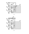
- FIG. 20(a) shows a layout of photoelectric conversion element 310, log transistors 321 and 322, TIAs 324 and 325, switch 329, and coupling capacitance 328.
- Figure 20(b) diffusion capacitance can be added as coupling capacitance 328.
- a MOS capacitance can be added as coupling capacitance 328.
- the coupling capacitance in the logarithmic response unit 320 is variable, but this configuration is not limited to this.
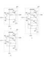
- logarithmic response units 320-1 and 320-2 with different coupling capacitances can be arranged in the EVS pixel 300, and the connection destination of their input nodes can be switched by switches 329-1 and 329-2.
- switch 329-1 opens and closes the path between the input node of logarithmic response unit 320-1 and the photoelectric conversion element 310
- switch 329-2 opens and closes the path between the input node of logarithmic response unit 320-2 and the photoelectric conversion element 310.
- the output nodes of logarithmic response units 320-1 and 320-2 are commonly connected to the subsequent buffer 330.
- the parameter control circuit 215 selects one of logarithmic response units 320-1 and 320-2 according to the illuminance, and controls switches 329-1 and 329-2 to connect it to the photoelectric conversion element 310.
- photoelectric conversion element 310-1 is connected to the input node of logarithmic response unit 320-1
- photoelectric conversion element 310-2 is connected to the input node of logarithmic response unit 320-2
- Switch 329-1 opens and closes the path between the output node of logarithmic response unit 320-1 and buffer 330
- switch 329-2 opens and closes the path between the output node of logarithmic response unit 320-2 and buffer 330.
- Parameter control circuit 215 selects one of logarithmic response units 320-1 and 320-2 depending on the illuminance, and controls switches 329-1 and 329-2 to connect to buffer 330.
- the circuit including the photoelectric conversion element 310-1 and the logarithmic response unit 320-1 functions as one of a pair of subpixels in the EVS pixel 300, and the circuit including the photoelectric conversion element 310-2 and the logarithmic response unit 320-2 functions as the other of the pair of subpixels.
- the parameter control circuit 215 switches the connection destination of two logarithmic response units, but it is also possible to provide three or more logarithmic response units with different coupling capacitances and switch between them.
- the parameter control circuit 215 can also control the bias voltage to at least one of the buffer 330, the differentiator 340, and the comparator 350.
- the parameter control circuit 215 controls the capacitance value of the variable capacitance in the EVS pixel 300 according to the illuminance, thereby suppressing noise.
- the parameter control circuit 215 controls the capacitance value of the variable capacitance in the EVS pixel 300, but is not limited to this configuration.
- the solid-state imaging device 200 in the first modified example of the second embodiment differs from the second embodiment in that it reads out at least one of a plurality of EVS pixels having different coupling capacitances.
- the solid-state imaging element 200 in the first modified example of the second embodiment includes a readout region selection unit 211, a signal generation unit 212, a pixel array unit 213, and a light meter 214.
- a predetermined number of EVS pixels 300-1 and a predetermined number of EVS pixels 300-2 are arranged in a two-dimensional lattice shape in the pixel array unit 213.
- the coupling capacitance C pr1 in the EVS pixel 300-1 is a different value from the coupling capacitance C pr2 in the EVS pixel 300-2.
- the EVS pixels 300-1 and 300-2 are examples of the first and second pixels described in the claims.
- the illuminance meter 214 supplies the measured illuminance to the readout area selection unit 211.
- the readout area selection unit 211 selects and reads out one of the EVS pixels 300-1 and 300-2 depending on the illuminance. For example, when the illuminance is lower than a threshold value, the readout area selection unit 211 selects the EVS pixel 300-1 or 300-2 with the smaller coupling capacitance, and when the illuminance is equal to or higher than the threshold value, the readout area selection unit 211 selects the EVS pixel 300-1 or 300-2 with the larger coupling capacitance. This makes it possible to suppress noise in the same way as in the second embodiment.
- the readout area selection unit 211 can read out all the EVS pixels. In this case, processing according to various illuminance levels can be performed in a downstream circuit.
- FIG. 25 is an example of a circuit diagram of an EVS pixel 300-1 in a first modified example of the second embodiment of the present technology.
- This EVS pixel 300-1 includes a photoelectric conversion element 310, a logarithmic response unit 320, a buffer 330, a differentiator 340, and a comparator 350.
- the coupling capacitance of the logarithmic response unit 320 is a fixed value.
- the bias voltage is a fixed value.
- the circuit configuration of the EVS pixel 300-2 is the same as that of the EVS pixel 300-1, except that the coupling capacitance is different.
- the readout area selection unit 211 selects one of the EVS pixels 300-1 and 300-2, which have different coupling capacitances depending on the illuminance, thereby suppressing noise.
- the parameter control circuit 215 controls the capacitance value of the variable capacitance in the EVS pixel 300 in response to the illuminance, but the capacitance value can also be controlled in response to a measured value other than the illuminance.
- the solid-state imaging element 200 in the second modified example of the second embodiment differs from the second embodiment in that it measures a voltage instead of the illuminance and controls the capacitance value of the variable capacitance in response to the voltage value.
- FIG. 26 is an example of a circuit diagram of an EVS pixel 300 in a second modified example of the second embodiment of the present technology.
- the illuminometer 214 is not arranged in the solid-state imaging element 200.
- a voltmeter 371 and a parameter control circuit 215 are further arranged in the pixel 300.
- the circuit configuration of the logarithmic response unit 320 in the second modified example of the second embodiment is the same as in the second embodiment.
- the voltmeter 371 measures the voltage at the output node of the logarithmic response unit 320 and supplies the measured value to the parameter control circuit 215.
- the voltmeter 371 is an example of a measurement unit described in the claims.
- the parameter control circuit 215 controls the capacitance value of the variable capacitance in the logarithmic response unit 320 according to the voltage value. For example, when the voltage value is lower than a threshold value, the parameter control circuit 215 controls the switch 329 to the off state, and when the voltage value is equal to or higher than the threshold value, the parameter control circuit 215 controls the switch 329 to the on state, inserting the coupling capacitance 328. This suppresses noise.
- the parameter control circuit 215 controls the variable capacitance for each EVS pixel 300 according to its voltage value, but is not limited to this control.
- the parameter control circuit 215 can obtain statistics (average or sum) of the voltage values of all pixels, and control the variable capacitance of each of all pixels according to the statistics.
- the parameter control circuit 215 can obtain statistics (average or sum) of the voltage values of the EVS pixels 300 in each area, and control the variable capacitance in the area according to the statistics.
- the parameter control circuit 215 controls the capacitance value of the variable capacitance in the EVS pixel 300 according to the voltage value, thereby suppressing noise.
- the parameter control circuit 215 controls the capacitance value of the variable capacitance in the EVS pixel 300 in response to the illuminance, but the capacitance value can also be controlled in response to a measured value other than the illuminance.
- the solid-state imaging device 200 in the third modified example of the second embodiment differs from the second embodiment in that it measures a current instead of the illuminance and controls the capacitance value of the variable capacitance in response to the current value.
- FIG. 27 is an example of a circuit diagram of an EVS pixel 300 in a third modified example of the second embodiment of the present technology.
- the illuminometer 214 is not arranged in the solid-state imaging element 200.
- an ammeter 372 and a parameter control circuit 215 are further arranged in the pixel 300.
- the circuit configuration of the logarithmic response unit 320 in the third modified example of the second embodiment is the same as in the second embodiment.
- the ammeter 372 measures the current flowing through the logarithmic response unit 320 and supplies the measured value to the parameter control circuit 215.
- the ammeter 372 is an example of a measurement unit described in the claims.
- the parameter control circuit 215 controls the capacitance value of the variable capacitance in the logarithmic response unit 320 according to the current value. For example, when the current value is smaller than a threshold value, the parameter control circuit 215 controls the switch 329 to the off state, and when the current value is equal to or greater than the threshold value, the parameter control circuit 215 controls the switch 329 to the on state, inserting the coupling capacitance 328. This suppresses noise.
- the parameter control circuit 215 controls the variable capacitance for each EVS pixel 300 according to its current value, but is not limited to this control.
- the parameter control circuit 215 can obtain statistics (average or total) of the current values of all pixels, and control the variable capacitance of each of all pixels according to the statistics.
- the parameter control circuit 215 can obtain statistics (average or total) of the current values of the EVS pixels 300 in each area, and control the variable capacitance within the area according to the statistics.
- the parameter control circuit 215 controls the capacitance value of the variable capacitance in the EVS pixel 300 according to the current value, thereby suppressing noise.
- the illuminometer 214 is arranged outside the pixel array section 213, but this is not limited to the configuration.
- the solid-state imaging device 200 in the third embodiment differs from the first embodiment in that a part of the illuminometer is arranged inside the pixel array section 213.
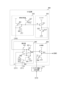
- FIG. 28 is a block diagram showing an example of the configuration of a solid-state imaging device 200 in a third embodiment of the present technology.
- the solid-state imaging device 200 in this third embodiment differs from the first embodiment in that it further includes a driving unit 217, and includes a predetermined number of light receiving units 220, a column ADC 230, and an illuminance calculation unit 240 instead of the illuminometer 214.
- a predetermined number of light receiving sections 220 are arranged in the pixel array section 213. Each of these light receiving sections 220 can be used as a gradation pixel that generates a gradation signal. For example, two of the four pixels in two rows and two columns in the pixel array section 213 are replaced with light receiving sections 220 (in other words, gradation pixels).
- the ratio of the number of pixels and the area of the gradation pixels to the EVS pixels 300 is not limited to 1:1.
- the number of pixels of the gradation pixels can be made greater than the EVS pixels 300, and the area of the gradation pixels can be made smaller than that of the EVS pixels 300.
- the driving unit 217 drives each of the light receiving units 220.
- the light receiving units 220 generate analog signals corresponding to the luminance and supply them to the column ADC 230.
- the column ADC 230 converts the analog signals for each column into digital signals and supplies them to the illuminance calculation unit 240.
- the illuminance calculation unit 240 calculates the illuminance from the digital signal and supplies it to the parameter control circuit 215.
- the column ADC 230 can also output data that is an array of digital signals as image data.
- FIG. 29 is a circuit diagram showing an example configuration of the light receiving unit 220 and the column ADC 230 in the third embodiment of the present technology.
- the light receiving unit 220 includes a photoelectric conversion element 221 and an analog signal generation circuit 222.
- the analog signal generation circuit 222 includes a transfer transistor 223, a reset transistor 224, a floating diffusion layer 225, an amplification transistor 226, and a selection transistor 227.
- the photoelectric conversion element 221 generates electric charges by photoelectric conversion.
- the photoelectric conversion element 310 in the EVS pixel 300 is an example of a first photoelectric conversion element described in the claims
- the photoelectric conversion element 221 is an example of a second photoelectric conversion element described in the claims.
- the transfer transistor 223 transfers charge from the photoelectric conversion element 221 to the floating diffusion layer 225 in accordance with a transfer signal TRG from the drive unit 217.
- the reset transistor 224 initializes the floating diffusion layer 225 in accordance with a reset signal RST from the drive unit 217.
- the amplification transistor 226 amplifies the voltage of the floating diffusion layer 225 to generate an analog signal.
- the selection transistor 227 supplies an analog signal to a vertical signal line VSL in accordance with a selection signal SEL from the drive unit 217.
- the vertical signal line VSL is wired for each column of the light receiving unit 220.
- the column ADC 230 includes an ADC 231 and a load MOS transistor 232 for each column of the light receiving section 220.
- the ADC 231 converts an analog signal from the corresponding vertical signal line VSL into a digital signal and supplies it to the illuminance calculation section 240.
- a single-slope type ADC is used as the ADC 231.
- the load MOS transistor 232 supplies a constant current.
- the illuminance calculation unit 240 calculates the statistics (average or sum) of the digital signal values from the light receiving unit 220 within the photometric range, and supplies this value to the parameter control circuit 215 as illuminance.
- the circuit including all of the analog signal generating circuits 222, the column ADC 230, and the illuminance calculation unit 240 functions as an illuminance meter 250.
- the illuminance of the pixel array section 213 can be measured more accurately than in the first embodiment in which the illuminometer 214 is arranged outside the pixel array section 213.
- the EVS pixels 300 can be arranged at a constant interval in the pixel array section 213.
- the EVS pixel is arranged at the bottom right, and the light receiving section 220 is arranged in the remaining space.
- first and second variations of the first embodiment and the second embodiment can be applied to the third embodiment.
- a part of the illuminometer 250 is disposed in the pixel array section 213, so that the illuminance of the pixel array section 213 can be accurately measured.
- a photoelectric conversion element is disposed in each of the light receiving section 220 and the EVS pixel 300, but this configuration may result in an insufficient light receiving area for each pixel.
- the solid-state imaging device 200 in the first modified example of the third embodiment differs from the first embodiment in that the light receiving section 220 and the EVS pixel 300 share one photoelectric conversion element.
- FIG. 31 is a block diagram showing an example of the configuration of a solid-state imaging element 200 in a first modified example of the third embodiment of the present technology.
- the solid-state imaging element 200 in the first modified example of the third embodiment differs from the third embodiment in that a predetermined number of shared blocks 400 are arranged in the pixel array section 213.
- FIG. 32 is a circuit diagram showing an example configuration of a shared block 400 in a first modified example of the third embodiment of the present technology.
- the shared block 400 includes a light receiving unit 220, an OFG transistor 305, a logarithmic response unit 320, a buffer 330, a differentiator 340, a comparator 350, and an output circuit 360.
- the buffer 330, the differentiator 340, the comparator 350, and the output circuit 360 are omitted.
- the OFG transistor 305 opens and closes the path between the photoelectric conversion element 221 in the light receiving unit 220 and the logarithmic response unit 320 according to a control signal OFG from the readout area selection unit 211.
- the circuit consisting of the photoelectric conversion element 221, the OFG transistor 305, the logarithmic response unit 320, the buffer 330, the differentiator 340, the comparator 350, and the output circuit 360 functions as the EVS pixel 300.
- the light receiving unit 220 and the EVS pixel 300 share one photoelectric conversion element 221.
- the transfer transistor 223 When measuring illuminance or generating a gradation signal, the transfer transistor 223 is controlled to the on state, and the OFG transistor 305 is controlled to the off state.
- the transfer transistor 223 when detecting an address event, the transfer transistor 223 is controlled to the off state, and the OFG transistor 305 is controlled to the on state.
- the light receiving section 220 and the EVS pixel 300 share the photoelectric conversion element 221, which makes it possible to increase the light receiving area per pixel compared to a case in which a photoelectric conversion element is disposed in each of the light receiving section 220 and the EVS pixel 300.
- first and second variations of the first embodiment and the second embodiment can be applied to the first variation of the third embodiment.
- the light receiving section 220 and the EVS pixel 300 share one photoelectric conversion element 221, so the light receiving area per pixel can be made larger than in the third embodiment.
- the light receiving unit 220 is disposed in the pixel array unit 213, but the present invention is not limited to this configuration.
- the solid-state imaging device 200 in the second modified example of the third embodiment differs from the third embodiment in that the circuit scale of the illuminometer 250 is reduced.
- FIG. 33 is a block diagram showing an example of the configuration of a solid-state imaging element 200 in a second modified example of the third embodiment of the present technology.
- the solid-state imaging element 200 in the second modified example of the third embodiment differs from the third embodiment in that only EVS pixels 300 are arranged in the pixel array section 213.
- FIG. 34 is a circuit diagram showing an example configuration of an illuminometer 250 in a second modified example of the third embodiment of the present technology.
- R is an integer
- R analog signal generation circuits 222 are arranged for each column in the pixel array section 213.
- Each analog signal generation circuit 222 includes a changeover switch 228.
- the rth changeover switch 228 (r is an integer from 1 to R) is arranged in the rth row.
- the changeover switch 228 connects the power supply node of the logarithmic response unit 320 in the corresponding EVS pixel 300 to the vertical signal line VSL according to the control of the readout area selection unit 211.
- the changeover switch 228 is controlled to the ON state during the period in which the illuminance is measured, and the changeover switch 228 is controlled to the OFF state during the period in which an address event is detected.
- first and second variations of the first embodiment and the second embodiment can be applied to the second variation of the third embodiment.
- the technology according to the present disclosure can be applied to various products.
- the technology according to the present disclosure may be realized as a device mounted on any type of moving body such as an automobile, an electric vehicle, a hybrid electric vehicle, a motorcycle, a bicycle, a personal mobility device, an airplane, a drone, a ship, or a robot.
- FIG. 35 is a block diagram showing a schematic configuration example of a vehicle control system, which is an example of a mobile object control system to which the technology disclosed herein can be applied.
- the vehicle control system 12000 includes a plurality of electronic control units connected via a communication network 12001.
- the vehicle control system 12000 includes a drive system control unit 12010, a body system control unit 12020, an outside vehicle information detection unit 12030, an inside vehicle information detection unit 12040, and an integrated control unit 12050.
- Also shown as functional components of the integrated control unit 12050 are a microcomputer 12051, an audio/video output unit 12052, and an in-vehicle network I/F (interface) 12053.
- the drive system control unit 12010 controls the operation of devices related to the drive system of the vehicle according to various programs.
- the drive system control unit 12010 functions as a control device for a drive force generating device for generating the drive force of the vehicle, such as an internal combustion engine or a drive motor, a drive force transmission mechanism for transmitting the drive force to the wheels, a steering mechanism for adjusting the steering angle of the vehicle, and a braking device for generating a braking force for the vehicle.
- the body system control unit 12020 controls the operation of various devices installed in the vehicle body according to various programs.
- the body system control unit 12020 functions as a control device for a keyless entry system, a smart key system, a power window device, or various lamps such as headlamps, tail lamps, brake lamps, turn signals, and fog lamps.
- radio waves or signals from various switches transmitted from a portable device that replaces a key can be input to the body system control unit 12020.
- the body system control unit 12020 accepts the input of these radio waves or signals and controls the vehicle's door lock device, power window device, lamps, etc.
- the outside-vehicle information detection unit 12030 detects information outside the vehicle equipped with the vehicle control system 12000.
- the image capturing unit 12031 is connected to the outside-vehicle information detection unit 12030.
- the outside-vehicle information detection unit 12030 causes the image capturing unit 12031 to capture images outside the vehicle and receives the captured images.
- the outside-vehicle information detection unit 12030 may perform object detection processing or distance detection processing for people, cars, obstacles, signs, characters on the road surface, etc. based on the received images.
- the imaging unit 12031 is an optical sensor that receives light and outputs an electrical signal according to the amount of light received.
- the imaging unit 12031 can output the electrical signal as an image, or as distance measurement information.
- the light received by the imaging unit 12031 may be visible light, or may be invisible light such as infrared light.
- the in-vehicle information detection unit 12040 detects information inside the vehicle.
- a driver state detection unit 12041 that detects the state of the driver is connected.
- the driver state detection unit 12041 includes, for example, a camera that captures an image of the driver, and the in-vehicle information detection unit 12040 may calculate the driver's degree of fatigue or concentration based on the detection information input from the driver state detection unit 12041, or may determine whether the driver is dozing off.
- the microcomputer 12051 can calculate control target values for the driving force generating device, steering mechanism, or braking device based on information inside and outside the vehicle acquired by the outside-vehicle information detection unit 12030 or the inside-vehicle information detection unit 12040, and output control commands to the drive system control unit 12010.
- the microcomputer 12051 can perform cooperative control aimed at realizing the functions of an Advanced Driver Assistance System (ADAS), including vehicle collision avoidance or impact mitigation, following driving based on the distance between vehicles, maintaining vehicle speed, vehicle collision warning, or vehicle lane departure warning.
- ADAS Advanced Driver Assistance System
- the microcomputer 12051 can also perform cooperative control for the purpose of autonomous driving, which allows the vehicle to travel autonomously without relying on the driver's operation, by controlling the driving force generating device, steering mechanism, braking device, etc. based on information about the surroundings of the vehicle acquired by the outside vehicle information detection unit 12030 or the inside vehicle information detection unit 12040.
- the microcomputer 12051 can also output control commands to the body system control unit 12020 based on information outside the vehicle acquired by the outside information detection unit 12030. For example, the microcomputer 12051 can control the headlamps according to the position of a preceding vehicle or an oncoming vehicle detected by the outside information detection unit 12030, and perform cooperative control aimed at preventing glare, such as switching from high beams to low beams.
- the audio/image output unit 12052 transmits at least one output signal of audio and image to an output device capable of visually or audibly notifying the occupants of the vehicle or the outside of the vehicle of information.
- an audio speaker 12061, a display unit 12062, and an instrument panel 12063 are exemplified as output devices.
- the display unit 12062 may include, for example, at least one of an on-board display and a head-up display.
- FIG. 36 shows an example of the installation position of the imaging unit 12031.
- the imaging unit 12031 includes imaging units 12101, 12102, 12103, 12104, and 12105.
- the imaging units 12101, 12102, 12103, 12104, and 12105 are provided, for example, at the front nose, side mirrors, rear bumper, back door, and upper part of the windshield inside the vehicle cabin of the vehicle 12100.
- the imaging unit 12101 provided at the front nose and the imaging unit 12105 provided at the upper part of the windshield inside the vehicle cabin mainly acquire images of the front of the vehicle 12100.
- the imaging units 12102 and 12103 provided at the side mirrors mainly acquire images of the sides of the vehicle 12100.
- the imaging unit 12104 provided at the rear bumper or back door mainly acquires images of the rear of the vehicle 12100.
- the imaging unit 12105 provided at the upper part of the windshield inside the vehicle cabin is mainly used to detect leading vehicles, pedestrians, obstacles, traffic lights, traffic signs, lanes, etc.
- FIG. 36 shows an example of the imaging ranges of the imaging units 12101 to 12104.
- Imaging range 12111 indicates the imaging range of the imaging unit 12101 provided on the front nose
- imaging ranges 12112 and 12113 indicate the imaging ranges of the imaging units 12102 and 12103 provided on the side mirrors, respectively
- imaging range 12114 indicates the imaging range of the imaging unit 12104 provided on the rear bumper or back door.
- an overhead image of the vehicle 12100 viewed from above is obtained by superimposing the image data captured by the imaging units 12101 to 12104.
- At least one of the imaging units 12101 to 12104 may have a function of acquiring distance information.
- at least one of the imaging units 12101 to 12104 may be a stereo camera consisting of multiple imaging elements, or an imaging element having pixels for phase difference detection.
- the microcomputer 12051 can obtain the distance to each solid object within the imaging ranges 12111 to 12114 and the change in this distance over time (relative speed with respect to the vehicle 12100) based on the distance information obtained from the imaging units 12101 to 12104, and can extract as a preceding vehicle, in particular, the closest solid object on the path of the vehicle 12100 that is traveling in approximately the same direction as the vehicle 12100 at a predetermined speed (e.g., 0 km/h or faster). Furthermore, the microcomputer 12051 can set the inter-vehicle distance that should be maintained in advance in front of the preceding vehicle, and perform automatic braking control (including follow-up stop control) and automatic acceleration control (including follow-up start control). In this way, cooperative control can be performed for the purpose of automatic driving, which runs autonomously without relying on the driver's operation.
- automatic braking control including follow-up stop control
- automatic acceleration control including follow-up start control
- the microcomputer 12051 classifies and extracts three-dimensional object data on three-dimensional objects, such as two-wheeled vehicles, ordinary vehicles, large vehicles, pedestrians, utility poles, and other three-dimensional objects, based on the distance information obtained from the imaging units 12101 to 12104, and can use the data to automatically avoid obstacles.
- the microcomputer 12051 distinguishes obstacles around the vehicle 12100 into obstacles that are visible to the driver of the vehicle 12100 and obstacles that are difficult to see.
- the microcomputer 12051 determines the collision risk, which indicates the risk of collision with each obstacle, and when the collision risk is equal to or exceeds a set value and there is a possibility of a collision, it can provide driving assistance for collision avoidance by outputting an alarm to the driver via the audio speaker 12061 or the display unit 12062, or by performing forced deceleration or avoidance steering via the drive system control unit 12010.
- At least one of the imaging units 12101 to 12104 may be an infrared camera that detects infrared rays.
- the microcomputer 12051 can recognize a pedestrian by determining whether or not a pedestrian is present in the image captured by the imaging units 12101 to 12104. The recognition of such a pedestrian is performed, for example, by a procedure of extracting feature points in the image captured by the imaging units 12101 to 12104 as infrared cameras, and a procedure of performing pattern matching processing on a series of feature points that indicate the contour of an object to determine whether or not it is a pedestrian.
- the audio/image output unit 12052 controls the display unit 12062 to superimpose a rectangular contour line for emphasis on the recognized pedestrian.
- the audio/image output unit 12052 may also control the display unit 12062 to display an icon or the like indicating a pedestrian at a desired position.
- the technology disclosed herein can be applied to, for example, the imaging unit 12031.
- the imaging device 100 in FIG. 1 can be applied to the imaging unit 12031.
- the technology disclosed herein it is possible to suppress noise and obtain higher quality data.
- the present technology can also be configured as follows. (1) a light meter for measuring light intensity; a detection pixel for detecting whether or not a change in luminance has exceeded a predetermined threshold; a parameter control circuit for controlling a parameter of the detection pixel in response to the measured illuminance.
- the detection pixel is A photoelectric conversion element that generates a photocurrent; a logarithmic response unit that converts the photocurrent into a logarithmic voltage; a buffer for outputting an output signal corresponding to the logarithmic voltage; a differentiator for differentiating the output signal to provide a differentiated signal;
- the solid-state imaging device according to (1), further comprising a comparator for comparing the differential signal with a predetermined threshold value.
- the bias voltage includes a first bias voltage;
- the bias voltage generating circuit supplies the first bias voltage to the buffer.
- the bias voltage includes a second bias voltage;
- the bias voltage generating circuit supplies the second bias voltage to the differentiator.
- the bias voltage includes a third bias voltage;
- the detection pixel includes a variable capacitance
- the detection pixels are arranged in a pixel array section, The solid-state imaging device according to any one of (1) to (10), wherein the illuminometer is disposed outside the pixel array portion.
- the illuminometer comprises: an analog signal generating circuit for generating an analog signal according to the luminance; an analog-to-digital converter for converting the analog signal into a digital signal; an illuminance calculation unit that calculates an illuminance from the digital signal;
- the solid-state imaging device according to any one of (1) to (10), wherein the analog signal generating circuit and the detection pixels are arranged in a pixel array section.
- the detection pixel includes a first photoelectric conversion element
- the analog signal generating circuit includes: a transfer transistor that transfers charges from the second photoelectric conversion element to the floating diffusion layer; a reset transistor for initializing the floating diffusion layer; an amplifying transistor that amplifies a voltage of the floating diffusion layer to generate the analog signal;
- the detection pixel includes a photoelectric conversion element
- the analog signal generating circuit includes: a transfer transistor that transfers charges from the photoelectric conversion element to a floating diffusion layer; a reset transistor for initializing the floating diffusion layer; an amplifying transistor that amplifies a voltage of the floating diffusion layer to generate the analog signal;
- the detection pixel is A photoelectric conversion element that generates a photocurrent; a logarithmic response unit that converts the photocurrent into a logarithmic voltage;
- (16) A procedure for measuring illuminance; detecting whether or not a change in luminance has exceeded a predetermined threshold; and a step of controlling a parameter of the detection pixel in response to the measured illuminance.
- a measurement unit that measures a value of the electrical signal and outputs the measurement value; a detection pixel for detecting whether or not a change in luminance has exceeded a predetermined threshold; a parameter control circuit that controls a parameter of the detection pixel in response to the measurement value.
- the measurement value is a value of a current flowing through the detection pixel.
- the measurement value is a voltage value of a predetermined node in the detection pixel.
- a light meter for measuring light intensity; a first pixel having a first capacitance; a second pixel having a second capacitance; a readout area selection section that reads out one of the first and second pixels in accordance with the illuminance.
- Imaging device 110 Imaging lens 120 Recording section 130 Control section 200 Solid-state imaging element 211 Readout area selection section 212 Signal generation section 213 Pixel array section 214, 250 Illuminometer 215 Parameter control circuit 216 Bias voltage generation circuit 217 Driving section 220 Light receiving section 221, 310, 310-1, 310-2 Photoelectric conversion element 222 Analog signal generation circuit 223 Transfer transistor 224 Reset transistor 225 Floating diffusion layer 226 Amplification transistor 227 Selection transistor 228 Changeover switch 230 Column ADC 231 A.D.C.
Landscapes
- Engineering & Computer Science (AREA)
- Multimedia (AREA)
- Signal Processing (AREA)
- Transforming Light Signals Into Electric Signals (AREA)
Abstract
Le problème décrit par la présente invention est de supprimer le bruit dans un élément d'imagerie à semi-conducteurs qui détecte un événement d'adresse. La solution selon l'invention porte sur un élément d'imagerie à semi-conducteurs qui comprend un luminomètre, un pixel de détection et un circuit de commande de paramètres. Dans l'élément d'imagerie à semi-conducteurs, le luminomètre mesure l'éclairement. En outre, dans l'élément d'imagerie à semi-conducteurs, le pixel de détection détecte si la quantité de changement de luminosité a dépassé ou non un seuil prédéfini. En outre, dans l'élément d'imagerie à semi-conducteurs, le circuit de commande de paramètres commande le paramètre du pixel de détection en fonction de l'éclairement mesuré par le luminomètre.
Priority Applications (1)
| Application Number | Priority Date | Filing Date | Title |
|---|---|---|---|
| CN202480036432.XA CN121220054A (zh) | 2023-06-07 | 2024-05-10 | 固态成像元件和固态成像元件的控制方法 |
Applications Claiming Priority (2)
| Application Number | Priority Date | Filing Date | Title |
|---|---|---|---|
| JP2023-094155 | 2023-06-07 | ||
| JP2023094155 | 2023-06-07 |
Publications (1)
| Publication Number | Publication Date |
|---|---|
| WO2024252848A1 true WO2024252848A1 (fr) | 2024-12-12 |
Family
ID=93795308
Family Applications (1)
| Application Number | Title | Priority Date | Filing Date |
|---|---|---|---|
| PCT/JP2024/017442 Ceased WO2024252848A1 (fr) | 2023-06-07 | 2024-05-10 | Élément d'imagerie à semi-conducteurs et procédé de commande d'élément d'imagerie à semi-conducteurs |
Country Status (2)
| Country | Link |
|---|---|
| CN (1) | CN121220054A (fr) |
| WO (1) | WO2024252848A1 (fr) |
Citations (5)
| Publication number | Priority date | Publication date | Assignee | Title |
|---|---|---|---|---|
| JP2017050853A (ja) * | 2015-09-01 | 2017-03-09 | 三星電子株式会社Samsung Electronics Co.,Ltd. | イベント基盤センサ及びイベント基盤センサのピクセル |
| WO2019146527A1 (fr) * | 2018-01-23 | 2019-08-01 | ソニーセミコンダクタソリューションズ株式会社 | Élément d'imagerie à semi-conducteurs, dispositif d'imagerie et procédé de commande pour élément d'imagerie à semi-conducteurs |
| WO2019230217A1 (fr) * | 2018-06-01 | 2019-12-05 | ソニーセミコンダクタソリューションズ株式会社 | Élément d'imagerie à semi-conducteur, dispositif d'imagerie, et procédé de commande d'élément d'imagerie à semi-conducteur |
| WO2021039142A1 (fr) * | 2019-08-30 | 2021-03-04 | ソニーセミコンダクタソリューションズ株式会社 | Élément d'imagerie à semiconducteur, dispositif d'imagerie et procédé de commande d'élément d'imagerie à semiconducteur |
| WO2021131831A1 (fr) * | 2019-12-25 | 2021-07-01 | ソニーセミコンダクタソリューションズ株式会社 | Élément d'imagerie à semi-conducteurs et dispositif d'imagerie |
-
2024
- 2024-05-10 WO PCT/JP2024/017442 patent/WO2024252848A1/fr not_active Ceased
- 2024-05-10 CN CN202480036432.XA patent/CN121220054A/zh active Pending
Patent Citations (5)
| Publication number | Priority date | Publication date | Assignee | Title |
|---|---|---|---|---|
| JP2017050853A (ja) * | 2015-09-01 | 2017-03-09 | 三星電子株式会社Samsung Electronics Co.,Ltd. | イベント基盤センサ及びイベント基盤センサのピクセル |
| WO2019146527A1 (fr) * | 2018-01-23 | 2019-08-01 | ソニーセミコンダクタソリューションズ株式会社 | Élément d'imagerie à semi-conducteurs, dispositif d'imagerie et procédé de commande pour élément d'imagerie à semi-conducteurs |
| WO2019230217A1 (fr) * | 2018-06-01 | 2019-12-05 | ソニーセミコンダクタソリューションズ株式会社 | Élément d'imagerie à semi-conducteur, dispositif d'imagerie, et procédé de commande d'élément d'imagerie à semi-conducteur |
| WO2021039142A1 (fr) * | 2019-08-30 | 2021-03-04 | ソニーセミコンダクタソリューションズ株式会社 | Élément d'imagerie à semiconducteur, dispositif d'imagerie et procédé de commande d'élément d'imagerie à semiconducteur |
| WO2021131831A1 (fr) * | 2019-12-25 | 2021-07-01 | ソニーセミコンダクタソリューションズ株式会社 | Élément d'imagerie à semi-conducteurs et dispositif d'imagerie |
Also Published As
| Publication number | Publication date |
|---|---|
| CN121220054A (zh) | 2025-12-26 |
Similar Documents
| Publication | Publication Date | Title |
|---|---|---|
| US12407961B2 (en) | Solid-state imaging element, imaging device, and control method of solid-state imaging element | |
| KR102902963B1 (ko) | 고체 촬상 소자, 촬상 장치 및 고체 촬상 소자의 제어 방법 | |
| WO2020110484A1 (fr) | Capteur d'image à semi-conducteurs, dispositif d'imagerie et procédé de commande de capteur d'image à semi-conducteurs | |
| US11223791B2 (en) | Signal processing circuit, solid-state imaging element, and method for controlling signal processing circuit | |
| WO2020105314A1 (fr) | Élément d'imagerie à semi-conducteurs et dispositif d'imagerie | |
| WO2022270034A1 (fr) | Dispositif d'imagerie, dispositif électronique et procédé de détection de lumière | |
| US11283417B2 (en) | Amplification circuit, imaging device, and control method of amplification circuit | |
| WO2020105301A1 (fr) | Élément d'imagerie à semi-conducteurs et dispositif d'imagerie | |
| WO2023042415A1 (fr) | Élément d'imagerie à état solide, procédé de commande d'élément d'imagerie à état solide, et dispositif électronique | |
| WO2024180908A1 (fr) | Élément d'imagerie à semi-conducteurs, dispositif de photodétection, et procédé de fabrication d'élément d'imagerie à semi-conducteurs | |
| WO2024252848A1 (fr) | Élément d'imagerie à semi-conducteurs et procédé de commande d'élément d'imagerie à semi-conducteurs | |
| WO2022254832A1 (fr) | Appareil de capture d'image, dispositif électronique et procédé de capture d'image | |
| WO2026088737A1 (fr) | Dispositif de détection optique et appareil électronique | |
| WO2026033993A1 (fr) | Élément d'imagerie à semi-conducteur, dispositif de détection de lumière et procédé de fabrication d'élément d'imagerie à semi-conducteur | |
| WO2024135094A1 (fr) | Dispositif photodétecteur, et procédé de commande de dispositif photodétecteur | |
| WO2024180928A1 (fr) | Élément d'imagerie à semi-conducteurs | |
| WO2024004377A1 (fr) | Élément d'imagerie à semi-conducteurs, dispositif d'imagerie, et procédé de commande d'élément imagerie à semi-conducteurs | |
| WO2023032252A1 (fr) | Élément d'imagerie à semi-conducteurs | |
| WO2020194905A1 (fr) | Élément d'imagerie à semi-conducteurs, dispositif d'imagerie et procédé de contrôle d'élément d'imagerie à semi-conducteurs |
Legal Events
| Date | Code | Title | Description |
|---|---|---|---|
| 121 | Ep: the epo has been informed by wipo that ep was designated in this application |
Ref document number: 24819085 Country of ref document: EP Kind code of ref document: A1 |
|
| NENP | Non-entry into the national phase |
Ref country code: DE |