WO2024252904A1 - Feuille de graphite et dispositif électronique - Google Patents
Feuille de graphite et dispositif électronique Download PDFInfo
- Publication number
- WO2024252904A1 WO2024252904A1 PCT/JP2024/018469 JP2024018469W WO2024252904A1 WO 2024252904 A1 WO2024252904 A1 WO 2024252904A1 JP 2024018469 W JP2024018469 W JP 2024018469W WO 2024252904 A1 WO2024252904 A1 WO 2024252904A1
- Authority
- WO
- WIPO (PCT)
- Prior art keywords
- graphite sheet
- main surface
- electronic device
- surface layer
- graphite
- Prior art date
- Legal status (The legal status is an assumption and is not a legal conclusion. Google has not performed a legal analysis and makes no representation as to the accuracy of the status listed.)
- Ceased
Links
Images


Classifications
-
- C—CHEMISTRY; METALLURGY
- C01—INORGANIC CHEMISTRY
- C01B—NON-METALLIC ELEMENTS; COMPOUNDS THEREOF; METALLOIDS OR COMPOUNDS THEREOF NOT COVERED BY SUBCLASS C01C
- C01B32/00—Carbon; Compounds thereof
- C01B32/20—Graphite
-
- H—ELECTRICITY
- H05—ELECTRIC TECHNIQUES NOT OTHERWISE PROVIDED FOR
- H05K—PRINTED CIRCUITS; CASINGS OR CONSTRUCTIONAL DETAILS OF ELECTRIC APPARATUS; MANUFACTURE OF ASSEMBLAGES OF ELECTRICAL COMPONENTS
- H05K7/00—Constructional details common to different types of electric apparatus
- H05K7/20—Modifications to facilitate cooling, ventilating, or heating
-
- H—ELECTRICITY
- H10—SEMICONDUCTOR DEVICES; ELECTRIC SOLID-STATE DEVICES NOT OTHERWISE PROVIDED FOR
- H10W—GENERIC PACKAGES, INTERCONNECTIONS, CONNECTORS OR OTHER CONSTRUCTIONAL DETAILS OF DEVICES COVERED BY CLASS H10
- H10W40/00—Arrangements for thermal protection or thermal control
- H10W40/10—Arrangements for heating
-
- H—ELECTRICITY
- H10—SEMICONDUCTOR DEVICES; ELECTRIC SOLID-STATE DEVICES NOT OTHERWISE PROVIDED FOR
- H10W—GENERIC PACKAGES, INTERCONNECTIONS, CONNECTORS OR OTHER CONSTRUCTIONAL DETAILS OF DEVICES COVERED BY CLASS H10
- H10W40/00—Arrangements for thermal protection or thermal control
- H10W40/20—Arrangements for cooling
- H10W40/25—Arrangements for cooling characterised by their materials
Definitions
- This disclosure relates to a graphite sheet and an electronic device, and more particularly to a graphite sheet having two surfaces, and an electronic device including the graphite sheet.
- Power modules such as Insulated Gate Bipolar Transistors (IGBTs) are attached to heat dissipation components with screws or other means to dissipate the heat generated during operation.
- IGBTs Insulated Gate Bipolar Transistors
- a solid heat dissipation sheet is sandwiched between the power module and the heat dissipation components instead of the conventional semi-solid grease, which has low thermal conductivity.
- Patent Document 1 discloses that in a power module with a heat dissipation component, the power module includes a base plate, a ceramic insulating substrate bonded to one surface of the base plate, a semiconductor element bonded to the ceramic insulating substrate, and a heat dissipation component attached to the base plate side of the power module via a heat dissipation sheet, and that the flatness of the surface of the base plate opposite the surface to which the ceramic insulating substrate is bonded is 20 ⁇ m or less.
- Graphite sheets are used as heat dissipation sheets placed between the power modules and heat dissipation components as described above.
- typical graphite sheets obtained by pyrolyzing and graphitizing polymer films, have high thermal conductivity in the plane direction but poor surface compressibility.
- many heat generating elements such as power modules have uneven surfaces. If such graphite sheets are used, the contact thermal resistance between the surface of the heat generating element increases, and there is a possibility that the heat dissipation performance from the heat generating element to the heat sink may decrease.
- the objective of this disclosure is to provide a graphite sheet that can reduce the contact thermal resistance on the surface and improve heat dissipation performance, and an electronic device equipped with this graphite sheet.
- the graphite sheet according to one embodiment of the present disclosure is a graphite sheet having a first main surface and a second main surface opposite the first main surface, and the density of the surface layer on the second main surface side of the graphite sheet is smaller than the density of the surface layer on the first main surface side.
- An electronic device includes the graphite sheet, a heating element, and a heat sink.
- the graphite sheet and electronic device disclosed herein can provide a graphite sheet that can reduce the contact thermal resistance on the surface and improve heat dissipation performance, as well as an electronic device equipped with this graphite sheet.
- FIG. 1 is a schematic cross-sectional view showing a graphite sheet according to an embodiment.
- FIG. 2 is a schematic cross-sectional view illustrating an electronic device according to an embodiment.
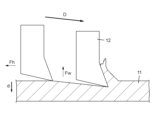
- FIG. 3 is a schematic diagram illustrating a method for measuring the assumed shear strength of a graphite sheet in an embodiment.
- Graphite sheets are used, for example, as a thermally conductive sheet that is sandwiched between a heating element and a heat sink and is in close contact with both the heating element and the heat sink to smoothly transfer heat generated by the heating element to the heat sink.
- General graphite sheets obtained by pyrolyzing and graphitizing polymer films, have high thermal conductivity in the plane direction but low surface compressibility. There are also graphite sheets with high surface compressibility, but their thermal conductivity in the plane direction is low. Even if these graphite sheets are stacked, contact thermal resistance occurs between the sheets, so the heat dissipation performance remains low.
- the inventors conducted extensive research to solve the above-mentioned problems and discovered that heat dissipation performance can be controlled by creating a specific relationship between specific physical property values on both surfaces of the graphite sheet, leading to the completion of the graphite sheet and electronic device disclosed herein.
- FIG. 1 is a schematic cross-sectional view showing the graphite sheet 1 according to this embodiment.
- the graphite sheet 1 in FIG. 1 has a first main surface S1 and a second main surface S2, which is the surface opposite to the first main surface S1.
- the density (hereinafter also referred to as density (II)) of the surface layer portion on the second main surface S2 side of the graphite sheet 1 (hereinafter also referred to as second surface layer T2) is smaller than the density (hereinafter also referred to as density (I)) of the surface layer portion on the first main surface S1 side (hereinafter also referred to as first surface layer T1).
- first main surface S1 side means a position closer to the first main surface S1 than the second main surface S2 when viewed from a plane passing through the center of the thickness of the graphite sheet 1.
- second main surface S2 side means a position closer to the second main surface S2 than the first main surface S1 when viewed from a plane passing through the center of the thickness of the graphite sheet 1.
- the graphite sheet 1 of this embodiment can reduce the contact thermal resistance on the surface and improve the heat dissipation performance.
- the reason why the graphite sheet 1 has the above-mentioned configuration and thus produces the above-mentioned effect is not necessarily clear, but can be inferred as follows, for example.
- the graphite sheet 1 of this embodiment has a density in the surface layer portion that is smaller in the surface layer portion T1 on the second main surface S2 side than in the surface layer portion T2 on the first main surface S1 side. In the second surface layer portion T2 on the second main surface S2 side, the compressibility is greater due to the smaller density.
- the graphite sheet 1 can fully absorb the irregularities. As a result, the contact thermal resistance on the second main surface S2 side can be reduced.
- the density is greater, and therefore the thermal conductivity in the surface direction of the graphite sheet is maintained high. As a result, it is believed that the graphite sheet 1 can improve the heat dissipation performance from the heat generating body 20 etc. to the heat sink 30 etc.
- the graphite sheet 1 is a sheet containing graphite as a main component.
- the term "main component” refers to a component having the highest content, for example, a content of 50% by mass or more, preferably 80% by mass or more, and more preferably 99% by mass or more.
- Graphite is a type of carbon allotrope, and is also called graphite.
- Graphite has a structure in which layers (graphene layers) in which carbon atoms are arranged in a hexagonal honeycomb lattice shape by sp2 bonds are bonded in multiple layers in the thickness direction by van der Waals forces. Examples of graphite include layers of graphite (graphite layers) stacked together.
- the average thickness of the graphite sheet 1 is, for example, 25 ⁇ m or more and 1000 ⁇ m or less, preferably 50 ⁇ m or more and 500 ⁇ m or less, and more preferably 100 ⁇ m or more and 400 ⁇ m or less.
- the graphite sheet 1 has a first surface layer T1 on the first main surface S1 side, and a second surface layer T2 on the second main surface S2 side.
- the "surface layer” of the graphite sheet 1 refers to the region from the surface (the first main surface S1 or the second main surface S2) to a depth of 20 ⁇ m.
- density (II) of second surface layer portion T2 is smaller than density (I) of first surface layer portion T1.
- Density (II) is smaller than density (I) means that density (II) is 0.95 times or less of density (I).
- the "density" of the surface layer portion in graphite sheet 1 refers to the mass value (kg/ m3 ) per certain volume in the surface layer portion, and means the arithmetic average value of multiple density measurements obtained by cutting out multiple (e.g., 10) portions of a certain volume from the surface layer portion and measuring each of them.
- the ratio of density (II) to density (I) is preferably 0.9 or less, more preferably 0.7 or less, and even more preferably 0.5 or less.
- Density (II)/density (I) is, for example, 0.1 or more, and preferably 0.2 or more.
- Graphite sheet 1 as shown in FIG. 1, usually has a dense layer 2 in the first surface portion T1 on the first main surface S1 side.
- Dense layer 2 is a layer (region) where graphite crystallizes and hardens. Dense layer 2 has higher thermal conductivity in the surface direction. This makes it possible to further increase the thermal conductivity in the surface direction on the first main surface S1 side of graphite sheet 1, thereby further improving the heat dissipation performance of graphite sheet 1.
- Dense layer 2 can be formed, for example, by pyrolyzing a polyimide film or the like to obtain a carbonized film, which is then graphitized by baking at about 2600°C.
- the "surface direction” refers to the direction along the surface or the direction parallel to the surface.
- the deemed shear strength is usually smaller in the second surface layer T2 on the second main surface S2 side than in the first surface layer T1 on the first main surface S1 side.
- strength (I) > strength (II).
- Strength (Strength (II) is smaller than strength (I) means that strength (I) is 1.05 times or more stronger than strength (II).
- the second surface layer T2 on the second main surface S2 side of the graphite sheet 1 can be made softer, and the contact thermal resistance on the surface of the second main surface S2 can be further reduced. As a result, the heat dissipation performance of the graphite sheet 1 can be further improved.
- This deemed shear strength is a value measured at a depth of 0.5 ⁇ m to 19 ⁇ m from the surface. A small assumed shear strength indicates a soft state.
- the SAICAS method known as the Surface and Interfacial Cutting Analysis System method, is an evaluation method in which a material is cut from the surface layer at a low speed with a sharp cutting blade.
- Figure 3 is a schematic diagram explaining a method for measuring the deemed shear strength of the surface layer of a graphite sheet.
- the arrow D in Figure 3 indicates oblique cutting, and the arrow d indicates displacement.
- the SAICAS method the horizontal force (Fh) and vertical force (Fw) applied to the cutting blade when cutting the surface of graphite sheet 11 can be measured, and the deemed shear strength of the surface layer can be calculated from the horizontal force (Fh) applied to cutting blade 12, the cutting angle of cutting blade 12, and the cross-sectional area.
- the graphite sheet 11 is fixed to a SAICAS DN-20 (manufactured by Daipla Wintes Co., Ltd.), the cutting edge 12 is made of boron nitride and has a width of 2 mm, a rake angle of 20°, and a clearance angle of 10°, and the cutting speed is set to 0.5 ⁇ m/sec in the horizontal direction and 0.05 ⁇ m/sec in the vertical direction in constant speed mode.
- SAICAS DN-20 manufactured by Daipla Wintes Co., Ltd.
- the cutting edge 12 is made of boron nitride and has a width of 2 mm, a rake angle of 20°, and a clearance angle of 10°
- the cutting speed is set to 0.5 ⁇ m/sec in the horizontal direction and 0.05 ⁇ m/sec in the vertical direction in constant speed mode.
- the point at which the horizontal load reaches 0.002 N or more is taken as the point at which the cutting edge 12 comes into contact with the graphite sheet 11, and measurements are taken from that point in the vertical direction up to 19 ⁇ m, and the deemed shear strength from 0.5 ⁇ m to a depth of 19 ⁇ m is calculated.
- the following formula is used for the calculation:
- the ratio of the strength (I) to the strength (II) is preferably 1.1 or more, and more preferably 1.2 or more.
- the ratio to the intensity (II) is, for example, 2 or less, and preferably 1.7 or less.
- Graphite sheet 1 can be obtained, for example, by pyrolyzing a polyimide film to obtain a carbonized film, which is then graphitized by baking at approximately 2600°C to obtain a graphite sheet having dense layers on both surfaces, and then cutting the graphite sheet into two pieces in a direction parallel to the main surface of the carbonized film.
- Fig. 2 is a cross-sectional view showing an example of electronic device 100 of the present embodiment.
- Electronic device 100 of Fig. 2 includes graphite sheet 1, heating element 20, heat sink 30, and substrate 40.
- Graphite sheet 1 is sandwiched between heating element 20 and heat sink 30. Since electronic device 100 includes graphite sheet 1 of the present embodiment described above, it is possible to improve heat dissipation performance.
- the heating element 20 is a member that generates heat, such as a semiconductor component.
- semiconductor components include, but are not limited to, transistors, CPUs (Central Processing Units), MPUs (Micro Processing Units), driver ICs (Integrated Circuits), and memories.
- the heating element 20 may be composed of, for example, a heat spreader and a chip portion fixed onto the heat spreader.
- the heat spreader is a plate-like member made of metal or the like, and the chip portion is, for example, a semiconductor package. In this case, the chip portion is disposed on a portion of the heat spreader excluding the outer edge portion, and the outer edge portion may have a plurality of screw holes or the like formed therein that penetrate the heat spreader.
- the heat sink 30 is a member to which the heat generated by the heat generating body 20 is transferred. Heat can be released from the heat sink 30.
- the heat sink 30 is, for example, a heat sink.
- the heat sink 30 may further include heat dissipation fins.
- the heat sink 30 may have a plurality of screw holes, etc., formed at positions corresponding to the plurality of screw holes, etc., in the heat generating body 20 described above.
- first main surface S1 and second main surface S2 of graphite sheet 1 sandwiched between heating element 20 and heat sink 30 is not particularly limited.
- first main surface S1 of graphite sheet 1 is in contact with heat sink 30, and second main surface S2 of graphite sheet 1 is in contact with heating element 20.
- the graphite sheet (1) according to the first embodiment has a first main surface (S1) and a second main surface (S2) that is the surface opposite to the first main surface (S1).
- the density of the surface layer (T2) on the second main surface (S2) side of the graphite sheet (1) is smaller than the density of the surface layer (T1) on the first main surface (S1) side.
- the contact thermal resistance on the surface of the graphite sheet (1) can be reduced, and the heat dissipation performance can be improved.
- the graphite sheet (1) in the first embodiment, has a dense layer (2) in the surface layer portion (T1) on the first main surface (S1) side.
- the thermal conductivity in the planar direction on the first main surface (S1) side of the graphite sheet (1) can be further increased, and as a result, the heat dissipation performance of the graphite sheet (1) can be further improved.
- the assumed shear strength of the surface layer of the graphite sheet (1) measured by the SAICAS method is smaller on the second main surface (S2) side than on the first main surface (S1) side.
- the second main surface (S2) of the graphite sheet (1) can be made softer, which can further reduce the contact thermal resistance on the surface of the second main surface, thereby further improving the heat dissipation performance of the graphite sheet (1).
- the electronic device (100) of the fourth aspect includes a graphite sheet (1) of any one of the first to third aspects, a heating element (20), and a heat sink (30).
- the electronic device (100) can improve heat dissipation performance by using a graphite sheet (1) that can reduce the contact thermal resistance on the surface.
- the first main surface (S1) of the graphite sheet (1) is in contact with the heat sink (30), and the second main surface (S2) of the graphite sheet (1) is in contact with the heat generating element (20).
- the graphite sheet (1) can absorb the unevenness of the heating element (20) and further reduce the contact thermal resistance on the surface of the graphite sheet (1) that contacts the heating element (20), thereby further improving the heat dissipation performance of the electronic device (100).
- the graphite sheet and electronic device disclosed herein can reduce the contact thermal resistance on the surface and improve heat dissipation performance, and can realize an electronic device equipped with this graphite sheet. Therefore, the graphite sheet and electronic device disclosed herein are industrially useful.
Landscapes
- Chemical & Material Sciences (AREA)
- Organic Chemistry (AREA)
- Life Sciences & Earth Sciences (AREA)
- General Life Sciences & Earth Sciences (AREA)
- Geology (AREA)
- Inorganic Chemistry (AREA)
- Physics & Mathematics (AREA)
- Thermal Sciences (AREA)
- Engineering & Computer Science (AREA)
- Microelectronics & Electronic Packaging (AREA)
- Cooling Or The Like Of Semiconductors Or Solid State Devices (AREA)
- Cooling Or The Like Of Electrical Apparatus (AREA)
Abstract
L'invention concerne : une feuille de graphite pouvant réduire la résistance thermique de contact sur une surface et améliorer les performances de rayonnement thermique ; et un dispositif électronique comprenant la feuille de graphite. Une feuille de graphite (1) présente une première surface principale (S1) et une seconde surface principale (S2), qui est la surface opposée à la première surface principale (S1). Dans la feuille de graphite (1), la densité d'une partie de couche de surface (partie de couche de seconde surface (T2)) sur le côté seconde surface principale (S2) est inférieure à la densité d'une partie de couche de surface (partie de couche de première surface (T1)) sur le côté première surface principale (S1).
Priority Applications (1)
| Application Number | Priority Date | Filing Date | Title |
|---|---|---|---|
| JP2025526037A JPWO2024252904A1 (fr) | 2023-06-06 | 2024-05-20 |
Applications Claiming Priority (2)
| Application Number | Priority Date | Filing Date | Title |
|---|---|---|---|
| JP2023-093443 | 2023-06-06 | ||
| JP2023093443 | 2023-06-06 |
Publications (1)
| Publication Number | Publication Date |
|---|---|
| WO2024252904A1 true WO2024252904A1 (fr) | 2024-12-12 |
Family
ID=93795463
Family Applications (1)
| Application Number | Title | Priority Date | Filing Date |
|---|---|---|---|
| PCT/JP2024/018469 Ceased WO2024252904A1 (fr) | 2023-06-06 | 2024-05-20 | Feuille de graphite et dispositif électronique |
Country Status (2)
| Country | Link |
|---|---|
| JP (1) | JPWO2024252904A1 (fr) |
| WO (1) | WO2024252904A1 (fr) |
Citations (7)
| Publication number | Priority date | Publication date | Assignee | Title |
|---|---|---|---|---|
| JPS6294830U (fr) * | 1985-12-06 | 1987-06-17 | ||
| JP2002319653A (ja) * | 2001-04-20 | 2002-10-31 | Matsushita Electric Ind Co Ltd | グラファイトシートおよびそれを用いた放熱部品 |
| JP2003092384A (ja) * | 2001-09-19 | 2003-03-28 | Matsushita Electric Ind Co Ltd | グラファイトシート |
| JP2007217206A (ja) * | 2006-02-15 | 2007-08-30 | Kaneka Corp | グラファイトフィルム、およびそれを用いた熱拡散フィルム、ならびにそれを用いた熱拡散方法。 |
| JP2013230975A (ja) * | 2008-01-18 | 2013-11-14 | Kaneka Corp | 多層グラファイトフィルムおよびその製造方法、電子機器、ディスプレイならびにバックライト |
| JP2021128953A (ja) * | 2020-02-10 | 2021-09-02 | 株式会社カネカ | 熱伝導シート、電子デバイス、および電子デバイスの製造方法 |
| WO2022209004A1 (fr) * | 2021-03-30 | 2022-10-06 | パナソニックIpマネジメント株式会社 | Feuille de graphite et son procédé de production |
-
2024
- 2024-05-20 JP JP2025526037A patent/JPWO2024252904A1/ja active Pending
- 2024-05-20 WO PCT/JP2024/018469 patent/WO2024252904A1/fr not_active Ceased
Patent Citations (7)
| Publication number | Priority date | Publication date | Assignee | Title |
|---|---|---|---|---|
| JPS6294830U (fr) * | 1985-12-06 | 1987-06-17 | ||
| JP2002319653A (ja) * | 2001-04-20 | 2002-10-31 | Matsushita Electric Ind Co Ltd | グラファイトシートおよびそれを用いた放熱部品 |
| JP2003092384A (ja) * | 2001-09-19 | 2003-03-28 | Matsushita Electric Ind Co Ltd | グラファイトシート |
| JP2007217206A (ja) * | 2006-02-15 | 2007-08-30 | Kaneka Corp | グラファイトフィルム、およびそれを用いた熱拡散フィルム、ならびにそれを用いた熱拡散方法。 |
| JP2013230975A (ja) * | 2008-01-18 | 2013-11-14 | Kaneka Corp | 多層グラファイトフィルムおよびその製造方法、電子機器、ディスプレイならびにバックライト |
| JP2021128953A (ja) * | 2020-02-10 | 2021-09-02 | 株式会社カネカ | 熱伝導シート、電子デバイス、および電子デバイスの製造方法 |
| WO2022209004A1 (fr) * | 2021-03-30 | 2022-10-06 | パナソニックIpマネジメント株式会社 | Feuille de graphite et son procédé de production |
Also Published As
| Publication number | Publication date |
|---|---|
| JPWO2024252904A1 (fr) | 2024-12-12 |
Similar Documents
| Publication | Publication Date | Title |
|---|---|---|
| CN103547441B (zh) | 高导热性/低热膨胀系数的复合物 | |
| CN104813751B (zh) | 包括块状石墨烯材料的热管理组件 | |
| JP5784261B2 (ja) | 冷却装置及びこれを用いた冷却装置付きパワーモジュール | |
| JP5612471B2 (ja) | 層状熱拡散器およびその製造方法 | |
| JP2011159662A (ja) | 半導体装置 | |
| JP2017123379A (ja) | 半導体装置 | |
| JP4466644B2 (ja) | ヒートシンク | |
| JP2001085877A (ja) | 突起部を有する受熱面を備えたヒートシンク | |
| JP6750379B2 (ja) | 冷却装置 | |
| WO2024252904A1 (fr) | Feuille de graphite et dispositif électronique | |
| CN1802741A (zh) | 半导体装置 | |
| CN111615746A (zh) | 电力电子模块及制造电力电子模块的方法 | |
| JP7788619B2 (ja) | 熱伝導性材料及び電子部品 | |
| JP7201658B2 (ja) | 冷却装置 | |
| CN106992157B (zh) | 半导体装置 | |
| JP7738276B2 (ja) | グラファイトシート及びその製造方法 | |
| JP6849137B1 (ja) | 半導体装置 | |
| JP7662505B2 (ja) | 放熱基板 | |
| WO2026053943A1 (fr) | Stratifié | |
| JP7261602B2 (ja) | 半導体装置及び電力変換装置 | |
| JP2020072219A (ja) | グラファイト構造体 | |
| TW202527296A (zh) | 傳熱構件及電子裝置 | |
| JPWO2023223934A5 (fr) | ||
| CN119108361A (zh) | 半导体装置 | |
| JP2020038887A (ja) | 冷却装置 |
Legal Events
| Date | Code | Title | Description |
|---|---|---|---|
| 121 | Ep: the epo has been informed by wipo that ep was designated in this application |
Ref document number: 24819137 Country of ref document: EP Kind code of ref document: A1 |
|
| ENP | Entry into the national phase |
Ref document number: 2025526037 Country of ref document: JP Kind code of ref document: A |
|
| NENP | Non-entry into the national phase |
Ref country code: DE |