WO2024252904A1 - グラファイトシート及び電子機器 - Google Patents
グラファイトシート及び電子機器 Download PDFInfo
- Publication number
- WO2024252904A1 WO2024252904A1 PCT/JP2024/018469 JP2024018469W WO2024252904A1 WO 2024252904 A1 WO2024252904 A1 WO 2024252904A1 JP 2024018469 W JP2024018469 W JP 2024018469W WO 2024252904 A1 WO2024252904 A1 WO 2024252904A1
- Authority
- WO
- WIPO (PCT)
- Prior art keywords
- graphite sheet
- main surface
- electronic device
- surface layer
- graphite
- Prior art date
- Legal status (The legal status is an assumption and is not a legal conclusion. Google has not performed a legal analysis and makes no representation as to the accuracy of the status listed.)
- Ceased
Links
Images


Classifications
-
- C—CHEMISTRY; METALLURGY
- C01—INORGANIC CHEMISTRY
- C01B—NON-METALLIC ELEMENTS; COMPOUNDS THEREOF; METALLOIDS OR COMPOUNDS THEREOF NOT COVERED BY SUBCLASS C01C
- C01B32/00—Carbon; Compounds thereof
- C01B32/20—Graphite
-
- H—ELECTRICITY
- H05—ELECTRIC TECHNIQUES NOT OTHERWISE PROVIDED FOR
- H05K—PRINTED CIRCUITS; CASINGS OR CONSTRUCTIONAL DETAILS OF ELECTRIC APPARATUS; MANUFACTURE OF ASSEMBLAGES OF ELECTRICAL COMPONENTS
- H05K7/00—Constructional details common to different types of electric apparatus
- H05K7/20—Modifications to facilitate cooling, ventilating, or heating
-
- H—ELECTRICITY
- H10—SEMICONDUCTOR DEVICES; ELECTRIC SOLID-STATE DEVICES NOT OTHERWISE PROVIDED FOR
- H10W—GENERIC PACKAGES, INTERCONNECTIONS, CONNECTORS OR OTHER CONSTRUCTIONAL DETAILS OF DEVICES COVERED BY CLASS H10
- H10W40/00—Arrangements for thermal protection or thermal control
- H10W40/10—Arrangements for heating
-
- H—ELECTRICITY
- H10—SEMICONDUCTOR DEVICES; ELECTRIC SOLID-STATE DEVICES NOT OTHERWISE PROVIDED FOR
- H10W—GENERIC PACKAGES, INTERCONNECTIONS, CONNECTORS OR OTHER CONSTRUCTIONAL DETAILS OF DEVICES COVERED BY CLASS H10
- H10W40/00—Arrangements for thermal protection or thermal control
- H10W40/20—Arrangements for cooling
- H10W40/25—Arrangements for cooling characterised by their materials
Definitions
- This disclosure relates to a graphite sheet and an electronic device, and more particularly to a graphite sheet having two surfaces, and an electronic device including the graphite sheet.
- Power modules such as Insulated Gate Bipolar Transistors (IGBTs) are attached to heat dissipation components with screws or other means to dissipate the heat generated during operation.
- IGBTs Insulated Gate Bipolar Transistors
- a solid heat dissipation sheet is sandwiched between the power module and the heat dissipation components instead of the conventional semi-solid grease, which has low thermal conductivity.
- Patent Document 1 discloses that in a power module with a heat dissipation component, the power module includes a base plate, a ceramic insulating substrate bonded to one surface of the base plate, a semiconductor element bonded to the ceramic insulating substrate, and a heat dissipation component attached to the base plate side of the power module via a heat dissipation sheet, and that the flatness of the surface of the base plate opposite the surface to which the ceramic insulating substrate is bonded is 20 ⁇ m or less.
- Graphite sheets are used as heat dissipation sheets placed between the power modules and heat dissipation components as described above.
- typical graphite sheets obtained by pyrolyzing and graphitizing polymer films, have high thermal conductivity in the plane direction but poor surface compressibility.
- many heat generating elements such as power modules have uneven surfaces. If such graphite sheets are used, the contact thermal resistance between the surface of the heat generating element increases, and there is a possibility that the heat dissipation performance from the heat generating element to the heat sink may decrease.
- the objective of this disclosure is to provide a graphite sheet that can reduce the contact thermal resistance on the surface and improve heat dissipation performance, and an electronic device equipped with this graphite sheet.
- the graphite sheet according to one embodiment of the present disclosure is a graphite sheet having a first main surface and a second main surface opposite the first main surface, and the density of the surface layer on the second main surface side of the graphite sheet is smaller than the density of the surface layer on the first main surface side.
- An electronic device includes the graphite sheet, a heating element, and a heat sink.
- the graphite sheet and electronic device disclosed herein can provide a graphite sheet that can reduce the contact thermal resistance on the surface and improve heat dissipation performance, as well as an electronic device equipped with this graphite sheet.
- FIG. 1 is a schematic cross-sectional view showing a graphite sheet according to an embodiment.
- FIG. 2 is a schematic cross-sectional view illustrating an electronic device according to an embodiment.
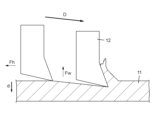
- FIG. 3 is a schematic diagram illustrating a method for measuring the assumed shear strength of a graphite sheet in an embodiment.
- Graphite sheets are used, for example, as a thermally conductive sheet that is sandwiched between a heating element and a heat sink and is in close contact with both the heating element and the heat sink to smoothly transfer heat generated by the heating element to the heat sink.
- General graphite sheets obtained by pyrolyzing and graphitizing polymer films, have high thermal conductivity in the plane direction but low surface compressibility. There are also graphite sheets with high surface compressibility, but their thermal conductivity in the plane direction is low. Even if these graphite sheets are stacked, contact thermal resistance occurs between the sheets, so the heat dissipation performance remains low.
- the inventors conducted extensive research to solve the above-mentioned problems and discovered that heat dissipation performance can be controlled by creating a specific relationship between specific physical property values on both surfaces of the graphite sheet, leading to the completion of the graphite sheet and electronic device disclosed herein.
- FIG. 1 is a schematic cross-sectional view showing the graphite sheet 1 according to this embodiment.
- the graphite sheet 1 in FIG. 1 has a first main surface S1 and a second main surface S2, which is the surface opposite to the first main surface S1.
- the density (hereinafter also referred to as density (II)) of the surface layer portion on the second main surface S2 side of the graphite sheet 1 (hereinafter also referred to as second surface layer T2) is smaller than the density (hereinafter also referred to as density (I)) of the surface layer portion on the first main surface S1 side (hereinafter also referred to as first surface layer T1).
- first main surface S1 side means a position closer to the first main surface S1 than the second main surface S2 when viewed from a plane passing through the center of the thickness of the graphite sheet 1.
- second main surface S2 side means a position closer to the second main surface S2 than the first main surface S1 when viewed from a plane passing through the center of the thickness of the graphite sheet 1.
- the graphite sheet 1 of this embodiment can reduce the contact thermal resistance on the surface and improve the heat dissipation performance.
- the reason why the graphite sheet 1 has the above-mentioned configuration and thus produces the above-mentioned effect is not necessarily clear, but can be inferred as follows, for example.
- the graphite sheet 1 of this embodiment has a density in the surface layer portion that is smaller in the surface layer portion T1 on the second main surface S2 side than in the surface layer portion T2 on the first main surface S1 side. In the second surface layer portion T2 on the second main surface S2 side, the compressibility is greater due to the smaller density.
- the graphite sheet 1 can fully absorb the irregularities. As a result, the contact thermal resistance on the second main surface S2 side can be reduced.
- the density is greater, and therefore the thermal conductivity in the surface direction of the graphite sheet is maintained high. As a result, it is believed that the graphite sheet 1 can improve the heat dissipation performance from the heat generating body 20 etc. to the heat sink 30 etc.
- the graphite sheet 1 is a sheet containing graphite as a main component.
- the term "main component” refers to a component having the highest content, for example, a content of 50% by mass or more, preferably 80% by mass or more, and more preferably 99% by mass or more.
- Graphite is a type of carbon allotrope, and is also called graphite.
- Graphite has a structure in which layers (graphene layers) in which carbon atoms are arranged in a hexagonal honeycomb lattice shape by sp2 bonds are bonded in multiple layers in the thickness direction by van der Waals forces. Examples of graphite include layers of graphite (graphite layers) stacked together.
- the average thickness of the graphite sheet 1 is, for example, 25 ⁇ m or more and 1000 ⁇ m or less, preferably 50 ⁇ m or more and 500 ⁇ m or less, and more preferably 100 ⁇ m or more and 400 ⁇ m or less.
- the graphite sheet 1 has a first surface layer T1 on the first main surface S1 side, and a second surface layer T2 on the second main surface S2 side.
- the "surface layer” of the graphite sheet 1 refers to the region from the surface (the first main surface S1 or the second main surface S2) to a depth of 20 ⁇ m.
- density (II) of second surface layer portion T2 is smaller than density (I) of first surface layer portion T1.
- Density (II) is smaller than density (I) means that density (II) is 0.95 times or less of density (I).
- the "density" of the surface layer portion in graphite sheet 1 refers to the mass value (kg/ m3 ) per certain volume in the surface layer portion, and means the arithmetic average value of multiple density measurements obtained by cutting out multiple (e.g., 10) portions of a certain volume from the surface layer portion and measuring each of them.
- the ratio of density (II) to density (I) is preferably 0.9 or less, more preferably 0.7 or less, and even more preferably 0.5 or less.
- Density (II)/density (I) is, for example, 0.1 or more, and preferably 0.2 or more.
- Graphite sheet 1 as shown in FIG. 1, usually has a dense layer 2 in the first surface portion T1 on the first main surface S1 side.
- Dense layer 2 is a layer (region) where graphite crystallizes and hardens. Dense layer 2 has higher thermal conductivity in the surface direction. This makes it possible to further increase the thermal conductivity in the surface direction on the first main surface S1 side of graphite sheet 1, thereby further improving the heat dissipation performance of graphite sheet 1.
- Dense layer 2 can be formed, for example, by pyrolyzing a polyimide film or the like to obtain a carbonized film, which is then graphitized by baking at about 2600°C.
- the "surface direction” refers to the direction along the surface or the direction parallel to the surface.
- the deemed shear strength is usually smaller in the second surface layer T2 on the second main surface S2 side than in the first surface layer T1 on the first main surface S1 side.
- strength (I) > strength (II).
- Strength (Strength (II) is smaller than strength (I) means that strength (I) is 1.05 times or more stronger than strength (II).
- the second surface layer T2 on the second main surface S2 side of the graphite sheet 1 can be made softer, and the contact thermal resistance on the surface of the second main surface S2 can be further reduced. As a result, the heat dissipation performance of the graphite sheet 1 can be further improved.
- This deemed shear strength is a value measured at a depth of 0.5 ⁇ m to 19 ⁇ m from the surface. A small assumed shear strength indicates a soft state.
- the SAICAS method known as the Surface and Interfacial Cutting Analysis System method, is an evaluation method in which a material is cut from the surface layer at a low speed with a sharp cutting blade.
- Figure 3 is a schematic diagram explaining a method for measuring the deemed shear strength of the surface layer of a graphite sheet.
- the arrow D in Figure 3 indicates oblique cutting, and the arrow d indicates displacement.
- the SAICAS method the horizontal force (Fh) and vertical force (Fw) applied to the cutting blade when cutting the surface of graphite sheet 11 can be measured, and the deemed shear strength of the surface layer can be calculated from the horizontal force (Fh) applied to cutting blade 12, the cutting angle of cutting blade 12, and the cross-sectional area.
- the graphite sheet 11 is fixed to a SAICAS DN-20 (manufactured by Daipla Wintes Co., Ltd.), the cutting edge 12 is made of boron nitride and has a width of 2 mm, a rake angle of 20°, and a clearance angle of 10°, and the cutting speed is set to 0.5 ⁇ m/sec in the horizontal direction and 0.05 ⁇ m/sec in the vertical direction in constant speed mode.
- SAICAS DN-20 manufactured by Daipla Wintes Co., Ltd.
- the cutting edge 12 is made of boron nitride and has a width of 2 mm, a rake angle of 20°, and a clearance angle of 10°
- the cutting speed is set to 0.5 ⁇ m/sec in the horizontal direction and 0.05 ⁇ m/sec in the vertical direction in constant speed mode.
- the point at which the horizontal load reaches 0.002 N or more is taken as the point at which the cutting edge 12 comes into contact with the graphite sheet 11, and measurements are taken from that point in the vertical direction up to 19 ⁇ m, and the deemed shear strength from 0.5 ⁇ m to a depth of 19 ⁇ m is calculated.
- the following formula is used for the calculation:
- the ratio of the strength (I) to the strength (II) is preferably 1.1 or more, and more preferably 1.2 or more.
- the ratio to the intensity (II) is, for example, 2 or less, and preferably 1.7 or less.
- Graphite sheet 1 can be obtained, for example, by pyrolyzing a polyimide film to obtain a carbonized film, which is then graphitized by baking at approximately 2600°C to obtain a graphite sheet having dense layers on both surfaces, and then cutting the graphite sheet into two pieces in a direction parallel to the main surface of the carbonized film.
- Fig. 2 is a cross-sectional view showing an example of electronic device 100 of the present embodiment.
- Electronic device 100 of Fig. 2 includes graphite sheet 1, heating element 20, heat sink 30, and substrate 40.
- Graphite sheet 1 is sandwiched between heating element 20 and heat sink 30. Since electronic device 100 includes graphite sheet 1 of the present embodiment described above, it is possible to improve heat dissipation performance.
- the heating element 20 is a member that generates heat, such as a semiconductor component.
- semiconductor components include, but are not limited to, transistors, CPUs (Central Processing Units), MPUs (Micro Processing Units), driver ICs (Integrated Circuits), and memories.
- the heating element 20 may be composed of, for example, a heat spreader and a chip portion fixed onto the heat spreader.
- the heat spreader is a plate-like member made of metal or the like, and the chip portion is, for example, a semiconductor package. In this case, the chip portion is disposed on a portion of the heat spreader excluding the outer edge portion, and the outer edge portion may have a plurality of screw holes or the like formed therein that penetrate the heat spreader.
- the heat sink 30 is a member to which the heat generated by the heat generating body 20 is transferred. Heat can be released from the heat sink 30.
- the heat sink 30 is, for example, a heat sink.
- the heat sink 30 may further include heat dissipation fins.
- the heat sink 30 may have a plurality of screw holes, etc., formed at positions corresponding to the plurality of screw holes, etc., in the heat generating body 20 described above.
- first main surface S1 and second main surface S2 of graphite sheet 1 sandwiched between heating element 20 and heat sink 30 is not particularly limited.
- first main surface S1 of graphite sheet 1 is in contact with heat sink 30, and second main surface S2 of graphite sheet 1 is in contact with heating element 20.
- the graphite sheet (1) according to the first embodiment has a first main surface (S1) and a second main surface (S2) that is the surface opposite to the first main surface (S1).
- the density of the surface layer (T2) on the second main surface (S2) side of the graphite sheet (1) is smaller than the density of the surface layer (T1) on the first main surface (S1) side.
- the contact thermal resistance on the surface of the graphite sheet (1) can be reduced, and the heat dissipation performance can be improved.
- the graphite sheet (1) in the first embodiment, has a dense layer (2) in the surface layer portion (T1) on the first main surface (S1) side.
- the thermal conductivity in the planar direction on the first main surface (S1) side of the graphite sheet (1) can be further increased, and as a result, the heat dissipation performance of the graphite sheet (1) can be further improved.
- the assumed shear strength of the surface layer of the graphite sheet (1) measured by the SAICAS method is smaller on the second main surface (S2) side than on the first main surface (S1) side.
- the second main surface (S2) of the graphite sheet (1) can be made softer, which can further reduce the contact thermal resistance on the surface of the second main surface, thereby further improving the heat dissipation performance of the graphite sheet (1).
- the electronic device (100) of the fourth aspect includes a graphite sheet (1) of any one of the first to third aspects, a heating element (20), and a heat sink (30).
- the electronic device (100) can improve heat dissipation performance by using a graphite sheet (1) that can reduce the contact thermal resistance on the surface.
- the first main surface (S1) of the graphite sheet (1) is in contact with the heat sink (30), and the second main surface (S2) of the graphite sheet (1) is in contact with the heat generating element (20).
- the graphite sheet (1) can absorb the unevenness of the heating element (20) and further reduce the contact thermal resistance on the surface of the graphite sheet (1) that contacts the heating element (20), thereby further improving the heat dissipation performance of the electronic device (100).
- the graphite sheet and electronic device disclosed herein can reduce the contact thermal resistance on the surface and improve heat dissipation performance, and can realize an electronic device equipped with this graphite sheet. Therefore, the graphite sheet and electronic device disclosed herein are industrially useful.
Landscapes
- Chemical & Material Sciences (AREA)
- Organic Chemistry (AREA)
- Life Sciences & Earth Sciences (AREA)
- General Life Sciences & Earth Sciences (AREA)
- Geology (AREA)
- Inorganic Chemistry (AREA)
- Physics & Mathematics (AREA)
- Thermal Sciences (AREA)
- Engineering & Computer Science (AREA)
- Microelectronics & Electronic Packaging (AREA)
- Cooling Or The Like Of Semiconductors Or Solid State Devices (AREA)
- Cooling Or The Like Of Electrical Apparatus (AREA)
Abstract
表面での接触熱抵抗を低減することができ、放熱性能を向上させることができるグラファイトシート及びこのグラファイトシートを備える電子機器を提供する。グラファイトシート(1)は、第1主面(S1)と、第1主面(S1)とは反対の面である第2主面(S2)とを有する。グラファイトシート(1)における第2主面(S2)側の表層部(第2表層部(T2))の密度は、第1主面(S1)側の表層部(第1表層部(T1))の密度よりも小さい。
Description
本開示は、グラファイトシート及び電子機器に関し、詳しくは、両表面を有するグラファイトシート、及びこのグラファイトシートを備える電子機器に関する。
絶縁ゲートバイポーラトランジスタ(Insulated Gate Bipolar Transistor(IGBT))等のパワーモジュールは、駆動時に発生する熱を逃がすために、放熱部品にネジなどで取り付けられて使用される。このとき、パワーモジュールから放熱部品にスムースに熱を伝えるため、これらの間に、熱伝導性が低く半固体である従来のグリースに代えて、固体の放熱シートを挟むことが行われている。
特許文献1には、ベース板と、前記ベース板の一面上に接合されたセラミックス絶縁基板と、前記セラミックス絶縁基板上に接合された半導体素子と、を備えるパワーモジュールと、前記パワーモジュールの前記ベース板側に放熱シートを介して取り付けられた放熱部品と、を備えた放熱部品付きパワーモジュールにおいて、ベース板のセラミックス絶縁基板が接合された面と反対側の面の平面度を20μm以下とすることが開示されている。
上記のようなパワーモジュールと放熱部品との間に配置される放熱シートとして、グラファイトシートが用いられている。しかし、高分子フィルムを熱分解しグラファイト化して得られる一般的なグラファイトシートは、面方向の熱伝導性は高いものの、表面の圧縮性に乏しい。また、パワーモジュール等の発熱体には、その面に凹凸を有するものが多い。このようなグラファイトシートを用いたのでは、発熱体の面等との間の接触熱抵抗が大きくなり、発熱体から放熱体への放熱性能が低くなる可能性がある。
本開示の課題は、表面での接触熱抵抗を低減させることができ、放熱性能を向上させることができるグラファイトシート、及びこのグラファイトシートを備える電子機器を提供することである。
本開示の一態様に係るグラファイトシートは、第1主面と、前記第1主面とは反対側の第2主面とを有するグラファイトシートであって、前記グラファイトシートにおける前記第2主面側の表層部の密度は、前記第1主面側の表層部の密度よりも小さい。
本開示の他の一態様に係る電子機器は、前記グラファイトシートと、発熱体と、放熱体とを備える。
本開示のグラファイトシート及び電子機器によれば、表面での接触熱抵抗を低減させることができ、放熱性能を向上させることができるグラファイトシート、及びこのグラファイトシートを備える電子機器を提供することができる。
1.概要
以下、本開示の実施形態におけるグラファイトシートについて説明する。なお、以下の実施形態は、本開示の様々な実施形態の一つに過ぎない。以下の実施形態は、本開示の目的を達成できれば、設計に応じて種々の変更が可能である。
以下、本開示の実施形態におけるグラファイトシートについて説明する。なお、以下の実施形態は、本開示の様々な実施形態の一つに過ぎない。以下の実施形態は、本開示の目的を達成できれば、設計に応じて種々の変更が可能である。
グラファイトシートは、例えば、発熱体と放熱体との間に挟み、発熱体及び放熱体に密着させて、発熱体で発生した熱を放熱体にスムースに伝える熱伝導シートとして用いられる。
高分子フィルムを熱分解しグラファイト化して得られる一般的なグラファイトシートは、面方向の熱伝導性は高いものの、表面の圧縮性は低い。表面の圧縮性を高くしたグラファイトシートもあるが、面方向の熱伝導性は低いものになっている。また、これらのグラファイトシートを重ねて使用しても、シート間の接触熱抵抗が生じるため、放熱性能は低いものに留まる。
発明者らは、前述の課題を解決すべく、鋭意検討を重ねる上で、グラファイトシートの両表面における特定の物性値を特定の関係とすることで、放熱性能を制御できることを見出し、本開示のグラファイトシート及び電子機器を完成させた。
本開示の実施形態のグラファイトシート1の一例を、図1に示す。図1は、本実施形態に係るグラファイトシート1を示す模式的断面図である。図1のグラファイトシート1は、第1主面S1と、第1主面S1とは反対の面である第2主面S2とを有している。グラファイトシート1における第2主面S2側の表層部(以下、第2表層部T2ともいう)の密度(以下、密度(II)ともいう)は、第1主面S1側の表層部(以下、第1表層部T1ともいう)の密度(以下、密度(I)ともいう)よりも小さい。「第1主面S1側」とは、グラファイトシート1の厚さの中央を通る面からみて第2主面S2よりも第1主面S1のほうに近い位置であることを意味する。また、「第2主面S2側」とは、グラファイトシート1の厚さの中央を通る面からみて第1主面S1よりも第2主面S2のほうに近い位置であることを意味する。
本実施形態のグラファイトシート1によれば、表面での接触熱抵抗を低減させることができ、放熱性能を向上させることができる。グラファイトシート1が、前記構成を備えることで、前記効果を奏する理由については、必ずしも明確ではないが、例えば以下のように推察することができる。本実施形態のグラファイトシート1は、表層部における密度について、第2主面S2側における表層部T1の密度を、第1主面S1側における表層部T2の密度よりも小さくしている。第2主面S2側の第2表層部T2においては、密度がより小さいことに起因して、圧縮性は大きくなっている。これにより、グラファイトシート1は、第2主面S2に接触して配置される発熱体20等の面に凹凸がある場合でも、この凹凸を十分に吸収することができる。その結果、第2主面S2側における接触熱抵抗を低減させることができる。一方、第1主面S1側の第1表層部T1においては、密度がより大きいことに起因して、グラファイトシートが有する面方向の熱伝導性が高く維持される。これらにより、グラファイトシート1は、発熱体20等から放熱体30等への放熱性能を向上させることができると考えられる。
2.詳細
<グラファイトシート>
グラファイトシート1は、グラファイトを主成分とするシートである。「主成分」とは、最も含有率が大きい成分をいい、例えば50質量%以上、好ましくは80質量%以上、より好ましくは99質量%以上の含有率の成分をいう。グラファイトは、炭素の同素体の一種である黒鉛のことであり、石墨ともいう。グラファイトは、炭素原子がsp2結合により六角形のハニカム格子状に配置された層(グラフェン層)が、ファンデルワールス力により、厚さ方向に複数層結合した構造を有している。グラファイトとしては、例えばグラファイトからなる層(グラファイト層)が複数層積層したもの等も含まれる。
<グラファイトシート>
グラファイトシート1は、グラファイトを主成分とするシートである。「主成分」とは、最も含有率が大きい成分をいい、例えば50質量%以上、好ましくは80質量%以上、より好ましくは99質量%以上の含有率の成分をいう。グラファイトは、炭素の同素体の一種である黒鉛のことであり、石墨ともいう。グラファイトは、炭素原子がsp2結合により六角形のハニカム格子状に配置された層(グラフェン層)が、ファンデルワールス力により、厚さ方向に複数層結合した構造を有している。グラファイトとしては、例えばグラファイトからなる層(グラファイト層)が複数層積層したもの等も含まれる。
グラファイトシート1の平均厚さは、例えば25μm以上かつ1000μm以下であり、50μm以上かつ500μm以下であることが好ましく、100μm以上かつ400μm以下であることがより好ましい。
グラファイトシート1は、図1に示すように、第1主面S1側に、第1表層部T1を有し、第2主面S2側に、第2表層部T2を有している。グラファイトシート1における「表層部」とは、表面(第1主面S1又は第2主面S2)から、深さ20μmまでの領域をいう。
グラファイトシート1において、第2表層部T2の密度(II)は、第1表層部T1の密度(I)よりも小さいことが重要である。「密度(II)が密度(I)よりも小さい」とは、密度(II)が密度(I)の0.95倍以下であることを意味する。グラファイトシート1における表層部の「密度」とは、表層部における一定体積あたりの質量の値(kg/m3)をいい、表層部中の複数(例えば10点)の一定体積の部分を切り取ってそれぞれ測定した複数の密度測定値の算術平均値を意味する。
密度(II)の密度(I)に対する比(密度(II)/密度(I))は、0.9以下であることが好ましく、0.7以下であることがより好ましく、0.5以下であることがさらに好ましい。密度(II)/密度(I)は、例えば0.1以上であり、0.2以上であることが好ましい。
グラファイトシート1は、図1に示すように、第1主面S1側の第1表層部T1に、通常、緻密層2を有している。緻密層2は、グラファイトの結晶化が進み、硬くなった層(領域)である。緻密層2においては、面方向の熱伝導性がより高くなっている。このため、グラファイトシート1の第1主面S1側における面方向の熱伝導性をより高めることができ、その結果、グラファイトシート1の放熱性能をより向上させることができる。緻密層2は、例えば、ポリイミドフィルム等を熱分解することにより得られた炭化フィルムを、さらに約2600℃で焼成してグラファイト化すること等により、形成させることができる。なお、「面方向」とは、面に沿う方向または面に平行な方向である。
グラファイトシート1の表層部をSAICAS法により測定したときのみなしせん断強度は、通常、第1主面S1側の第1表層部T1よりも第2主面S2側の第2表層部T2のほうが小さくなっている。すなわち、第1表層部T1のみなしせん断強度を強度(I)とし、第2表層部T2のみなしせん断強度を強度(II)としたとき、強度(I)>強度(II)である。「強度(I)よりも強度(II)が小さい」とは、強度(I)が強度(II)の1.05倍以上であることを意味する。この場合、グラファイトシート1の第2主面S2側の第2表層部T2をより柔らかくすることができ、それにより、第2主面S2の表面での接触熱抵抗をより低減させることができる。その結果、グラファイトシート1の放熱性能をより向上させることができる。このみなしせん断強度は、表面から0.5μmから19μmまでの深さにおいて測定した値である。みなしせん断強度が小さいことは、柔らかい状態であることを示す。
SAICAS法とは、Surface And Interfacial Cutting Analysis System法と呼ばれる、材料を表層から鋭利な切刃で低速で切削する評価方法である。図3は、グラファイトシートの表層におけるみなしせん断強度の測定方法を説明する模式図である。図3のDの矢印は斜め切削であること、dの矢印は変位を意味する。SAICAS法を用いることによって、グラファイトシート11の表面の切削時に切刃に加わる水平力(Fh)と垂直力(Fw)を測定することができ、切刃12に加わる水平力(Fh)と切刃12の切込み角度、及び断面積から表層におけるみなしせん断強度を算出することができる。具体的には、SAICAS DN-20(ダイプラ・ウィンテス株式会社製)にグラファイトシート11を固定し、切刃12には窒化硼素(ボロンナイトライド)製の幅が2mm、すくい角が20°、逃げ角が10°の刃を用い、切削速度は定速度モードで水平方向が0.5μm/秒、垂直方向が0.05μm/秒とする。水平荷重が0.002N以上となった点を切刃12がグラファイトシート11に接触した点とし、そこから垂直方向に19μmまで測定し、0.5μmから19μmまでの深さまでのみなしせん断強度を計算する。計算式は以下の式を用いる。
t=Fh×(2A×Cot(φ))
(t:みなしせん断強度、Fh:水平力、A:切削切刃の断面積、φ:せん断角度)
強度(I)の強度(II)に対する比(強度(I)/強度(II))は、1.1以上であることが好ましく、1.2以上であることがより好ましい。強度(I)の強度(II)に対する比は、例えば2以下であり、1.7以下であることが好ましい。
(t:みなしせん断強度、Fh:水平力、A:切削切刃の断面積、φ:せん断角度)
強度(I)の強度(II)に対する比(強度(I)/強度(II))は、1.1以上であることが好ましく、1.2以上であることがより好ましい。強度(I)の強度(II)に対する比は、例えば2以下であり、1.7以下であることが好ましい。
グラファイトシート1は、例えば、ポリイミドフィルムを熱分解することにより炭化フィルムを得た後、さらに約2600℃で焼成してグラファイト化することにより得られる両方の表層に緻密層を有するグラファイトシートを、炭化フィルムの主面に平行な方向に2つに切断することなどにより得ることができる。
<電子機器>
図2は、本実施形態の電子機器100の一例を示す断面図である。図2の電子機器100は、グラファイトシート1と、発熱体20と、放熱体30と、基板40とを備えている。グラファイトシート1は、発熱体20と放熱体30との間に挟まれている。電子機器100は、上述の本実施形態のグラファイトシート1を備えているので、放熱性能を向上させることができる。
図2は、本実施形態の電子機器100の一例を示す断面図である。図2の電子機器100は、グラファイトシート1と、発熱体20と、放熱体30と、基板40とを備えている。グラファイトシート1は、発熱体20と放熱体30との間に挟まれている。電子機器100は、上述の本実施形態のグラファイトシート1を備えているので、放熱性能を向上させることができる。
発熱体20は、熱を発する部材であり、例えば半導体部品である。半導体部品としては、例えばトランジスタ、CPU(Central Processing Unit)、MPU(Micro Processing Unit)、ドライバIC(Integrated Circuit)、メモリ等が挙げられるが、これらに限定されない。発熱体20は、例えばヒートスプレッダと、ヒートスプレッダ上に固定されたチップ部とから構成されていてもよい。ヒートスプレッダは、金属等から作製された板状の部材であり、チップ部は、例えば半導体パッケージである。この場合、チップ部は、ヒートスプレッダの外縁部を除く部分の上に配置され、外縁部には、ヒートスプレッダを貫通する複数のネジ穴等が形成されていてもよい。
放熱体30は、発熱体20が発した熱が伝達される部材である。放熱体30から熱が放出され得る。放熱体30は、例えばヒートシンクである。放熱体30が板状のヒートシンクである場合、放熱体30は、さらに放熱フィンを備えていてもよい。放熱体30には、前述の発熱体20における複数のネジ穴等にそれぞれ対応する位置に、複数のネジ穴等が形成されていてもよい。
電子機器100において、発熱体20と放熱体30との間に挟まれるグラファイトシート1の、第1主面S1および第2主面S2の向きは特に限定されない。図2の電子機器100において、グラファイトシート1の第1主面S1が放熱体30と接触し、グラファイトシート1の第2主面S2が発熱体20と接触している。電子機器100において、グラファイトシートの両面をこのような向きとすることで、発熱体20の凹凸をより吸収して、表面での接触熱抵抗をより低減することができ、電子機器100の放熱性能をより向上させることができる。
3.態様
上記実施形態から明らかなように、本開示は、下記の態様を含む。以下では、実施形態との対応関係を明示するためだけに、符号を括弧付きで付している。
上記実施形態から明らかなように、本開示は、下記の態様を含む。以下では、実施形態との対応関係を明示するためだけに、符号を括弧付きで付している。
第1の態様に係るグラファイトシート(1)は、第1主面(S1)と、第1主面(S1)とは反対の面である第2主面(S2)とを有する。グラファイトシート(1)における第2主面(S2)側の表層部(T2)の密度は、第1主面(S1)側の表層部(T1)の密度よりも小さい。
第1の態様によれば、グラファイトシート(1)の表面での接触熱抵抗を低減することができ、放熱性能を向上させることができる。
第2の態様に係るグラファイトシート(1)では、第1の態様において、グラファイトシート(1)は、第1主面(S1)側の表層部(T1)に緻密層(2)を有する。
第2の態様によれば、グラファイトシート(1)の第1主面(S1)側における面方向の熱伝導性をより高めることができ、その結果、グラファイトシート(1)の放熱性能をより向上させることができる。
第3の態様に係るグラファイトシート(1)では、第1又は第2の態様において、グラファイトシート(1)の表層部をSAICAS法により測定したときのみなしせん断強度が、第1主面(S1)側よりも第2主面(S2)側のほうが小さい。
第3の態様によれば、グラファイトシート(1)の第2主面(S2)をより柔らかくすることができ、それにより、第2主面の表面での接触熱抵抗をより低減させることができ、その結果、グラファイトシート(1)の放熱性能をより向上させることができる。
第4の態様に係る電子機器(100)は、第1から第3の態様のいずれか一つに係るグラファイトシート(1)と、発熱体(20)と、放熱体(30)とを備える。
第4の態様によれば、電子機器(100)は、表面での接触熱抵抗を低減させることができるグラファイトシート(1)を用いることにより、放熱性能を向上させることができる。
第5の態様に係る電子機器(100)では、第4の態様において、グラファイトシート(1)の第1主面(S1)が放熱体(30)と接触し、グラファイトシート(1)の第2主面(S2)が発熱体(20)と接触している。
第5の態様によれば、グラファイトシート(1)が、発熱体(20)の凹凸を吸収して、発熱体(20)に接するグラファイトシート(1)の表面での接触熱抵抗をより低減することができ、電子機器(100)の放熱性能をより向上させることができる。
本開示のグラファイトシート及び電子機器は、表面での接触熱抵抗を低減させることができ、放熱性能を向上させることができるグラファイトシート、及びこのグラファイトシートを備える電子機器を実現できる。そのため、本開示のグラファイトシート及び電子機器は、産業上有用である。
1、11 グラファイトシート
S1 第1主面
S2 第2主面
T1 第1表層部
T2 第2表層部
2 緻密層
20 発熱体
30 放熱体
100 電子機器
S1 第1主面
S2 第2主面
T1 第1表層部
T2 第2表層部
2 緻密層
20 発熱体
30 放熱体
100 電子機器
Claims (5)
- 第1主面と、前記第1主面とは反対の面である第2主面とを有するグラファイトシートであって、
前記グラファイトシートにおける前記第2主面側の表層部の密度は、前記第1主面側の表層部の密度よりも小さい、
グラファイトシート。 - 前記グラファイトシートは、前記第1主面側の前記表層部に緻密層を有する、
請求項1に記載のグラファイトシート。 - 前記グラファイトシートの前記第1主面側の前記表層部および前記第2主面側の前記表層部をSAICAS法により測定したときのみなしせん断強度が、前記第1主面側の前記表層部よりも前記第2主面側の前記表層部のほうが小さい、
請求項1に記載のグラファイトシート。 - 請求項1から請求項3のいずれか一項に記載のグラファイトシートと、
発熱体と、
放熱体と
を備える電子機器。 - 前記グラファイトシートの前記第1主面が前記放熱体と接触し、
前記グラファイトシートの前記第2主面が前記発熱体と接触している、
請求項4に記載の電子機器。
Priority Applications (1)
| Application Number | Priority Date | Filing Date | Title |
|---|---|---|---|
| JP2025526037A JPWO2024252904A1 (ja) | 2023-06-06 | 2024-05-20 |
Applications Claiming Priority (2)
| Application Number | Priority Date | Filing Date | Title |
|---|---|---|---|
| JP2023-093443 | 2023-06-06 | ||
| JP2023093443 | 2023-06-06 |
Publications (1)
| Publication Number | Publication Date |
|---|---|
| WO2024252904A1 true WO2024252904A1 (ja) | 2024-12-12 |
Family
ID=93795463
Family Applications (1)
| Application Number | Title | Priority Date | Filing Date |
|---|---|---|---|
| PCT/JP2024/018469 Ceased WO2024252904A1 (ja) | 2023-06-06 | 2024-05-20 | グラファイトシート及び電子機器 |
Country Status (2)
| Country | Link |
|---|---|
| JP (1) | JPWO2024252904A1 (ja) |
| WO (1) | WO2024252904A1 (ja) |
Citations (7)
| Publication number | Priority date | Publication date | Assignee | Title |
|---|---|---|---|---|
| JPS6294830U (ja) * | 1985-12-06 | 1987-06-17 | ||
| JP2002319653A (ja) * | 2001-04-20 | 2002-10-31 | Matsushita Electric Ind Co Ltd | グラファイトシートおよびそれを用いた放熱部品 |
| JP2003092384A (ja) * | 2001-09-19 | 2003-03-28 | Matsushita Electric Ind Co Ltd | グラファイトシート |
| JP2007217206A (ja) * | 2006-02-15 | 2007-08-30 | Kaneka Corp | グラファイトフィルム、およびそれを用いた熱拡散フィルム、ならびにそれを用いた熱拡散方法。 |
| JP2013230975A (ja) * | 2008-01-18 | 2013-11-14 | Kaneka Corp | 多層グラファイトフィルムおよびその製造方法、電子機器、ディスプレイならびにバックライト |
| JP2021128953A (ja) * | 2020-02-10 | 2021-09-02 | 株式会社カネカ | 熱伝導シート、電子デバイス、および電子デバイスの製造方法 |
| WO2022209004A1 (ja) * | 2021-03-30 | 2022-10-06 | パナソニックIpマネジメント株式会社 | グラファイトシート及びその製造方法 |
-
2024
- 2024-05-20 JP JP2025526037A patent/JPWO2024252904A1/ja active Pending
- 2024-05-20 WO PCT/JP2024/018469 patent/WO2024252904A1/ja not_active Ceased
Patent Citations (7)
| Publication number | Priority date | Publication date | Assignee | Title |
|---|---|---|---|---|
| JPS6294830U (ja) * | 1985-12-06 | 1987-06-17 | ||
| JP2002319653A (ja) * | 2001-04-20 | 2002-10-31 | Matsushita Electric Ind Co Ltd | グラファイトシートおよびそれを用いた放熱部品 |
| JP2003092384A (ja) * | 2001-09-19 | 2003-03-28 | Matsushita Electric Ind Co Ltd | グラファイトシート |
| JP2007217206A (ja) * | 2006-02-15 | 2007-08-30 | Kaneka Corp | グラファイトフィルム、およびそれを用いた熱拡散フィルム、ならびにそれを用いた熱拡散方法。 |
| JP2013230975A (ja) * | 2008-01-18 | 2013-11-14 | Kaneka Corp | 多層グラファイトフィルムおよびその製造方法、電子機器、ディスプレイならびにバックライト |
| JP2021128953A (ja) * | 2020-02-10 | 2021-09-02 | 株式会社カネカ | 熱伝導シート、電子デバイス、および電子デバイスの製造方法 |
| WO2022209004A1 (ja) * | 2021-03-30 | 2022-10-06 | パナソニックIpマネジメント株式会社 | グラファイトシート及びその製造方法 |
Also Published As
| Publication number | Publication date |
|---|---|
| JPWO2024252904A1 (ja) | 2024-12-12 |
Similar Documents
| Publication | Publication Date | Title |
|---|---|---|
| CN103547441B (zh) | 高导热性/低热膨胀系数的复合物 | |
| CN104813751B (zh) | 包括块状石墨烯材料的热管理组件 | |
| JP5784261B2 (ja) | 冷却装置及びこれを用いた冷却装置付きパワーモジュール | |
| JP5612471B2 (ja) | 層状熱拡散器およびその製造方法 | |
| JP2011159662A (ja) | 半導体装置 | |
| JP2017123379A (ja) | 半導体装置 | |
| JP4466644B2 (ja) | ヒートシンク | |
| JP2001085877A (ja) | 突起部を有する受熱面を備えたヒートシンク | |
| JP6750379B2 (ja) | 冷却装置 | |
| WO2024252904A1 (ja) | グラファイトシート及び電子機器 | |
| CN1802741A (zh) | 半导体装置 | |
| CN111615746A (zh) | 电力电子模块及制造电力电子模块的方法 | |
| JP7788619B2 (ja) | 熱伝導性材料及び電子部品 | |
| JP7201658B2 (ja) | 冷却装置 | |
| CN106992157B (zh) | 半导体装置 | |
| JP7738276B2 (ja) | グラファイトシート及びその製造方法 | |
| JP6849137B1 (ja) | 半導体装置 | |
| JP7662505B2 (ja) | 放熱基板 | |
| WO2026053943A1 (ja) | 積層体 | |
| JP7261602B2 (ja) | 半導体装置及び電力変換装置 | |
| JP2020072219A (ja) | グラファイト構造体 | |
| TW202527296A (zh) | 傳熱構件及電子裝置 | |
| JPWO2023223934A5 (ja) | ||
| CN119108361A (zh) | 半导体装置 | |
| JP2020038887A (ja) | 冷却装置 |
Legal Events
| Date | Code | Title | Description |
|---|---|---|---|
| 121 | Ep: the epo has been informed by wipo that ep was designated in this application |
Ref document number: 24819137 Country of ref document: EP Kind code of ref document: A1 |
|
| ENP | Entry into the national phase |
Ref document number: 2025526037 Country of ref document: JP Kind code of ref document: A |
|
| NENP | Non-entry into the national phase |
Ref country code: DE |