WO2024252981A1 - Dispositif d'inspection de substrat, procédé d'inspection de substrat et support d'enregistrement - Google Patents
Dispositif d'inspection de substrat, procédé d'inspection de substrat et support d'enregistrement Download PDFInfo
- Publication number
- WO2024252981A1 WO2024252981A1 PCT/JP2024/019522 JP2024019522W WO2024252981A1 WO 2024252981 A1 WO2024252981 A1 WO 2024252981A1 JP 2024019522 W JP2024019522 W JP 2024019522W WO 2024252981 A1 WO2024252981 A1 WO 2024252981A1
- Authority
- WO
- WIPO (PCT)
- Prior art keywords
- substrate
- light
- wafer
- image
- unit
- Prior art date
- Legal status (The legal status is an assumption and is not a legal conclusion. Google has not performed a legal analysis and makes no representation as to the accuracy of the status listed.)
- Ceased
Links
Images


Classifications
-
- G—PHYSICS
- G01—MEASURING; TESTING
- G01N—INVESTIGATING OR ANALYSING MATERIALS BY DETERMINING THEIR CHEMICAL OR PHYSICAL PROPERTIES
- G01N21/00—Investigating or analysing materials by the use of optical means, i.e. using sub-millimetre waves, infrared, visible or ultraviolet light
- G01N21/84—Systems specially adapted for particular applications
- G01N21/88—Investigating the presence of flaws or contamination
- G01N21/95—Investigating the presence of flaws or contamination characterised by the material or shape of the object to be examined
- G01N21/956—Inspecting patterns on the surface of objects
-
- H—ELECTRICITY
- H10—SEMICONDUCTOR DEVICES; ELECTRIC SOLID-STATE DEVICES NOT OTHERWISE PROVIDED FOR
- H10P—GENERIC PROCESSES OR APPARATUS FOR THE MANUFACTURE OR TREATMENT OF DEVICES COVERED BY CLASS H10
- H10P74/00—Testing or measuring during manufacture or treatment of wafers, substrates or devices
Definitions
- This disclosure relates to a substrate inspection device, a substrate inspection method, and a storage medium.
- the technology disclosed herein improves the accuracy of defect detection in defect inspections based on captured images of substrates.
- One aspect of the present disclosure is a substrate inspection device that inspects a substrate based on an image of the substrate, the device comprising: a holding unit that holds the substrate; a light source unit that emits light to the substrate held in the holding unit; a moving mechanism that moves the holding unit; an imaging unit that images the substrate by receiving reflected or scattered light from the substrate held in the holding unit; and a control unit, the control unit executing the steps of (A) moving the holding unit in a first direction, causing the imaging unit to receive a first light from the substrate held in the holding unit, and imaging the substrate; and (B) thereafter, moving the holding unit in a second direction opposite to the first direction, causing the imaging unit to receive a second light, different from the first light, from the substrate held in the holding unit, and imaging the substrate.
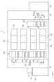
- Fig. 1 is a plan view showing an outline of the configuration of a wafer processing system 1 equipped with a substrate inspection device according to a first embodiment.
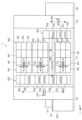
- Figs. 2 and 3 are schematic diagrams showing an outline of the internal configuration of the front side and rear side, respectively, of the wafer processing system 1. Note that, in the following, an example will be described in which the wafer processing system 1 is a coating and developing processing system that performs a coating and developing process on a wafer W.
- the wafer processing system 1 is, for example, a coating and developing processing system that performs coating and developing processing on wafers W. As shown in FIG. 1, the wafer processing system 1 has a cassette station 10 where cassettes C containing multiple wafers W are loaded and unloaded, and a processing station 11 equipped with multiple types of processing equipment that perform predetermined processing on the wafers W.
- the wafer processing system 1 has a configuration in which the cassette station 10, the processing station 11, and an interface station 13 that transfers the wafers W between them and an exposure device 12 adjacent to the opposite side of the processing station 11 are integrally connected.
- the cassette station 10 is provided with a cassette placement table 20.
- the cassette placement table 20 is provided with a plurality of placement plates 21 on which the cassette C is placed when the cassette C is transported in and out of the wafer processing system 1.
- the cassette station 10 is provided with a wafer transport device 23 that is movable on a transport path 22 that extends in the X direction.
- the wafer transport device 23 is also movable in the vertical direction and around the vertical axis ( ⁇ direction), and can transport wafers W between the cassettes C on each mounting plate 21 and a transfer device in the third block G3 of the processing station 11, which will be described later.
- the processing station 11 is provided with multiple, for example, four, blocks G1, G2, G3, and G4 equipped with various devices.
- a first block G1 is provided on the front side of the processing station 11 (negative side in the X direction in FIG. 1)
- a second block G2 is provided on the rear side of the processing station 11 (positive side in the X direction in FIG. 1).
- a third block G3 is provided on the cassette station 10 side of the processing station 11 (negative side in the Y direction in FIG. 1)
- a fourth block G4 is provided on the interface station 13 side of the processing station 11 (positive side in the Y direction in FIG. 1).
- a plurality of liquid processing devices for example, a development processing device 30, a lower anti-reflective film forming device 31, a resist coating device 32, and an upper anti-reflective film forming device 33, are arranged in this order from the bottom.
- the development processing device 30 develops the wafer W, and the lower anti-reflective film forming device 31 forms an anti-reflective film (hereinafter referred to as "lower anti-reflective film”) on the lower layer of the resist film of the wafer W.
- the resist coating device 32 applies a resist liquid to the wafer W to form a resist film, and the upper anti-reflective film forming device 33 forms an anti-reflective film (hereinafter referred to as "upper anti-reflective film”) on the upper layer of the resist film of the wafer W.
- upper anti-reflective film an anti-reflective film
- each of the development processing device 30, lower anti-reflective film forming device 31, resist coating device 32, and upper anti-reflective film forming device 33 are arranged horizontally.
- the number and arrangement of these development processing device 30, lower anti-reflective film forming device 31, resist coating device 32, and upper anti-reflective film forming device 33 can be selected arbitrarily.
- multiple transfer devices 50, 51, 52, 53, 54, 55, and 56 are provided in order from the bottom.
- multiple transfer devices 60, 61, and 62 and an inspection device 63 as a substrate inspection device are provided in order from the bottom. The configuration of the inspection device 63 will be described later.
- the wafer transport device 70 has a transport arm 70a that can move, for example, in the Y direction, X direction, ⁇ direction, and up and down.
- the wafer transport device 70 moves within the wafer transport area D and can transport the wafer W to a predetermined unit within the surrounding first block G1, second block G2, third block G3, and fourth block G4.
- multiple wafer transport devices 70 are arranged vertically as shown in FIG. 3, and can transport the wafer W to a predetermined device at approximately the same height in each of the blocks G1 to G4.
- a shuttle transport device 80 is provided in the wafer transport area D to transport the wafer W linearly between the third block G3 and the fourth block G4.
- the shuttle transfer device 80 is movable linearly, for example, in the Y direction in FIG. 3.
- the shuttle transfer device 80 moves in the Y direction while supporting the wafer W, and can transfer the wafer W between the transfer device 52 in the third block G3 and the transfer device 62 in the fourth block G4.
- a wafer transport device 90 is provided next to the third block G3 on the positive side in the X direction.
- the wafer transport device 90 has a transport arm 90a that can move, for example, in the X direction, the ⁇ direction, and the vertical direction.
- the wafer transport device 90 can move up and down while supporting a wafer W, and transport the wafer W to each transfer device in the third block G3.
- the interface station 13 is provided with a wafer transport device 100 and a transfer device 101.
- the wafer transport device 100 has a transfer arm 100a that is movable, for example, in the Y direction, the ⁇ direction, and the up and down directions.
- the wafer transport device 100 can support a wafer W on the transfer arm 100a, for example, and transfer the wafer W between each transfer device in the fourth block G4, the transfer device 101, and the exposure device 12.
- the above wafer processing system 1 is provided with at least one control unit 200 as shown in FIG. 1.
- the control unit 200 processes computer-executable instructions that cause the wafer processing system 1 to perform the various steps described in this disclosure.
- the control unit 200 may be configured to control each element of the wafer processing system 1 to perform the various steps described herein. In one embodiment, a part or all of the control unit 200 may be included in the wafer processing system 1.
- the control unit 200 may include a processing unit, a storage unit, and a communication interface.
- the control unit 200 is realized, for example, by a computer.
- the processing unit may be configured to read a program that provides logic or routines that enable various control operations to be performed from the storage unit, and to perform various control operations by executing the read program.
- This program may be stored in the storage unit in advance, or may be acquired via a medium when necessary.
- the acquired program is stored in the storage unit, and is read from the storage unit by the processing unit and executed.
- the medium may be various storage media readable by a computer, or may be a communication line connected to the communication interface.
- the storage medium may be a temporary storage medium or a non-temporary storage medium H.
- the processing unit may be a CPU (Central Processing Unit) or one or more circuits.
- the storage unit may include a RAM (Random Access Memory), a ROM (Read Only Memory), a HDD (Hard Disk Drive), an SSD (Solid State Drive), or a combination thereof.
- the communication interface may communicate with the wafer processing system 1 via a communication line such as a LAN (Local Area Network).
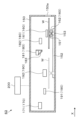
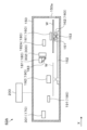
- the inspection device 63 has a housing 150.
- One side wall of the housing 150 is formed with a loading/unloading opening 150a for loading and unloading the wafer W into and from the housing 150.
- a wafer chuck 151 that holds a wafer W is provided inside the housing 150. That is, the housing 150 accommodates the wafer chuck 151.
- a guide rail 152 is provided on the bottom surface of the housing 150, extending from the front side (positive side of the X direction in FIG. 4) to the back side (negative side of the X direction in FIG. 4) of the housing 150.
- a drive unit 153 that rotates the wafer chuck 151 and is movable along the guide rail 152 is provided on the guide rail 152.
- the drive unit 153 has a drive source (not shown) such as a motor that generates a drive force for rotating the wafer chuck 151 and a drive force for moving the drive unit 153.
- the wafer W held by the wafer chuck 151 can be moved by the drive unit 153 between a first position near the loading/unloading port 150a, i.e., on the front side, and a second position near the peripheral imaging unit 190 described later, i.e., on the back side.
- This drive unit 153 constitutes at least a part of the movement mechanism that moves the wafer chuck 151.
- an aligner unit 160 is provided within the housing 150.
- the aligner unit 160 is provided at the front side within the housing 150.
- the aligner unit 160 has a light-projecting unit 161 at either the top or bottom, and a light-receiving unit 162 at the other.
- the light-projecting unit 161 includes, for example, an LED.
- the light-receiving unit 162 includes, for example, a PD (Photodiode).
- the aligner unit 160 is provided so that the peripheral portion of the wafer W held by the wafer chuck 151 and positioned at the first position described above can be sandwiched between the light-projecting unit 161 and the light-receiving unit 162.
- the control unit 200 detects the position of the notch formed on the peripheral edge of the wafer W. After the notch position is detected, the drive unit 153 rotates the wafer chuck 151, so that the wafer W, whose notch position has been detected, can be oriented in a predetermined direction.
- a surface imaging unit 170 Also provided within the housing 150 are a surface imaging unit 170 and a surface light source unit 180.
- the surface imaging unit 170 captures an image of the wafer W held by the wafer chuck 151 by receiving reflected light or scattered light from the wafer W.
- the surface imaging unit 170 has a camera 171.
- Camera 171 is provided, for example, at the upper end of the rear side (the negative X-direction side in FIG. 4) of housing 150, and has a lens (not shown) and an imaging device (not shown) such as a line sensor.
- the camera 171 serves as both a first imaging unit and a second imaging unit.
- the first imaging unit images the wafer W by receiving, as the first light, reflected light from the wafer W held on the wafer chuck 151 (specifically, reflected light from the surface of the wafer W), i.e., bright field light.
- the second imaging unit images the wafer W by receiving, as the second light, scattered light from the wafer W held on the wafer chuck 151 (specifically, scattered light from the surface of the wafer W), i.e., dark field light.
- the image captured by the camera 171 is output to the control unit 200 .
- the surface light source unit 180 emits light to the wafer W held by the wafer chuck 151.
- This surface light source unit 180 has a first light source unit 181 and a second light source unit 182.
- the first light source unit 181 is provided at the top at the center in the depth direction (X direction in the figure) within the housing 150, and a half mirror 183 is provided below the first light source unit 181.
- the half mirror 183 is provided in a position facing the camera 171, with the mirror surface tilted 45 degrees upward toward the camera 171 from a state in which the mirror surface faces vertically downward.
- the illumination from the first light source unit 181 passes through the half mirror 183 and is irradiated downward.
- the light that passes through the half mirror 183 is reflected by an object below the half mirror 183, is further reflected by the half mirror 183, and is received by the camera 171.
- the first light source unit 181 is bright field illumination, and the camera 171 can capture an image of an object in the area illuminated by the first light source unit 181. Therefore, when the wafer chuck 151 holding the wafer W moves along the guide rail 152, the camera 171 can capture an image of the surface of the wafer W passing through the irradiation area of the first light source unit 181.
- the second light source unit 182 is provided above the first light source unit 181 in the housing 150 at a position closer to the user (positive X-direction side in the figure). Illumination from the second light source unit 182 is directed diagonally downward.
- the light irradiation area by the second light source unit 182 and the light irradiation area by the first light source unit 181 are approximately the same. That is, for example, the second light source unit 182 illuminates the area below the half mirror 183.
- the light from the second light source unit 182 is scattered by an object below the half mirror 183, reflected by the half mirror 183, and received by the camera 171.
- the second light source unit 182 is a dark field illumination
- the camera 171 can capture an image of an object in the irradiation area by the second light source unit 182. Therefore, when the wafer chuck 151 holding the wafer W moves along the guide rail 152, the camera 171 can capture an image of the surface of the wafer W passing through the irradiation area of the second light source unit 182.
- a peripheral imaging unit 190 is provided within the housing 150 .
- the peripheral imaging unit 190 is provided, for example, on the rear side (the negative side in the X direction in FIG. 4) within the housing 150, and includes a camera 191, an illumination module 192, and a mirror member (not shown).
- Camera 191 has a lens (not shown) and an imaging element (not shown) such as a line sensor. The image captured by camera 191 is output to control unit 200.
- the lighting module 192 and the mirror member are configured so that, when the wafer W held by the wafer chuck 151 is in the second position, both the light emitted from the lighting module 192 and reflected by the peripheral portion of the surface of the wafer W, and the light emitted from the lighting module 192 and reflected by the side end surface of the wafer W are received by the camera 191.
- the camera 191 can capture images of both the peripheral portion of the surface of the wafer W and the side end surface of the wafer W.
- the peripheral imaging unit 190 captures an image in synchronization with the rotation of the wafer chuck 151 that holds the wafer W. This allows an image to be obtained that is substantially scanned in the circumferential direction of the wafer W for the entire peripheral portion of the wafer W, specifically, for the entire peripheral portion of the front surface of the wafer W and the entire side end surface of the wafer W.
- Fig. 6 is a flow chart for explaining the inspection of the wafer W by the inspection device 63, which is included in the above-mentioned wafer processing.
- a cassette C containing multiple wafers W is placed on a predetermined loading plate 21 of the cassette station 10. Then, under the control of the control unit 200, the wafers W are removed from the cassette C by the wafer transfer device 23 and transferred to, for example, the transfer device 52 in the third block G3 of the processing station 11.
- the wafer W is transported by the wafer transport device 70 to the heat treatment device 40 in the second block G2, where it is subjected to temperature adjustment processing.
- the wafer W is then transported by the wafer transport device 70 to, for example, the lower anti-reflection film forming device 31 in the first block G1, where a lower anti-reflection film is formed on the wafer W.
- the wafer W is then transported to the heat treatment device 40 for the lower layer film in the second block G2, where the lower layer film is subjected to heat processing.
- the wafer W is transferred to the resist coating device 32 in the first block G1, where a resist film is formed on the underlayer film of the wafer W.
- the wafer W is transferred to the heat treatment device 40 for PAB treatment in the second block G2, where the PAB treatment is performed.
- the wafer W is transferred to the upper anti-reflection film forming device 33 in the first block G1, where an upper anti-reflection film is formed on the wafer W.
- the wafer W is transferred to the heat treatment device 40 for the upper layer film in the second block G2, where the upper layer film is heated.
- the wafer W is transported by the wafer transport device 70 to the transfer device 52, and then by the shuttle transport device 80 to the transfer device 62 in the fourth block G4.
- the wafer W is then transported by the wafer transport device 100 in the interface station 13 to the inspection device 63, and loaded into the housing 150.
- the wafer W that has been brought into the housing 150 is placed on the wafer chuck 151 that has been moved to the front side within the housing 150 under the control of the control unit 200.
- the wafer W is carried into the housing 150 to the rear side. Specifically, the wafer W held by the wafer chuck 151 is moved along the guide rails 152 from the first position to the second position described above. At the first position, as described above, the position of the notch of the wafer W is detected, and the wafer W is oriented in a predetermined direction based on the detection result.
- the peripheral imaging unit 190 images the wafer W. Specifically, the peripheral imaging unit 190 images the peripheral portion of the surface of the wafer W and the side end surface of the wafer W.
- the wafer W is removed from the rear side of the housing 150 and moved to the front side of the housing 150.
- the wafer W is then removed from the housing 150 by the wafer transfer device 100 in the inspection device 63.
- the control unit 200 receives the image of the wafer W from the second position to the first position along the depth direction.
- the first light source unit 181 and the second light source unit 182 of the surface light source unit 180 are turned on.
- an image of the surface of the wafer W is captured by the camera 171 of the surface imaging unit 170.
- the imaging result by the surface imaging unit 170 is output to the control unit 200, and an image of the wafer W captured using dark field light (specifically, an image of the surface of the wafer W) is acquired by the control unit 200.
- the method for inspecting the wafer W according to the present embodiment inspects the wafer W based on an image of the wafer W captured by bright field light and an image of the wafer W captured by dark field light. Specifically, the method for inspecting the wafer W according to the present embodiment inspects the wafer W for defects based on the image of the wafer W captured by bright field light (hereinafter referred to as bright field inspection) and inspects the wafer W for defects based on the image of the wafer W captured by dark field light (hereinafter referred to as dark field inspection).
- the image of the wafer W captured by bright field light and the image of the wafer W captured by dark field light are acquired while the wafer W makes one round trip within the housing 150.
- the time required to acquire both images can be shortened compared to acquiring either an image of the wafer W captured by bright field light or an image of the wafer W captured by dark field light while the wafer W makes one round trip within the housing 150, and acquiring the other image while the wafer W makes another round trip within the housing 150. Therefore, according to this embodiment, it is possible to prevent the time required to acquire an image of the wafer W used for defect inspection of the wafer W from becoming long.
- control unit 200 performs both a defect inspection of the surface of the wafer W based on an image of the wafer W captured with bright field light, i.e., a bright field inspection, and a defect inspection of the surface of the wafer W based on an image of the wafer W captured with dark field light, i.e., a dark field inspection.
- the control unit 200 may estimate the cause of defects on the wafer W based on bright-field inspection and dark-field inspection.
- the control unit 200 estimates that the cause of the detected defect on the wafer W is poor coating, scratches, etc. Furthermore, if a defect is detected only by bright field inspection, it is assumed that the defect is present in the film, and therefore the control unit 200 presumes that foreign matter or bubbles in the coating liquid used to form the film are the cause of the detected defect on the wafer W.
- the thickness of the film on the wafer W can be determined, for example, based on a processing recipe stored in a memory unit (not shown). Information relating the defect detection results to their causes is stored in advance in the memory unit (not shown) and is referenced by the control unit 200 when estimating the cause of the defect.
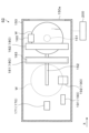
- FIG. 7 is a vertical sectional view showing the outline of the configuration of an inspection device 63A serving as a board inspection device according to the second embodiment.
- the camera 171 of the front-side imaging unit 170 serves as both the first imaging unit and the second imaging unit described above.
- the front-side imaging unit 170A has a camera 301 as the first imaging unit and a camera 302 as the second imaging unit.
- the light irradiation area by the second light source unit 182 for dark field light coincides with the light irradiation area by the first light source unit 181 for bright field light.
- the light irradiation area by the second light source unit 182A for dark field light does not coincide with the light irradiation area by the first light source unit 181 for bright field light.
- the light irradiation area by the second light source unit 182A for dark field light is located in front of the light irradiation area by the first light source unit 181 for bright field light (the positive X-direction side in FIG. 7).
- the front surface imaging unit 170A captures an image of the wafer W under the control of the control unit 200.
- the wafer chuck 151 is moved in a first direction toward the rear of the housing 150 (the negative X direction in FIG. 4), while the bright field light from the wafer W held on the wafer chuck 151 is received by the front surface imaging unit 170A to capture an image of the wafer W.
- the wafer W which has been oriented in a predetermined direction at the first position, is moved along the depth direction to the second position while only the first light source unit 181A and the second light source unit 182A of the surface light source unit 180 are turned on.
- an image of the surface of the wafer W is captured by the camera 301 of the surface imaging unit 170A.
- the image captured by the camera 301 is output to the control unit 200, and an image of the wafer W captured using bright field light (specifically, an image of the surface of the wafer W) is acquired by the control unit 200.
- the wafer chuck 151 After imaging while moving toward the back of the housing 150 as described above, under the control of the control unit 200, the wafer chuck 151 is moved toward the front of the housing 150 (the positive X direction in FIG. 4), which is a second direction opposite to the first direction, while the dark field light from the wafer W held on the wafer chuck 151 is received by the front surface imaging unit 170A to image the wafer W.
- control unit 200 inspects the wafer W based on both images.
- ⁇ Modification 1 of the second embodiment> using the surface imaging unit 170A, one image of the wafer W is acquired using bright field light as the first light when the wafer W moves toward the back of the housing 150 (hereinafter abbreviated as "when moving toward the back"), and one image of the wafer W is acquired using dark field light as the second light when the wafer W moves toward the front of the housing 150 (hereinafter abbreviated as "when moving toward the front"), for a total of two images.
- a total of four images may be acquired by using the front surface imaging unit 170A to capture both an image of the wafer W captured by bright field light and an image of the wafer W captured by dark field light during each of the backward and forward movements. Then, the control unit 200 may inspect the wafer W based on the four captured images.
- the arrangement of the wafer W held by the wafer chuck 151 relative to the front surface imaging unit 170A does not differ between the time of movement in the rear direction and the time of movement in the front direction.
- the arrangement of the wafer W relative to the front surface imaging unit 170A may differ between the time of movement in the rear direction and the time of movement in the front direction, that is, the wafer W held by the wafer chuck 151 may be shifted relative to the front surface imaging unit 170A.
- the arrangement of the wafer W relative to the front surface imaging unit 170A is, for example, the orientation of the wafer W relative to the front surface imaging unit 170A. Specifically, the orientation of the wafer W relative to the front surface imaging unit 170A may be shifted by 45° between the time of movement in the rear direction and the time of movement in the front direction.
- the "positioning of the wafer W relative to the front surface imaging unit 170A" that is different when moving in the depth direction and when moving in the front direction may be the position of the wafer W in the perpendicular direction.
- the position of the wafer W held by the wafer chuck 151 in the perpendicular direction is shifted by half the pitch of the imaging elements of the line cameras that make up the cameras 301 and 302 when moving in the depth direction and when moving in the front direction.
- the above-mentioned "positioning of the wafer W relative to the front-surface imaging unit 170A" may be the angle of the top surface of the wafer chuck 151 relative to the horizontal plane, i.e., the angle of the surface of the wafer W relative to the horizontal plane.
- the position of the wafer W held by the wafer chuck 151 may be different when moving backward and forward.
- both the captured image of the wafer W using bright field light and the captured image of the wafer W using dark field light are acquired during each of the movement in the rearward direction and the movement in the forward direction.
- both the captured image of the wafer W using bright field light and the captured image of the wafer W using dark field light may be acquired only during either the movement in the rearward direction or the movement in the forward direction, and either one of the captured image of the wafer W using bright field light and the captured image of the wafer W using dark field light may be acquired during the other.
- a defect may be detected based on an image of the wafer W obtained by receiving one of the bright field light and dark field light obtained during the movement in the depth direction, i.e., a first defect detection is performed, and a defect may be detected based on an image of the wafer W obtained by the above one of the light receiving results obtained during the movement in the depth direction, i.e., a second defect detection is performed. Then, a defect detected by only one of the first defect detection and the second defect detection may be excluded from the defect detection result as a pseudo defect. In other words, when there are two images of the wafer W obtained by using the same illumination method, a defect detected based only on one of the images may be excluded from the defect detection result as a pseudo defect.
- both an image of the wafer W captured by bright field light and an image of the wafer W captured by dark field light are acquired only when moving in either the backward direction or the forward direction, and neither image needs to be acquired when moving in the other direction.
- the wafer W is moved back and forth only once in the housing 150.
- the wafer W may be moved back and forth again in the housing 150 according to the result of the inspection of the wafer W based on the captured image of the wafer W acquired in the first reciprocation, and an image of the wafer W may be acquired at that time, and the wafer W may be inspected again based on the acquired image.
- the arrangement of the wafer W with respect to the front surface imaging units 170 and 170A may be different between the movement in the back direction and the movement in the front direction.
- the position of the wafer W with respect to the front surface imaging units 170, 170A may be different between the first reciprocation and the second reciprocation.
- both defect detection based on an image of the wafer W captured with bright field light and defect detection based on an image of the wafer W captured with dark field light are performed. Then, if a defect is detected only in one of the two, only the bright field light or dark field light used for the captured image in which the defect was detected may be used for the third and subsequent wafers W.
- the first light is bright field light and the second light is dark field light, but the first light may be dark field light and the second light may be bright field light.
- the first light and the second light may be lights having different amounts of light received by the front-side imaging unit due to an aperture of the front-side imaging unit.
- defects that cannot be detected when only light with a small aperture and a large amount of light is used can be detected.
- the life of the light source can be extended compared to when only light with a large aperture and a small amount of light is used.
- an image of the wafer W may be acquired with light having a small aperture and a large amount of light when moving in the rearward direction, and a coarse defect inspection of the wafer W may be performed based on the acquired image, and only when a defect is detected, an image of the wafer W may be acquired with light having a large aperture and a small amount of light when moving in the forward direction. Then, a fine defect inspection of the wafer W may be performed based on the acquired image.
- An angle adjustment mechanism may be provided for adjusting the relative angle of light from the front surface light source unit with respect to the wafer W held on the wafer chuck 151.
- the angle adjustment mechanism may adjust the angle of the optical axis of the front surface light source unit, or may adjust the angle of the wafer mounting surface of the wafer chuck 151.
- the defect detection rate changes depending on the incident angle of the light with respect to the wafer W, so that the defect detection rate can be improved by providing the angle adjustment mechanism as described above.
- a substrate inspection device that inspects a substrate based on a captured image of the substrate, comprising: A holder for holding the substrate; a light source unit that emits light toward the substrate held by the holder; A moving mechanism that moves the holding unit; an imaging unit that images the substrate by receiving reflected light or scattered light from the substrate held by the holding unit; A control unit, The control unit is (A) moving the holding unit in a first direction while receiving a first light from the substrate held by the holding unit with the imaging unit to image the substrate; (B) then, while moving the holding portion in a second direction opposite to the first direction, the imaging portion receives a second light different from the first light from the substrate held by the holding portion, thereby imaging the substrate.
- the substrate inspection apparatus according to (1) wherein one of the first light and the second light is bright field light, and the other is dark field light.
- the substrate inspection apparatus according to (1), wherein the first light and the second light have different wavelength bands.
- the imaging unit has an aperture, The substrate inspection apparatus according to (1), wherein the first light and the second light are received by the imaging unit in amounts different from each other through the aperture.
- the light source unit includes a first light source unit for the first light and a second light source unit for the second light.
- the imaging unit includes a first imaging unit that receives the first light and a second imaging unit that receives the second light.
- the holding portion is moved while the first light and the second light from the substrate held by the holding portion are received by the first imaging portion and the second imaging portion, respectively, to image the substrate.
- the control unit of the substrate inspection apparatus described in (8) detects defects on the substrate based on an image of the substrate obtained during movement in the first direction in process (A) and an image of the substrate obtained during movement in the second direction in process (B).
- control unit (C) detecting defects on the substrate based on an image of the substrate captured as a result of receiving the first light; and (D) detecting defects on the substrate based on an image of the substrate captured by receiving the second light; and (E) a step of estimating a cause of the defect on the substrate based on the results of the steps (C) and (D).
- the control unit (F) detecting defects on the substrate based on an image of the substrate captured by receiving one of the first light and the second light obtained in the (A) step; (G) detecting defects on the substrate based on an image of the substrate obtained by the one light receiving result in the (B) step; (H) a step of excluding defects detected in only one of the steps (F) and (G) from the defect detection results.
- a substrate inspection device that inspects a substrate based on a captured image of the substrate, comprising: A holder for holding the substrate; a light source unit that emits light toward the substrate held by the holder; A moving mechanism that moves the holding unit; an imaging unit that images the substrate by receiving reflected light or scattered light from the substrate held by the holding unit; A control unit, The control unit is A substrate inspection device that performs a process of moving the holding portion in a predetermined direction, receiving a first light from the substrate held in the holding portion with the imaging portion to image the substrate, and receiving a second light, different from the first light, from the substrate held in the holding portion with the imaging portion to image the substrate.
- a method for inspecting a substrate based on an image of the substrate comprising: (a) moving a holder that holds the substrate in a first direction, receiving a first light from the substrate held by the holder with an imaging unit, and capturing an image of the substrate; (b) then, while moving the holding portion in a second direction opposite to the first direction, receiving a second light different from the first light from the substrate held by the holding portion with the imaging portion, and imaging the substrate.
- the imaging section includes a first imaging section that receives the first light and a second imaging section that receives the second light.
- the holding portion is moved while the first light and the second light from the substrate held by the holding portion are received by the first imaging portion and the second imaging portion, respectively, to image the substrate.
- One of the first light and the second light is bright field light, and the other is dark field light; (c) detecting defects on the substrate based on an image of the substrate captured as a result of receiving the first light; and (d) detecting defects on the substrate based on an image of the substrate captured as a result of receiving the second light; and (e) a step of estimating a cause of the defect on the substrate based on the results of the steps (C) and (D).
- a readable computer storage medium storing a program that operates on a computer of a control unit that controls a substrate inspection apparatus so as to cause the substrate inspection apparatus to execute a method for inspecting a substrate based on an image of the substrate, the program comprising: The method comprises: a step of receiving a first light from the substrate held by a holding unit with an imaging unit while moving the holding unit that holds the substrate in a first direction, and capturing an image of the substrate; Then, while moving the holding portion in a second direction opposite to the first direction, the imaging portion receives a second light different from the first light from the substrate held by the holding portion, and images the substrate.
Landscapes
- Physics & Mathematics (AREA)
- Health & Medical Sciences (AREA)
- Life Sciences & Earth Sciences (AREA)
- Chemical & Material Sciences (AREA)
- Analytical Chemistry (AREA)
- Biochemistry (AREA)
- General Health & Medical Sciences (AREA)
- General Physics & Mathematics (AREA)
- Immunology (AREA)
- Pathology (AREA)
- Investigating Materials By The Use Of Optical Means Adapted For Particular Applications (AREA)
- Testing Or Measuring Of Semiconductors Or The Like (AREA)
Abstract
L'invention concerne un dispositif d'inspection de substrat qui est pour l'inspection d'un substrat sur la base d'une image capturée du substrat, et comprend : une unité de retenue qui retient le substrat ; une unité source de lumière qui émet une lumière vers le substrat retenu par l'unité de retenue ; un mécanisme de déplacement qui déplace l'unité de retenue ; une unité de capture d'image qui capture une image du substrat par la réception d'une lumière réfléchie ou d'une lumière diffusée provenant du substrat retenu par l'unité de retenue ; et une unité de commande. L'unité de commande exécute (A) une étape consistant à amener l'unité d'imagerie à recevoir une première lumière provenant du substrat retenu par l'unité de retenue, tout en déplaçant l'unité de retenue dans une première direction, à capturer une image du substrat, et, par la suite, (B) une étape consistant à amener l'unité d'imagerie à recevoir une seconde lumière différente de la première lumière provenant du substrat retenu par l'unité de retenue, tout en déplaçant l'unité de retenue dans une seconde direction opposée à la première direction, pour capturer une image du substrat.
Applications Claiming Priority (2)
| Application Number | Priority Date | Filing Date | Title |
|---|---|---|---|
| JP2023094658A JP2024176244A (ja) | 2023-06-08 | 2023-06-08 | 基板検査装置、基板検査方法及び記憶媒体 |
| JP2023-094658 | 2023-06-08 |
Publications (1)
| Publication Number | Publication Date |
|---|---|
| WO2024252981A1 true WO2024252981A1 (fr) | 2024-12-12 |
Family
ID=93795928
Family Applications (1)
| Application Number | Title | Priority Date | Filing Date |
|---|---|---|---|
| PCT/JP2024/019522 Ceased WO2024252981A1 (fr) | 2023-06-08 | 2024-05-28 | Dispositif d'inspection de substrat, procédé d'inspection de substrat et support d'enregistrement |
Country Status (3)
| Country | Link |
|---|---|
| JP (1) | JP2024176244A (fr) |
| TW (1) | TW202524080A (fr) |
| WO (1) | WO2024252981A1 (fr) |
Citations (9)
| Publication number | Priority date | Publication date | Assignee | Title |
|---|---|---|---|---|
| JPS6242039A (ja) * | 1985-08-19 | 1987-02-24 | Toshiba Corp | 表面検査装置 |
| JP2005308615A (ja) * | 2004-04-23 | 2005-11-04 | Olympus Corp | 表面欠陥検査装置 |
| JP2007101239A (ja) * | 2005-09-30 | 2007-04-19 | Hitachi Chem Co Ltd | 外観検査装置及び外観検査方法 |
| JP2009080064A (ja) * | 2007-09-27 | 2009-04-16 | Nuflare Technology Inc | パターン検査装置及びパターン検査方法 |
| JP2010032265A (ja) * | 2008-07-25 | 2010-02-12 | Canon Inc | 異物検査装置、露光装置及びデバイス製造方法 |
| JP2012181135A (ja) * | 2011-03-02 | 2012-09-20 | Kobelco Kaken:Kk | 内部欠陥検査装置および内部欠陥検査方法 |
| KR20160068228A (ko) * | 2014-12-05 | 2016-06-15 | 세메스 주식회사 | 웨이퍼 결함 검사 장치 |
| JP2016528478A (ja) * | 2013-06-04 | 2016-09-15 | ケーエルエー−テンカー コーポレイション | 欠陥検出を強化するための最良の開口及びモードを発見するための装置及び方法 |
| JP2020190457A (ja) * | 2019-05-21 | 2020-11-26 | 株式会社昭和電気研究所 | ウエハ検査装置 |
-
2023
- 2023-06-08 JP JP2023094658A patent/JP2024176244A/ja active Pending
-
2024
- 2024-05-27 TW TW113119495A patent/TW202524080A/zh unknown
- 2024-05-28 WO PCT/JP2024/019522 patent/WO2024252981A1/fr not_active Ceased
Patent Citations (9)
| Publication number | Priority date | Publication date | Assignee | Title |
|---|---|---|---|---|
| JPS6242039A (ja) * | 1985-08-19 | 1987-02-24 | Toshiba Corp | 表面検査装置 |
| JP2005308615A (ja) * | 2004-04-23 | 2005-11-04 | Olympus Corp | 表面欠陥検査装置 |
| JP2007101239A (ja) * | 2005-09-30 | 2007-04-19 | Hitachi Chem Co Ltd | 外観検査装置及び外観検査方法 |
| JP2009080064A (ja) * | 2007-09-27 | 2009-04-16 | Nuflare Technology Inc | パターン検査装置及びパターン検査方法 |
| JP2010032265A (ja) * | 2008-07-25 | 2010-02-12 | Canon Inc | 異物検査装置、露光装置及びデバイス製造方法 |
| JP2012181135A (ja) * | 2011-03-02 | 2012-09-20 | Kobelco Kaken:Kk | 内部欠陥検査装置および内部欠陥検査方法 |
| JP2016528478A (ja) * | 2013-06-04 | 2016-09-15 | ケーエルエー−テンカー コーポレイション | 欠陥検出を強化するための最良の開口及びモードを発見するための装置及び方法 |
| KR20160068228A (ko) * | 2014-12-05 | 2016-06-15 | 세메스 주식회사 | 웨이퍼 결함 검사 장치 |
| JP2020190457A (ja) * | 2019-05-21 | 2020-11-26 | 株式会社昭和電気研究所 | ウエハ検査装置 |
Also Published As
| Publication number | Publication date |
|---|---|
| TW202524080A (zh) | 2025-06-16 |
| JP2024176244A (ja) | 2024-12-19 |
Similar Documents
| Publication | Publication Date | Title |
|---|---|---|
| US10460998B2 (en) | Method for inspecting substrate, substrate inspection apparatus, exposure system, and method for producing semiconductor device | |
| TWI487897B (zh) | A substrate processing apparatus, a substrate processing method, a program and a computer memory medium | |
| TWI676799B (zh) | 基板之檢查方法、基板處理系統及電腦記錄媒體 | |
| US10352875B2 (en) | Inspection apparatus, inspection method, exposure method, and method for manufacturing semiconductor device | |
| KR20170098695A (ko) | 기판 처리 방법, 기판 처리 장치 및 컴퓨터 판독 가능한 기록 매체 | |
| TWI800586B (zh) | 基板處理裝置及基板處理方法 | |
| CN109427609B (zh) | 半导体晶片在线检验的系统及方法 | |
| JPWO2012081587A1 (ja) | 検査方法、検査装置、露光管理方法、露光システムおよび半導体デバイス | |
| US20130100441A1 (en) | Optical inspection apparatus and edge inspection device | |
| US20040063232A1 (en) | Surface inspection method, surface inspection apparatus, and recording medium and data signal for providing surface inspection program | |
| JP7157580B2 (ja) | 基板検査方法及び基板検査装置 | |
| JP4385419B2 (ja) | 外観検査方法及び外観検査装置 | |
| JP7090005B2 (ja) | 基板処理装置及び検査方法 | |
| JP4914854B2 (ja) | 欠陥検査方法、プログラム及びコンピュータ記憶媒体 | |
| KR102749664B1 (ko) | 기판 처리 장치 및 검사 방법 | |
| TW202344832A (zh) | 基板檢查裝置,基板檢查方法及基板檢查程式 | |
| WO2024252981A1 (fr) | Dispositif d'inspection de substrat, procédé d'inspection de substrat et support d'enregistrement | |
| JP5825268B2 (ja) | 基板検査装置 | |
| KR20230095989A (ko) | 휨양 추정 장치 및 휨양 추정 방법 | |
| JP2022015474A (ja) | 検査装置及び基板搬送方法 | |
| JP2020025118A (ja) | 基板処理方法、基板処理装置及びコンピュータ読み取り可能な記録媒体 | |
| JP2026069901A (ja) | 基板処理方法、及び、基板処理装置 | |
| JP2025109030A (ja) | 基板撮像装置、基板撮像方法、及び記憶媒体 | |
| TW202536549A (zh) | 描繪裝置以及描繪方法 | |
| JP2025030184A (ja) | 基板エッジ検出方法 |
Legal Events
| Date | Code | Title | Description |
|---|---|---|---|
| 121 | Ep: the epo has been informed by wipo that ep was designated in this application |
Ref document number: 24819212 Country of ref document: EP Kind code of ref document: A1 |
|
| NENP | Non-entry into the national phase |
Ref country code: DE |