WO2024252981A1 - 基板検査装置、基板検査方法及び記憶媒体 - Google Patents
基板検査装置、基板検査方法及び記憶媒体 Download PDFInfo
- Publication number
- WO2024252981A1 WO2024252981A1 PCT/JP2024/019522 JP2024019522W WO2024252981A1 WO 2024252981 A1 WO2024252981 A1 WO 2024252981A1 JP 2024019522 W JP2024019522 W JP 2024019522W WO 2024252981 A1 WO2024252981 A1 WO 2024252981A1
- Authority
- WO
- WIPO (PCT)
- Prior art keywords
- substrate
- light
- wafer
- image
- unit
- Prior art date
- Legal status (The legal status is an assumption and is not a legal conclusion. Google has not performed a legal analysis and makes no representation as to the accuracy of the status listed.)
- Ceased
Links
Images


Classifications
-
- G—PHYSICS
- G01—MEASURING; TESTING
- G01N—INVESTIGATING OR ANALYSING MATERIALS BY DETERMINING THEIR CHEMICAL OR PHYSICAL PROPERTIES
- G01N21/00—Investigating or analysing materials by the use of optical means, i.e. using sub-millimetre waves, infrared, visible or ultraviolet light
- G01N21/84—Systems specially adapted for particular applications
- G01N21/88—Investigating the presence of flaws or contamination
- G01N21/95—Investigating the presence of flaws or contamination characterised by the material or shape of the object to be examined
- G01N21/956—Inspecting patterns on the surface of objects
-
- H—ELECTRICITY
- H10—SEMICONDUCTOR DEVICES; ELECTRIC SOLID-STATE DEVICES NOT OTHERWISE PROVIDED FOR
- H10P—GENERIC PROCESSES OR APPARATUS FOR THE MANUFACTURE OR TREATMENT OF DEVICES COVERED BY CLASS H10
- H10P74/00—Testing or measuring during manufacture or treatment of wafers, substrates or devices
Definitions
- This disclosure relates to a substrate inspection device, a substrate inspection method, and a storage medium.
- the technology disclosed herein improves the accuracy of defect detection in defect inspections based on captured images of substrates.
- One aspect of the present disclosure is a substrate inspection device that inspects a substrate based on an image of the substrate, the device comprising: a holding unit that holds the substrate; a light source unit that emits light to the substrate held in the holding unit; a moving mechanism that moves the holding unit; an imaging unit that images the substrate by receiving reflected or scattered light from the substrate held in the holding unit; and a control unit, the control unit executing the steps of (A) moving the holding unit in a first direction, causing the imaging unit to receive a first light from the substrate held in the holding unit, and imaging the substrate; and (B) thereafter, moving the holding unit in a second direction opposite to the first direction, causing the imaging unit to receive a second light, different from the first light, from the substrate held in the holding unit, and imaging the substrate.
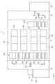
- Fig. 1 is a plan view showing an outline of the configuration of a wafer processing system 1 equipped with a substrate inspection device according to a first embodiment.
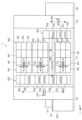
- Figs. 2 and 3 are schematic diagrams showing an outline of the internal configuration of the front side and rear side, respectively, of the wafer processing system 1. Note that, in the following, an example will be described in which the wafer processing system 1 is a coating and developing processing system that performs a coating and developing process on a wafer W.
- the wafer processing system 1 is, for example, a coating and developing processing system that performs coating and developing processing on wafers W. As shown in FIG. 1, the wafer processing system 1 has a cassette station 10 where cassettes C containing multiple wafers W are loaded and unloaded, and a processing station 11 equipped with multiple types of processing equipment that perform predetermined processing on the wafers W.
- the wafer processing system 1 has a configuration in which the cassette station 10, the processing station 11, and an interface station 13 that transfers the wafers W between them and an exposure device 12 adjacent to the opposite side of the processing station 11 are integrally connected.
- the cassette station 10 is provided with a cassette placement table 20.
- the cassette placement table 20 is provided with a plurality of placement plates 21 on which the cassette C is placed when the cassette C is transported in and out of the wafer processing system 1.
- the cassette station 10 is provided with a wafer transport device 23 that is movable on a transport path 22 that extends in the X direction.
- the wafer transport device 23 is also movable in the vertical direction and around the vertical axis ( ⁇ direction), and can transport wafers W between the cassettes C on each mounting plate 21 and a transfer device in the third block G3 of the processing station 11, which will be described later.
- the processing station 11 is provided with multiple, for example, four, blocks G1, G2, G3, and G4 equipped with various devices.
- a first block G1 is provided on the front side of the processing station 11 (negative side in the X direction in FIG. 1)
- a second block G2 is provided on the rear side of the processing station 11 (positive side in the X direction in FIG. 1).
- a third block G3 is provided on the cassette station 10 side of the processing station 11 (negative side in the Y direction in FIG. 1)
- a fourth block G4 is provided on the interface station 13 side of the processing station 11 (positive side in the Y direction in FIG. 1).
- a plurality of liquid processing devices for example, a development processing device 30, a lower anti-reflective film forming device 31, a resist coating device 32, and an upper anti-reflective film forming device 33, are arranged in this order from the bottom.
- the development processing device 30 develops the wafer W, and the lower anti-reflective film forming device 31 forms an anti-reflective film (hereinafter referred to as "lower anti-reflective film”) on the lower layer of the resist film of the wafer W.
- the resist coating device 32 applies a resist liquid to the wafer W to form a resist film, and the upper anti-reflective film forming device 33 forms an anti-reflective film (hereinafter referred to as "upper anti-reflective film”) on the upper layer of the resist film of the wafer W.
- upper anti-reflective film an anti-reflective film
- each of the development processing device 30, lower anti-reflective film forming device 31, resist coating device 32, and upper anti-reflective film forming device 33 are arranged horizontally.
- the number and arrangement of these development processing device 30, lower anti-reflective film forming device 31, resist coating device 32, and upper anti-reflective film forming device 33 can be selected arbitrarily.
- multiple transfer devices 50, 51, 52, 53, 54, 55, and 56 are provided in order from the bottom.
- multiple transfer devices 60, 61, and 62 and an inspection device 63 as a substrate inspection device are provided in order from the bottom. The configuration of the inspection device 63 will be described later.
- the wafer transport device 70 has a transport arm 70a that can move, for example, in the Y direction, X direction, ⁇ direction, and up and down.
- the wafer transport device 70 moves within the wafer transport area D and can transport the wafer W to a predetermined unit within the surrounding first block G1, second block G2, third block G3, and fourth block G4.
- multiple wafer transport devices 70 are arranged vertically as shown in FIG. 3, and can transport the wafer W to a predetermined device at approximately the same height in each of the blocks G1 to G4.
- a shuttle transport device 80 is provided in the wafer transport area D to transport the wafer W linearly between the third block G3 and the fourth block G4.
- the shuttle transfer device 80 is movable linearly, for example, in the Y direction in FIG. 3.
- the shuttle transfer device 80 moves in the Y direction while supporting the wafer W, and can transfer the wafer W between the transfer device 52 in the third block G3 and the transfer device 62 in the fourth block G4.
- a wafer transport device 90 is provided next to the third block G3 on the positive side in the X direction.
- the wafer transport device 90 has a transport arm 90a that can move, for example, in the X direction, the ⁇ direction, and the vertical direction.
- the wafer transport device 90 can move up and down while supporting a wafer W, and transport the wafer W to each transfer device in the third block G3.
- the interface station 13 is provided with a wafer transport device 100 and a transfer device 101.
- the wafer transport device 100 has a transfer arm 100a that is movable, for example, in the Y direction, the ⁇ direction, and the up and down directions.
- the wafer transport device 100 can support a wafer W on the transfer arm 100a, for example, and transfer the wafer W between each transfer device in the fourth block G4, the transfer device 101, and the exposure device 12.
- the above wafer processing system 1 is provided with at least one control unit 200 as shown in FIG. 1.
- the control unit 200 processes computer-executable instructions that cause the wafer processing system 1 to perform the various steps described in this disclosure.
- the control unit 200 may be configured to control each element of the wafer processing system 1 to perform the various steps described herein. In one embodiment, a part or all of the control unit 200 may be included in the wafer processing system 1.
- the control unit 200 may include a processing unit, a storage unit, and a communication interface.
- the control unit 200 is realized, for example, by a computer.
- the processing unit may be configured to read a program that provides logic or routines that enable various control operations to be performed from the storage unit, and to perform various control operations by executing the read program.
- This program may be stored in the storage unit in advance, or may be acquired via a medium when necessary.
- the acquired program is stored in the storage unit, and is read from the storage unit by the processing unit and executed.
- the medium may be various storage media readable by a computer, or may be a communication line connected to the communication interface.
- the storage medium may be a temporary storage medium or a non-temporary storage medium H.
- the processing unit may be a CPU (Central Processing Unit) or one or more circuits.
- the storage unit may include a RAM (Random Access Memory), a ROM (Read Only Memory), a HDD (Hard Disk Drive), an SSD (Solid State Drive), or a combination thereof.
- the communication interface may communicate with the wafer processing system 1 via a communication line such as a LAN (Local Area Network).
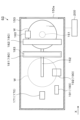
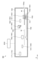
- the inspection device 63 has a housing 150.
- One side wall of the housing 150 is formed with a loading/unloading opening 150a for loading and unloading the wafer W into and from the housing 150.
- a wafer chuck 151 that holds a wafer W is provided inside the housing 150. That is, the housing 150 accommodates the wafer chuck 151.
- a guide rail 152 is provided on the bottom surface of the housing 150, extending from the front side (positive side of the X direction in FIG. 4) to the back side (negative side of the X direction in FIG. 4) of the housing 150.
- a drive unit 153 that rotates the wafer chuck 151 and is movable along the guide rail 152 is provided on the guide rail 152.
- the drive unit 153 has a drive source (not shown) such as a motor that generates a drive force for rotating the wafer chuck 151 and a drive force for moving the drive unit 153.
- the wafer W held by the wafer chuck 151 can be moved by the drive unit 153 between a first position near the loading/unloading port 150a, i.e., on the front side, and a second position near the peripheral imaging unit 190 described later, i.e., on the back side.
- This drive unit 153 constitutes at least a part of the movement mechanism that moves the wafer chuck 151.
- an aligner unit 160 is provided within the housing 150.
- the aligner unit 160 is provided at the front side within the housing 150.
- the aligner unit 160 has a light-projecting unit 161 at either the top or bottom, and a light-receiving unit 162 at the other.
- the light-projecting unit 161 includes, for example, an LED.
- the light-receiving unit 162 includes, for example, a PD (Photodiode).
- the aligner unit 160 is provided so that the peripheral portion of the wafer W held by the wafer chuck 151 and positioned at the first position described above can be sandwiched between the light-projecting unit 161 and the light-receiving unit 162.
- the control unit 200 detects the position of the notch formed on the peripheral edge of the wafer W. After the notch position is detected, the drive unit 153 rotates the wafer chuck 151, so that the wafer W, whose notch position has been detected, can be oriented in a predetermined direction.
- a surface imaging unit 170 Also provided within the housing 150 are a surface imaging unit 170 and a surface light source unit 180.
- the surface imaging unit 170 captures an image of the wafer W held by the wafer chuck 151 by receiving reflected light or scattered light from the wafer W.
- the surface imaging unit 170 has a camera 171.
- Camera 171 is provided, for example, at the upper end of the rear side (the negative X-direction side in FIG. 4) of housing 150, and has a lens (not shown) and an imaging device (not shown) such as a line sensor.
- the camera 171 serves as both a first imaging unit and a second imaging unit.
- the first imaging unit images the wafer W by receiving, as the first light, reflected light from the wafer W held on the wafer chuck 151 (specifically, reflected light from the surface of the wafer W), i.e., bright field light.
- the second imaging unit images the wafer W by receiving, as the second light, scattered light from the wafer W held on the wafer chuck 151 (specifically, scattered light from the surface of the wafer W), i.e., dark field light.
- the image captured by the camera 171 is output to the control unit 200 .
- the surface light source unit 180 emits light to the wafer W held by the wafer chuck 151.
- This surface light source unit 180 has a first light source unit 181 and a second light source unit 182.
- the first light source unit 181 is provided at the top at the center in the depth direction (X direction in the figure) within the housing 150, and a half mirror 183 is provided below the first light source unit 181.
- the half mirror 183 is provided in a position facing the camera 171, with the mirror surface tilted 45 degrees upward toward the camera 171 from a state in which the mirror surface faces vertically downward.
- the illumination from the first light source unit 181 passes through the half mirror 183 and is irradiated downward.
- the light that passes through the half mirror 183 is reflected by an object below the half mirror 183, is further reflected by the half mirror 183, and is received by the camera 171.
- the first light source unit 181 is bright field illumination, and the camera 171 can capture an image of an object in the area illuminated by the first light source unit 181. Therefore, when the wafer chuck 151 holding the wafer W moves along the guide rail 152, the camera 171 can capture an image of the surface of the wafer W passing through the irradiation area of the first light source unit 181.
- the second light source unit 182 is provided above the first light source unit 181 in the housing 150 at a position closer to the user (positive X-direction side in the figure). Illumination from the second light source unit 182 is directed diagonally downward.
- the light irradiation area by the second light source unit 182 and the light irradiation area by the first light source unit 181 are approximately the same. That is, for example, the second light source unit 182 illuminates the area below the half mirror 183.
- the light from the second light source unit 182 is scattered by an object below the half mirror 183, reflected by the half mirror 183, and received by the camera 171.
- the second light source unit 182 is a dark field illumination
- the camera 171 can capture an image of an object in the irradiation area by the second light source unit 182. Therefore, when the wafer chuck 151 holding the wafer W moves along the guide rail 152, the camera 171 can capture an image of the surface of the wafer W passing through the irradiation area of the second light source unit 182.
- a peripheral imaging unit 190 is provided within the housing 150 .
- the peripheral imaging unit 190 is provided, for example, on the rear side (the negative side in the X direction in FIG. 4) within the housing 150, and includes a camera 191, an illumination module 192, and a mirror member (not shown).
- Camera 191 has a lens (not shown) and an imaging element (not shown) such as a line sensor. The image captured by camera 191 is output to control unit 200.
- the lighting module 192 and the mirror member are configured so that, when the wafer W held by the wafer chuck 151 is in the second position, both the light emitted from the lighting module 192 and reflected by the peripheral portion of the surface of the wafer W, and the light emitted from the lighting module 192 and reflected by the side end surface of the wafer W are received by the camera 191.
- the camera 191 can capture images of both the peripheral portion of the surface of the wafer W and the side end surface of the wafer W.
- the peripheral imaging unit 190 captures an image in synchronization with the rotation of the wafer chuck 151 that holds the wafer W. This allows an image to be obtained that is substantially scanned in the circumferential direction of the wafer W for the entire peripheral portion of the wafer W, specifically, for the entire peripheral portion of the front surface of the wafer W and the entire side end surface of the wafer W.
- Fig. 6 is a flow chart for explaining the inspection of the wafer W by the inspection device 63, which is included in the above-mentioned wafer processing.
- a cassette C containing multiple wafers W is placed on a predetermined loading plate 21 of the cassette station 10. Then, under the control of the control unit 200, the wafers W are removed from the cassette C by the wafer transfer device 23 and transferred to, for example, the transfer device 52 in the third block G3 of the processing station 11.
- the wafer W is transported by the wafer transport device 70 to the heat treatment device 40 in the second block G2, where it is subjected to temperature adjustment processing.
- the wafer W is then transported by the wafer transport device 70 to, for example, the lower anti-reflection film forming device 31 in the first block G1, where a lower anti-reflection film is formed on the wafer W.
- the wafer W is then transported to the heat treatment device 40 for the lower layer film in the second block G2, where the lower layer film is subjected to heat processing.
- the wafer W is transferred to the resist coating device 32 in the first block G1, where a resist film is formed on the underlayer film of the wafer W.
- the wafer W is transferred to the heat treatment device 40 for PAB treatment in the second block G2, where the PAB treatment is performed.
- the wafer W is transferred to the upper anti-reflection film forming device 33 in the first block G1, where an upper anti-reflection film is formed on the wafer W.
- the wafer W is transferred to the heat treatment device 40 for the upper layer film in the second block G2, where the upper layer film is heated.
- the wafer W is transported by the wafer transport device 70 to the transfer device 52, and then by the shuttle transport device 80 to the transfer device 62 in the fourth block G4.
- the wafer W is then transported by the wafer transport device 100 in the interface station 13 to the inspection device 63, and loaded into the housing 150.
- the wafer W that has been brought into the housing 150 is placed on the wafer chuck 151 that has been moved to the front side within the housing 150 under the control of the control unit 200.
- the wafer W is carried into the housing 150 to the rear side. Specifically, the wafer W held by the wafer chuck 151 is moved along the guide rails 152 from the first position to the second position described above. At the first position, as described above, the position of the notch of the wafer W is detected, and the wafer W is oriented in a predetermined direction based on the detection result.
- the peripheral imaging unit 190 images the wafer W. Specifically, the peripheral imaging unit 190 images the peripheral portion of the surface of the wafer W and the side end surface of the wafer W.
- the wafer W is removed from the rear side of the housing 150 and moved to the front side of the housing 150.
- the wafer W is then removed from the housing 150 by the wafer transfer device 100 in the inspection device 63.
- the control unit 200 receives the image of the wafer W from the second position to the first position along the depth direction.
- the first light source unit 181 and the second light source unit 182 of the surface light source unit 180 are turned on.
- an image of the surface of the wafer W is captured by the camera 171 of the surface imaging unit 170.
- the imaging result by the surface imaging unit 170 is output to the control unit 200, and an image of the wafer W captured using dark field light (specifically, an image of the surface of the wafer W) is acquired by the control unit 200.
- the method for inspecting the wafer W according to the present embodiment inspects the wafer W based on an image of the wafer W captured by bright field light and an image of the wafer W captured by dark field light. Specifically, the method for inspecting the wafer W according to the present embodiment inspects the wafer W for defects based on the image of the wafer W captured by bright field light (hereinafter referred to as bright field inspection) and inspects the wafer W for defects based on the image of the wafer W captured by dark field light (hereinafter referred to as dark field inspection).
- the image of the wafer W captured by bright field light and the image of the wafer W captured by dark field light are acquired while the wafer W makes one round trip within the housing 150.
- the time required to acquire both images can be shortened compared to acquiring either an image of the wafer W captured by bright field light or an image of the wafer W captured by dark field light while the wafer W makes one round trip within the housing 150, and acquiring the other image while the wafer W makes another round trip within the housing 150. Therefore, according to this embodiment, it is possible to prevent the time required to acquire an image of the wafer W used for defect inspection of the wafer W from becoming long.
- control unit 200 performs both a defect inspection of the surface of the wafer W based on an image of the wafer W captured with bright field light, i.e., a bright field inspection, and a defect inspection of the surface of the wafer W based on an image of the wafer W captured with dark field light, i.e., a dark field inspection.
- the control unit 200 may estimate the cause of defects on the wafer W based on bright-field inspection and dark-field inspection.
- the control unit 200 estimates that the cause of the detected defect on the wafer W is poor coating, scratches, etc. Furthermore, if a defect is detected only by bright field inspection, it is assumed that the defect is present in the film, and therefore the control unit 200 presumes that foreign matter or bubbles in the coating liquid used to form the film are the cause of the detected defect on the wafer W.
- the thickness of the film on the wafer W can be determined, for example, based on a processing recipe stored in a memory unit (not shown). Information relating the defect detection results to their causes is stored in advance in the memory unit (not shown) and is referenced by the control unit 200 when estimating the cause of the defect.
- FIG. 7 is a vertical sectional view showing the outline of the configuration of an inspection device 63A serving as a board inspection device according to the second embodiment.
- the camera 171 of the front-side imaging unit 170 serves as both the first imaging unit and the second imaging unit described above.
- the front-side imaging unit 170A has a camera 301 as the first imaging unit and a camera 302 as the second imaging unit.
- the light irradiation area by the second light source unit 182 for dark field light coincides with the light irradiation area by the first light source unit 181 for bright field light.
- the light irradiation area by the second light source unit 182A for dark field light does not coincide with the light irradiation area by the first light source unit 181 for bright field light.
- the light irradiation area by the second light source unit 182A for dark field light is located in front of the light irradiation area by the first light source unit 181 for bright field light (the positive X-direction side in FIG. 7).
- the front surface imaging unit 170A captures an image of the wafer W under the control of the control unit 200.
- the wafer chuck 151 is moved in a first direction toward the rear of the housing 150 (the negative X direction in FIG. 4), while the bright field light from the wafer W held on the wafer chuck 151 is received by the front surface imaging unit 170A to capture an image of the wafer W.
- the wafer W which has been oriented in a predetermined direction at the first position, is moved along the depth direction to the second position while only the first light source unit 181A and the second light source unit 182A of the surface light source unit 180 are turned on.
- an image of the surface of the wafer W is captured by the camera 301 of the surface imaging unit 170A.
- the image captured by the camera 301 is output to the control unit 200, and an image of the wafer W captured using bright field light (specifically, an image of the surface of the wafer W) is acquired by the control unit 200.
- the wafer chuck 151 After imaging while moving toward the back of the housing 150 as described above, under the control of the control unit 200, the wafer chuck 151 is moved toward the front of the housing 150 (the positive X direction in FIG. 4), which is a second direction opposite to the first direction, while the dark field light from the wafer W held on the wafer chuck 151 is received by the front surface imaging unit 170A to image the wafer W.
- control unit 200 inspects the wafer W based on both images.
- ⁇ Modification 1 of the second embodiment> using the surface imaging unit 170A, one image of the wafer W is acquired using bright field light as the first light when the wafer W moves toward the back of the housing 150 (hereinafter abbreviated as "when moving toward the back"), and one image of the wafer W is acquired using dark field light as the second light when the wafer W moves toward the front of the housing 150 (hereinafter abbreviated as "when moving toward the front"), for a total of two images.
- a total of four images may be acquired by using the front surface imaging unit 170A to capture both an image of the wafer W captured by bright field light and an image of the wafer W captured by dark field light during each of the backward and forward movements. Then, the control unit 200 may inspect the wafer W based on the four captured images.
- the arrangement of the wafer W held by the wafer chuck 151 relative to the front surface imaging unit 170A does not differ between the time of movement in the rear direction and the time of movement in the front direction.
- the arrangement of the wafer W relative to the front surface imaging unit 170A may differ between the time of movement in the rear direction and the time of movement in the front direction, that is, the wafer W held by the wafer chuck 151 may be shifted relative to the front surface imaging unit 170A.
- the arrangement of the wafer W relative to the front surface imaging unit 170A is, for example, the orientation of the wafer W relative to the front surface imaging unit 170A. Specifically, the orientation of the wafer W relative to the front surface imaging unit 170A may be shifted by 45° between the time of movement in the rear direction and the time of movement in the front direction.
- the "positioning of the wafer W relative to the front surface imaging unit 170A" that is different when moving in the depth direction and when moving in the front direction may be the position of the wafer W in the perpendicular direction.
- the position of the wafer W held by the wafer chuck 151 in the perpendicular direction is shifted by half the pitch of the imaging elements of the line cameras that make up the cameras 301 and 302 when moving in the depth direction and when moving in the front direction.
- the above-mentioned "positioning of the wafer W relative to the front-surface imaging unit 170A" may be the angle of the top surface of the wafer chuck 151 relative to the horizontal plane, i.e., the angle of the surface of the wafer W relative to the horizontal plane.
- the position of the wafer W held by the wafer chuck 151 may be different when moving backward and forward.
- both the captured image of the wafer W using bright field light and the captured image of the wafer W using dark field light are acquired during each of the movement in the rearward direction and the movement in the forward direction.
- both the captured image of the wafer W using bright field light and the captured image of the wafer W using dark field light may be acquired only during either the movement in the rearward direction or the movement in the forward direction, and either one of the captured image of the wafer W using bright field light and the captured image of the wafer W using dark field light may be acquired during the other.
- a defect may be detected based on an image of the wafer W obtained by receiving one of the bright field light and dark field light obtained during the movement in the depth direction, i.e., a first defect detection is performed, and a defect may be detected based on an image of the wafer W obtained by the above one of the light receiving results obtained during the movement in the depth direction, i.e., a second defect detection is performed. Then, a defect detected by only one of the first defect detection and the second defect detection may be excluded from the defect detection result as a pseudo defect. In other words, when there are two images of the wafer W obtained by using the same illumination method, a defect detected based only on one of the images may be excluded from the defect detection result as a pseudo defect.
- both an image of the wafer W captured by bright field light and an image of the wafer W captured by dark field light are acquired only when moving in either the backward direction or the forward direction, and neither image needs to be acquired when moving in the other direction.
- the wafer W is moved back and forth only once in the housing 150.
- the wafer W may be moved back and forth again in the housing 150 according to the result of the inspection of the wafer W based on the captured image of the wafer W acquired in the first reciprocation, and an image of the wafer W may be acquired at that time, and the wafer W may be inspected again based on the acquired image.
- the arrangement of the wafer W with respect to the front surface imaging units 170 and 170A may be different between the movement in the back direction and the movement in the front direction.
- the position of the wafer W with respect to the front surface imaging units 170, 170A may be different between the first reciprocation and the second reciprocation.
- both defect detection based on an image of the wafer W captured with bright field light and defect detection based on an image of the wafer W captured with dark field light are performed. Then, if a defect is detected only in one of the two, only the bright field light or dark field light used for the captured image in which the defect was detected may be used for the third and subsequent wafers W.
- the first light is bright field light and the second light is dark field light, but the first light may be dark field light and the second light may be bright field light.
- the first light and the second light may be lights having different amounts of light received by the front-side imaging unit due to an aperture of the front-side imaging unit.
- defects that cannot be detected when only light with a small aperture and a large amount of light is used can be detected.
- the life of the light source can be extended compared to when only light with a large aperture and a small amount of light is used.
- an image of the wafer W may be acquired with light having a small aperture and a large amount of light when moving in the rearward direction, and a coarse defect inspection of the wafer W may be performed based on the acquired image, and only when a defect is detected, an image of the wafer W may be acquired with light having a large aperture and a small amount of light when moving in the forward direction. Then, a fine defect inspection of the wafer W may be performed based on the acquired image.
- An angle adjustment mechanism may be provided for adjusting the relative angle of light from the front surface light source unit with respect to the wafer W held on the wafer chuck 151.
- the angle adjustment mechanism may adjust the angle of the optical axis of the front surface light source unit, or may adjust the angle of the wafer mounting surface of the wafer chuck 151.
- the defect detection rate changes depending on the incident angle of the light with respect to the wafer W, so that the defect detection rate can be improved by providing the angle adjustment mechanism as described above.
- a substrate inspection device that inspects a substrate based on a captured image of the substrate, comprising: A holder for holding the substrate; a light source unit that emits light toward the substrate held by the holder; A moving mechanism that moves the holding unit; an imaging unit that images the substrate by receiving reflected light or scattered light from the substrate held by the holding unit; A control unit, The control unit is (A) moving the holding unit in a first direction while receiving a first light from the substrate held by the holding unit with the imaging unit to image the substrate; (B) then, while moving the holding portion in a second direction opposite to the first direction, the imaging portion receives a second light different from the first light from the substrate held by the holding portion, thereby imaging the substrate.
- the substrate inspection apparatus according to (1) wherein one of the first light and the second light is bright field light, and the other is dark field light.
- the substrate inspection apparatus according to (1), wherein the first light and the second light have different wavelength bands.
- the imaging unit has an aperture, The substrate inspection apparatus according to (1), wherein the first light and the second light are received by the imaging unit in amounts different from each other through the aperture.
- the light source unit includes a first light source unit for the first light and a second light source unit for the second light.
- the imaging unit includes a first imaging unit that receives the first light and a second imaging unit that receives the second light.
- the holding portion is moved while the first light and the second light from the substrate held by the holding portion are received by the first imaging portion and the second imaging portion, respectively, to image the substrate.
- the control unit of the substrate inspection apparatus described in (8) detects defects on the substrate based on an image of the substrate obtained during movement in the first direction in process (A) and an image of the substrate obtained during movement in the second direction in process (B).
- control unit (C) detecting defects on the substrate based on an image of the substrate captured as a result of receiving the first light; and (D) detecting defects on the substrate based on an image of the substrate captured by receiving the second light; and (E) a step of estimating a cause of the defect on the substrate based on the results of the steps (C) and (D).
- the control unit (F) detecting defects on the substrate based on an image of the substrate captured by receiving one of the first light and the second light obtained in the (A) step; (G) detecting defects on the substrate based on an image of the substrate obtained by the one light receiving result in the (B) step; (H) a step of excluding defects detected in only one of the steps (F) and (G) from the defect detection results.
- a substrate inspection device that inspects a substrate based on a captured image of the substrate, comprising: A holder for holding the substrate; a light source unit that emits light toward the substrate held by the holder; A moving mechanism that moves the holding unit; an imaging unit that images the substrate by receiving reflected light or scattered light from the substrate held by the holding unit; A control unit, The control unit is A substrate inspection device that performs a process of moving the holding portion in a predetermined direction, receiving a first light from the substrate held in the holding portion with the imaging portion to image the substrate, and receiving a second light, different from the first light, from the substrate held in the holding portion with the imaging portion to image the substrate.
- a method for inspecting a substrate based on an image of the substrate comprising: (a) moving a holder that holds the substrate in a first direction, receiving a first light from the substrate held by the holder with an imaging unit, and capturing an image of the substrate; (b) then, while moving the holding portion in a second direction opposite to the first direction, receiving a second light different from the first light from the substrate held by the holding portion with the imaging portion, and imaging the substrate.
- the imaging section includes a first imaging section that receives the first light and a second imaging section that receives the second light.
- the holding portion is moved while the first light and the second light from the substrate held by the holding portion are received by the first imaging portion and the second imaging portion, respectively, to image the substrate.
- One of the first light and the second light is bright field light, and the other is dark field light; (c) detecting defects on the substrate based on an image of the substrate captured as a result of receiving the first light; and (d) detecting defects on the substrate based on an image of the substrate captured as a result of receiving the second light; and (e) a step of estimating a cause of the defect on the substrate based on the results of the steps (C) and (D).
- a readable computer storage medium storing a program that operates on a computer of a control unit that controls a substrate inspection apparatus so as to cause the substrate inspection apparatus to execute a method for inspecting a substrate based on an image of the substrate, the program comprising: The method comprises: a step of receiving a first light from the substrate held by a holding unit with an imaging unit while moving the holding unit that holds the substrate in a first direction, and capturing an image of the substrate; Then, while moving the holding portion in a second direction opposite to the first direction, the imaging portion receives a second light different from the first light from the substrate held by the holding portion, and images the substrate.
Landscapes
- Physics & Mathematics (AREA)
- Health & Medical Sciences (AREA)
- Life Sciences & Earth Sciences (AREA)
- Chemical & Material Sciences (AREA)
- Analytical Chemistry (AREA)
- Biochemistry (AREA)
- General Health & Medical Sciences (AREA)
- General Physics & Mathematics (AREA)
- Immunology (AREA)
- Pathology (AREA)
- Investigating Materials By The Use Of Optical Means Adapted For Particular Applications (AREA)
- Testing Or Measuring Of Semiconductors Or The Like (AREA)
Abstract
基板の撮像画像に基づいて前記基板を検査する基板検査装置であって、前記基板を保持する保持部と、前記保持部に保持された前記基板に対して、光を出射する光源部と、前記保持部を移動させる移動機構と、前記保持部に保持された前記基板からの反射光または散乱光を受光することにより前記基板を撮像する撮像部と、制御部と、を備え、前記制御部は、(A)前記保持部を第1方向に移動させつつ、前記保持部に保持された前記基板からの第1光を、前記撮像部により受光させて、当該基板を撮像させる工程と、(B)その後、前記保持部を前記第1方向とは逆の第2方向に移動させつつ、前記保持部に保持された前記基板からの前記第1光とは異なる第2光を、前記撮像部により受光させて、当該基板を撮像させる工程と、を実行する。
Description
本開示は、基板検査装置、基板検査方法及び記憶媒体に関する。
特許文献1には、基板に所定の処理を施す複数の処理装置を備えた基板処理システムにおける、基板の検査方法が開示されている。この検査方法では、処理装置で処理される前の基板の表面を撮像して第1の基板画像が取得され、第1の基板画像から所定の特徴量が抽出される。また、それぞれ異なる範囲の特徴量に対応して設定された複数の検査レシピが記憶された記憶部から、第1の基板画像から抽出された特徴量に対応する検査レシピが選択される。そして、処理装置で処理された後の基板の表面を撮像して第2の基板画像が取得され、選択された検査レシピと第2の基板画像に基づいて、基板の欠陥の有無が判定される。
本開示にかかる技術は、基板の撮像画像に基づく欠陥検査における欠陥検出精度を向上させる。
本開示の一態様は、基板の撮像画像に基づいて前記基板を検査する基板検査装置であって、前記基板を保持する保持部と、前記保持部に保持された前記基板に対して、光を出射する光源部と、前記保持部を移動させる移動機構と、前記保持部に保持された前記基板からの反射光または散乱光を受光することにより前記基板を撮像する撮像部と、制御部と、を備え、前記制御部は、(A)前記保持部を第1方向に移動させつつ、前記保持部に保持された前記基板からの第1光を、前記撮像部により受光させて、当該基板を撮像させる工程と、(B)その後、前記保持部を前記第1方向とは逆の第2方向に移動させつつ、前記保持部に保持された前記基板からの前記第1光とは異なる第2光を、前記撮像部により受光させて、当該基板を撮像させる工程と、を実行する。
本開示によれば、基板の撮像画像に基づく欠陥検査における欠陥検出精度を向上させることができる。
半導体デバイス等の製造工程では、半導体ウェハ(以下、「ウェハ」という。)上にレジスト液を塗布してレジスト膜を形成するレジスト塗布処理、レジスト膜を露光する露光処理、露光されたレジスト膜を現像する現像処理等が順次行われ、ウェハ上にレジストパターンが形成される。
また、上述のようにレジストパターンを形成する際等に、各種処理後のウェハに対して欠陥検査が行われることがある。この欠陥検査では、例えば、膜表面の凹凸欠陥の有無や膜中の欠陥の有無等が検査される。近年では、この欠陥検査に、処理後の検査対象のウェハ(具体的にはその処理面すなわち表面)を撮像した撮像画像が用いられる場合がある(特許文献1参照)。
しかし、従来のウェハの撮像画像を用いてウェハに対し欠陥検査を行う方法では、欠陥検出精度の点で改善の余地がある。
しかし、従来のウェハの撮像画像を用いてウェハに対し欠陥検査を行う方法では、欠陥検出精度の点で改善の余地がある。
そこで、本開示にかかる技術は、基板の撮像画像に基づく欠陥検査における欠陥検出精度を向上させる。
以下、本実施形態にかかる基板検査装置及び基板検査方法を、図面を参照して説明する。なお、本明細書及び図面において、実質的に同一の機能構成を有する要素については、同一の符号を付することにより重複説明を省略する。
(第1実施形態)
<ウェハ処理システム>
図1は、第1実施形態にかかる基板検査装置を備えたウェハ処理システム1の構成の概略を示す平面図である。図2及び図3は、各々ウェハ処理システム1の正面側及び背面側の内部構成の概略を模式的に示す図である。なお、以下では、ウェハ処理システム1がウェハWに対して塗布現像処理を行う塗布現像処理システムである場合を例にして説明する。
<ウェハ処理システム>
図1は、第1実施形態にかかる基板検査装置を備えたウェハ処理システム1の構成の概略を示す平面図である。図2及び図3は、各々ウェハ処理システム1の正面側及び背面側の内部構成の概略を模式的に示す図である。なお、以下では、ウェハ処理システム1がウェハWに対して塗布現像処理を行う塗布現像処理システムである場合を例にして説明する。
ウェハ処理システム1は、例えば、ウェハWに対して塗布現像処理を行う塗布現像処理システムである。ウェハ処理システム1は、図1に示すように、複数枚のウェハWを収容したカセットCが搬入出されるカセットステーション10と、ウェハWに所定の処理を施す複数の各種処理装置を備えた処理ステーション11と、を有する。そして、ウェハ処理システム1は、カセットステーション10と、処理ステーション11と、処理ステーション11とは反対側に隣接する露光装置12との間でウェハWの受け渡しを行うインターフェイスステーション13と、を一体に接続した構成を有している。
カセットステーション10には、カセット載置台20が設けられている。カセット載置台20には、ウェハ処理システム1の外部に対してカセットCを搬入出する際に、カセットCを載置する載置板21が複数設けられている。
カセットステーション10には、X方向に延びる搬送路22上を移動自在なウェハ搬送装置23が設けられている。ウェハ搬送装置23は、上下方向及び鉛直軸周り(θ方向)にも移動自在であり、各載置板21上のカセットCと、後述する処理ステーション11の第3のブロックG3の受け渡し装置との間でウェハWを搬送できる。
処理ステーション11には、各種装置を備えた複数例えば4つのブロックG1、G2、G3、G4が設けられている。例えば処理ステーション11の正面側(図1のX方向負方向側)には、第1のブロックG1が設けられ、処理ステーション11の背面側(図1のX方向正方向側)には、第2のブロックG2が設けられている。また、処理ステーション11のカセットステーション10側(図1のY方向負方向側)には、第3のブロックG3が設けられ、処理ステーション11のインターフェイスステーション13側(図1のY方向正方向側)には、第4のブロックG4が設けられている。
第1のブロックG1には、図2に示すように、複数の液処理装置、例えば現像処理装置30、下部反射防止膜形成装置31、レジスト塗布装置32、上部反射防止膜形成装置33が下からこの順に配置されている。現像処理装置30は、ウェハWを現像処理するものであり、下部反射防止膜形成装置31は、ウェハWのレジスト膜の下層に反射防止膜(以下「下部反射防止膜」という)を形成するものである。レジスト塗布装置32は、ウェハWにレジスト液を塗布してレジスト膜を形成するものであり、上部反射防止膜形成装置33は、ウェハWのレジスト膜の上層に反射防止膜(以下「上部反射防止膜」という)を形成するものである。
例えば現像処理装置30、下部反射防止膜形成装置31、レジスト塗布装置32、上部反射防止膜形成装置33は、それぞれ水平方向に3つ並べて配置されている。なお、これら現像処理装置30、下部反射防止膜形成装置31、レジスト塗布装置32、上部反射防止膜形成装置33の数や配置は、任意に選択できる。
これら現像処理装置30、下部反射防止膜形成装置31、レジスト塗布装置32、上部反射防止膜形成装置33では、例えば、スピン塗布法により、予め定められた処理液がウェハW上に塗布される。スピン塗布法では、例えば塗布ノズルからウェハW上に処理液を吐出すると共に、ウェハWを回転させて、処理液をウェハWの表面に拡散させる。
第2のブロックG2には、図3に示すように、ウェハWの加熱や冷却といった熱処理を行う熱処理装置40が、上下方向と水平方向に並べて設けられており、その数や配置は、任意に選択できる。
第3のブロックG3には、複数の受け渡し装置50、51、52、53、54、55、56が下から順に設けられている。また、第4のブロックG4には、複数の受け渡し装置60、61、62と、基板検査装置としての検査装置63とが、下から順に設けられている。検査装置63の構成については後述する。
図1に示すように、第1のブロックG1~第4のブロックG4に囲まれた領域には、ウェハ搬送領域Dが形成されている。ウェハ搬送領域Dには、ウェハ搬送装置70が配置されている。
ウェハ搬送装置70は、例えばY方向、X方向、θ方向及び上下方向に移動自在な搬送アーム70aを有している。ウェハ搬送装置70は、ウェハ搬送領域D内を移動し、周囲の第1のブロックG1、第2のブロックG2、第3のブロックG3及び第4のブロックG4内の所定のユニットにウェハWを搬送できる。ウェハ搬送装置70は、例えば図3に示すように上下に複数台配置され、例えば各ブロックG1~G4の同程度の高さの所定の装置にウェハWを搬送できる。
また、ウェハ搬送領域Dには、第3のブロックG3と第4のブロックG4との間で直線的にウェハWを搬送するシャトル搬送装置80が設けられている。
シャトル搬送装置80は、例えば図3のY方向に直線的に移動自在になっている。シャトル搬送装置80は、ウェハWを支持した状態でY方向に移動し、第3のブロックG3の受け渡し装置52と第4のブロックG4の受け渡し装置62との間でウェハWを搬送できる。
図1に示すように、第3のブロックG3のX方向正方向側の隣には、ウェハ搬送装置90が設けられている。ウェハ搬送装置90は、例えばX方向、θ方向及び上下方向に移動自在な搬送アーム90aを有している。ウェハ搬送装置90は、ウェハWを支持した状態で上下に移動して、第3のブロックG3内の各受け渡し装置にウェハWを搬送できる。
インターフェイスステーション13には、ウェハ搬送装置100と受け渡し装置101が設けられている。ウェハ搬送装置100は、例えばY方向、θ方向及び上下方向に移動自在な搬送アーム100aを有している。ウェハ搬送装置100は、例えば搬送アーム100aにウェハWを支持して、第4のブロックG4内の各受け渡し装置、受け渡し装置101及び露光装置12との間でウェハWを搬送できる。
以上のウェハ処理システム1には、図1に示すように少なくとも1つの制御部200が設けられている。制御部200は、本開示において述べられる種々の工程をウェハ処理システム1に実行させるコンピュータ実行可能な命令を処理する。制御部200は、ここで述べられる種々の工程を実行するようにウェハ処理システム1の各要素を制御するように構成され得る。一実施形態において、制御部200の一部又は全てがウェハ処理システム1に含まれてもよい。制御部200は、処理部、記憶部及び通信インターフェースを含んでもよい。制御部200は、例えばコンピュータにより実現される。処理部は、記憶部から種々の制御動作を行うことを可能にするロジック又はルーチンを提供するプログラムを読み出し、読み出されたプログラムを実行することにより種々の制御動作を行うように構成され得る。このプログラムは、予め記憶部に格納されていてもよく、必要なときに、媒体を介して取得されてもよい。取得されたプログラムは、記憶部に格納され、処理部によって記憶部から読み出されて実行される。媒体は、コンピュータに読み取り可能な種々の記憶媒体であってもよく、通信インターフェースに接続されている通信回線であってもよい。記憶媒体は、一時的な記憶媒体であっても非一時的な記憶媒体Hであってもよい。処理部は、CPU(Central Processing Unit)であってもよく、1つ又は複数の回路であってもよい。記憶部は、RAM(Random Access Memory)、ROM(Read Only Memory)、HDD(Hard Disk Drive)、SSD(Solid State Drive)、又はこれらの組み合わせを含んでもよい。通信インターフェースは、LAN(Local Area Network)等の通信回線を介してウェハ処理システム1との間で通信してもよい。
<検査装置63>
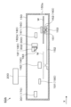
次に、上述した検査装置63の構成について説明する。図4及び図5はそれぞれ、検査装置63の構成の概略を示す横断面図及び縦断面図である。
次に、上述した検査装置63の構成について説明する。図4及び図5はそれぞれ、検査装置63の構成の概略を示す横断面図及び縦断面図である。
検査装置63は、図4及び図5に示すように、筐体150を有している。筐体150の一側壁には、当該筐体150に対するウェハWの搬入出を行うための搬入出口150aが形成されている。
また、筐体150内には、ウェハWを保持するウェハチャック151が設けられている。すなわち、筐体150は、ウェハチャック151を収容するものである。筐体150の底面には、筐体150内の手前側(図4中のX方向正方向側)から奥側(図4中のX方向負方向側)まで延伸するガイドレール152が設けられている。ガイドレール152上には、ウェハチャック151を回転させると共に、ガイドレール152に沿って移動自在な駆動部153が設けられている。駆動部153は、ウェハチャック151を回転させるための駆動力及び当該駆動部153の移動のための駆動力を発生するモータ等の駆動源(図示せず)を有する。ウェハチャック151に保持されているウェハWは、駆動部153により、搬入出口150a寄りすなわち手前側の第1の位置と、後述の周縁撮像ユニット190寄りすなわち奥側の第2の位置との間で移動可能である。この駆動部153は、ウェハチャック151を移動させる移動機構の少なくとも一部を構成する。
さらに、筐体150内には、アライナユニット160が設けられている。
アライナユニット160は、筐体150内における手前側に設けられている。また、アライナユニット160は、上部または下部のいずれか一方に投光部161を有し、他方に受光部162を有する。投光部161は例えばLEDを含む。受光部162は例えばPD(Photodiode)を含む。アライナユニット160は、ウェハチャック151に保持され上述の第1の位置に位置するウェハWの周縁部を投光部161と受光部162との間で挟みうるように設けられている。
例えば、第1の位置に位置するウェハWがウェハチャック151と共に駆動部153により回転されている間に、投光部161から受光部162に向けた光照射が行われ、受光部42での受光結果が制御部200に出力される。制御部200では、上記受光結果に基づいて、ウェハWの周縁部に形成されたノッチの位置が検出される。ノッチの位置の検出後、駆動部153によりウェハチャック151を回転させることにより、ノッチ位置検出済みのウェハWを、所定の向きとすることができる。
また、筐体150内には、表面用撮像部170と、表面用光源部180と、が設けられている。
表面用撮像部170は、ウェハチャック151に保持されたウェハWからの反射光または散乱光を受光することにより、当該ウェハWを撮像する。この表面用撮像部170は、カメラ171を有する。
カメラ171は、例えば、筐体150内の奥側(図4中のX方向負方向側)の端部における上方に設けられており、レンズ(図示せず)とラインセンサ等の撮像デバイス(図示せず)を有する。
本実施形態において、カメラ171は、第1撮像部及び第2撮像部を兼ねる。第1撮像部は、第1光としての、ウェハチャック151に保持されたウェハWからの反射光(具体的にはウェハWの表面からの反射光)すなわち明視野光を、受光することにより、ウェハWを撮像する。第2撮像部は、第2光としての、ウェハチャック151に保持されたウェハWからの散乱光(具体的にはウェハWの表面からの散乱光)すなわち暗視野光を、受光することにより、ウェハWを撮像する。
カメラ171で撮像された画像は、制御部200に出力される。
本実施形態において、カメラ171は、第1撮像部及び第2撮像部を兼ねる。第1撮像部は、第1光としての、ウェハチャック151に保持されたウェハWからの反射光(具体的にはウェハWの表面からの反射光)すなわち明視野光を、受光することにより、ウェハWを撮像する。第2撮像部は、第2光としての、ウェハチャック151に保持されたウェハWからの散乱光(具体的にはウェハWの表面からの散乱光)すなわち暗視野光を、受光することにより、ウェハWを撮像する。
カメラ171で撮像された画像は、制御部200に出力される。
表面用光源部180は、ウェハチャック151に保持されたウェハWに対して、光を出射する。この表面用光源部180は、第1光源部181と第2光源部182とを有する。
第1光源部181は、筐体150内の奥行き方向(図のX方向)中央における上方に設けられており、第1光源部181の下方には、ハーフミラー183が設けられている。ハーフミラー183は、カメラ171と対向する位置に、鏡面が鉛直下方を向いた状態からカメラ171の方向に向けて45度上方に傾斜した状態で設けられている。第1光源部181からの照明は、ハーフミラー183を通過して下方に向けて照らされる。また、ハーフミラー183を通過した光は、ハーフミラー183の下方にある物体によって反射され、ハーフミラー183でさらに反射して、カメラ171に受光される。すなわち、第1光源部181は、明視野照明であり、カメラ171は、第1光源部181による照射領域にある物体を撮像することができる。したがって、ウェハWを保持するウェハチャック151がガイドレール152に沿って移動する際に、カメラ171は、第1光源部181の照射領域を通過するウェハWの表面を撮像できる。
第2光源部182は、筐体150内の第1光源部181より手前側(図のX方向正方向側)の位置における上方に設けられている。第2光源部182からの照明は、斜め下方に向けて照らされる。また、第2光源部182による光照射領域と第1光源部181による光照射領域とは略一致する。すなわち、例えば、第2光源部182により、ハーフミラー183の下方が照らされる。また、第2光源部182からの光は、ハーフミラー183の下方にある物体によって散乱され、ハーフミラー183で反射して、カメラ171に受光される。すなわち、第2光源部182は、暗視野照明であり、カメラ171は、第2光源部182による照射領域にある物体を撮像することができる。したがって、ウェハWを保持するウェハチャック151がガイドレール152に沿って移動する際に、カメラ171は、第2光源部182の照射領域を通過するウェハWの表面を撮像できる。
さらに、筐体150内には、周縁撮像ユニット190が設けられている。
周縁撮像ユニット190は、例えば、筐体150内の奥側(図4中のX方向負方向側)に設けられており、カメラ191と、照明モジュール192と、ミラー部材(図示せず)とを含む。
周縁撮像ユニット190は、例えば、筐体150内の奥側(図4中のX方向負方向側)に設けられており、カメラ191と、照明モジュール192と、ミラー部材(図示せず)とを含む。
カメラ191は、レンズ(図示せず)とラインセンサ等の撮像素子(図示せず)を有する。カメラ191で撮像された画像は、制御部200に出力される。
照明モジュール192及びミラー部材は、ウェハチャック151に保持されたウェハWが第2の位置にある場合に、照明モジュール192から出射されウェハWの表面の周縁部で反射された光と、照明モジュール192から出射されウェハWの側端面で反射された光との双方がカメラ191に受光されるよう、構成されている。すなわち、ウェハチャック151に保持されたウェハWが第2の位置にある場合、カメラ191は、ウェハWの表面の周縁部とウェハWの側端面との双方を撮像できる。
例えば、ウェハWが第2の位置にある場合に、当該ウェハWを保持しているウェハチャック151の回転に同期させて、周縁撮像ユニット190による撮像が行われる。これにより、ウェハWの周縁部の全面について、具体的には、ウェハWの表面の周縁部の全面と、ウェハWの側端面の全面と、について、実質的にウェハWの周方向に走査した画像が得られる。
<ウェハ処理>
続いて、ウェハ処理システム1を用いて行われるウェハ処理の一例について説明する。図6は、上記ウェハ処理に含まれる、検査装置63によるウェハWの検査を説明するためのフローチャートである。
続いて、ウェハ処理システム1を用いて行われるウェハ処理の一例について説明する。図6は、上記ウェハ処理に含まれる、検査装置63によるウェハWの検査を説明するためのフローチャートである。
まず、複数のウェハWを収納したカセットCが、カセットステーション10の所定の載置板21に載置される。その後、制御部200の制御の下、ウェハWが、ウェハ搬送装置23によりカセットC内から取り出され、処理ステーション11の第3のブロックG3の例えば受け渡し装置52に搬送される。
次に、制御部200の制御の下、ウェハWが、ウェハ搬送装置70によって第2のブロックG2の熱処理装置40に搬送され、温度調節処理される。その後、ウェハWは、ウェハ搬送装置70によって例えば第1のブロックG1の下部反射防止膜形成装置31に搬送され、ウェハW上に下部反射防止膜が形成される。続いて、ウェハWが、第2のブロックG2の下層膜用の熱処理装置40に搬送され、下層膜の加熱処理が行われる。
その後、制御部200の制御の下、ウェハWが、第1のブロックG1のレジスト塗布装置32に搬送され、ウェハWの下層膜上にレジスト膜が形成される。続いて、ウェハWが、第2のブロックG2のPAB処理用の熱処理装置40に搬送され、PAB処理が行われる。
次に、制御部200の制御の下、ウェハWが、第1のブロックG1の上部反射防止膜形成装置33に搬送され、ウェハW上に上部反射防止膜が形成される。その後、ウェハWは第2のブロックG2の上層膜用の熱処理装置40に搬送され、上層膜の加熱処理が行われる。
次いで、制御部200の制御の下、ウェハWが、ウェハ搬送装置70によって受け渡し装置52に搬送され、シャトル搬送装置80によって第4のブロックG4の受け渡し装置62に搬送される。その後、ウェハWは、インターフェイスステーション13のウェハ搬送装置100によって検査装置63に搬送され、筐体150内に搬入される。
筐体150内に搬入されたウェハWは、制御部200の制御の下、筐体150内における手前側に移動してたウェハチャック151に載置される。
次いで、制御部200の制御の下、ウェハWは、筐体150内の奥側まで、搬入される。具体的には、ウェハチャック151に保持されたウェハWは、前述の第1の位置から第2の位置まで、ガイドレール152に沿って移動される。
第1の位置では、前述のように、ウェハWのノッチの位置が検出され、検出結果に基づいて、ウェハWが所定の向きとされる。
筐体150内への搬入動作が終わる第2の位置では、周縁撮像ユニット190によるウェハWの撮像が行われ、具体的には、周縁撮像ユニット190によるウェハWの表面の周縁部とウェハWの側端面の撮像が行われる。
第1の位置では、前述のように、ウェハWのノッチの位置が検出され、検出結果に基づいて、ウェハWが所定の向きとされる。
筐体150内への搬入動作が終わる第2の位置では、周縁撮像ユニット190によるウェハWの撮像が行われ、具体的には、周縁撮像ユニット190によるウェハWの表面の周縁部とウェハWの側端面の撮像が行われる。
その後、ウェハWは、制御部200の制御の下、筐体150内の奥側から搬出され、筐体150内の手前側まで移動される。そして、ウェハWは、ウェハ搬送装置100によって、検査装置63では、筐体150から搬出される。
また、検査装置63では、筐体150内にウェハWが位置する間に、制御部200の制御の下、表面用撮像部170によりウェハWが撮像される。
具体的には、制御部200の制御の下、図6に示すように、ウェハチャック151を第1方向である筐体150の奥方向(図4のX方向負方向)に移動させつつ、ウェハチャック151に保持されたウェハWからの明視野光を、表面用撮像部170により受光させて、ウェハWを撮像させる(ステップS1)。
より具体的には、筐体150内へのウェハWの搬入後、第1の位置で所定の向きとされたウェハWが、奥行き方向に沿って第2の位置まで移動される間、表面用光源部180の第1光源部181及び第2光源部182のうち前者のみが点灯される。また、第2の位置までの移動に同期して、表面用撮像部170のカメラ171によるウェハWの表面の撮像が行われる。表面用撮像部170による撮像結果は、制御部200に出力され、明視野光によるウェハWの撮像画像(具体的にはウェハWの表面の撮像画像)が制御部200により取得される。
上述の筐体150の奥方向に移動させつつの撮像後、制御部200の制御の下、ウェハチャック151を第1方向とは逆の第2方向である筐体150の手前方向(図4のX方向正方向)に移動させつつ、ウェハチャック151に保持されたウェハWからの暗視野光を、表面用撮像部170により受光させて、ウェハWを撮像させる(ステップS2)。
具体的には、ウェハWが、奥行き方向に沿って第2の位置から第1の位置まで移動される間、表面用光源部180の第1光源部181及び第2光源部182のうち後者のみが点灯される。また、第1の位置までの移動に同期して、表面用撮像部170のカメラ171によるウェハWの表面の撮像が行われる。表面用撮像部170による撮像結果は、制御部200に出力され、暗視野光によるウェハWの撮像画像(具体的にはウェハWの表面の撮像画像)が制御部200により取得される。
明視野光によるウェハWの撮像画像と、暗視野光によるウェハWの撮像画像とが取得されると、制御部200は、両撮像画像に基づいて、ウェハWを検査する(ステップS3)。具体的には、制御部200は、上記両撮像画像に基づいて、ウェハWの表面について欠陥検査を行う。より具体的には、制御部200は、明視野光によるウェハWの撮像画像に基づく当該ウェハWの表面の欠陥検査と、暗視野光によるウェハWの撮像画像に基づく当該ウェハWの表面の欠陥検査と、の両方を行う。明視野光によるウェハWの撮像画像に基づく欠陥検査は、予め取得された明視野光によるウェハWの基準画像を参照して行われる。例えば、基準画像からの画素値の変化量に基づいて欠陥が検出され、具体的には、基準画像からの画素値の変化量が閾値を超えた部分が欠陥として検出される。暗視野光によるウェハWの撮像画像に基づく欠陥検査についても同様である。
検査装置63の筐体150から搬出されたウェハWは、制御部200の制御の下、ウェハ搬送装置100によって露光装置12に搬送され、所定のパターンで露光処理される。次に、ウェハWは、ウェハ搬送装置100によって第4のブロックG4の受け渡し装置60に搬送される。その後、ウェハWは、ウェハ搬送装置70によって熱処理装置40に搬送され、PEB処理される。次に、ウェハWは、ウェハ搬送装置70によって現像処理装置30に搬送され、現像処理が行われる。
現像処理の終了後、ウェハWは、制御部200の制御の下、熱処理装置40に搬送され、ポストベーク処理される。次いで、ウェハWは、ウェハ搬送装置70により第3のブロックG3の受け渡し装置50に搬送される。その後、ウェハWは、カセットステーション10のウェハ搬送装置23によって所定の載置板21のカセットCに搬送され、一連のウェハ処理が完了する。上述のウェハ処理は、他のウェハWについても行われる。
<本実施形態の主な効果>
以上のように、本実施形態にかかるウェハWを検査する方法は、ウェハWを撮像した画像に基づいてウェハWを検査するものであり、
(a)ウェハチャック151を第1方向である筐体150の奥方向(図4のX方向負方向)に移動させつつ、ウェハチャック151に保持されたウェハWからの第1光としての明視野光を、表面用撮像部170により受光し、ウェハWを撮像する工程と、
(b)その後、ウェハチャック151を第1方向とは逆の第2方向である筐体150の手前方向(図4のX方向正方向)に移動させつつ、前記保持部に保持された前記基板からの前記第1光とは異なる第2光を、表面用撮像部170により受光させて、当該基板を撮像させる工程と、を含む。
すなわち、本実施形態にかかるウェハWを検査する方法は、明視野光によるウェハWの撮像画像及び暗視野光によるウェハWの撮像画像に基づいて、ウェハWを検査する。具体的には、本実施形態にかかるウェハWを検査する方法は、明視野光によるウェハWの撮像画像に基づく当該ウェハWの欠陥検査(以下、明視野検査という。)と、暗視野光によるウェハWの撮像画像に基づく当該ウェハWの欠陥検査(以下、暗視野検査という。)との両方を行う。
以上のように、本実施形態にかかるウェハWを検査する方法は、ウェハWを撮像した画像に基づいてウェハWを検査するものであり、
(a)ウェハチャック151を第1方向である筐体150の奥方向(図4のX方向負方向)に移動させつつ、ウェハチャック151に保持されたウェハWからの第1光としての明視野光を、表面用撮像部170により受光し、ウェハWを撮像する工程と、
(b)その後、ウェハチャック151を第1方向とは逆の第2方向である筐体150の手前方向(図4のX方向正方向)に移動させつつ、前記保持部に保持された前記基板からの前記第1光とは異なる第2光を、表面用撮像部170により受光させて、当該基板を撮像させる工程と、を含む。
すなわち、本実施形態にかかるウェハWを検査する方法は、明視野光によるウェハWの撮像画像及び暗視野光によるウェハWの撮像画像に基づいて、ウェハWを検査する。具体的には、本実施形態にかかるウェハWを検査する方法は、明視野光によるウェハWの撮像画像に基づく当該ウェハWの欠陥検査(以下、明視野検査という。)と、暗視野光によるウェハWの撮像画像に基づく当該ウェハWの欠陥検査(以下、暗視野検査という。)との両方を行う。
明視野検査と暗視野検査とでは、検出しやすい欠陥が異なる。
明視野検査では、撮像対象すなわち欠陥検出対象の光の反射率の変化を異常すなわち欠陥として検出するため、ウェハW上の膜表面の凹凸欠陥だけでなく、照明光の波長とウェハW上の膜の分光特性が合致すれば、上記膜中の欠陥も検出することができる。ただし、明視野検査では、照明光の波長が固定の場合、ウェハWの撮像画像が薄膜干渉の影響を受けるため、膜厚によっては、膜表面に凹凸欠陥があっても検出することは難しい。特に、ウェハW上の膜が厚いと、明視野検査では、欠陥検出精度が低下する。
一方、暗視野検査では、欠陥検出対象の表面からの散乱光を受光するため、ウェハW上の膜の厚さによらず、膜表面の凹凸結果は検出可能である。ただし、暗視野検査では、欠陥検出対象の表面からの散乱光を受光するため、膜中の欠陥は検出することが難しい。
明視野検査では、撮像対象すなわち欠陥検出対象の光の反射率の変化を異常すなわち欠陥として検出するため、ウェハW上の膜表面の凹凸欠陥だけでなく、照明光の波長とウェハW上の膜の分光特性が合致すれば、上記膜中の欠陥も検出することができる。ただし、明視野検査では、照明光の波長が固定の場合、ウェハWの撮像画像が薄膜干渉の影響を受けるため、膜厚によっては、膜表面に凹凸欠陥があっても検出することは難しい。特に、ウェハW上の膜が厚いと、明視野検査では、欠陥検出精度が低下する。
一方、暗視野検査では、欠陥検出対象の表面からの散乱光を受光するため、ウェハW上の膜の厚さによらず、膜表面の凹凸結果は検出可能である。ただし、暗視野検査では、欠陥検出対象の表面からの散乱光を受光するため、膜中の欠陥は検出することが難しい。
本実施形態では、このような明視野検査と暗視野検査の両方を行うため、いずれか一方を行う場合に比べて、ウェハWの撮像画像に基づく当該ウェハWの欠陥検査における欠陥検出精度を向上させることができる。具体的には、ウェハW上の膜の厚さによらず、ウェハW上の膜の表面の欠陥と、ウェハW上の膜中の欠陥との両方を検出することができる。
また、明視野光によるウェハWの撮像画像と暗視野光によるウェハWの撮像画像とを、ウェハWを筐体150内で一往復させる間に取得している。そのため、ウェハWを筐体150内で一往復させる間に、明視野光によるウェハWの撮像画像または暗視野光によるウェハWの撮像画像のいずれか一方を取得し、ウェハWを筐体150内でさらに一往復させる間に、他方を取得する場合に比べて、両撮像画像の取得に要する時間を短縮することができる。したがって、本実施形態によれば、ウェハWの欠陥検査に用いる当該ウェハWの撮像画像の取得に要する時間が長くなるのを抑制することができる。
<ウェハWの撮像画像に基づく当該ウェハWの検査>
次いで、明視野光によるウェハWの撮像画像と、暗視野光によるウェハWの撮像画像とに基づく、ウェハWの欠陥検査の一例について説明する。
次いで、明視野光によるウェハWの撮像画像と、暗視野光によるウェハWの撮像画像とに基づく、ウェハWの欠陥検査の一例について説明する。
前述のように、制御部200は、明視野光によるウェハWの撮像画像に基づく当該ウェハWの表面の欠陥検査すなわち明視野検査と、暗視野光によるウェハWの撮像画像に基づく当該ウェハWの表面の欠陥検査すなわち暗視野検査と、の両方を行う。
制御部200は、明視野検査及び暗視野検査に基づいて、ウェハW上の欠陥の要因を推定してもよい。
例えば、ウェハW上の膜が厚く且つ暗視野検査のみで欠陥が検出された場合、当該欠陥は膜表面に存在しているものと考えられるため、制御部200は、検出されたウェハW上の欠陥の要因を、塗布不良、スクラッチ等と推定する。
また、明視野検査のみで欠陥が検出された場合、当該欠陥は膜中に存在しているものと考えられるため、制御部200は、膜形成用の塗布液中の異物または泡が、検出されたウェハW上の欠陥の要因と推定する。
また、明視野検査のみで欠陥が検出された場合、当該欠陥は膜中に存在しているものと考えられるため、制御部200は、膜形成用の塗布液中の異物または泡が、検出されたウェハW上の欠陥の要因と推定する。
なお、ウェハW上の膜の厚さは、例えば、記憶部(図示せず)に記憶の処理レシピに基づいて判定可能である。また、欠陥検出結果とその要因とを関連付ける情報は、予め記憶部(図示せず)に記憶されており、欠陥の要因推定時に、制御部200に参照される。
(第2実施形態)
<検査装置63A>
次に、図7は、第2実施形態にかかる基板検査装置としての検査装置63Aの構成の概略を示す縦断面図である。
<検査装置63A>
次に、図7は、第2実施形態にかかる基板検査装置としての検査装置63Aの構成の概略を示す縦断面図である。
図4及び図5に示した第1実施形態にかかる検査装置63は、表面用撮像部170のカメラ171が、前述の第1撮像部及び第2撮像部を兼ねていた。それに対し、図7の第2実施形態にかかる検査装置63Aでは、表面用撮像部170Aが、第1撮像部としてのカメラ301と、第2撮像部としてのカメラ302と、を有する。
また、第1実施形態では、暗視野光用の第2光源部182による光照射領域と明視野光用の第1光源部181による光照射領域とが一致していた。それに対し、本実施形態では、暗視野光用の第2光源部182Aによる光照射領域が、明視野光用の第1光源部181による光照射領域が一致していない。具体的には、本実施形態では、例えば、暗視野光用の第2光源部182Aによる光照射領域は、明視野光用の第1光源部181による光照射領域の手前側(図7のX方向正方向側)に位置する。
検査装置63Aでも、第1実施形態にかかる検査装置63と同様、筐体150内にウェハWが位置する間に、制御部200の制御の下、表面用撮像部170AによりウェハWが撮像される。
具体的には、制御部200の制御の下、ウェハチャック151を第1方向である筐体150の奥方向(図4のX方向負方向)に移動させつつ、ウェハチャック151に保持されたウェハWからの明視野光を、表面用撮像部170Aにより受光させて、ウェハWを撮像させる。
より具体的には、筐体150内へのウェハWの搬入後、第1の位置で所定の向きとされたウェハWが、奥行き方向に沿って第2の位置まで移動される間、表面用光源部180の第1光源部181A及び第2光源部182Aのうち前者のみが点灯される。また、第2の位置までの移動に同期して、表面用撮像部170Aのカメラ301によるウェハWの表面の撮像が行われる。カメラ301による撮像結果は、制御部200に出力され、明視野光によるウェハWの撮像画像(具体的にはウェハWの表面の撮像画像)が制御部200により取得される。
上述の筐体150の奥方向に移動させつつの撮像後、制御部200の制御の下、ウェハチャック151を第1方向とは逆の第2方向である筐体150の手前方向(図4のX方向正方向)に移動させつつ、ウェハチャック151に保持されたウェハWからの暗視野光を、表面用撮像部170Aにより受光させて、ウェハWを撮像させる。
具体的には、ウェハWが、奥行き方向に沿って第2の位置から第1の位置まで移動される間、表面用光源部180Aの第1光源部181A及び第2光源部182Aのうち後者のみが点灯される。また、第1の位置までの移動に同期して、表面用撮像部170Aのカメラ302によるウェハWの表面の撮像が行われる。カメラ302による撮像結果は、制御部200に出力され、暗視野光によるウェハWの撮像画像(具体的にはウェハWの表面の撮像画像)が制御部200により取得される。
本実施形態においても、明視野光によるウェハWの撮像画像と、暗視野光によるウェハWの撮像画像とが取得されると、制御部200は、両撮像画像に基づいて、ウェハWを検査する。
<第2実施形態の変形例1>
以上の例では、表面用撮像部170Aを用いて、ウェハWの筐体150の奥方向への移動時(以下、「奥方向移動時」と省略。)に第1光としての明視野光によるウェハWの撮像画像が1枚取得され、ウェハWの筐体150の手前方向移動時(以下、「手前方向移動時」と省略。)に第2光としての暗視野光によるウェハWの撮像画像が1枚取得され、計2枚取得されていた。
これに代えて、表面用撮像部170Aを用いて、奥方向移動時及び手前方向移動時それぞれにおいて、明視野光によるウェハWの撮像画像と暗視野光によるウェハWの撮像画像との両方が取得され、計4枚取得されてもよい。そして、制御部200が、この4枚の撮像画像に基づいてウェハWが検査されてもよい。
以上の例では、表面用撮像部170Aを用いて、ウェハWの筐体150の奥方向への移動時(以下、「奥方向移動時」と省略。)に第1光としての明視野光によるウェハWの撮像画像が1枚取得され、ウェハWの筐体150の手前方向移動時(以下、「手前方向移動時」と省略。)に第2光としての暗視野光によるウェハWの撮像画像が1枚取得され、計2枚取得されていた。
これに代えて、表面用撮像部170Aを用いて、奥方向移動時及び手前方向移動時それぞれにおいて、明視野光によるウェハWの撮像画像と暗視野光によるウェハWの撮像画像との両方が取得され、計4枚取得されてもよい。そして、制御部200が、この4枚の撮像画像に基づいてウェハWが検査されてもよい。
また、以上の例では、表面用撮像部170Aを用いてウェハWの撮像画像が取得される際に、奥方向移動時と手前方向移動時とで、表面用撮像部170Aに対するウェハチャック151に保持されたウェハWの配置(以下、「表面用撮像部170Aに対するウェハWの配置」と省略。)が異なっていなかった。これに代えて、表面用撮像部170Aを用いてウェハWの撮像画像が取得される際に、奥方向移動時と手前方向移動時とで、表面用撮像部170Aに対するウェハWの配置が異なっていてもよく、すなわち、表面用撮像部170Aに対しウェハチャック151に保持されたウェハWがずらされていてもよい。表面用撮像部170Aに対するウェハWの配置とは、例えば、表面用撮像部170Aに対するウェハWの向きであり、具体的には、奥方向移動時と手前方向移動時とで、表面用撮像部170Aに対するウェハWの向きが45°ずれていてもよい。
これにより、ウェハW内において反射光または散乱光がカメラ301、302を構成するラインカメラの撮像素子間に到達してしまい受光されない部分を、奥方向移動時と手前方向移動時とで異ならせることができる。そのため、表面用撮像部170Aに対するウェハWの配置が互い異なる、奥方向移動時のウェハWの撮像画像と手前方向移動時のウェハWの撮像画像とに基づいて、ウェハWの検査を行うことにより、以下の効果がある。すなわち、奥方向移動時と手前方向移動時とで表面用撮像部170Aに対するウェハWの配置が異なっていない場合には欠陥の検出することができなかった部分についても、欠陥を検出することができる。
ウェハチャック151が、水平面内で奥行き方向と直交する方向に移動自在に構成されている場合は、奥方向移動時と手前方向移動時とで異ならせる「表面用撮像部170Aに対するウェハWの配置」は、ウェハWの上記直交する方向にかかる位置であってもよい。この場合、例えば、奥方向移動時と手前方向移動時とで、ウェハチャック151に保持されたウェハWの上記直交する方向にかかる位置が、カメラ301、302を構成するラインカメラの撮像素子のピッチの半分、ずらされる。
また、ウェハチャック151が、当該ウェハチャック151におけるウェハWが載置される上面の水平面に対する角度が調整自在に構成されている場合は、上記「表面用撮像部170Aに対するウェハWの配置」は、ウェハチャック151の上面の水平面に対する角度すなわちウェハWの表面の水平面に対する角度であってもよい。
なお、第1実施形態にかかる検査装置63を用いる場合も、表面用撮像部170を用いてウェハWの撮像画像が取得される際に、奥方向移動時と手前方向移動時とで、ウェハチャック151に保持されたウェハWの配置が異なっていてもよい。
<第2実施形態の変形例2>
上記変形例1では、奥方向移動時及び手前方向移動時それぞれにおいて、明視野光によるウェハWの撮像画像と暗視野光によるウェハWの撮像画像との両方が取得されていた。これに代えて、奥方向移動時または手前方向移動時のいずれか一方においてのみ、明視野光によるウェハWの撮像画像と暗視野光によるウェハWの撮像画像との両方が取得され、いずれか他方において、明視野光によるウェハWの撮像画像または暗視野光によるウェハWの撮像画像のいずれか1つが取得されてもよい。
上記変形例1では、奥方向移動時及び手前方向移動時それぞれにおいて、明視野光によるウェハWの撮像画像と暗視野光によるウェハWの撮像画像との両方が取得されていた。これに代えて、奥方向移動時または手前方向移動時のいずれか一方においてのみ、明視野光によるウェハWの撮像画像と暗視野光によるウェハWの撮像画像との両方が取得され、いずれか他方において、明視野光によるウェハWの撮像画像または暗視野光によるウェハWの撮像画像のいずれか1つが取得されてもよい。
また、奥方向移動時に得られた明視野光及び暗視野光のうちの一方の受光結果によるウェハWの撮像画像に基づいて欠陥が検出され、すなわち、第1欠陥検出が行われ、奥方向移動時に得られた上記一方の受光結果によるウェハWの撮像画像に基づいて欠陥が検出され、すなわち、第2欠陥検出が行われてもよい。そして、第1欠陥検出及び第2欠陥検出の一方のみで検出された欠陥が欠陥検出結果から疑似欠陥として除外されてもよい。すなわち、同じ照明方法によりウェハWを撮像した画像が2つある場合は、一方の画像に基づいてのみ検出された欠陥が欠陥検出結果から疑似欠陥として除外されてもよい。
<第2実施形態の変形例3>
また、奥方向移動時または手前方向移動時のいずれか一方においてのみ、明視野光によるウェハWの撮像画像と暗視野光によるウェハWの撮像画像との両方が取得され、いずれか他方では、いずれの撮像画像が取得されなくてもよい。
また、奥方向移動時または手前方向移動時のいずれか一方においてのみ、明視野光によるウェハWの撮像画像と暗視野光によるウェハWの撮像画像との両方が取得され、いずれか他方では、いずれの撮像画像が取得されなくてもよい。
<第1実施形態及び第2実施形態の変形例>
以上の例では、ウェハWを筐体150内で一往復のみさせていた。これに代えて、一往復目で取得されたウェハWの撮像画像に基づくウェハWの検査の結果に応じて、ウェハWを筐体150内で再度往復させ、その際、ウェハWの画像を取得させ、当該画像に基づいて、再度ウェハWの検査を行ってもよい。例えば、一往復目で、明視野光によるウェハWの撮像画像と暗視野光によるウェハWの撮像画像とのうち、一方に基づいてのみ欠陥が検出された場合、再度往復させる時には、明視野光と暗視野光のうち、欠陥が検出された撮像画像に用いられた方のみ、利用されてもよい。この場合、再度往復させる時における、奥方向への移動時及び手前方向移動時それぞれにおいて、ウェハWの撮像画像が取得されてもよい。また、再度往復させる時にウェハWの撮像画像を取得させる際に、奥方向移動時と、手前方向移動時とで、表面用撮像部170、170Aに対するウェハWの配置を異ならせてもよい。これに代えて、または、これに加えて、一往復目と、再度往復させる時とで、表面用撮像部170、170Aに対するウェハWの配置を異ならせてもよい。
以上の例では、ウェハWを筐体150内で一往復のみさせていた。これに代えて、一往復目で取得されたウェハWの撮像画像に基づくウェハWの検査の結果に応じて、ウェハWを筐体150内で再度往復させ、その際、ウェハWの画像を取得させ、当該画像に基づいて、再度ウェハWの検査を行ってもよい。例えば、一往復目で、明視野光によるウェハWの撮像画像と暗視野光によるウェハWの撮像画像とのうち、一方に基づいてのみ欠陥が検出された場合、再度往復させる時には、明視野光と暗視野光のうち、欠陥が検出された撮像画像に用いられた方のみ、利用されてもよい。この場合、再度往復させる時における、奥方向への移動時及び手前方向移動時それぞれにおいて、ウェハWの撮像画像が取得されてもよい。また、再度往復させる時にウェハWの撮像画像を取得させる際に、奥方向移動時と、手前方向移動時とで、表面用撮像部170、170Aに対するウェハWの配置を異ならせてもよい。これに代えて、または、これに加えて、一往復目と、再度往復させる時とで、表面用撮像部170、170Aに対するウェハWの配置を異ならせてもよい。
また、例えば、カセットCに収容されている複数枚(例えば25枚)のウェハWのうち、2枚目のウェハWに対し、明視野光によるウェハWの撮像画像に基づく欠陥検出と暗視野光によるウェハWの撮像画像とに基づく欠陥検出との両方が行われる。そして、一方でのみ欠陥が検出された場合、明視野光と暗視野光のうち、欠陥が検出された撮像画像に用いられた方のみ、3枚目以降のウェハWに利用されてもよい。
<第1光及び第2光の変形例>
以上の例では、第1光が明視野光、第2光が暗視野光であったが、第1光が暗視野光、第2光が明視野光であってもよい。
以上の例では、第1光が明視野光、第2光が暗視野光であったが、第1光が暗視野光、第2光が明視野光であってもよい。
また、第1光及び第2光は、暗視野光と明視野光の組み合わせに限られない。例えば、第1光及び第2光は、互いに波長帯が異なる光であってもよい。具体的には、第1光及び第2光の一方の波長帯は、他方の波長帯に全て含まれてもよく、すなわち、他方の波長帯の一部であってもよい。このような波長帯が異なる第1光及び第2光の両方を用いることにより、第1光及び第2光の一方のみを用いる場合では検出することができない欠陥を検出し得る。
また、第1光及び第2光は、表面用撮像部が有する絞りによって当該表面用撮像部に受光される光量が互いに異なる光であってもよい。このような、絞りによって表面用撮像部に受光される光量が互いに異なる第1光及び第2光の両方を用いることにより、絞り量が少なく光量が多い光のみを用いる場合には検出することができない欠陥を検出し得る。さらに、絞り量が多く光量が少ない光のみを用いる場合に比べて、光源の長寿命化を図ることができる。
なお、奥方向移動時に絞り量が少なく光量が多い光によりウェハWの撮像画像が取得され、当該撮像画像に基づいて粗いウェハWの欠陥検査が行われ、欠陥が検出された場合のみ、手前方向移動時に絞り量が多く光量が少ない光によりウェハWの撮像画像が取得されてもよい。そして、当該撮像画像に基づいて精細なウェハWの欠陥検査が行われてもよい。
また、この場合、第1光用の光源部と第2光用の光源部とを別に設けなくてもよく、第1光用と第2光用とで光源部を共通にすることができる。
なお、奥方向移動時に絞り量が少なく光量が多い光によりウェハWの撮像画像が取得され、当該撮像画像に基づいて粗いウェハWの欠陥検査が行われ、欠陥が検出された場合のみ、手前方向移動時に絞り量が多く光量が少ない光によりウェハWの撮像画像が取得されてもよい。そして、当該撮像画像に基づいて精細なウェハWの欠陥検査が行われてもよい。
また、この場合、第1光用の光源部と第2光用の光源部とを別に設けなくてもよく、第1光用と第2光用とで光源部を共通にすることができる。
<表面用光源部の他の例>
ウェハチャック151に保持されたウェハWに対する表面用光源部からの光の相対的な角度を調整するための角度調整機構が設けられてもよい。角度調整機構は、表面用光源部の光軸の角度を調整するものであってもよいし、ウェハチャック151のウェハ載置面の角度を調整するものであってもよい。表面用光源部から照射される暗視野光の場合、ウェハWに対する光の入射角度によって、欠陥検出率が変わるため、上述のような角度調整機構を設けることで、欠陥検出率の向上を図ることができる。
ウェハチャック151に保持されたウェハWに対する表面用光源部からの光の相対的な角度を調整するための角度調整機構が設けられてもよい。角度調整機構は、表面用光源部の光軸の角度を調整するものであってもよいし、ウェハチャック151のウェハ載置面の角度を調整するものであってもよい。表面用光源部から照射される暗視野光の場合、ウェハWに対する光の入射角度によって、欠陥検出率が変わるため、上述のような角度調整機構を設けることで、欠陥検出率の向上を図ることができる。
今回開示された実施形態はすべての点で例示であって制限的なものではないと考えられるべきである。上記の実施形態は、添付の請求の範囲及びその主旨を逸脱することなく、様々な形態で省略、置換、変更されてもよい。例えば、上記実施形態の構成要件は任意に組み合わせることができる。当該任意の組み合せからは、組み合わせにかかるそれぞれの構成要件についての作用及び効果が当然に得られるとともに、本明細書の記載から当業者には明らかな他の作用及び他の効果が得られる。
また、本明細書に記載された効果は、あくまで説明的または例示的なものであって限定的ではない。つまり、本開示に係る技術は、上記の効果とともに、又は、上記の効果に代えて、本明細書の記載から当業者には明らかな他の効果を奏しうる。
なお、以下のような構成例も本開示の技術的範囲に属する。
(1)基板の撮像画像に基づいて前記基板を検査する基板検査装置であって、
前記基板を保持する保持部と、
前記保持部に保持された前記基板に対して、光を出射する光源部と、
前記保持部を移動させる移動機構と、
前記保持部に保持された前記基板からの反射光または散乱光を受光することにより前記基板を撮像する撮像部と、
制御部と、を備え、
前記制御部は、
(A)前記保持部を第1方向に移動させつつ、前記保持部に保持された前記基板からの第1光を、前記撮像部により受光させて、当該基板を撮像させる工程と、
(B)その後、前記保持部を前記第1方向とは逆の第2方向に移動させつつ、前記保持部に保持された前記基板からの前記第1光とは異なる第2光を、前記撮像部により受光させて、当該基板を撮像させる工程と、を実行する、基板検査装置。
(2)前記第1光及び前記第2光の一方は、明視野光であり、他方は、暗視野光である、前記(1)に記載の基板検査装置。
(3)前記第1光及び前記第2光は、互いに波長帯が異なる、前記(1)に記載の基板検査装置。
(4)前記撮像部は絞りを有し、
前記第1光及び前記第2光は、前記絞りによって前記撮像部に受光される光量が互いに異なる、前記(1)に記載の基板検査装置。
(5)前記光源部は、前記第1光用の第1光源部と、前記第2光用の第2光源部とを、含む、前記(1)~(4)のいずれか1に記載の基板検査装置。
(6)前記撮像部は、前記第1光を受光する第1撮像部と、前記第2光を受光する第2撮像部と、を含む、前記(1)~(5)のいずれか1に記載の基板検査装置。
(7)前記(A)工程及び前記(B)工程の少なくともいずれか一方において、前記保持部を移動させつつ、前記保持部に保持された前記基板からの前記第1光及び前記第2光をそれぞれ前記第1撮像部及び前記第2撮像部により受光させて、当該基板を撮像させる、前記(6)に記載の基板検査装置。
(8)前記制御部は、前記(A)工程時と前記(B)工程時とで、前記撮像部に対する前記保持部に保持された前記基板の配置を異ならせる、前記(7)に記載の基板検査装置。
(9)前記制御部は、前記(A)工程における前記第1方向への移動時に得られた前記基板の撮像画像と、前記(B)工程における前記第2方向への移動時に得られた前記基板の撮像画像と、に基づいて、前記基板上の欠陥を検出する、前記(8)に記載の基板検査装置。
(10)前記制御部は、
(C)前記第1光の受光結果による前記基板の撮像画像に基づいて、前記基板上の欠陥を検出する工程と、
(D)前記第2光の受光結果による前記基板の撮像画像に基づいて、前記基板上の欠陥を検出する工程と、
(E)前記(C)工程及び前記(D)工程の結果に基づいて、前記基板上の欠陥の要因を推定する工程と、を実行する、前記(2)に記載の基板検査装置。
(11)前記制御部は、
(F)前記(A)工程で得られた前記第1光及び前記第2光のうちの一方の受光結果による前記基板の撮像画像に基づいて、前記基板上の欠陥を検出する工程と、
(G)前記(B)工程で得られた前記一方の受光結果による前記基板の撮像画像に基づいて、前記基板上の欠陥を検出する工程と、
(H)前記(F)工程と前記(G)工程の一方のみで検出された欠陥を欠陥検出結果から除外する工程と、を実行する、前記(7)~(9)のいずれか1に記載の基板検査装置。
(12)基板の撮像画像に基づいて前記基板を検査する基板検査装置であって、
前記基板を保持する保持部と、
前記保持部に保持された前記基板に対して、光を出射する光源部と、
前記保持部を移動させる移動機構と、
前記保持部に保持された前記基板からの反射光または散乱光を受光することにより前記基板を撮像する撮像部と、
制御部と、を備え、
前記制御部は、
前記保持部を所定の方向に移動させつつ、前記保持部に保持された前記基板からの第1光を前記撮像部により受光させて当該基板を撮像させ、前記保持部に保持された前記基板からの前記第1光とは異なる第2光を、前記撮像部により受光させて当該基板を撮像させる工程を実行する、基板検査装置。
(13)基板の撮像画像に基づいて前記基板を検査する方法であって、
(a)前記基板を保持する保持部を第1方向に移動させつつ、前記保持部に保持された前記基板からの第1光を、撮像部により受光し、当該基板を撮像する工程と、
(b)その後、前記保持部を前記第1方向とは逆の第2方向に移動させつつ、前記保持部に保持された前記基板からの前記第1光とは異なる第2光を、前記撮像部により受光し、当該基板を撮像する工程と、を含む、基板検査方法。
(14)前記撮像部は、前記第1光を受光する第1撮像部と、前記第2光を受光する第2撮像部と、を含む、前記(13)に記載の基板検査方法。
(15)前記(a)工程及び前記(b)工程の少なくともいずれか一方において、前記保持部を移動させつつ、前記保持部に保持された前記基板からの前記第1光及び前記第2光をそれぞれ前記第1撮像部及び前記第2撮像部により受光し、当該基板を撮像する、前記(14)に記載の基板検査方法。
(16)前記(a)工程時と前記(b)工程時とで、前記撮像部に対する前記保持部に保持された前記基板の配置が異なる、前記(15)に記載の基板検査方法。
(17)前記(a)工程における前記第1方向への移動時に得られた前記基板の撮像画像と、前記(b)工程における前記第2方向への移動時に得られた前記基板の撮像画像と、に基づいて、前記基板上の欠陥を検出する工程をさらに含む、前記(16)に記載の基板検査方法。
(18)前記第1光及び前記第2光の一方は、明視野光であり、他方は、暗視野光であり、
(c)前記第1光の受光結果による前記基板の撮像画像に基づいて、前記基板上の欠陥を検出する工程と、
(d)前記第2光の受光結果による前記基板の撮像画像に基づいて、前記基板上の欠陥を検出する工程と、
(e)前記(C)工程及び前記(D)工程の結果に基づいて、前記基板上の欠陥の要因を推定する工程と、をさらに含む、前記(13)~(17)のいずれか1に記載の基板検査方法。
(19)(f)前記(a)工程で得られた前記第1光及び前記第2光のうちの一方の受光結果による前記基板の撮像画像に基づいて、前記基板上の欠陥を検出する工程と、
(g)前記(b)工程で得られた前記一方の受光結果による前記基板の撮像画像に基づいて、前記基板上の欠陥を検出する工程と、
(h)前記(f)工程と前記(g)工程の一方のみで検出された欠陥を欠陥検出結果から除外する工程と、をさらに含む、前記(15)~(17)のいずれか1に記載の基板検査方法。
(20)基板の撮像画像に基づいて前記基板を検査する方法を基板検査装置によって実行させるように、当該基板検査装置を制御する制御部のコンピュータ上で動作するプログラムを格納した読み取り可能なコンピュータ記憶媒体であって、
前記方法は、
前記基板を保持する保持部を第1方向に移動させつつ、前記保持部に保持された前記基板からの第1光を、撮像部により受光し、当該基板を撮像する工程と、
その後、前記保持部を前記第1方向とは逆の第2方向に移動させつつ、前記保持部に保持された前記基板からの前記第1光とは異なる第2光を、前記撮像部により受光し、当該基板を撮像する工程と、を含む、コンピュータ記憶媒体。
(1)基板の撮像画像に基づいて前記基板を検査する基板検査装置であって、
前記基板を保持する保持部と、
前記保持部に保持された前記基板に対して、光を出射する光源部と、
前記保持部を移動させる移動機構と、
前記保持部に保持された前記基板からの反射光または散乱光を受光することにより前記基板を撮像する撮像部と、
制御部と、を備え、
前記制御部は、
(A)前記保持部を第1方向に移動させつつ、前記保持部に保持された前記基板からの第1光を、前記撮像部により受光させて、当該基板を撮像させる工程と、
(B)その後、前記保持部を前記第1方向とは逆の第2方向に移動させつつ、前記保持部に保持された前記基板からの前記第1光とは異なる第2光を、前記撮像部により受光させて、当該基板を撮像させる工程と、を実行する、基板検査装置。
(2)前記第1光及び前記第2光の一方は、明視野光であり、他方は、暗視野光である、前記(1)に記載の基板検査装置。
(3)前記第1光及び前記第2光は、互いに波長帯が異なる、前記(1)に記載の基板検査装置。
(4)前記撮像部は絞りを有し、
前記第1光及び前記第2光は、前記絞りによって前記撮像部に受光される光量が互いに異なる、前記(1)に記載の基板検査装置。
(5)前記光源部は、前記第1光用の第1光源部と、前記第2光用の第2光源部とを、含む、前記(1)~(4)のいずれか1に記載の基板検査装置。
(6)前記撮像部は、前記第1光を受光する第1撮像部と、前記第2光を受光する第2撮像部と、を含む、前記(1)~(5)のいずれか1に記載の基板検査装置。
(7)前記(A)工程及び前記(B)工程の少なくともいずれか一方において、前記保持部を移動させつつ、前記保持部に保持された前記基板からの前記第1光及び前記第2光をそれぞれ前記第1撮像部及び前記第2撮像部により受光させて、当該基板を撮像させる、前記(6)に記載の基板検査装置。
(8)前記制御部は、前記(A)工程時と前記(B)工程時とで、前記撮像部に対する前記保持部に保持された前記基板の配置を異ならせる、前記(7)に記載の基板検査装置。
(9)前記制御部は、前記(A)工程における前記第1方向への移動時に得られた前記基板の撮像画像と、前記(B)工程における前記第2方向への移動時に得られた前記基板の撮像画像と、に基づいて、前記基板上の欠陥を検出する、前記(8)に記載の基板検査装置。
(10)前記制御部は、
(C)前記第1光の受光結果による前記基板の撮像画像に基づいて、前記基板上の欠陥を検出する工程と、
(D)前記第2光の受光結果による前記基板の撮像画像に基づいて、前記基板上の欠陥を検出する工程と、
(E)前記(C)工程及び前記(D)工程の結果に基づいて、前記基板上の欠陥の要因を推定する工程と、を実行する、前記(2)に記載の基板検査装置。
(11)前記制御部は、
(F)前記(A)工程で得られた前記第1光及び前記第2光のうちの一方の受光結果による前記基板の撮像画像に基づいて、前記基板上の欠陥を検出する工程と、
(G)前記(B)工程で得られた前記一方の受光結果による前記基板の撮像画像に基づいて、前記基板上の欠陥を検出する工程と、
(H)前記(F)工程と前記(G)工程の一方のみで検出された欠陥を欠陥検出結果から除外する工程と、を実行する、前記(7)~(9)のいずれか1に記載の基板検査装置。
(12)基板の撮像画像に基づいて前記基板を検査する基板検査装置であって、
前記基板を保持する保持部と、
前記保持部に保持された前記基板に対して、光を出射する光源部と、
前記保持部を移動させる移動機構と、
前記保持部に保持された前記基板からの反射光または散乱光を受光することにより前記基板を撮像する撮像部と、
制御部と、を備え、
前記制御部は、
前記保持部を所定の方向に移動させつつ、前記保持部に保持された前記基板からの第1光を前記撮像部により受光させて当該基板を撮像させ、前記保持部に保持された前記基板からの前記第1光とは異なる第2光を、前記撮像部により受光させて当該基板を撮像させる工程を実行する、基板検査装置。
(13)基板の撮像画像に基づいて前記基板を検査する方法であって、
(a)前記基板を保持する保持部を第1方向に移動させつつ、前記保持部に保持された前記基板からの第1光を、撮像部により受光し、当該基板を撮像する工程と、
(b)その後、前記保持部を前記第1方向とは逆の第2方向に移動させつつ、前記保持部に保持された前記基板からの前記第1光とは異なる第2光を、前記撮像部により受光し、当該基板を撮像する工程と、を含む、基板検査方法。
(14)前記撮像部は、前記第1光を受光する第1撮像部と、前記第2光を受光する第2撮像部と、を含む、前記(13)に記載の基板検査方法。
(15)前記(a)工程及び前記(b)工程の少なくともいずれか一方において、前記保持部を移動させつつ、前記保持部に保持された前記基板からの前記第1光及び前記第2光をそれぞれ前記第1撮像部及び前記第2撮像部により受光し、当該基板を撮像する、前記(14)に記載の基板検査方法。
(16)前記(a)工程時と前記(b)工程時とで、前記撮像部に対する前記保持部に保持された前記基板の配置が異なる、前記(15)に記載の基板検査方法。
(17)前記(a)工程における前記第1方向への移動時に得られた前記基板の撮像画像と、前記(b)工程における前記第2方向への移動時に得られた前記基板の撮像画像と、に基づいて、前記基板上の欠陥を検出する工程をさらに含む、前記(16)に記載の基板検査方法。
(18)前記第1光及び前記第2光の一方は、明視野光であり、他方は、暗視野光であり、
(c)前記第1光の受光結果による前記基板の撮像画像に基づいて、前記基板上の欠陥を検出する工程と、
(d)前記第2光の受光結果による前記基板の撮像画像に基づいて、前記基板上の欠陥を検出する工程と、
(e)前記(C)工程及び前記(D)工程の結果に基づいて、前記基板上の欠陥の要因を推定する工程と、をさらに含む、前記(13)~(17)のいずれか1に記載の基板検査方法。
(19)(f)前記(a)工程で得られた前記第1光及び前記第2光のうちの一方の受光結果による前記基板の撮像画像に基づいて、前記基板上の欠陥を検出する工程と、
(g)前記(b)工程で得られた前記一方の受光結果による前記基板の撮像画像に基づいて、前記基板上の欠陥を検出する工程と、
(h)前記(f)工程と前記(g)工程の一方のみで検出された欠陥を欠陥検出結果から除外する工程と、をさらに含む、前記(15)~(17)のいずれか1に記載の基板検査方法。
(20)基板の撮像画像に基づいて前記基板を検査する方法を基板検査装置によって実行させるように、当該基板検査装置を制御する制御部のコンピュータ上で動作するプログラムを格納した読み取り可能なコンピュータ記憶媒体であって、
前記方法は、
前記基板を保持する保持部を第1方向に移動させつつ、前記保持部に保持された前記基板からの第1光を、撮像部により受光し、当該基板を撮像する工程と、
その後、前記保持部を前記第1方向とは逆の第2方向に移動させつつ、前記保持部に保持された前記基板からの前記第1光とは異なる第2光を、前記撮像部により受光し、当該基板を撮像する工程と、を含む、コンピュータ記憶媒体。
63、63A 検査装置
151 ウェハチャック
153 駆動部
170、170A 表面用撮像部
171 カメラ
180 表面用光源部
180、180A 表面用光源部
200 制御部
H 記憶媒体
W ウェハ
151 ウェハチャック
153 駆動部
170、170A 表面用撮像部
171 カメラ
180 表面用光源部
180、180A 表面用光源部
200 制御部
H 記憶媒体
W ウェハ
Claims (20)
- 基板の撮像画像に基づいて前記基板を検査する基板検査装置であって、
前記基板を保持する保持部と、
前記保持部に保持された前記基板に対して、光を出射する光源部と、
前記保持部を移動させる移動機構と、
前記保持部に保持された前記基板からの反射光または散乱光を受光することにより前記基板を撮像する撮像部と、
制御部と、を備え、
前記制御部は、
(A)前記保持部を第1方向に移動させつつ、前記保持部に保持された前記基板からの第1光を、前記撮像部により受光させて、当該基板を撮像させる工程と、
(B)その後、前記保持部を前記第1方向とは逆の第2方向に移動させつつ、前記保持部に保持された前記基板からの前記第1光とは異なる第2光を、前記撮像部により受光させて、当該基板を撮像させる工程と、を実行する、基板検査装置。 - 前記第1光及び前記第2光の一方は、明視野光であり、他方は、暗視野光である、請求項1に記載の基板検査装置。
- 前記第1光及び前記第2光は、互いに波長帯が異なる、請求項1に記載の基板検査装置。
- 前記撮像部は絞りを有し、
前記第1光及び前記第2光は、前記絞りによって前記撮像部に受光される光量が互いに異なる、請求項1に記載の基板検査装置。 - 前記光源部は、前記第1光用の第1光源部と、前記第2光用の第2光源部とを、含む、請求項1~4のいずれか1項に記載の基板検査装置。
- 前記撮像部は、前記第1光を受光する第1撮像部と、前記第2光を受光する第2撮像部と、を含む、請求項1~4のいずれか1項に記載の基板検査装置。
- 前記(A)工程及び前記(B)工程の少なくともいずれか一方において、前記保持部を移動させつつ、前記保持部に保持された前記基板からの前記第1光及び前記第2光をそれぞれ前記第1撮像部及び前記第2撮像部により受光させて、当該基板を撮像させる、請求項6に記載の基板検査装置。
- 前記制御部は、前記(A)工程時と前記(B)工程時とで、前記撮像部に対する前記保持部に保持された前記基板の配置を異ならせる、請求項7に記載の基板検査装置。
- 前記制御部は、前記(A)工程における前記第1方向への移動時に得られた前記基板の撮像画像と、前記(B)工程における前記第2方向への移動時に得られた前記基板の撮像画像と、に基づいて、前記基板上の欠陥を検出する、請求項8に記載の基板検査装置。
- 前記制御部は、
(C)前記第1光の受光結果による前記基板の撮像画像に基づいて、前記基板上の欠陥を検出する工程と、
(D)前記第2光の受光結果による前記基板の撮像画像に基づいて、前記基板上の欠陥を検出する工程と、
(E)前記(C)工程及び前記(D)工程の結果に基づいて、前記基板上の欠陥の要因を推定する工程と、を実行する、請求項2に記載の基板検査装置。 - 前記制御部は、
(F)前記(A)工程で得られた前記第1光及び前記第2光のうちの一方の受光結果による前記基板の撮像画像に基づいて、前記基板上の欠陥を検出する工程と、
(G)前記(B)工程で得られた前記一方の受光結果による前記基板の撮像画像に基づいて、前記基板上の欠陥を検出する工程と、
(H)前記(F)工程と前記(G)工程の一方のみで検出された欠陥を欠陥検出結果から除外する工程と、を実行する、請求項7に記載の基板検査装置。 - 基板の撮像画像に基づいて前記基板を検査する基板検査装置であって、
前記基板を保持する保持部と、
前記保持部に保持された前記基板に対して、光を出射する光源部と、
前記保持部を移動させる移動機構と、
前記保持部に保持された前記基板からの反射光または散乱光を受光することにより前記基板を撮像する撮像部と、
制御部と、を備え、
前記制御部は、
前記保持部を所定の方向に移動させつつ、前記保持部に保持された前記基板からの第1光を前記撮像部により受光させて当該基板を撮像させ、前記保持部に保持された前記基板からの前記第1光とは異なる第2光を、前記撮像部により受光させて当該基板を撮像させる工程を実行する、基板検査装置。 - 基板の撮像画像に基づいて前記基板を検査する方法であって、
(a)前記基板を保持する保持部を第1方向に移動させつつ、前記保持部に保持された前記基板からの第1光を、撮像部により受光し、当該基板を撮像する工程と、
(b)その後、前記保持部を前記第1方向とは逆の第2方向に移動させつつ、前記保持部に保持された前記基板からの前記第1光とは異なる第2光を、前記撮像部により受光し、当該基板を撮像する工程と、を含む、基板検査方法。 - 前記撮像部は、前記第1光を受光する第1撮像部と、前記第2光を受光する第2撮像部と、を含む、請求項13に記載の基板検査方法。
- 前記(a)工程及び前記(b)工程の少なくともいずれか一方において、前記保持部を移動させつつ、前記保持部に保持された前記基板からの前記第1光及び前記第2光をそれぞれ前記第1撮像部及び前記第2撮像部により受光し、当該基板を撮像する、請求項14に記載の基板検査方法。
- 前記(a)工程時と前記(b)工程時とで、前記撮像部に対する前記保持部に保持された前記基板の配置が異なる、請求項15に記載の基板検査方法。
- 前記(a)工程における前記第1方向への移動時に得られた前記基板の撮像画像と、前記(b)工程における前記第2方向への移動時に得られた前記基板の撮像画像と、に基づいて、前記基板上の欠陥を検出する工程をさらに含む、請求項16に記載の基板検査方法。
- 前記第1光及び前記第2光の一方は、明視野光であり、他方は、暗視野光であり、
(c)前記第1光の受光結果による前記基板の撮像画像に基づいて、前記基板上の欠陥を検出する工程と、
(d)前記第2光の受光結果による前記基板の撮像画像に基づいて、前記基板上の欠陥を検出する工程と、
(e)前記(C)工程及び前記(D)工程の結果に基づいて、前記基板上の欠陥の要因を推定する工程と、をさらに含む、請求項13~17のいずれか1項に記載の基板検査方法。 - (f)前記(a)工程で得られた前記第1光及び前記第2光のうちの一方の受光結果による前記基板の撮像画像に基づいて、前記基板上の欠陥を検出する工程と、
(g)前記(b)工程で得られた前記一方の受光結果による前記基板の撮像画像に基づいて、前記基板上の欠陥を検出する工程と、
(h)前記(f)工程と前記(g)工程の一方のみで検出された欠陥を欠陥検出結果から除外する工程と、をさらに含む、請求項15~17のいずれか1項に記載の基板検査方法。 - 基板の撮像画像に基づいて前記基板を検査する方法を基板検査装置によって実行させるように、当該基板検査装置を制御する制御部のコンピュータ上で動作するプログラムを格納した読み取り可能なコンピュータ記憶媒体であって、
前記方法は、
前記基板を保持する保持部を第1方向に移動させつつ、前記保持部に保持された前記基板からの第1光を、撮像部により受光し、当該基板を撮像する工程と、
その後、前記保持部を前記第1方向とは逆の第2方向に移動させつつ、前記保持部に保持された前記基板からの前記第1光とは異なる第2光を、前記撮像部により受光し、当該基板を撮像する工程と、を含む、コンピュータ記憶媒体。
Applications Claiming Priority (2)
| Application Number | Priority Date | Filing Date | Title |
|---|---|---|---|
| JP2023094658A JP2024176244A (ja) | 2023-06-08 | 2023-06-08 | 基板検査装置、基板検査方法及び記憶媒体 |
| JP2023-094658 | 2023-06-08 |
Publications (1)
| Publication Number | Publication Date |
|---|---|
| WO2024252981A1 true WO2024252981A1 (ja) | 2024-12-12 |
Family
ID=93795928
Family Applications (1)
| Application Number | Title | Priority Date | Filing Date |
|---|---|---|---|
| PCT/JP2024/019522 Ceased WO2024252981A1 (ja) | 2023-06-08 | 2024-05-28 | 基板検査装置、基板検査方法及び記憶媒体 |
Country Status (3)
| Country | Link |
|---|---|
| JP (1) | JP2024176244A (ja) |
| TW (1) | TW202524080A (ja) |
| WO (1) | WO2024252981A1 (ja) |
Citations (9)
| Publication number | Priority date | Publication date | Assignee | Title |
|---|---|---|---|---|
| JPS6242039A (ja) * | 1985-08-19 | 1987-02-24 | Toshiba Corp | 表面検査装置 |
| JP2005308615A (ja) * | 2004-04-23 | 2005-11-04 | Olympus Corp | 表面欠陥検査装置 |
| JP2007101239A (ja) * | 2005-09-30 | 2007-04-19 | Hitachi Chem Co Ltd | 外観検査装置及び外観検査方法 |
| JP2009080064A (ja) * | 2007-09-27 | 2009-04-16 | Nuflare Technology Inc | パターン検査装置及びパターン検査方法 |
| JP2010032265A (ja) * | 2008-07-25 | 2010-02-12 | Canon Inc | 異物検査装置、露光装置及びデバイス製造方法 |
| JP2012181135A (ja) * | 2011-03-02 | 2012-09-20 | Kobelco Kaken:Kk | 内部欠陥検査装置および内部欠陥検査方法 |
| KR20160068228A (ko) * | 2014-12-05 | 2016-06-15 | 세메스 주식회사 | 웨이퍼 결함 검사 장치 |
| JP2016528478A (ja) * | 2013-06-04 | 2016-09-15 | ケーエルエー−テンカー コーポレイション | 欠陥検出を強化するための最良の開口及びモードを発見するための装置及び方法 |
| JP2020190457A (ja) * | 2019-05-21 | 2020-11-26 | 株式会社昭和電気研究所 | ウエハ検査装置 |
-
2023
- 2023-06-08 JP JP2023094658A patent/JP2024176244A/ja active Pending
-
2024
- 2024-05-27 TW TW113119495A patent/TW202524080A/zh unknown
- 2024-05-28 WO PCT/JP2024/019522 patent/WO2024252981A1/ja not_active Ceased
Patent Citations (9)
| Publication number | Priority date | Publication date | Assignee | Title |
|---|---|---|---|---|
| JPS6242039A (ja) * | 1985-08-19 | 1987-02-24 | Toshiba Corp | 表面検査装置 |
| JP2005308615A (ja) * | 2004-04-23 | 2005-11-04 | Olympus Corp | 表面欠陥検査装置 |
| JP2007101239A (ja) * | 2005-09-30 | 2007-04-19 | Hitachi Chem Co Ltd | 外観検査装置及び外観検査方法 |
| JP2009080064A (ja) * | 2007-09-27 | 2009-04-16 | Nuflare Technology Inc | パターン検査装置及びパターン検査方法 |
| JP2010032265A (ja) * | 2008-07-25 | 2010-02-12 | Canon Inc | 異物検査装置、露光装置及びデバイス製造方法 |
| JP2012181135A (ja) * | 2011-03-02 | 2012-09-20 | Kobelco Kaken:Kk | 内部欠陥検査装置および内部欠陥検査方法 |
| JP2016528478A (ja) * | 2013-06-04 | 2016-09-15 | ケーエルエー−テンカー コーポレイション | 欠陥検出を強化するための最良の開口及びモードを発見するための装置及び方法 |
| KR20160068228A (ko) * | 2014-12-05 | 2016-06-15 | 세메스 주식회사 | 웨이퍼 결함 검사 장치 |
| JP2020190457A (ja) * | 2019-05-21 | 2020-11-26 | 株式会社昭和電気研究所 | ウエハ検査装置 |
Also Published As
| Publication number | Publication date |
|---|---|
| TW202524080A (zh) | 2025-06-16 |
| JP2024176244A (ja) | 2024-12-19 |
Similar Documents
| Publication | Publication Date | Title |
|---|---|---|
| US10460998B2 (en) | Method for inspecting substrate, substrate inspection apparatus, exposure system, and method for producing semiconductor device | |
| TWI487897B (zh) | A substrate processing apparatus, a substrate processing method, a program and a computer memory medium | |
| TWI676799B (zh) | 基板之檢查方法、基板處理系統及電腦記錄媒體 | |
| US10352875B2 (en) | Inspection apparatus, inspection method, exposure method, and method for manufacturing semiconductor device | |
| KR20170098695A (ko) | 기판 처리 방법, 기판 처리 장치 및 컴퓨터 판독 가능한 기록 매체 | |
| TWI800586B (zh) | 基板處理裝置及基板處理方法 | |
| CN109427609B (zh) | 半导体晶片在线检验的系统及方法 | |
| JPWO2012081587A1 (ja) | 検査方法、検査装置、露光管理方法、露光システムおよび半導体デバイス | |
| US20130100441A1 (en) | Optical inspection apparatus and edge inspection device | |
| US20040063232A1 (en) | Surface inspection method, surface inspection apparatus, and recording medium and data signal for providing surface inspection program | |
| JP7157580B2 (ja) | 基板検査方法及び基板検査装置 | |
| JP4385419B2 (ja) | 外観検査方法及び外観検査装置 | |
| JP7090005B2 (ja) | 基板処理装置及び検査方法 | |
| JP4914854B2 (ja) | 欠陥検査方法、プログラム及びコンピュータ記憶媒体 | |
| KR102749664B1 (ko) | 기판 처리 장치 및 검사 방법 | |
| TW202344832A (zh) | 基板檢查裝置,基板檢查方法及基板檢查程式 | |
| WO2024252981A1 (ja) | 基板検査装置、基板検査方法及び記憶媒体 | |
| JP5825268B2 (ja) | 基板検査装置 | |
| KR20230095989A (ko) | 휨양 추정 장치 및 휨양 추정 방법 | |
| JP2022015474A (ja) | 検査装置及び基板搬送方法 | |
| JP2020025118A (ja) | 基板処理方法、基板処理装置及びコンピュータ読み取り可能な記録媒体 | |
| JP2026069901A (ja) | 基板処理方法、及び、基板処理装置 | |
| JP2025109030A (ja) | 基板撮像装置、基板撮像方法、及び記憶媒体 | |
| TW202536549A (zh) | 描繪裝置以及描繪方法 | |
| JP2025030184A (ja) | 基板エッジ検出方法 |
Legal Events
| Date | Code | Title | Description |
|---|---|---|---|
| 121 | Ep: the epo has been informed by wipo that ep was designated in this application |
Ref document number: 24819212 Country of ref document: EP Kind code of ref document: A1 |
|
| NENP | Non-entry into the national phase |
Ref country code: DE |