WO2024253051A1 - Onduleur multiniveau - Google Patents
Onduleur multiniveau Download PDFInfo
- Publication number
- WO2024253051A1 WO2024253051A1 PCT/JP2024/020137 JP2024020137W WO2024253051A1 WO 2024253051 A1 WO2024253051 A1 WO 2024253051A1 JP 2024020137 W JP2024020137 W JP 2024020137W WO 2024253051 A1 WO2024253051 A1 WO 2024253051A1
- Authority
- WO
- WIPO (PCT)
- Prior art keywords
- switching element
- capacitor
- inverter
- switching
- gate drivers
- Prior art date
- Legal status (The legal status is an assumption and is not a legal conclusion. Google has not performed a legal analysis and makes no representation as to the accuracy of the status listed.)
- Ceased
Links
Images


Classifications
-
- H—ELECTRICITY
- H02—GENERATION; CONVERSION OR DISTRIBUTION OF ELECTRIC POWER
- H02M—APPARATUS FOR CONVERSION BETWEEN AC AND AC, BETWEEN AC AND DC, OR BETWEEN DC AND DC, AND FOR USE WITH MAINS OR SIMILAR POWER SUPPLY SYSTEMS; CONVERSION OF DC OR AC INPUT POWER INTO SURGE OUTPUT POWER; CONTROL OR REGULATION THEREOF
- H02M7/00—Conversion of AC power input into DC power output; Conversion of DC power input into AC power output
- H02M7/42—Conversion of DC power input into AC power output without possibility of reversal
- H02M7/44—Conversion of DC power input into AC power output without possibility of reversal by static converters
- H02M7/48—Conversion of DC power input into AC power output without possibility of reversal by static converters using discharge tubes with control electrode or semiconductor devices with control electrode
- H02M7/483—Converters with outputs that each can have more than two voltages levels
- H02M7/487—Neutral point clamped inverters
Definitions
- the present disclosure relates to a multilevel inverter, and more particularly to a multilevel inverter having a bootstrap circuit.
- Patent document 1 discloses a switching element drive circuit for a three-level neutral point clamped inverter.
- the neutral point clamped inverter disclosed in Patent Document 1 includes a series circuit of a first switching element, a second switching element, a third switching element, and a fourth switching element, a first clamp diode, a second clamp diode, and a series circuit of two smoothing capacitors (DC power supply section) that smoothes the DC voltage and generates its neutral point potential.
- the switching element drive circuit also includes a first gate drive circuit (first gate driver) for driving the first switching element, a second gate drive circuit (second gate driver) for driving the second switching element, a third gate drive circuit (third gate driver) for driving the third switching element, and a fourth gate drive circuit (fourth gate driver) for driving the fourth switching element.
- a switching signal is input to the first gate drive circuit, the second gate drive circuit, the third gate drive circuit, and the fourth gate drive circuit by a control circuit (control unit).
- the switching element drive circuit also includes a gate power supply (power supply section).
- a capacitor is connected in parallel to the first gate drive circuit.
- the capacitor is charged by the gate power supply via a diode.
- the gate drive power supply for the first switching element is the voltage charged in the capacitor.
- a voltage drop in a bootstrap circuit including a capacitor and a diode can be a problem.
- the objective of this disclosure is to provide a multilevel inverter that can suppress voltage drops in the bootstrap circuit.
- a multilevel inverter includes a DC power supply unit, a plurality of inverter circuits, and a control device.
- the DC power supply unit has a positive electrode, a negative electrode, and an intermediate potential point.
- the plurality of inverter circuits are connected between the positive electrode and the negative electrode of the DC power supply unit.
- the control device controls the plurality of inverter circuits.
- Each of the plurality of inverter circuits is a neutral point clamped inverter.
- Each of the plurality of inverter circuits includes a first switching element, a second switching element, a third switching element, and a fourth switching element, and a first diode, a second diode, a third diode, and a fourth diode.
- the first diode, the second diode, the third diode, and the fourth diode are connected in inverse parallel to the first switching element, the second switching element, the third switching element, and the fourth switching element, respectively.
- the control device includes a plurality of first gate drivers, a plurality of second gate drivers, a plurality of third gate drivers, a plurality of fourth gate drivers, a plurality of bootstrap circuits, a power supply unit, and a control unit.
- the first gate drivers drive the first switching element of each of the inverter circuits.
- the second gate drivers drive the second switching element of each of the inverter circuits.
- the third gate drivers drive the third switching element of each of the inverter circuits.
- the fourth gate drivers drive the fourth switching element of each of the inverter circuits.
- the bootstrap circuits correspond one-to-one to the first gate drivers. Each of the bootstrap circuits supplies a voltage to a corresponding first gate driver among the first gate drivers.
- the power supply unit supplies a voltage to the bootstrap circuits.
- the control unit controls the first gate drivers, the second gate drivers, the third gate drivers, and the fourth gate drivers.
- Each of the bootstrap circuits includes a capacitor and a diode connected in series to the capacitor. The capacitance of the capacitor included in each of the bootstrap circuits is 10 ⁇ F or more and 50 ⁇ F or less.
- the multilevel inverter disclosed herein has the effect of making it possible to suppress voltage drops in the bootstrap circuit.
- FIG. 1 is a circuit diagram of a system including a multilevel inverter according to a first embodiment.
- FIG. 2 is an explanatory diagram of a current path when the switching circuit in the multilevel inverter of the first embodiment is in a first switching state.
- FIG. 3 is an explanatory diagram of a discharge path and a charge path when the switching circuit in the multilevel inverter of the first embodiment is in a first switching state.
- FIG. 4 is an explanatory diagram of a current path when the switching circuit is in the second switching state in the multilevel inverter of the first embodiment.
- FIG. 5 is an explanatory diagram of a discharge path and a charge path when the switching circuit is in the second switching state in the multilevel inverter of the first embodiment.
- FIG. 6 is an explanatory diagram of a current path when the switching circuit in the multilevel inverter of the first embodiment is in the third switching state.
- FIG. 7 is an explanatory diagram of a discharge path and a charge path when the switching circuit in the multilevel inverter of the first embodiment is in the third switching state.
- FIG. 8 is an explanatory diagram of voltage command values for each phase in the multilevel inverter of the first embodiment.
- FIG. 9 is an explanatory diagram of a group of voltage vectors related to the multilevel inverter of the first embodiment.
- FIG. 10 is a more detailed illustration of a group of voltage vectors for the multilevel inverter of the first embodiment.
- FIG. 11 is a vector diagram for explaining the operation of the control unit in the multilevel inverter of the first embodiment.
- FIG. 12 is a diagram showing a time chart of the switching state of each phase of the multilevel inverter of the first embodiment.
- FIG. 13 is a diagram showing a time chart of the on/off states of the first to fourth switching elements of the multilevel inverter of the first embodiment.
- FIG. 14A is a timing chart showing the relationship between a control signal to a switching element and a current flowing through a control terminal of the switching element when the switching element is turned on.
- FIG. 14B is a timing chart showing the relationship between a control signal to a switching element and a current flowing through a control terminal of the switching element when the switching element is turned off.
- FIG. 15A is a characteristic diagram showing the carrier frequency dependence of the voltage change of a capacitor included in a bootstrap circuit.
- FIG. 15B is a characteristic diagram showing the capacitance dependency of the voltage change of the capacitor included in the bootstrap circuit.
- FIG. 16 is a graph showing the relationship between the minimum capacitance of the capacitor included in the bootstrap circuit, the carrier frequency, and the multi-level vector control (MLVC) ratio.
- FIG. 17 is a graph showing the relationship between the minimum capacitance of the capacitor included in the bootstrap circuit and the carrier frequency.
- FIG. 18 is a graph showing the relationship between the minimum capacitance of the capacitor included in the bootstrap circuit and the multilevel vector control ratio.
- FIG. 19A is an explanatory diagram of command voltage vectors and first voltage vectors related to a multilevel inverter according to a comparative example.
- FIG. 19B is an explanatory diagram of a command voltage vector, a zero vector, and a second voltage vector for the multilevel inverter of the comparative example.
- FIG. 20 is a diagram showing a time chart of the switching state of each phase when the inverter circuit of each phase is controlled by replacing the first voltage vector with a zero vector and a second voltage vector in a multilevel inverter of a comparative example.
- FIG. 21 is a diagram showing a time chart of the on/off states of the first to fourth switching elements when the inverter circuit is controlled by replacing the first voltage vector with a zero vector and a second voltage vector in a multilevel inverter of a comparative example.
- FIG. 22 is a circuit diagram of a system including a multilevel inverter according to the second embodiment.
- FIG. 23 is an explanatory diagram of a current path when the switching circuit is in the first switching state in the multilevel inverter of the second embodiment.
- FIG. 24 is an explanatory diagram of a discharge path when the switching circuit is in the first switching state in the multilevel inverter of the second embodiment.
- FIG. 25 is an explanatory diagram of a current path when the switching circuit is in the second switching state in the multilevel inverter of the second embodiment.
- FIG. 26 is an explanatory diagram of a discharge path when the switching circuit is in the second switching state in the multilevel inverter of the second embodiment.
- FIG. 27 is an explanatory diagram of a current path when the switching circuit in the multilevel inverter of the second embodiment is in the third switching state.
- FIG. 24 is an explanatory diagram of a discharge path when the switching circuit is in the first switching state in the multilevel inverter of the second embodiment.
- FIG. 25 is an explanatory diagram of a current path when the switching circuit is in the second switching state in the
- FIG. 28 is an explanatory diagram of a discharge path and a charge path when the switching circuit in the multilevel inverter of the second embodiment is in the third switching state.
- FIG. 29 is an explanatory diagram of a current path when the switching circuit is in the second switching state in the multilevel inverter of the second embodiment.
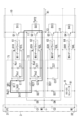
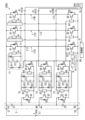
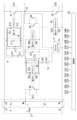
- FIG. 1 is a circuit diagram of a system including a multilevel inverter 100 according to a first embodiment.
- the multilevel inverter 100 includes a DC power supply unit 3, a plurality of (three in the example of FIG. 1) inverter circuits 1, and a control device 6.
- the DC power supply unit 3 has a positive electrode P1, a negative electrode N1, and an intermediate potential point M1.
- the plurality of inverter circuits 1 are connected between the positive electrode P1 and the negative electrode N1 of the DC power supply unit 3.
- the control device 6 controls the plurality of inverter circuits 1.
- the "intermediate potential point M1" is a point at an intermediate potential between the potential of the positive electrode P1 and the potential of the negative electrode N1 of the DC power supply unit 3.
- the multilevel inverter 100 is a three-level, three-phase inverter of a diode clamp type.
- each of the multiple inverter circuits 1 has an output terminal 41.
- an AC load RA1 is connected to multiple (three in the example of FIG. 1) output terminals 41.
- the AC load RA1 is, for example, a three-phase servo motor.
- one of the multiple inverter circuits 1 is an inverter circuit 1U that outputs a U-phase voltage, another is an inverter circuit 1V that outputs a V-phase voltage, and the remaining one is an inverter circuit 1W that outputs a W-phase voltage.
- Each of the multiple inverter circuits 1 has a switching circuit 10, a first diode D1, a second diode D2, a third diode D3, and a fourth diode D4.
- Each of the multiple inverter circuits 1 also has a first clamp diode D5 and a second clamp diode D6. In the multilevel inverter 100, the potential of the intermediate potential point M1 is clamped by the first clamp diode D5 and the second clamp diode D6 of each inverter circuit 1.
- the first switching element Q1, the second switching element Q2, the third switching element Q3, and the fourth switching element Q4 are connected in series from the positive pole P1 side to the negative pole N1 side of the DC power supply unit 3 in the order of the first switching element Q1, the second switching element Q2, the third switching element Q3, and the fourth switching element Q4.
- the first diode D1 is connected in anti-parallel to the first switching element Q1.
- the second diode D2 is connected in anti-parallel to the second switching element Q2.
- the third diode D3 is connected in anti-parallel to the third switching element Q3.
- the fourth diode D4 is connected in anti-parallel to the fourth switching element Q4.
- the first clamp diode D5 has a cathode connected to the first connection point 11 between the first switching element Q1 and the second switching element Q2, and an anode connected to the intermediate potential point M1.
- the second clamp diode D6 has an anode connected to the second connection point 12 between the third switching element Q3 and the fourth switching element Q4, and a cathode connected to the intermediate potential point M1.
- the control device 6 has a plurality of first gate drivers 61 (three in the example of FIG. 1), a plurality of second gate drivers 62 (three in the example of FIG. 1), a plurality of third gate drivers 63 (three in the example of FIG. 1), and a plurality of fourth gate drivers 64 (three in the example of FIG. 1).
- the control device 6 also has a plurality of bootstrap circuits 71 (three in the example of FIG. 1), a plurality of second bootstrap circuits 72 (three in the example of FIG. 1), a plurality of third bootstrap circuits 73 (three in the example of FIG. 1), a power supply unit 9, and a control unit 60.
- the multiple first gate drivers 61 drive the first switching element Q1 of each of the multiple inverter circuits 1.
- the multiple second gate drivers 62 drive the second switching element Q2 of each of the multiple inverter circuits 1.
- the multiple third gate drivers 63 drive the third switching element Q3 of each of the multiple inverter circuits 1.
- the multiple fourth gate drivers 64 drive the fourth switching element Q4 of each of the multiple inverter circuits 1.
- the multiple first bootstrap circuits 71 correspond one-to-one to the multiple first gate drivers 61. Each of the multiple first bootstrap circuits 71 supplies a voltage to the corresponding first gate driver 61.
- the multiple second bootstrap circuits 72 correspond one-to-one to the multiple second gate drivers 62. Each of the multiple second bootstrap circuits 72 supplies a voltage to the corresponding second gate driver 62.
- the multiple third bootstrap circuits 73 correspond one-to-one to the multiple third gate drivers 63. Each of the multiple third bootstrap circuits 73 supplies a voltage to the corresponding third gate driver 63.
- the power supply unit 9 supplies a voltage to the multiple fourth gate drivers 64.
- the control unit 60 controls a plurality of first gate drivers 61, a plurality of second gate drivers 62, a plurality of third gate drivers 63, and a plurality of fourth gate drivers 64.
- the DC power supply unit 3 has a first capacitor C1 and a second capacitor C2.
- the first capacitor C1 and the second capacitor C2 are connected in series.
- the DC power supply unit 3 further has a first DC terminal 31 connected to the positive pole P1 and a second DC terminal 32 connected to the negative pole N1.
- a first end of the first capacitor C1 is connected to the first DC terminal 31
- a second end of the first capacitor C1 is connected to the first end of the second capacitor C2, and a second end of the second capacitor C2 is connected to the second DC terminal 32.
- a connection point between the first capacitor C1 and the second capacitor C2 is an intermediate potential point M1.
- a DC voltage source E1 is connected between the first DC terminal 31 and the second DC terminal 32.
- the output voltage Vdc of the DC voltage source E1 is applied between the positive electrode P1 and the negative electrode N1 of the DC power supply unit 3.
- the capacitance of the second capacitor C2 is the same as the capacitance of the first capacitor C1.
- the capacitance of the second capacitor C2 is the same as the capacitance of the first capacitor C1
- the switching circuit 10 included in inverter circuit 1U may be referred to as switching circuit 10U
- the switching circuit 10 included in inverter circuit 1V may be referred to as switching circuit 10V
- the switching circuit 10 included in inverter circuit 1W may be referred to as switching circuit 10W
- the output terminal 41 included in inverter circuit 1U may be referred to as output terminal 41U
- the output terminal 41 included in inverter circuit 1V may be referred to as output terminal 41V
- the output terminal included in inverter circuit 1W may be referred to as output terminal 41W.
- the first switching element Q1, the second switching element Q2, the third switching element Q3, and the fourth switching element Q4 of each switching circuit 10 have a control terminal, a first main terminal, and a second main terminal.
- the first switching element Q1, the second switching element Q2, the third switching element Q3, and the fourth switching element Q4 of each switching circuit 10 are, for example, insulated gate bipolar transistors (IGBTs). Therefore, the control terminal, the first main terminal, and the second main terminal of each of the first switching element Q1, the second switching element Q2, the third switching element Q3, and the fourth switching element Q4 of each switching circuit 10 are the gate terminal, the collector terminal, and the emitter terminal, respectively.
- IGBTs insulated gate bipolar transistors
- the control terminal of the first switching element Q1 of each switching circuit 10 is connected to a corresponding first gate driver 61 of the multiple first gate drivers 61.
- the control terminal of the second switching element Q2 of each switching circuit 10 is connected to a corresponding second gate driver 62 of the multiple second gate drivers 62.
- the control terminal of the third switching element Q3 of each switching circuit 10 is connected to a corresponding third gate driver 63 of the multiple third gate drivers 63.
- the control terminal of the fourth switching element Q4 of each switching circuit 10 is connected to a corresponding fourth gate driver 64 of the multiple fourth gate drivers 64.
- the first main terminal of the first switching element Q1 is connected to the positive pole P1 of the DC power supply unit 3, and the second main terminal of the first switching element Q1 is connected to the first main terminal of the second switching element Q2. Also, in each switching circuit 10, the second main terminal of the second switching element Q2 is connected to the first main terminal of the third switching element Q3. Also, in each switching circuit 10, the second main terminal of the third switching element Q3 is connected to the first main terminal of the fourth switching element Q4, and the second main terminal of the fourth switching element Q4 is connected to the negative pole N1 of the DC power supply unit 3.
- the third connection point 13 between the second switching element Q2 and the third switching element Q3 in the switching circuit 10U is connected to the output terminal 41U.
- the third connection point 13 between the second switching element Q2 and the third switching element Q3 in the switching circuit 10V is connected to the output terminal 41V.
- the third connection point 13 between the second switching element Q2 and the third switching element Q3 in the switching circuit 10W is connected to the output terminal 41W.
- the third connection point 13 of the inverter circuit 1U is connected to, for example, the U phase of the AC load RA1 via the output terminal 41U.
- the third connection point 13 of the inverter circuit 1V is connected to, for example, the V phase of the AC load RA1 via the output terminal 41V.
- the third connection point 13 of the inverter circuit 1W is connected to, for example, the W phase of the AC load RA1 via the output terminal 41W.
- the anode of the first diode D1 is connected to the second main terminal (emitter terminal) of the first switching element Q1, and the cathode of the first diode D1 is connected to the first main terminal (collector terminal) of the first switching element Q1.
- the anode of the second diode D2 is connected to the second main terminal (emitter terminal) of the second switching element Q2, and the cathode of the second diode D2 is connected to the first main terminal (collector terminal) of the second switching element Q2.
- the anode of the third diode D3 is connected to the second main terminal (emitter terminal) of the third switching element Q3, and the cathode of the third diode D3 is connected to the first main terminal (collector terminal) of the third switching element Q3.
- the anode of the fourth diode D4 is connected to the second main terminal (emitter terminal) of the fourth switching element Q4, and the cathode of the fourth diode D4 is connected to the first main terminal (collector terminal) of the fourth switching element Q4.
- the first diode D1 may be replaced by a parasitic diode of the IGBT that constitutes the first switching element Q1.
- the second diode D2 may be replaced by a parasitic diode of the IGBT that constitutes the second switching element Q2.
- the third diode D3 may be replaced by a parasitic diode of the IGBT that constitutes the third switching element Q3.
- the fourth diode D4 may be replaced by a parasitic diode of the IGBT that constitutes the fourth switching element Q4.
- the cathode of the first clamp diode D5 is connected to the first connection point 11 between the first switching element Q1 and the second switching element Q2.
- the anode of the first clamp diode D5 is connected to the intermediate potential point M1 of the DC power supply unit 3.
- the intermediate potential point M1 is connected to ground, so the potential of the intermediate potential point M1 is 0V.
- the potential of the positive electrode P1 is Vdc/2
- the potential of the negative electrode N1 is -Vdc/2.
- the cathode of the second clamp diode D6 is connected to the intermediate potential point M1.
- the anode of the second clamp diode D6 is connected to the second connection point 12 between the third switching element Q3 and the fourth switching element Q4.
- the multiple first gate drivers 61 correspond one-to-one to the multiple first switching elements Q1. Each of the multiple first gate drivers 61 is connected to a control terminal of the corresponding first switching element Q1. Each of the multiple first gate drivers 61 drives the corresponding first switching element Q1.
- the multiple first gate drivers 61 are connected to the control unit 60.
- the control unit 60 outputs multiple first control signals S1 (see FIG. 2) that correspond one-to-one to the multiple first gate drivers 61.
- Each of the multiple first gate drivers 61 controls the on/off of the first switching element Q1 based on the given first control signal S1.
- the second gate drivers 62 correspond one-to-one to the second switching elements Q2. Each of the second gate drivers 62 is connected to a control terminal of the corresponding second switching element Q2. Each of the second gate drivers 62 drives the corresponding second switching element Q2.
- the second gate drivers 62 are connected to the control unit 60.
- the control unit 60 outputs second control signals S2 (see FIG. 2) that correspond one-to-one to the second gate drivers 62.
- Each of the second gate drivers 62 controls the on/off of the second switching element Q2 based on the second control signal S2 provided.
- the multiple third gate drivers 63 correspond one-to-one to the multiple third switching elements Q3. Each of the multiple third gate drivers 63 is connected to the control terminal of the corresponding third switching element Q3. Each of the multiple third gate drivers 63 drives the corresponding third switching element Q3.
- the multiple third gate drivers 63 are connected to the control unit 60.
- the control unit 60 outputs multiple third control signals S3 (see FIG. 2) that correspond one-to-one to the multiple third gate drivers 63.
- Each of the multiple third gate drivers 63 controls the on/off of the third switching element Q3 based on the provided third control signal S3.
- the multiple fourth gate drivers 64 correspond one-to-one to the multiple fourth switching elements Q4. Each of the multiple fourth gate drivers 64 is connected to the control terminal of the corresponding fourth switching element Q4. Each of the multiple fourth gate drivers 64 drives the corresponding fourth switching element Q4.
- the multiple fourth gate drivers 64 are connected to the control unit 60.
- the control unit 60 outputs multiple fourth control signals S4 (see FIG. 2) that correspond one-to-one to the multiple fourth gate drivers 64.
- Each of the multiple fourth gate drivers 64 controls the on/off of the fourth switching element Q4 based on the provided fourth control signal S4.
- the first bootstrap circuits 71 correspond one-to-one to the first gate drivers 61. Each of the first bootstrap circuits 71 supplies a voltage to a corresponding one of the first gate drivers 61. Each of the first bootstrap circuits 71 has a diode D17, a resistor R17, and a capacitor C17 (also called a boost capacitor C17). In each of the first bootstrap circuits 71, the anode of the diode D17 is connected to the positive terminal of the power supply unit 9 via the diodes D27 and D37, and the cathode of the diode D17 is connected to the first end of the capacitor C17 via the resistor R17.
- the first end of the capacitor C17 is connected to the high potential side power supply terminal 61H (see FIG. 3) of the first gate driver 61, and the second end of the capacitor C17 is connected to the low potential side power supply terminal 61L (see FIG. 3) of the first gate driver 61.
- the first bootstrap circuit 71 supplies the first gate driver 61 with a voltage required to turn on the first switching element Q1 in the first gate driver 61.
- Each of the first bootstrap circuits 71 further includes a Zener diode Z17 connected in parallel to the capacitor C17.
- the second bootstrap circuits 72 correspond one-to-one to the second gate drivers 62. Each of the second bootstrap circuits 72 supplies a voltage to a corresponding second gate driver 62 among the second gate drivers 62.
- Each of the second bootstrap circuits 72 has a diode D27, a resistor R27, and a capacitor C27 (also called a boost capacitor C27).
- the anode of the diode D27 is connected to the positive terminal of the power supply unit 9 via a diode D37, and the cathode of the diode D27 is connected to a first end of the capacitor C27 via a resistor R27.
- the first end of the capacitor C27 is connected to the high potential side power supply terminal 62H (see FIG.
- the second bootstrap circuit 72 supplies the second gate driver 62 with a voltage required to turn on the second switching element Q2 in the second gate driver 62.
- Each of the second bootstrap circuits 72 further includes a Zener diode Z27 connected in parallel to the capacitor C27.
- the third bootstrap circuits 73 correspond one-to-one to the third gate drivers 63. Each of the third bootstrap circuits 73 supplies a voltage to a corresponding third gate driver 63 among the third gate drivers 63.
- Each of the third bootstrap circuits 73 has a diode D37, a resistor R37, and a capacitor C37 (also called a boost capacitor C37).
- the anode of the diode D37 is connected to the positive terminal of the power supply unit 9, and the cathode of the diode D37 is connected to a first end of the capacitor C37 via the resistor R37.
- the first end of the capacitor C37 is connected to the high potential side power supply terminal 63H (see FIG.
- the third bootstrap circuit 73 supplies the third gate driver 63 with a voltage required to turn on the third switching element Q3 in the third gate driver 63.
- Each of the multiple third bootstrap circuits 73 further includes a Zener diode Z37 connected in parallel to the capacitor C37.
- the power supply unit 9 supplies voltage to the multiple (three) first bootstrap circuits 71, the multiple (three) second bootstrap circuits 72, the multiple (three) third bootstrap circuits 73, and the multiple (three) fourth gate drivers 64.
- the power supply unit 9 is, for example, a DC power supply including an isolated DC-DC converter 91.
- the positive terminal of the power supply unit 9 is connected to the high potential power supply terminal 64H (see FIG. 3) of each of the multiple fourth gate drivers 64, and the negative terminal of the power supply unit 9 is connected to the low potential power supply terminal 64L (see FIG. 3) of each of the multiple fourth gate drivers 64.
- the control unit 60 controls a plurality of first gate drivers 61, a plurality of second gate drivers 62, a plurality of third gate drivers 63, and a plurality of fourth gate drivers 64.
- the control unit 60 controls a plurality of first switching elements Q1, a plurality of second switching elements Q2, a plurality of third switching elements Q3, and a plurality of fourth switching elements Q4.
- the execution subject of the control unit 60 includes a computer system.
- the computer system has one or more computers.
- the computer system is mainly composed of a processor and a memory as hardware.
- the processor executes a program recorded in the memory of the computer system, thereby realizing the function of the control unit 60 as the execution subject in this disclosure.
- the program may be pre-recorded in the memory of the computer system, or may be provided through an electric communication line, or may be recorded and provided on a non-transitory recording medium such as a memory card, an optical disk, or a hard disk drive (magnetic disk) that can be read by the computer system.
- the processor of the computer system is composed of one or more electronic circuits including a semiconductor integrated circuit (IC) or a large-scale integrated circuit (LSI).
- the multiple electronic circuits may be integrated into one chip, or may be distributed across multiple chips.
- the multiple chips may be integrated into one device, or may be distributed across multiple devices.
- the control unit 60 outputs a plurality (three) of first control signals S1 (see FIG. 2) for controlling a plurality (three) of first switching elements Q1, a plurality (three) of second control signals S2 (see FIG. 2) for controlling a plurality (three) of second switching elements Q2, a plurality (three) of third control signals S3 (see FIG. 2) for controlling a plurality (three) of third switching elements Q3, and a plurality (three) of fourth control signals S4 (see FIG. 2) for controlling a plurality (three) of fourth switching elements Q4.
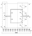
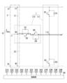
- FIG. 2 shows only one inverter circuit 1 of the three inverter circuits 1 (see FIG. 1), and the remaining two inverter circuits 1 are not shown.
- the first gate drivers 61, the second gate drivers 62, the third gate drivers 63, the fourth gate drivers 64, the first bootstrap circuits 71, the second bootstrap circuits 72, the third bootstrap circuits 73, and the power supply unit 9 shown in FIG. 1 are omitted.
- FIG. 3 only one inverter circuit 1 of the three inverter circuits 1 (see FIG. 1) is shown, and the remaining two inverter circuits 1 are omitted.
- the two first gate drivers 61, the two second gate drivers 62, the two third gate drivers 63, the two fourth gate drivers 64, the two first bootstrap circuits 71, the two second bootstrap circuits 72, and the two third bootstrap circuits 73 shown in FIG. 1 are omitted.
- the three first control signals S1 include a first control signal S1U that controls the first switching element Q1 of the switching circuit 10U, a first control signal S1V that controls the first switching element Q1 of the switching circuit 10V, and a first control signal S1W that controls the first switching element Q1 of the switching circuit 10W.
- the three second control signals S2 include a second control signal S2U that controls the second switching element Q2 of the switching circuit 10U, a second control signal S2V that controls the second switching element Q2 of the switching circuit 10V, and a second control signal S2W that controls the second switching element Q2 of the switching circuit 10W.
- the three third control signals S3 include a third control signal S3U that controls the third switching element Q3 of the switching circuit 10U, a third control signal S3V that controls the third switching element Q3 of the switching circuit 10V, and a third control signal S3W that controls the third switching element Q3 of the switching circuit 10W.
- the three fourth control signals S4 include a fourth control signal S4U that controls the fourth switching element Q4 of the switching circuit 10U, a fourth control signal S4V that controls the fourth switching element Q4 of the switching circuit 10V, and a fourth control signal S4W that controls the fourth switching element Q4 of the switching circuit 10W.
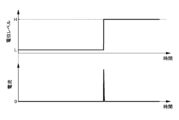
- Each of the multiple first control signals S1, multiple second control signals S2, multiple third control signals S3, and multiple fourth control signals S4 is, for example, a signal whose potential level changes between a first potential level (hereinafter also referred to as a low level) and a second potential level (hereinafter also referred to as a high level) that is higher than the first potential level.
- the first potential level is, for example, 0V
- the second potential level is a potential level greater than the gate threshold voltage of the IGBT. That is, for each of the multiple control signals (multiple first control signals S1, multiple second control signals S2, multiple third control signals S3, and multiple fourth control signals S4), the first potential level is a potential level for turning off the switching element corresponding to that control signal, and the second potential level is a potential level for turning on the switching element corresponding to that control signal.
- Each of the multiple first switching elements Q1 is turned on when the corresponding first control signal S1 is at a high level, and turned off when it is at a low level.
- Each of the multiple second switching elements Q2 is turned on when the corresponding second control signal S2 is at a high level, and turned off when it is at a low level.
- Each of the multiple third switching elements Q3 is turned on when the corresponding third control signal S3 is at a high level, and turned off when it is at a low level.
- Each of the multiple fourth switching elements Q4 is turned on when the corresponding fourth control signal S4 is at a high level, and turned off when it is at a low level.
- each of the multiple inverter circuits 1 is controlled to a first switching state, a second switching state, or a third switching state. That is, in the multilevel inverter 100, the switching state of the switching circuit 10 in each of the three inverter circuits 1U, 1V, and 1W is controlled to one of a first switching state, a second switching state, and a third switching state.
- the first switching state, the second switching state, and the third switching state have different combinations of on/off states of the first to fourth switching elements Q1 to Q4.
- the output voltage in the first switching state, the output voltage in the second switching state, and the output voltage in the third switching state are different from each other.
- the potential level of the output voltage changes in three levels depending on the state of the first to fourth switching elements Q1 to Q4.
- the output voltage of the U-phase inverter circuit 1U, the output voltage of the V-phase inverter circuit 1V, and the output voltage of the W-phase inverter circuit 1W are in different phases from each other.
- the first switching state is a combination in which both the first switching element Q1 and the second switching element Q2 are in the on state, and both the third switching element Q3 and the fourth switching element Q4 are in the off state.
- each of the multiple inverter circuits 1 can output an output voltage at the potential level of the positive electrode P1 of the DC power supply unit 3.
- each of the multiple inverter circuits 1 has the potential of the third connection point 13 at the potential level of the positive electrode P1 of the DC power supply unit 3 (e.g., Vdc/2).
- the second switching state is a combination in which both the first switching element Q1 and the fourth switching element Q4 are in the off state, and both the second switching element Q2 and the third switching element Q3 are in the on state.
- each of the multiple inverter circuits 1 can output an output voltage at the potential level of the intermediate potential point M1 of the DC power supply unit 3.
- the potential of the third connection point 13 becomes the potential level of the intermediate potential point M1 (e.g., 0).
- the third switching state is a combination in which both the first switching element Q1 and the second switching element Q2 are in the off state, and both the third switching element Q3 and the fourth switching element Q4 are in the on state.
- each of the multiple inverter circuits 1 can output an output voltage at the potential level of the negative electrode N1 of the DC power supply unit 3.
- each of the multiple inverter circuits 1 has the potential of the third connection point 13 at the potential level of the negative electrode N1 of the DC power supply unit 3 (for example, -Vdc/2).
- FIG 2 is an explanatory diagram of the current path when the switching circuit 10 is in the first switching state in the multilevel inverter 100 of embodiment 1.
- a current I1 flows through the path from the positive electrode P1 of the DC power supply unit 3 - the first switching element Q1 - the second switching element Q2 - the third connection point 13 - the output terminal 41, and the voltage value of the output voltage to the AC load RA1 (see Figure 1) becomes approximately Vdc/2.
- the switching circuit 10 of the inverter circuit 1 when the switching circuit 10 of the inverter circuit 1 is in the first switching state, the voltage required for the first gate driver 61 to turn on the first switching element Q1 is supplied from the capacitor C17 of the first bootstrap circuit 71 to the first gate driver 61. Therefore, as shown in FIG. 3, the charge in the capacitor C17 of the first bootstrap circuit 71 is discharged through a discharge path Ru1 that is capacitor C17-high potential side power supply terminal 61H of the first gate driver 61-low potential side power supply terminal 61L of the first gate driver 61-capacitor C17. As a result, in the first bootstrap circuit 71, the voltage across the capacitor C17 decreases over time.
- the switching circuit 10 of the inverter circuit 1 when the switching circuit 10 of the inverter circuit 1 is in the first switching state, the voltage required for the second gate driver 62 to turn on the second switching element Q2 is supplied from the capacitor C27 of the second bootstrap circuit 72 to the second gate driver 62. Therefore, the charge in the capacitor C27 of the second bootstrap circuit 72 is discharged via the discharge path Ru2 from the capacitor C27 to the high potential side power supply terminal 62H of the second gate driver 62 to the low potential side power supply terminal 62L of the second gate driver 62 to the capacitor C27. As a result, in the second bootstrap circuit 72, the voltage across the capacitor C27 decreases over time.
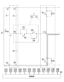
- FIG. 3 is an explanatory diagram of the discharge path and the charge path when the switching circuit 10 is in the first switching state in the multilevel inverter 100 of the first embodiment.
- the capacitor C17 is charged by the capacitor C27 if the first condition is satisfied.
- the voltages across the capacitor C17 are Vo1, Vo2, Vd1, VR1, and Vf2, respectively, the voltages across the diode D17, resistor R17, and second switching element Q2 are Vf2, the first condition is Vo2>(Vo1+Vd1+VR1+Vf2).
- the charge path Ru21 for charging the capacitor C17 by the capacitor C27 is the path of the capacitor C27-resistor R27-diode D17-resistor R17-capacitor C17-first connection point 11-second switching element Q2-capacitor C27.
- FIG. 4 is an explanatory diagram of a current path when the switching circuit 10 is in the second switching state in the multilevel inverter 100 of the first embodiment.
- the switching circuit 10 of the inverter circuit 1 When the switching circuit 10 of the inverter circuit 1 is in the second switching state and the polarity of the output current is positive, as shown in FIG. 4, the current I1 flows through the path (path indicated by the thick solid arrow) of the intermediate potential point M1 of the DC power supply unit 3-the first clamp diode D5-the second switching element Q2-the third connection point 13-the output terminal 41, and the voltage value of the output voltage to the AC load RA1 becomes 0.
- the current I1 flows through the path of the intermediate potential point M1 of the DC power supply unit 3-the first clamp diode D5 of the inverter circuit 1U-the second switching element Q2 of the switching circuit 10U-the third connection point 13-the output terminal 41.
- the switching circuit 10 of the inverter circuit 1 when the switching circuit 10 of the inverter circuit 1 is in the second switching state and the polarity of the output current is negative, as shown in FIG. 4, the current I1 flows through the path (path indicated by the thick dashed arrow) of the output terminal 41-the third connection point 13-the third switching element Q3-the second connection point 12-the second clamp diode D6, and the voltage value of the output voltage to the AC load RA1 becomes 0.
- the switching circuits 10U, 10V, and 10W are in the second switching state, the second switching state, and the first switching state, respectively, in the inverter circuit 1U, the current I1 flows through the path (path indicated by the thick dashed arrow) of the output terminal 41-the third connection point 13-the third switching element Q3-the second connection point 12-the second clamp diode D6, and the voltage value of the output voltage to the AC load RA1 becomes 0.
- FIG. 5 is an explanatory diagram of the discharge path and the charge path when the switching circuit 10 is in the second switching state in the multilevel inverter 100 of the first embodiment.
- the switching circuit 10 of the inverter circuit 1 When the switching circuit 10 of the inverter circuit 1 is in the second switching state, the voltage required to turn on the second switching element Q2 is supplied from the capacitor C27 of the second bootstrap circuit 72 to the second gate driver 62 by the second gate driver 62. Therefore, the charge of the capacitor C27 of the second bootstrap circuit 72 is discharged through the discharge path Ru2 of the capacitor C27-the high potential side power supply terminal 62H of the second gate driver 62-the low potential side power supply terminal 62L of the second gate driver 62-the capacitor C27, as shown in FIG. 5.
- the switching circuit 10 of the inverter circuit 1 when the switching circuit 10 of the inverter circuit 1 is in the second switching state, the voltage required to turn on the third switching element Q3 is supplied from the capacitor C37 of the third bootstrap circuit 73 to the third gate driver 63 by the third gate driver 63. Therefore, the charge in the capacitor C37 of the third bootstrap circuit 73 is discharged through the discharge path Ru3 from the capacitor C37 to the high potential side power supply terminal 63H of the third gate driver 63 to the low potential side power supply terminal 63L of the third gate driver 63 to the capacitor C37.
- the capacitor C27 is charged by the capacitor C37 if the second condition is met, and the capacitor C17 is charged by the capacitor C27 if the third condition is met.
- the voltages across the capacitors C17, C27, and C37 are Vo1, Vo2, and Vo3, respectively, the voltages across the diodes D17 and D27 are Vd1 and Vd2, respectively, the voltages across the resistors R17 and R27 are VR1 and VR2, respectively, and the voltages across the second switching element Q2 and the third switching element Q3 are Vf2 and Vf3, respectively, the second condition is Vo3>(Vo2+Vd2+VR2+Vf3).
- the third condition is Vo2>(Vo1+Vd1+VR1+Vf2).
- the charging path Ru32 that charges the capacitor C27 with the capacitor C37 is the path of the capacitor C37-resistor R37-diode D27-resistor R27-capacitor C27-third connection point 13-third switching element Q3-capacitor C37.
- the charging path Ru21 that charges the capacitor C17 with the capacitor C27 is the path of the capacitor C27-resistor R27-diode D17-resistor R17-capacitor C17-first connection point 11-second switching element Q2-capacitor C27.
- FIG. 6 is an explanatory diagram of a current path when the switching circuit 10 is in the third switching state in the multilevel inverter 100 of embodiment 1.
- a current I1 flows through a path from the output terminal 41-the third connection point 13-the third switching element Q3-the fourth switching element Q4-the negative pole N1 of the DC power supply unit 3, and the voltage value of the output voltage to the AC load RA1 becomes -Vdc/2.
- the capacitor C27 of the second bootstrap circuit 72 see FIG.
- the capacitor C37 of the third bootstrap circuit 73 supplies the third gate driver 63 with a voltage required to turn on the third switching element Q3 by the third gate driver 63. Therefore, the charge of the capacitor C37 of the third bootstrap circuit 73 is discharged through a discharge path Ru3 that is capacitor C37-high potential side power supply terminal 63H of the third gate driver 63-low potential side power supply terminal 63L of the third gate driver 63-capacitor C37. Also, when the switching circuit 10 of the inverter circuit 1 is in the third switching state, the capacitor C37 is charged by the power supply unit 9 when the fourth condition is met, and the capacitor C27 is charged by the capacitor C37 when the fifth condition is met.
- the fourth condition is Voo>(Vo3+Vd3+VR3+Vf4).
- the fifth condition is Vo3>(Vo2+Vd2+VR2+Vf3).
- the charging path Ru93 which charges the capacitor C37 from the power supply unit 9, is a path from the positive terminal of the power supply unit 9 to the diode D37 to the resistor R37 to the capacitor C37 to the second connection point 12 to the fourth switching element Q4 to the negative terminal of the power supply unit 9.
- the charging path Ru32 which charges the capacitor C27 from the capacitor C37, is a path from the capacitor C37 to the resistor R37 to the diode D27 to the resistor R27 to the capacitor C27 to the third connection point 13 to the third switching element Q3 to the capacitor C37.
- the control unit 60 generates first to fourth control signals S1 to S4 (S1U to S4U) for the first to fourth switching elements Q1 to Q4 of the inverter circuit 1U, first to fourth control signals S1 to S4 (S1V to S4V) for the first to fourth switching elements Q1 to Q4 of the inverter circuit 1V, and first to fourth control signals S1 to S4 (S1W to S4W) for the first to fourth switching elements Q1 to Q4 of the inverter circuit 1W, based on the voltage commands Vu, Vv, and Vw (see FIG. 8) related to the output voltages of the inverter circuits 1U, 1V, and 1W, respectively.
- the control unit 60 may perform PI (Proportional Integral) control of the voltage commands Vu, Vv, and Vw based on information output from the detection unit 8 that detects the state of the AC load RA1.
- PI Proportional Integral
- the information output from the detection unit 8 includes, for example, at least one of the following: information on the detection results of a plurality of current sensors that detect the output currents flowing through the U-phase, V-phase, and W-phase of the AC load RA1; and information on the detection results of an encoder that detects the rotation speed, rotation angle, etc. of the three-phase motor.
- one of the three inverter circuits 1 (for example, the U-phase inverter circuit 1U) will be described.
- the operation of the V-phase inverter circuit 1V and the W-phase inverter circuit 1W is similar to that of the U-phase inverter circuit 1U.
- the output voltages of the U-phase inverter circuit 1U, the V-phase inverter circuit 1V, and the W-phase inverter circuit 1W are out of phase with each other.
- the control unit 60 controls a plurality of first gate drivers 61, a plurality of second gate drivers 62, a plurality of third gate drivers 63, and a plurality of fourth gate drivers 64 by performing voltage vector control.
- the voltage vector control by the control unit 60 is explained in more detail below.
- the control unit 60 stores a group of voltage vectors in advance.
- Each of the group of voltage vectors is determined by a combination of the potential levels of the connection point (third connection point 13) between the second switching element Q2 and the third switching element Q3 of the multiple inverter circuits 1.
- the group of voltage vectors is determined by the switching state of the switching circuit 10U corresponding to the U phase, the switching state of the switching circuit 10V corresponding to the V phase, and the switching state of the switching circuit 10W corresponding to the W phase.
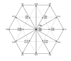
- the group of voltage vectors includes three zero vectors V0p, V0n, and V0o, each of which has a magnitude of zero.
- the group of voltage vectors also includes six voltage vectors V1, V2, V3, V4, V5, and V6, each of which has a magnitude of (2/3)1/2 ⁇ 2 Vdc and has different directions.
- the group of voltage vectors also includes 12 voltage vectors V7p, V7n, V8p, V8n, V9p, V9n, V10p, V10n, V11p, V11n, V12p, and V12n, each of which has a magnitude of (2/3)1/2 ⁇ Vdc.
- the group of voltage vectors includes six voltage vectors V13, V14, V15, V16, V17, and V18, each of which has a magnitude of (2/3)1/2 ⁇ 31/2 ⁇ Vdc and a different direction.
- the angle between two adjacent voltage vectors among the six voltage vectors V1, V2, V3, V4, V5, and V6 is 60 degrees.
- the angle between two adjacent voltage vectors among the six voltage vectors V13, V14, V15, V16, V17, and V18 is also 60 degrees.
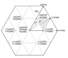
- FIG. 9 is a vector diagram illustrating the group of voltage vectors on an orthogonal d-q coordinate system.
- the group of voltage vectors can be expressed as shown in Figure 10 by expressing the first switching state, the second switching state, and the third switching state with the symbols "P", “0", and “N”, respectively, and listing the U phase, V phase, and W phase in that order.
- V0p[PPP] expresses that, with respect to the zero vector V0p, the switching state of the U-phase switching circuit 10U is "P", the switching state of the V-phase switching circuit 10V is "P”, and the switching state of the W-phase switching circuit 10W is "P".
- a voltage vector with "p" attached, such as V10p includes "P” and does not include "N”.
- a voltage vector with "n” attached, such as V10n includes “N” and does not include “P”.
- voltage vectors with “o” attached, such as V10o include “0” and do not include “P” or “N”.
- V1, V2, V3, V4, V5, and V6 can be expressed as V1[PNN], V2[PPN], V3[NPN], V4[NPP], V5[NNP], and V6[PNP], respectively.
- Voltage vectors that do not have "p,” "n,” or "o” added after the number added to "V,” such as V1[PNN], V2[PPN], V3[NPN], V4[NPP], V5[NNP], and V6[PNP] include "P" and "N” as the switching states of the three phases.
- the 12 voltage vectors V7p, V7n, V8p, V8n, V9p, V9n, V10p, V10n, V11p, V11n, V12p, and V12n can be expressed as V7p[P00], V7n[0NN], V8p[PP0], V8n[00N], V9p[0P0], V9n[N0N], V10p[0PP], V10n[N00], V11p[00P], V11n[NN0], V12p[P0P], and V12n[0N0], respectively.
- V13, V14, V15, V16, V17, and V18 can be expressed as V13[P0N], V14[0PN], V15[NP0], V16[N0P], V17[0NP], and V18[PN0], respectively.
- the control unit 60 converts the instantaneous value of the command voltage for the output voltage of each of the multiple inverter circuits 1 into a command voltage vector V* (see FIG. 11). If the d-axis component of the command voltage vector V* on the orthogonal d-q coordinate system is Vd and the q-axis component of the command voltage vector V* on the orthogonal d-q coordinate system is Vq, the command voltage vector V* can be calculated using equation (1).
- the control unit 60 selects a plurality of (e.g., five) voltage vectors adjacent to the command voltage vector V* from the group of voltage vectors.
- FIG. 11 is a vector diagram for explaining the operation of the control unit 60 in the multilevel inverter 100 of the first embodiment.
- the plurality of voltage vectors are V8p[PP0], V8n[00N], V13[P0N], V7p[P00], and V7n[0NN].
- the angle between the voltage vector closest to the command voltage vector V* (hereinafter also referred to as voltage vector VV1) and the command voltage vector V* is less than 30 degrees.
- the control unit 60 within a given control period Ts, matches the resultant vector of the vectors of the vertices of an equilateral triangle surrounding the command voltage vector V* with the command voltage vector V*. That is, the control unit 60 matches the resultant vector of the voltage vector VV1 (V8p[PP0] and V8n[00N] in the example of FIG. 11), the voltage vector V13[P0N], and the voltage vectors V7p[P00] and V7n[0NN] with the command voltage vector V*.
- the control period Ts is one period of the carrier signal.
- the switching state of only one of the U, V, and W phases in two voltage vectors arranged in time series changes between "P" and "0” or between "0” and “N", and the same voltage vector is output twice.
- the voltage vector V8n[00N] ⁇ voltage vector V13[P0N] ⁇ voltage vector V7p[P00] ⁇ voltage vector V8p[PP0] ⁇ voltage vector V8p[PP0] ⁇ voltage vector V7p[P00] ⁇ voltage vector V13[P0N] ⁇ voltage vector V8n[00N] are output in this order.
- the voltage vector Va is the voltage vector V8p[PP0] and V8n[00N]
- the voltage vector Vb is the voltage vector V13[P0N]
- the voltage vector Vc is the voltage vector V7p[P00] and V7n[0NN].
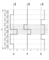
- FIG. 12 is a diagram showing a time chart of the switching state of each phase of the multilevel inverter 100 of embodiment 1.
- the on/off states of the first switching element Q1, the second switching element Q2, the third switching element Q3, and the fourth switching element Q4 are as shown in FIG. 13 within the control period Ts.
- FIG. 13 is a diagram showing a time chart of the on/off states of the first to fourth switching elements (Q1 to Q4) of the multilevel inverter 100 of embodiment 1.
- the second switching element Q2 is in the on state for the entire period within the control period Ts, and the voltage drop width of the second bootstrap circuit 72 becomes large.
- the order of the voltage vectors within the control period Ts may differ depending on the initial value of the carrier signal at the start of the control period Ts.
- FIG. 14A is a timing chart showing the relationship between the control signal to the switching elements (Q1 to Q4) when the switching elements (Q1 to Q4) are turned on and the current flowing through the control terminal of the switching elements (Q1 to Q4).
- the multilevel inverter 100 when the potential level of the control signal S1 to each of the multiple first switching elements Q1 changes from a low level ("L" in FIG. 14A) to a high level ("H" in FIG. 14A), a pulsed current (see FIG. 14A) flows through the control terminal of the first switching element Q1 that is turned on. This consumes the charge of the capacitor C17 of the bootstrap circuit 71 that corresponds to the first switching element Q1 that is turned on among the multiple bootstrap circuits 71.
- FIG. 14B is a timing chart showing the relationship between the control signal to the switching elements (Q1 to Q4) and the current flowing through the control terminal of the switching elements (Q1 to Q4) when the switching elements (Q1 to Q4) are turned off.
- a pulsed current flows through the control terminal of the first switching element Q1 that is turned off. This consumes the charge of the capacitor C17 of the bootstrap circuit 71 that corresponds to the first switching element Q1 that is turned on among the multiple bootstrap circuits 71.
- the carrier frequency is the frequency of the carrier signal that is determined by the period of the carrier signal.
- FIG. 15A is a diagram showing the carrier frequency dependence of the voltage change of capacitor C17 in the multilevel inverter 100 of embodiment 1.
- FIG. 15A shows the time change of the voltage of capacitor C17 (the voltage Vo1 across both ends described above) when the carrier frequency is changed with the capacitance of capacitor C17 set to 0.2 ⁇ F.
- “A1” shows the time change of the voltage of capacitor C17 when the carrier frequency is set to 6 kHz
- “A2” shows the time change of the voltage of capacitor C17 when the carrier frequency is set to 12 kHz
- “A3” shows the time change of the voltage of capacitor C17 when the carrier frequency is set to 20 kHz.
- FIG. 15B is a diagram showing the capacitance dependency of the voltage change of capacitor C17 in the multilevel inverter 100 of embodiment 1. It shows the time change of the voltage of capacitor C17 when the carrier frequency is set to 20 kHz and the capacitance of capacitor C17 is changed.
- "A4" shows the time change of the voltage of capacitor C17 when the capacitance of capacitor C17 is set to 0.2 ⁇ F
- "A5" shows the time change of the voltage of capacitor C17 when the capacitance of capacitor C17 is set to 1 ⁇ F
- “A6” shows the time change of the voltage of capacitor C17 when the capacitance of capacitor C17 is set to 10 ⁇ F.
- the capacitance of each of the capacitors C17 in the multiple first bootstrap circuits 71 is set to a value of 10 ⁇ F or more and 50 ⁇ F or less.
- the capacitance of each of the capacitors C27 in the multiple second bootstrap circuits 72 is set to a value of 10 ⁇ F or more and 50 ⁇ F or less.
- the capacitance of each of the capacitors C37 in the multiple third bootstrap circuits 73 is set to a value of 10 ⁇ F or more and 50 ⁇ F or less.
- the capacitance of each of the capacitors C17, C27, and C37 is set, for example, according to the value of the carrier frequency. How to determine the capacitance of each of the capacitors C17, C27, and C37 will be explained with reference to Figures 16 to 18 after explaining the operation of the control unit of the multilevel inverter according to the comparative example with reference to Figures 19A, 19B, 20, and 21.
- a control unit performs control to replace some voltage vectors with other voltage vectors in voltage vector control.
- the control unit selects multiple (e.g., five) voltage vectors that are adjacent to the command voltage vector V* (see FIG. 19A) from the group of voltage vectors.
- FIG. 19A is an explanatory diagram of the command voltage vector and the first voltage vector for a multilevel inverter according to a comparative example.
- the multiple voltage vectors are V8p[PP0], V8n[00N], V13[P0N], V7p[P00], and V7n[0NN].
- the control unit replaces one of the two first voltage vectors VV1 (V8p[PP0] and V8n[00N] in the example of FIG. 19A), which are the two voltage vectors VV1 whose magnitude is a reference magnitude and closest to the command voltage vector V*, with a zero vector V0n[NNN] in which the potential level of the third connection point 13 of the multiple inverter circuits 1 is a negative potential, and at least one second voltage vector VV2 (V2[PPN] in the example of FIG. 19A) that has the same direction as the first voltage vector VV1 but a different magnitude from the first voltage vector VV1.
- the reference magnitude is, for example, (2/3)1/2 ⁇ Vdc.
- the multiple voltage vectors include 12 voltage vectors V7p[P00], V7n[0NN], V8p[PP0], V8n[00N], V9p[0P0], V9n[N0N], V10p[0PP], V10n[N00], V11p[00P], V11n[NN0], V12p[P0P], and V12n[0N0] as voltage vectors whose magnitude is a reference magnitude (reference vectors).
- the angle between the command voltage vector V* and the two first voltage vectors VV1 closest to the command voltage vector V* is less than 30 degrees.
- FIG. 19B is an explanatory diagram of a command voltage vector, a zero vector, and a second voltage vector for a multilevel inverter of a comparative example.
- the control unit controls the first gate drivers, the second gate drivers, the third gate drivers, and the fourth gate drivers within a predetermined control period Ts (see FIG. 20) so that the composite vector of three voltage vectors (V13[P0N], V7p[P00], and V7n[0NN] in the example of FIG. 19B) other than the first voltage vector VV1 (V8p[PP0] and V8n[00N] in the example of FIG. 19A), the zero vector V0n[NNN], and at least one second voltage vector VV2 coincides with the command voltage vector V*.
- the predetermined control period Ts is, for example, two periods of the carrier signal.
- FIG. 20 is a diagram showing a time chart of the switching state of each phase when the inverter circuit of each phase is controlled by replacing the first voltage vector with a zero vector and a second voltage vector in a multilevel inverter of a comparative example.
- the on/off of the first switching element Q1, the second switching element Q2, the third switching element Q3, and the fourth switching element Q4 is as shown in FIG. 21 within a control period Ts.
- FIG. 21 is a diagram showing a time chart of the on/off state of the first to fourth switching elements when the inverter circuit is controlled by replacing the first voltage vector with a zero vector and a second voltage vector in a multilevel inverter of a comparative example.
- control unit may replace the first voltage vector VV1 with the zero vector V0n [NNN] and the second voltage vector VV2 only when the polarity of the command voltage corresponding to the command voltage vector V* is positive, and may also replace the first voltage vector VV1 with the zero vector V0n [NNN] and the second voltage vector VV2 when the polarity of the command voltage is negative.
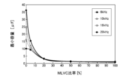
- FIG. 16 is a graph showing the results of a simulation of the relationship between the minimum capacitance of the capacitor C17 included in the first bootstrap circuit 71, the carrier frequency, and the multilevel vector control (MLVC) ratio.
- the "minimum capacitance” means the lower limit of the capacitance of the capacitor C17 required to maintain the voltage value of the gate voltage required to turn on and off the first switching element Q1 in the capacitor C17.
- the "MLVC ratio" indicates the ratio at which the voltage vector control of the comparative example is performed relative to the voltage vector control of the first embodiment, and when the value of the MLVC ratio is 0, it means that only the voltage vector control of the first embodiment is performed, and the voltage vector control of the comparative example is not performed. In addition, the greater the value of the MLVC ratio is than 0, the higher the frequency of replacing the voltage vector in the voltage vector control of the comparative example.
- the defined plane PL1 surrounded by a thick line is a plane that defines the minimum capacitance of capacitor C17 required to maintain the gate voltage value (e.g., 11 V) required to turn the first switching element Q1 on and off in capacitor C17. Therefore, if the capacitance of capacitor C17 is greater than the minimum capacitance of any point of the combination of carrier frequency and MLVC ratio in FIG. 16 projected vertically onto defined plane PL1, it becomes possible to maintain the gate voltage value required to turn the first switching element Q1 on and off in capacitor C17.
- the gate voltage value e.g. 11 V
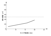
- FIG. 17 is a graph showing the results of a simulation of the relationship between the minimum capacitance of capacitor C17 included in the first bootstrap circuit 71 and the carrier frequency. It can be seen from FIG. 17 that the minimum capacitance of capacitor C17 increases as the carrier frequency increases. Note that FIG. 17 is a graph for the case in FIG. 16 where the HLVC ratio is 0%.
- Figure 18 is a graph showing the relationship between the minimum capacitance of capacitor C17 included in the first bootstrap circuit 71 and the MLVC ratio.
- Figure 18 shows the relationship between the minimum capacitance of capacitor C17 and the MLVC ratio when the carrier frequency in Figure 16 is 6 kHz, 10 kHz, 16 kHz, and 20 kHz. It can be seen from Figure 18 that the minimum capacitance of capacitor C17 increases as the carrier frequency increases. It can also be seen from Figure 18 that the minimum capacitance of capacitor C17 can be reduced by increasing the MLVC ratio.
- the upper limit of the minimum capacitance of each of the capacitors C17 in the first bootstrap circuits 71 is preferably 50 ⁇ F, from the viewpoint of using a capacitor smaller than an aluminum electrolytic capacitor as the capacitor C17. Therefore, it is preferable that the capacitance of each of the capacitors C17 in the first bootstrap circuits 71 is 10 ⁇ F or more and 50 ⁇ F or less.
- the capacitor C17 of each of the multiple first bootstrap circuits 71 is, for example, a multilayer ceramic capacitor, a film capacitor, or a tantalum electrolytic capacitor.
- the minimum capacitance of each of the capacitors C17 in the multiple first bootstrap circuits 71 has been described above, but the same applies to the minimum capacitance of each of the capacitors C27 in the multiple second bootstrap circuits 72 and the minimum capacitance of each of the capacitors C37 in the multiple third bootstrap circuits 73.
- the capacitance of the capacitor C17 included in each of the first bootstrap circuits 71 is not less than 10 ⁇ F and not more than 50 ⁇ F.
- the control unit 60 can maintain the voltage of the capacitor C17 of the multiple first bootstrap circuits 71 at or above the voltage required to turn the first switching element Q1 on and off without performing special voltage vector control to replace the voltage vector.
- the capacitance of the capacitor C27 included in each of the second bootstrap circuits 72 is 10 ⁇ F or more and 50 ⁇ F or less.
- the above configuration makes it possible to suppress the voltage drop of the capacitor C27 of the second bootstrap circuit 72.
- the capacitance of the capacitor C37 included in each of the third bootstrap circuits 73 is 10 ⁇ F or more and 50 ⁇ F or less.
- the above configuration makes it possible to suppress the voltage drop of the capacitor C37 of the third bootstrap circuit 73.
- the DC-DC converter 91 included in the power supply unit 9 supplies voltage to the multiple fourth gate drivers 64 and the multiple third bootstrap circuits 73. This makes it possible for the multilevel inverter 100 according to the first embodiment to suppress voltage drops in each of the multiple third bootstrap circuits 73 while achieving miniaturization.
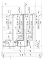
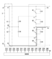
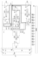
- the multilevel inverter 100A includes, for example, a DC power supply unit 3, a plurality of (three in the example of Fig. 22) inverter circuits 1, and a control device 6, as shown in Fig. 22.
- the DC power supply unit 3 has a positive electrode P1, a negative electrode N1, and an intermediate potential point M1.
- the plurality of inverter circuits 1 are connected between the positive electrode P1 and the negative electrode N1 of the DC power supply unit 3.
- the control device 6 controls the plurality of inverter circuits 1.
- the multilevel inverter 100A is a T-type three-level three-phase inverter.
- each of the multiple inverter circuits 1 has an output terminal 41.
- an AC load RA1 is connected to multiple (three in the example of FIG. 22) output terminals (AC terminals) 41.
- the AC load RA1 is, for example, a three-phase servo motor.
- one of the multiple inverter circuits 1 is an inverter circuit 1U that outputs a U-phase voltage
- another is an inverter circuit 1V that outputs a V-phase voltage
- the remaining one is an inverter circuit 1W that outputs a W-phase voltage.
- Each of the multiple inverter circuits 1 has a first switching element Q1, a second switching element Q2, a third switching element Q3, and a fourth switching element Q4, and a first diode D1, a second diode D2, a third diode D3, and a fourth diode D4.
- the first diode D1, the second diode D2, the third diode D3, and the fourth diode D4 are connected in anti-parallel to the first switching element Q1, the second switching element Q2, the third switching element Q3, and the fourth switching element Q4, respectively.
- the first switching element Q1 and the second switching element Q2 are connected in series from the positive pole P1 side to the negative pole N1 side in the order of the first switching element Q1 and the second switching element Q2.
- a series circuit (first circuit 111) of the first switching element Q1 and the second switching element Q2 is connected between the positive pole P1 and the negative pole N1.
- a series circuit (second circuit 112) of a third switching element Q3 and a fourth switching element Q4 is connected between an intermediate potential point M1 and an output point.
- the output point is a connection point 113 between the first switching element Q1 and the second switching element Q2.
- the second circuit 112 has a bidirectional switch including the third switching element Q3, the fourth switching element Q4, the third diode D3, and the fourth diode D4.
- the control device 6 has a plurality of first gate drivers 61 (three in the example of FIG. 22), a plurality of second gate drivers 62 (three in the example of FIG. 22), a plurality of third gate drivers 63 (three in the example of FIG. 22), and a plurality of fourth gate drivers 64 (three in the example of FIG. 22).
- the control device 6 also has a plurality of bootstrap circuits 71 (hereinafter also referred to as first bootstrap circuits 71) (three in the example of FIG. 22), a plurality of second bootstrap circuits 72 (three in the example of FIG. 22), a power supply unit 9, and a control unit 60.
- the multiple first gate drivers 61 drive the first switching elements Q1 of the multiple inverter circuits 1.
- the multiple second gate drivers 62 drive the second switching elements Q2 of the multiple inverter circuits 1.
- the multiple third gate drivers 63 drive the third switching elements Q3 of the multiple inverter circuits 1.
- the multiple fourth gate drivers 64 drive the fourth switching elements Q4 of the multiple inverter circuits 1.
- the multiple first bootstrap circuits 71 correspond one-to-one to the multiple first gate drivers 61. Each of the multiple first bootstrap circuits 71 supplies a voltage to a corresponding first gate driver 61 among the multiple first gate drivers 61.
- the multiple second bootstrap circuits 72 correspond to the multiple third gate drivers 63 and the multiple fourth gate drivers 64. Each of the multiple second bootstrap circuits 72 supplies a voltage to a corresponding third gate driver 63 and a corresponding fourth gate driver 64 among the multiple third gate drivers 63.
- the power supply unit 9 supplies a voltage to the multiple second gate drivers 62.
- the control unit 60 controls a plurality of first gate drivers 61, a plurality of second gate drivers 62, a plurality of third gate drivers 63, and a plurality of fourth gate drivers 64.
- the DC power supply unit 3 has a first capacitor C1 and a second capacitor C2.
- the first capacitor C1 and the second capacitor C2 are connected in series.
- a first end of the first capacitor C1 is connected to a first DC terminal 31
- a second end of the first capacitor C1 is connected to a first end of the second capacitor C2
- a second end of the second capacitor C2 is connected to a second DC terminal 32.
- a connection point between the first capacitor C1 and the second capacitor C2 is an intermediate potential point M1.
- the DC power supply unit 3 further has a first DC terminal 31 connected to a positive pole P1 and a second DC terminal 32 connected to a negative pole N1.
- a DC voltage source E1 is connected between the first DC terminal 31 and the second DC terminal 32.
- the output voltage Vdc of the DC voltage source E1 is applied between the positive electrode P1 and the negative electrode N1 of the DC power supply unit 3.
- the capacitance of the second capacitor C2 is the same as the capacitance of the first capacitor C1.
- the capacitance of the second capacitor C2 is the same as the capacitance of the first capacitor C1
- the output terminal 41 included in the inverter circuit 1U among the multiple output terminals 41 may be referred to as the output terminal 41U
- the output terminal 41 included in the inverter circuit 1V may be referred to as the output terminal 41V
- the output terminal included in the inverter circuit 1W may be referred to as the output terminal 41W.
- the first switching element Q1, the second switching element Q2, the third switching element Q3, and the fourth switching element Q4 of each inverter circuit 1 have a control terminal, a first main terminal, and a second main terminal.
- the first switching element Q1, the second switching element Q2, the third switching element Q3, and the fourth switching element Q4 of each inverter circuit 1 are, for example, IGBTs. Therefore, the control terminal, the first main terminal, and the second main terminal of each of the first switching element Q1, the second switching element Q2, the third switching element Q3, and the fourth switching element Q4 of each inverter circuit 1 are the gate terminal, the collector terminal, and the emitter terminal, respectively.
- the control terminal of the first switching element Q1 of each inverter circuit 1 is connected to a corresponding first gate driver 61 of the multiple first gate drivers 61. Also, the control terminal of the second switching element Q2 of each inverter circuit 1 is connected to a corresponding second gate driver 62 of the multiple second gate drivers 62. Also, the control terminal of the third switching element Q3 of each inverter circuit 1 is connected to a corresponding third gate driver 63 of the multiple third gate drivers 63. Also, the control terminal of the fourth switching element Q4 of each inverter circuit 1 is connected to a corresponding fourth gate driver 64 of the multiple fourth gate drivers 64.
- the first main terminal of the first switching element Q1 is connected to the positive pole P1 of the DC power supply unit 3
- the second main terminal of the first switching element Q1 is connected to the first main terminal of the second switching element Q2
- the second main terminal of the second switching element Q2 is connected to the negative pole N1 of the DC power supply unit 3.
- the bidirectional switch of the second circuit 112 is a common emitter bidirectional switch in which the second main terminals (emitter terminals) of the third switching element Q3 and the fourth switching element Q4 are connected to each other.
- the "intermediate potential point M1" is a point that is an intermediate potential between the potential of the positive electrode P1 and the potential of the negative electrode N1 of the DC power supply unit 3.
- the potential of the intermediate potential point M1 is 0V.
- the potential of the positive electrode P1 is Vdc/2
- the potential of the negative electrode N1 is -Vdc/2.
- connection point 113 between the first switching element Q1 and the second switching element Q2 is connected to the output terminal 41U.
- the connection point 113 between the first switching element Q1 and the second switching element Q2 is connected to the output terminal 41V.
- connection point 113 between the first switching element Q1 and the second switching element Q2 is connected to the output terminal 41W.
- the connection point 113 of the inverter circuit 1U is connected to, for example, the U phase of the AC load RA1 via the output terminal 41U.
- the connection point 113 of the inverter circuit 1V is connected to, for example, the V phase of the AC load RA1 via the output terminal 41V.
- the connection point 113 of the inverter circuit 1W is connected to, for example, the W phase of the AC load RA1 via the output terminal 41W.
- the anode of the first diode D1 is connected to the second main terminal (emitter terminal) of the first switching element Q1, and the cathode of the first diode D1 is connected to the first main terminal (collector terminal) of the first switching element Q1.
- the anode of the second diode D2 is connected to the second main terminal (emitter terminal) of the second switching element Q2, and the cathode of the second diode D2 is connected to the first main terminal (collector terminal) of the second switching element Q2.
- the anode of the third diode D3 is connected to the second main terminal (emitter terminal) of the third switching element Q3, and the cathode of the third diode D3 is connected to the first main terminal (collector terminal) of the third switching element Q3.
- the anode of the fourth diode D4 is connected to the second main terminal (emitter terminal) of the fourth switching element Q4, and the cathode of the fourth diode D4 is connected to the first main terminal (collector terminal) of the fourth switching element Q4.
- the first diode D1 may be replaced by a parasitic diode of the IGBT that constitutes the first switching element Q1.
- the second diode D2 may be replaced by a parasitic diode of the IGBT that constitutes the second switching element Q2.
- the third diode D3 may be replaced by a parasitic diode of the IGBT that constitutes the third switching element Q3.
- the fourth diode D4 may be replaced by a parasitic diode of the IGBT that constitutes the fourth switching element Q4.
- the multiple first gate drivers 61 correspond one-to-one to the multiple first switching elements Q1. Each of the multiple first gate drivers 61 is connected to a control terminal of a corresponding first switching element Q1 among the multiple first switching elements Q1. The multiple first gate drivers 61 drive the corresponding first switching element Q1. The multiple first gate drivers 61 are connected to a control unit 60. The control unit 60 outputs multiple first control signals S1 (see FIG. 23) that correspond one-to-one to the multiple first gate drivers 61. Each of the multiple first gate drivers 61 controls the on/off of the first switching element Q1 based on the given first control signal S1.
- the second gate drivers 62 correspond one-to-one to the second switching elements Q2. Each of the second gate drivers 62 is connected to a control terminal of a corresponding one of the second switching elements Q2. The second gate drivers 62 drive the corresponding second switching element Q2. The second gate drivers 62 are connected to the control unit 60.
- the control unit 60 outputs second control signals S2 (see FIG. 23) that correspond one-to-one to the second gate drivers 62.
- Each of the second gate drivers 62 controls the on/off of the second switching element Q2 based on the second control signal S2 provided.
- the multiple third gate drivers 63 correspond one-to-one to the multiple third switching elements Q3.
- Each of the multiple third gate drivers 63 is connected to a control terminal of a corresponding one of the multiple third switching elements Q3.
- the multiple third gate drivers 63 drive the corresponding third switching element Q3.
- the multiple third gate drivers 63 are connected to the control unit 60.
- the control unit 60 outputs multiple third control signals S3 (see FIG. 2) that correspond one-to-one to the multiple third gate drivers 63.
- Each of the multiple third gate drivers 63 controls the on/off of the third switching element Q3 based on the provided third control signal S3.
- the multiple fourth gate drivers 64 correspond one-to-one to the multiple fourth switching elements Q4. Each of the multiple fourth gate drivers 64 is connected to a control terminal of a corresponding one of the multiple fourth switching elements Q4. The multiple fourth gate drivers 64 drive the corresponding fourth switching element Q4. The multiple fourth gate drivers 64 are connected to the control unit 60.
- the control unit 60 outputs multiple fourth control signals S4 (see FIG. 23) that correspond one-to-one to the multiple fourth gate drivers 64.
- Each of the multiple fourth gate drivers 64 controls the on/off of the fourth switching element Q4 based on the provided fourth control signal S4.
- the first bootstrap circuits 71 correspond one-to-one to the first gate drivers 61.
- the first bootstrap circuits 71 supply voltages to the corresponding first gate drivers 61.
- each of the first bootstrap circuits 71 has a diode D17, a resistor R17, and a capacitor C17 (also called a boost capacitor C17).
- the anode of the diode D17 is connected to the positive terminal of the power supply unit 9, and the cathode of the diode D17 is connected to a first end of the capacitor C17 via the resistor R17.
- the first end of the capacitor C17 is connected to the high-potential power supply terminal 61H (see FIG.
- the first bootstrap circuit 71 supplies the first gate driver 61 with a voltage required to turn on the first switching element Q1 in the first gate driver 61.
- Each of the first bootstrap circuits 71 further includes a Zener diode Z17 connected in parallel to the capacitor C17.
- the multiple second bootstrap circuits 72 correspond to the multiple third gate drivers 63 and the multiple fourth gate drivers 64.
- the multiple second bootstrap circuits 72 supply voltages to the corresponding third gate drivers 63 and the corresponding fourth gate drivers 64.
- Each of the multiple second bootstrap circuits 72 has a diode D27, a resistor R27, and a capacitor C27 (also referred to as a boost capacitor C27).
- the anode of the diode D27 is connected to the positive terminal of the power supply unit 9, and the cathode of the diode D27 is connected to a first end of the capacitor C27 via the resistor R27.
- the first end of the capacitor C27 is connected to the high potential side power supply terminal 63H (see FIG.
- the second bootstrap circuit 72 supplies the third gate driver 63 with a voltage required to turn on the third switching element Q3 in the third gate driver 63, and supplies the fourth gate driver 64 with a voltage required to turn on the fourth switching element Q4 in the fourth gate driver 64.
- Each of the second bootstrap circuits 72 further includes a Zener diode Z27 connected in parallel to the capacitor C27.
- the power supply unit 9 supplies voltage to a plurality of (three in the example of FIG. 22) first bootstrap circuits 71, a plurality of (three in the example of FIG. 22) second bootstrap circuits 72, and a plurality of (three in the example of FIG. 22) second gate drivers 62.
- the power supply unit 9 is, for example, a DC power supply including an isolated DC-DC converter 91.
- the positive terminal of the power supply unit 9 is connected to the high potential power supply terminal 62H (see FIG. 24) of each of the second gate drivers 62, and the negative terminal of the power supply unit 9 is connected to the low potential power supply terminal 62L (see FIG. 24) of each of the second gate drivers 62.
- the control unit 60 controls a plurality of first gate drivers 61, a plurality of second gate drivers 62, a plurality of third gate drivers 63, and a plurality of fourth gate drivers 64.
- the control unit 60 controls a plurality of first switching elements Q1, a plurality of second switching elements Q2, a plurality of third switching elements Q3, and a plurality of fourth switching elements Q4.
- the execution subject of the control unit 60 includes a computer system.
- the computer system has one or more computers.
- the computer system is mainly composed of a processor and a memory as hardware.
- the processor executes a program recorded in the memory of the computer system, thereby realizing the function of the control unit 60 as the execution subject in this disclosure.
- the program may be pre-recorded in the memory of the computer system, or may be provided through an electric communication line, or may be recorded and provided on a non-transitory recording medium such as a memory card, an optical disk, or a hard disk drive (magnetic disk) that can be read by the computer system.
- the processor of the computer system is composed of one or more electronic circuits including a semiconductor integrated circuit (IC) or a large-scale integrated circuit (LSI).
- the multiple electronic circuits may be integrated into one chip, or may be distributed across multiple chips.
- the multiple chips may be integrated into one device, or may be distributed across multiple devices.
- the control unit 60 outputs a plurality (three) of first control signals S1 (see FIG. 23) for controlling a plurality (three) of first switching elements Q1, a plurality (three) of second control signals S2 (see FIG. 23) for controlling a plurality (three) of second switching elements Q2, a plurality (three) of third control signals S3 (see FIG. 23) for controlling a plurality (three) of third switching elements Q3, and a plurality (three) of fourth control signals S4 (see FIG. 23) for controlling a plurality (three) of fourth switching elements Q4.
- first control signals S1 see FIG. 23
- second control signals S2 for controlling a plurality (three) of second switching elements Q2
- a plurality (three) of third control signals S3 for controlling a plurality (three) of third switching elements Q3
- a plurality (three) of fourth control signals S4 for controlling a plurality (three) of fourth switching elements Q4.
- a plurality of first gate drivers 61, a plurality of second gate drivers 62, a plurality of third gate drivers 63, a plurality of fourth gate drivers 64, a plurality of first bootstrap circuits 71, a plurality of second bootstrap circuits 72, and a power supply unit 9 are omitted from illustration.
- FIG. 24 only one of the three inverter circuits 1 is shown, and the remaining two inverter circuits 1 are omitted.
- the two first gate drivers 61, the two second gate drivers 62, the two third gate drivers 63, the two fourth gate drivers 64, the two first bootstrap circuits 71, and the two second bootstrap circuits 72 are omitted.
- the three first control signals S1 include a first control signal S1U that controls the first switching element Q1 of the inverter circuit 1U, a first control signal S1V that controls the first switching element Q1 of the inverter circuit 1V, and a first control signal S1W that controls the first switching element Q1 of the inverter circuit 1W.
- the three second control signals S2 include a second control signal S2U that controls the second switching element Q2 of the inverter circuit 1U, a second control signal S2V that controls the second switching element Q2 of the inverter circuit 1V, and a second control signal S2W that controls the second switching element Q2 of the inverter circuit 1W.
- the three third control signals S3 include a third control signal S3U that controls the third switching element Q3 of the inverter circuit 1U, a third control signal S3V that controls the third switching element Q3 of the inverter circuit 1V, and a third control signal S3W that controls the third switching element Q3 of the inverter circuit 1W.
- the three fourth control signals S4 include a fourth control signal S4U that controls the fourth switching element Q4 of the inverter circuit 1U, a fourth control signal S4V that controls the fourth switching element Q4 of the inverter circuit 1V, and a fourth control signal S4W that controls the fourth switching element Q4 of the inverter circuit 1W.
- Each of the multiple first control signals S1, multiple second control signals S2, multiple third control signals S3, and multiple fourth control signals S4 is, for example, a signal whose potential level changes between a first potential level (hereinafter also referred to as a low level) and a second potential level (hereinafter also referred to as a high level) that is higher than the first potential level.
- the first potential level is, for example, 0V
- the second potential level is a potential level higher than the gate threshold voltage of the IGBT.
- the first potential level is a potential level for turning off the switching element corresponding to that control signal
- the second potential level is a potential level for turning on the switching element corresponding to that control signal
- Each of the multiple first switching elements Q1 is turned on when the corresponding first control signal S1 is at a high level, and turned off when it is at a low level.
- Each of the multiple second switching elements Q2 is turned on when the corresponding second control signal S2 is at a high level, and turned off when it is at a low level.
- Each of the multiple third switching elements Q3 is turned on when the corresponding third control signal S3 is at a high level, and turned off when it is at a low level.
- Each of the multiple fourth switching elements Q4 is turned on when the corresponding fourth control signal S4 is at a high level, and turned off when it is at a low level.
- each of the multiple inverter circuits 1 is controlled to a first switching state, a second switching state, or a third switching state. That is, in the multilevel inverter 100A, the switching state is controlled to one of the first switching state, the second switching state, and the third switching state in each of the three inverter circuits 1U, 1V, and 1W.
- the first switching state, the second switching state, and the third switching state have different combinations of on/off states of the first to fourth switching elements Q1 to Q4.
- the output voltage in the first switching state, the output voltage in the second switching state, and the output voltage in the third switching state are different from each other.
- the potential level of the output voltage changes in three levels depending on the state of the first to fourth switching elements Q1 to Q4.
- the output voltage of the U-phase inverter circuit 1U, the output voltage of the V-phase inverter circuit 1V, and the output voltage of the W-phase inverter circuit 1W are in different phases from each other.
- the first switching state is a combination in which both the first switching element Q1 and the third switching element Q3 are in the on state, and both the second switching element Q2 and the fourth switching element Q4 are in the off state.
- each of the multiple inverter circuits 1 can output an output voltage at the potential level of the positive electrode P1 of the DC power supply unit 3.
- each of the multiple inverter circuits 1 has the potential of the connection point 113 at the potential level of the positive electrode P1 of the DC power supply unit 3 (e.g., Vdc/2).
- the second switching state is a combination in which both the first switching element Q1 and the second switching element Q2 are in the off state, and both the third switching element Q3 and the fourth switching element Q4 are in the on state.
- each of the multiple inverter circuits 1 can output an output voltage at the potential level of the intermediate potential point M1 of the DC power supply unit 3.
- each of the multiple inverter circuits 1 has the potential of the connection point 113 at the potential level of the intermediate potential point M1 (e.g., 0).
- the third switching state is a combination in which both the first switching element Q1 and the third switching element Q3 are in the off state, and both the second switching element Q2 and the fourth switching element Q4 are in the on state.
- each of the multiple inverter circuits 1 can output an output voltage at the potential level of the negative electrode N1 of the DC power supply unit 3.
- each of the multiple inverter circuits 1 has the potential of the connection point 113 at the potential level of the negative electrode N1 of the DC power supply unit 3 (for example, -Vdc/2).
- Fig. 23 is an explanatory diagram of the current path when the switching circuit is in the first switching state in the multilevel inverter 100A of embodiment 2.
- a current flows through the path from the positive electrode P1 of the DC power supply unit 3 to the first switching element Q1 to the connection point 113 to the output terminal 41, and the voltage value of the output voltage to the AC load RA1 (see Fig. 22) becomes Vdc/2.
- the power supply unit 9 When the inverter circuit 1 is in the first switching state, the power supply unit 9 does not charge the capacitor C17 of the first bootstrap circuit 71, and the first gate driver 61 supplies the voltage required to turn on the first switching element Q1 from the capacitor C17 of the first bootstrap circuit 71 to the first gate driver 61. Therefore, as shown in FIG. 24, the charge in the capacitor C17 of the first bootstrap circuit 71 is discharged through a discharge path Ru1 that is capacitor C17-high potential side power supply terminal 61H of the first gate driver 61-low potential side power supply terminal 61L of the first gate driver 61-capacitor C17. As a result, in the first bootstrap circuit 71, the voltage across the capacitor C17 decreases over time.
- FIG. 24 is an explanatory diagram of a discharge path when the switching circuit is in the first switching state in the multilevel inverter 100A of the second embodiment.
- the power supply unit 9 does not charge the capacitor C27 of the second bootstrap circuit 72, and the third gate driver 63 supplies the voltage required to turn on the third switching element Q3 from the capacitor C27 of the second bootstrap circuit 72 to the third gate driver 63. Therefore, as shown in FIG. 24, the charge of the capacitor C27 of the second bootstrap circuit 72 is discharged through the discharge path Ru3 of the capacitor C27-the high potential side power supply terminal 63H of the third gate driver 63-the low potential side power supply terminal 63L of the third gate driver 63-the capacitor C27. As a result, in the second bootstrap circuit 72, the voltage across the capacitor C27 decreases over time.
- FIG. 25 is an explanatory diagram of a current path when the switching circuit is in the second switching state in the multilevel inverter 100A of the second embodiment.
- the inverter circuit 1 When the inverter circuit 1 is in the second switching state (when it changes from the first switching state to the second switching state), for example, as shown in FIG. 25, a current flows through the path of the intermediate potential point M1 of the DC power supply unit 3-the third switching element Q3-the fourth switching element Q4-the connection point 113-the output terminal 41 (see FIG. 22), and the voltage value of the output voltage to the AC load RA1 becomes 0.
- 26 is an explanatory diagram of a discharge path when the switching circuit is in the second switching state in the multilevel inverter 100A of embodiment 2.
- a voltage required to turn on the third switching element Q3 is supplied from the capacitor C27 of the second bootstrap circuit 72 to the third gate driver 63 by the third gate driver 63. Therefore, as shown in FIG. 26, the charge of the capacitor C27 of the second bootstrap circuit 72 is discharged through a discharge path Ru3 of the capacitor C27-the high potential side power supply terminal 63H of the third gate driver 63-the low potential side power supply terminal 63L of the third gate driver 63-the capacitor C27.
- the inverter circuit 1 when the inverter circuit 1 is in the second switching state, a voltage required to turn on the fourth switching element Q4 is supplied from the capacitor C27 of the second bootstrap circuit 72 to the fourth gate driver 64 by the fourth gate driver 64. Therefore, the charge in the capacitor C27 of the second bootstrap circuit 72 is discharged through a discharge path Ru4 from the capacitor C27 to the high-potential power supply terminal 64H of the fourth gate driver 64 to the low-potential power supply terminal 64L of the fourth gate driver 64 to the capacitor C27.
- FIG. 27 is an explanatory diagram of the current path when the switching circuit is in the third switching state in the multilevel inverter 100A of the second embodiment.
- the inverter circuit 1 When the inverter circuit 1 is in the third switching state, as shown in FIG. 27, a current flows through the path of the output terminal 41-connection point 113-second switching element Q2-negative pole N1 of the DC power supply unit 3, and the voltage value of the output voltage to the AC load RA1 becomes -Vdc/2.
- the capacitor C17 of the first bootstrap circuit 71 is charged by the power supply unit 9, so that the voltage of the capacitor C17 increases over time and the capacitor C17 becomes fully charged.
- FIG. 28 is an explanatory diagram of the discharge path and charge path when the switching circuit is in the third switching state in the multilevel inverter 100A of embodiment 2.
- the charge path Ru91 for charging the capacitor C17 by the power supply unit 9 is the path from the positive terminal of the power supply unit 9 - diode D17 - resistor R17 - capacitor C17 - connection point 113 - second switching element Q2 - negative terminal of the power supply unit 9.
- the capacitor C27 of the second bootstrap circuit 72 is charged by the power supply unit 9.
- the charging path Ru92 for charging the capacitor C27 by the power supply unit 9 is the path from the positive terminal of the power supply unit 9 - diode D27 - resistor R27 - capacitor C27 - fourth switching element Q4 - connection point 113 - second switching element Q2 - negative terminal of the power supply unit 9.
- FIG. 29 is an explanatory diagram of the current path when the switching circuit is in the second switching state in the multilevel inverter 100A of the second embodiment.
- the inverter circuit 1 When the inverter circuit 1 is in the second switching state (when it changes from the third switching state to the second switching state), for example, as shown in FIG. 29, a current flows through the path of the output terminal 41-connection point 113-fourth switching element Q4-third switching element Q3-mid-potential point M1, and the voltage value of the output voltage to the AC load RA1 becomes 0.
- the control unit 60 generates, for example, first to fourth control signals S1 to S4 (S1U to S4U) for the first to fourth switching elements Q1 to Q4 of the inverter circuit 1U, first to fourth control signals S1 to S4 (S1V to S4V) for the first to fourth switching elements Q1 to Q4 of the inverter circuit 1V, and first to fourth control signals S1 to S4 (S1W to S4W) for the first to fourth switching elements Q1 to Q4 of the inverter circuit 1W, based on the voltage commands Vu, Vv, and Vw (see FIG. 8) related to the output voltages of the inverter circuits 1U, 1V, and 1W, respectively.
- the voltage commands Vu and Vv are sinusoidal signals with a phase difference of, for example, 120°, and their values (voltage command values) change over time.
- the voltage commands Vu, Vv, and Vw have the same length of one cycle.
- the control unit 60 may perform PI (Proportional Integral) control of the voltage commands Vu, Vv, and Vw based on information output from a detection unit 8 that detects the state of the AC load RA1.
- PI Proportional Integral
- the information output from the detection unit 8 includes, for example, at least one of the following: information on the detection results of a plurality of current sensors that detect the output currents flowing through the U-phase, V-phase, and W-phase of the AC load RA1; and information on the detection results of an encoder that detects the rotation speed, rotation angle, etc. of the three-phase motor.
- one of the three inverter circuits 1 (for example, the U-phase inverter circuit 1U) will be described.
- the operation of the V-phase inverter circuit 1V and the W-phase inverter circuit 1W is similar to that of the U-phase inverter circuit 1U.
- the output voltages of the U-phase inverter circuit 1U, the V-phase inverter circuit 1V, and the W-phase inverter circuit 1W are out of phase with each other.
- the control unit 60 performs voltage vector control to control the first gate drivers 61, the second gate drivers 62, the third gate drivers 63, and the fourth gate drivers 64.
- the control unit 60 performs voltage vector control similar to that of embodiment 1.
- the control unit 60 controls the first gate drivers 61, the second gate drivers 62, the third gate drivers 63, and the fourth gate drivers 64 so that the composite vector of the vectors of the vertices of an equilateral triangle surrounding the command voltage vector V* (see FIG. 11) coincides with the command voltage vector V* within a control period Ts (see FIG. 12 and FIG. 13).
- the method of voltage vector control is the same as that of embodiment 1, so a description thereof will be omitted.
- the cause of the voltage drop in the capacitor C17 of each of the multiple first bootstrap circuits 71 is the same as in embodiment 1.
- the cause of the voltage drop in the capacitor C27 of each of the multiple second bootstrap circuits 72 is also the same as in embodiment 1.
- the upper limit of the minimum capacitance of each of the capacitors C17 in the first bootstrap circuits 71 is preferably 50 ⁇ F, from the viewpoint of using a capacitor smaller than an aluminum electrolytic capacitor as the capacitor C17. Therefore, it is preferable that the capacitance of each of the capacitors C17 in the first bootstrap circuits 71 is 10 ⁇ F or more and 50 ⁇ F or less.
- the capacitor C17 of each of the multiple first bootstrap circuits 71 is, for example, a multilayer ceramic capacitor, a film capacitor, or a tantalum electrolytic capacitor.
- the capacitance of each of the capacitors C17 in the first bootstrap circuits 71 is set to a value greater than or equal to 10 ⁇ F and less than or equal to 50 ⁇ F.
- the capacitance of each of the capacitors C27 in the second bootstrap circuits 72 is set to a value greater than or equal to 10 ⁇ F and less than or equal to 50 ⁇ F.
- the capacitance of the capacitor C17 included in each of the multiple first bootstrap circuits 71 is not less than 10 ⁇ F and not more than 50 ⁇ F.
- the control unit 60 can maintain the voltage of the capacitor C17 of the multiple first bootstrap circuits 71 at or above the voltage required to turn the first switching element Q1 on and off without performing special voltage vector control to replace the voltage vector.
- the capacitance of the capacitor C27 included in each of the second bootstrap circuits 72 is 10 ⁇ F or more and 50 ⁇ F or less.
- the above configuration makes it possible to suppress the voltage drop of the capacitor C27 of the second bootstrap circuit 72.
- each of the first switching elements Q1, the second switching elements Q2, the third switching elements Q3, and the fourth switching elements Q4 may be a MOSFET, not limited to an IGBT.
- the control terminal, the first main terminal, and the second main terminal of each of the first switching elements Q1, the second switching elements Q2, the third switching elements Q3, and the fourth switching elements Q4 are a gate terminal, a drain terminal, and a source terminal, respectively.
- the MOSFET constituting each of the first switching element Q1, the second switching element Q2, the third switching element Q3, and the fourth switching element Q4 is, for example, a normally-off type n-channel MOSFET.
- the MOSFET is a Si-based MOSFET, but is not limited to a Si-based MOSFET and may be, for example, a SiC-based MOSFET.
- each of the multiple first bootstrap circuits 71 includes a Zener diode Z17, but may be configured not to include the Zener diode Z17.
- each of the multiple second bootstrap circuits 72 includes a Zener diode Z27, but may be configured not to include the Zener diode Z27.
- the multilevel inverters 100 and 100A may be multilevel inverters with three or more levels, for example, they may be five-level inverters.
- the multilevel inverter (100; 100A) includes a DC power supply unit (3), a plurality of inverter circuits (1), and a control device (6).
- the DC power supply unit (3) has a positive pole (P1), a negative pole (N1), and an intermediate potential point (M1).
- the plurality of inverter circuits (1) are connected between the positive pole (P1) and the negative pole (N1) of the DC power supply unit (3).
- the control device (6) controls the plurality of inverter circuits (1).
- Each of the plurality of inverter circuits (1) is a neutral point clamped inverter.
- Each of the plurality of inverter circuits (1) has a first switching element (Q1), a second switching element (Q2), a third switching element (Q3), and a fourth switching element (Q4), and a first diode (D1), a second diode (D2), a third diode (D3), and a fourth diode (D4).
- the first diode (D1), the second diode (D2), the third diode (D3), and the fourth diode (D4) are connected in anti-parallel to the first switching element (Q1), the second switching element (Q2), the third switching element (Q3), and the fourth switching element (Q4), respectively.
- the control device (6) has a plurality of first gate drivers (61), a plurality of second gate drivers (62), a plurality of third gate drivers (63), a plurality of fourth gate drivers (64), a plurality of bootstrap circuits (71), a power supply unit (9), and a control unit (60).
- the plurality of first gate drivers (61) drive the first switching elements (Q1) of each of the plurality of inverter circuits (1).
- the plurality of second gate drivers (62) drive the second switching elements (Q2) of each of the plurality of inverter circuits (1).
- the plurality of third gate drivers (63) drive the third switching elements (Q3) of each of the plurality of inverter circuits (1).
- the plurality of fourth gate drivers (64) drive the fourth switching elements (Q4) of each of the plurality of inverter circuits (1).
- the plurality of bootstrap circuits (71) correspond one-to-one to the plurality of first gate drivers (61).
- Each of the plurality of bootstrap circuits (71) supplies a voltage to a corresponding first gate driver (61) among the plurality of first gate drivers (61).
- the power supply unit (9) supplies a voltage to the plurality of bootstrap circuits (71).
- the control unit (60) controls the plurality of first gate drivers (61), the plurality of second gate drivers (62), the plurality of third gate drivers (63), and the plurality of fourth gate drivers (64).
- Each of the plurality of bootstrap circuits (71) includes a capacitor (C17) and a diode (D17) connected in series to the capacitor (C17).
- the capacitance of the capacitor (C17) included in each of the plurality of bootstrap circuits (71) is 10 ⁇ F or more and 50 ⁇ F or less.
- the control unit (60) controls the first gate drivers (61), the second gate drivers (62), the third gate drivers (63), and the fourth gate drivers (64) within a predetermined control period (Ts) so as to match a composite vector of the voltage vectors corresponding to the vertices of an equilateral triangle surrounding the command voltage vector (V*) among the group of voltage vectors with the command voltage vector (V*).
- Ts control period
- Each of the group of voltage vectors is determined by a combination of multiple potential levels in the multiple inverter circuits (1).
- each of the multiple inverter circuits (1) has a first clamp diode (D5) and a second clamp diode (D6).
- D5 first clamp diode
- D6 second clamp diode
- the first switching element (Q1), the second switching element (Q2), the third switching element (Q3), and the fourth switching element (Q4) are connected in series in the order of the first switching element (Q1), the second switching element (Q2), the third switching element (Q3), and the fourth switching element (Q4) from the positive pole (P1) side.
- the cathode of the first clamp diode (D5) is connected to the first connection point (11) between the first switching element (Q1) and the second switching element (Q2), and the anode of the first clamp diode (D5) is connected to the intermediate potential point (M1).
- the anode of the second clamp diode (D6) is connected to the second connection point (12) between the third switching element (Q3) and the fourth switching element (Q4), and the cathode of the second clamp diode (D6) is connected to the intermediate potential point (M1).
- the third connection point (13) between the second switching element (Q2) and the third switching element (Q3) is connected to an output terminal (41) that is connected to an AC load.
- the multilevel inverter (100A) according to the fourth aspect is based on the first or second aspect.
- the first switching element (Q1) and the second switching element (Q2) are connected in series from the positive electrode (P1) side to the negative electrode (N1) side in the order of the first switching element (Q1) and the second switching element (Q2).
- a series circuit of the third switching element (Q3) and the fourth switching element (Q4) is connected between the intermediate potential point (M1) and the output point.
- the output point is the connection point (113) between the first switching element (Q1) and the second switching element.
- the multilevel inverter (100; 100A) according to the fifth aspect is based on any one of the first to fourth aspects.
- the first switching element (Q1), the second switching element (Q2), the third switching element (Q3), and the fourth switching element (Q4) are each an insulated gate bipolar transistor.
- the capacitor (C17) included in each of the multiple bootstrap circuits (71) is a multilayer ceramic capacitor, a film capacitor, or a tantalum electrolytic capacitor.
- the multilevel inverter of the present disclosure is capable of suppressing the voltage drop in the bootstrap circuit. In this way, the multilevel inverter of the present disclosure is industrially useful.
Landscapes
- Engineering & Computer Science (AREA)
- Power Engineering (AREA)
- Inverter Devices (AREA)
Abstract
La présente invention supprime une chute de tension dans un circuit auto-élévateur. Un onduleur multiniveau (100) comporte une unité d'alimentation en courant continu (3), une pluralité de circuits onduleurs (1) et un dispositif de commande (6). Chacun de la pluralité de circuits onduleurs (1) comporte un premier élément de commutation (Q1), un deuxième élément de commutation (Q2), un troisième élément de commutation (Q3) et un quatrième élément de commutation (Q4). Le dispositif de commande (6) comporte une pluralité de premiers circuits d'attaque de grille (61), une pluralité de deuxièmes circuits d'attaque de grille (62), une pluralité de troisièmes circuits d'attaque de grille (63), une pluralité de quatrièmes circuits d'attaque de grille (64), une pluralité de circuits auto-élévateurs (71), une unité d'alimentation électrique (9) et une unité de commande (60). Dans l'onduleur multiniveau (100), la capacité du condensateur (C17) inclus dans chacun de la pluralité de premiers circuits auto-élévateurs (71) est comprise entre 10 et 50 µF.
Applications Claiming Priority (2)
| Application Number | Priority Date | Filing Date | Title |
|---|---|---|---|
| JP2023095854 | 2023-06-09 | ||
| JP2023-095854 | 2023-06-09 |
Publications (1)
| Publication Number | Publication Date |
|---|---|
| WO2024253051A1 true WO2024253051A1 (fr) | 2024-12-12 |
Family
ID=93795957
Family Applications (1)
| Application Number | Title | Priority Date | Filing Date |
|---|---|---|---|
| PCT/JP2024/020137 Ceased WO2024253051A1 (fr) | 2023-06-09 | 2024-06-03 | Onduleur multiniveau |
Country Status (1)
| Country | Link |
|---|---|
| WO (1) | WO2024253051A1 (fr) |
Citations (9)
| Publication number | Priority date | Publication date | Assignee | Title |
|---|---|---|---|---|
| JPH05211775A (ja) * | 1992-01-30 | 1993-08-20 | Mitsubishi Electric Corp | インバータ装置 |
| JPH11206178A (ja) * | 1998-01-05 | 1999-07-30 | Matsushita Electric Ind Co Ltd | 電動機の制御装置および電気洗濯機 |
| JP2013004683A (ja) * | 2011-06-15 | 2013-01-07 | Hiroshi Miyoshi | 印刷基板の電力変換装置 |
| JP2014176281A (ja) * | 2013-03-13 | 2014-09-22 | Meidensha Corp | 3レベルt型npc電力変換装置の制御装置および制御方法 |
| JP2018133876A (ja) * | 2017-02-14 | 2018-08-23 | 株式会社東芝 | 3レベル中性点クランプ形インバータのスイッチング素子駆動回路 |
| JP2020182338A (ja) * | 2019-04-25 | 2020-11-05 | 株式会社Ihi | 半導体スイッチング素子駆動回路及びマルチレベル電力変換器 |
| US20210091675A1 (en) * | 2019-09-20 | 2021-03-25 | Cypress Semiconductor Corporation | Power-efficient sync-rectifier gate driver architecture |
| WO2024053452A1 (fr) * | 2022-09-09 | 2024-03-14 | パナソニックIpマネジメント株式会社 | Onduleur multiniveau |
| WO2024053453A1 (fr) * | 2022-09-09 | 2024-03-14 | パナソニックIpマネジメント株式会社 | Onduleur multi-niveaux |
-
2024
- 2024-06-03 WO PCT/JP2024/020137 patent/WO2024253051A1/fr not_active Ceased
Patent Citations (9)
| Publication number | Priority date | Publication date | Assignee | Title |
|---|---|---|---|---|
| JPH05211775A (ja) * | 1992-01-30 | 1993-08-20 | Mitsubishi Electric Corp | インバータ装置 |
| JPH11206178A (ja) * | 1998-01-05 | 1999-07-30 | Matsushita Electric Ind Co Ltd | 電動機の制御装置および電気洗濯機 |
| JP2013004683A (ja) * | 2011-06-15 | 2013-01-07 | Hiroshi Miyoshi | 印刷基板の電力変換装置 |
| JP2014176281A (ja) * | 2013-03-13 | 2014-09-22 | Meidensha Corp | 3レベルt型npc電力変換装置の制御装置および制御方法 |
| JP2018133876A (ja) * | 2017-02-14 | 2018-08-23 | 株式会社東芝 | 3レベル中性点クランプ形インバータのスイッチング素子駆動回路 |
| JP2020182338A (ja) * | 2019-04-25 | 2020-11-05 | 株式会社Ihi | 半導体スイッチング素子駆動回路及びマルチレベル電力変換器 |
| US20210091675A1 (en) * | 2019-09-20 | 2021-03-25 | Cypress Semiconductor Corporation | Power-efficient sync-rectifier gate driver architecture |
| WO2024053452A1 (fr) * | 2022-09-09 | 2024-03-14 | パナソニックIpマネジメント株式会社 | Onduleur multiniveau |
| WO2024053453A1 (fr) * | 2022-09-09 | 2024-03-14 | パナソニックIpマネジメント株式会社 | Onduleur multi-niveaux |
Similar Documents
| Publication | Publication Date | Title |
|---|---|---|
| WO2024053453A1 (fr) | Onduleur multi-niveaux | |
| WO2024053452A1 (fr) | Onduleur multiniveau | |
| US7495938B2 (en) | DC voltage balance control for three-level NPC power converters with even-order harmonic elimination scheme | |
| WO2023074636A1 (fr) | Dispositif de conversion de puissance et procédé de commande | |
| WO2024162204A1 (fr) | Dispositif de conversion de puissance | |
| JP3856689B2 (ja) | 中性点クランプ式電力変換器の制御装置 | |
| JP7305053B2 (ja) | 電力変換装置 | |
| WO2024236980A1 (fr) | Appareil de conversion de puissance électrique | |
| CN110380636A (zh) | 电力变换装置及电力变换装置的控制方法 | |
| JP4492397B2 (ja) | 三相電圧型インバータ装置 | |
| CN107710585A (zh) | 电力变换装置 | |
| WO2024253051A1 (fr) | Onduleur multiniveau | |
| WO2025004696A1 (fr) | Onduleur multiniveau | |
| WO2025004601A9 (fr) | Circuit d'attaque d'élément de commutation et dispositif de conversion de puissance | |
| WO2025197328A1 (fr) | Onduleur multiniveau | |
| WO2025070037A1 (fr) | Onduleur multi-niveaux | |
| JP7621552B2 (ja) | 電力変換装置 | |
| WO2025100235A1 (fr) | Onduleur multiniveau | |
| WO2025100234A1 (fr) | Onduleur multi-niveaux | |
| JP7523693B2 (ja) | 電力変換器の制御部および電力変換装置 | |
| WO2025249443A1 (fr) | Circuit d'attaque d'élément de commutation et dispositif de conversion de puissance | |
| WO2026078953A1 (fr) | Onduleur multiniveau | |
| WO2026078955A1 (fr) | Onduleur multiniveau | |
| WO2026018574A1 (fr) | Circuit d'attaque d'élément de commutation et dispositif de conversion de puissance | |
| WO2026078954A1 (fr) | Onduleur multiniveau |
Legal Events
| Date | Code | Title | Description |
|---|---|---|---|
| 121 | Ep: the epo has been informed by wipo that ep was designated in this application |
Ref document number: 24819281 Country of ref document: EP Kind code of ref document: A1 |
|
| NENP | Non-entry into the national phase |
Ref country code: DE |