WO2024253051A1 - マルチレベルインバータ - Google Patents
マルチレベルインバータ Download PDFInfo
- Publication number
- WO2024253051A1 WO2024253051A1 PCT/JP2024/020137 JP2024020137W WO2024253051A1 WO 2024253051 A1 WO2024253051 A1 WO 2024253051A1 JP 2024020137 W JP2024020137 W JP 2024020137W WO 2024253051 A1 WO2024253051 A1 WO 2024253051A1
- Authority
- WO
- WIPO (PCT)
- Prior art keywords
- switching element
- capacitor
- inverter
- switching
- gate drivers
- Prior art date
- Legal status (The legal status is an assumption and is not a legal conclusion. Google has not performed a legal analysis and makes no representation as to the accuracy of the status listed.)
- Ceased
Links
Images











Classifications
-
- H—ELECTRICITY
- H02—GENERATION; CONVERSION OR DISTRIBUTION OF ELECTRIC POWER
- H02M—APPARATUS FOR CONVERSION BETWEEN AC AND AC, BETWEEN AC AND DC, OR BETWEEN DC AND DC, AND FOR USE WITH MAINS OR SIMILAR POWER SUPPLY SYSTEMS; CONVERSION OF DC OR AC INPUT POWER INTO SURGE OUTPUT POWER; CONTROL OR REGULATION THEREOF
- H02M7/00—Conversion of AC power input into DC power output; Conversion of DC power input into AC power output
- H02M7/42—Conversion of DC power input into AC power output without possibility of reversal
- H02M7/44—Conversion of DC power input into AC power output without possibility of reversal by static converters
- H02M7/48—Conversion of DC power input into AC power output without possibility of reversal by static converters using discharge tubes with control electrode or semiconductor devices with control electrode
- H02M7/483—Converters with outputs that each can have more than two voltages levels
- H02M7/487—Neutral point clamped inverters
Definitions
- the present disclosure relates to a multilevel inverter, and more particularly to a multilevel inverter having a bootstrap circuit.
- Patent document 1 discloses a switching element drive circuit for a three-level neutral point clamped inverter.
- the neutral point clamped inverter disclosed in Patent Document 1 includes a series circuit of a first switching element, a second switching element, a third switching element, and a fourth switching element, a first clamp diode, a second clamp diode, and a series circuit of two smoothing capacitors (DC power supply section) that smoothes the DC voltage and generates its neutral point potential.
- the switching element drive circuit also includes a first gate drive circuit (first gate driver) for driving the first switching element, a second gate drive circuit (second gate driver) for driving the second switching element, a third gate drive circuit (third gate driver) for driving the third switching element, and a fourth gate drive circuit (fourth gate driver) for driving the fourth switching element.
- a switching signal is input to the first gate drive circuit, the second gate drive circuit, the third gate drive circuit, and the fourth gate drive circuit by a control circuit (control unit).
- the switching element drive circuit also includes a gate power supply (power supply section).
- a capacitor is connected in parallel to the first gate drive circuit.
- the capacitor is charged by the gate power supply via a diode.
- the gate drive power supply for the first switching element is the voltage charged in the capacitor.
- a voltage drop in a bootstrap circuit including a capacitor and a diode can be a problem.
- the objective of this disclosure is to provide a multilevel inverter that can suppress voltage drops in the bootstrap circuit.
- a multilevel inverter includes a DC power supply unit, a plurality of inverter circuits, and a control device.
- the DC power supply unit has a positive electrode, a negative electrode, and an intermediate potential point.
- the plurality of inverter circuits are connected between the positive electrode and the negative electrode of the DC power supply unit.
- the control device controls the plurality of inverter circuits.
- Each of the plurality of inverter circuits is a neutral point clamped inverter.
- Each of the plurality of inverter circuits includes a first switching element, a second switching element, a third switching element, and a fourth switching element, and a first diode, a second diode, a third diode, and a fourth diode.
- the first diode, the second diode, the third diode, and the fourth diode are connected in inverse parallel to the first switching element, the second switching element, the third switching element, and the fourth switching element, respectively.
- the control device includes a plurality of first gate drivers, a plurality of second gate drivers, a plurality of third gate drivers, a plurality of fourth gate drivers, a plurality of bootstrap circuits, a power supply unit, and a control unit.
- the first gate drivers drive the first switching element of each of the inverter circuits.
- the second gate drivers drive the second switching element of each of the inverter circuits.
- the third gate drivers drive the third switching element of each of the inverter circuits.
- the fourth gate drivers drive the fourth switching element of each of the inverter circuits.
- the bootstrap circuits correspond one-to-one to the first gate drivers. Each of the bootstrap circuits supplies a voltage to a corresponding first gate driver among the first gate drivers.
- the power supply unit supplies a voltage to the bootstrap circuits.
- the control unit controls the first gate drivers, the second gate drivers, the third gate drivers, and the fourth gate drivers.
- Each of the bootstrap circuits includes a capacitor and a diode connected in series to the capacitor. The capacitance of the capacitor included in each of the bootstrap circuits is 10 ⁇ F or more and 50 ⁇ F or less.
- the multilevel inverter disclosed herein has the effect of making it possible to suppress voltage drops in the bootstrap circuit.
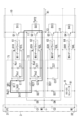
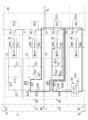
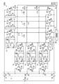
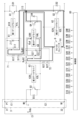
- FIG. 1 is a circuit diagram of a system including a multilevel inverter according to a first embodiment.
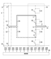
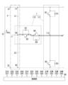
- FIG. 2 is an explanatory diagram of a current path when the switching circuit in the multilevel inverter of the first embodiment is in a first switching state.
- FIG. 3 is an explanatory diagram of a discharge path and a charge path when the switching circuit in the multilevel inverter of the first embodiment is in a first switching state.
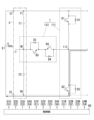
- FIG. 4 is an explanatory diagram of a current path when the switching circuit is in the second switching state in the multilevel inverter of the first embodiment.
- FIG. 5 is an explanatory diagram of a discharge path and a charge path when the switching circuit is in the second switching state in the multilevel inverter of the first embodiment.
- FIG. 6 is an explanatory diagram of a current path when the switching circuit in the multilevel inverter of the first embodiment is in the third switching state.
- FIG. 7 is an explanatory diagram of a discharge path and a charge path when the switching circuit in the multilevel inverter of the first embodiment is in the third switching state.
- FIG. 8 is an explanatory diagram of voltage command values for each phase in the multilevel inverter of the first embodiment.
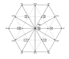
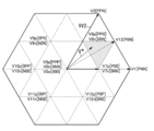
- FIG. 9 is an explanatory diagram of a group of voltage vectors related to the multilevel inverter of the first embodiment.
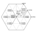
- FIG. 10 is a more detailed illustration of a group of voltage vectors for the multilevel inverter of the first embodiment.
- FIG. 11 is a vector diagram for explaining the operation of the control unit in the multilevel inverter of the first embodiment.
- FIG. 12 is a diagram showing a time chart of the switching state of each phase of the multilevel inverter of the first embodiment.
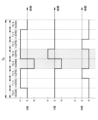
- FIG. 13 is a diagram showing a time chart of the on/off states of the first to fourth switching elements of the multilevel inverter of the first embodiment.
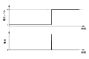
- FIG. 14A is a timing chart showing the relationship between a control signal to a switching element and a current flowing through a control terminal of the switching element when the switching element is turned on.
- FIG. 14B is a timing chart showing the relationship between a control signal to a switching element and a current flowing through a control terminal of the switching element when the switching element is turned off.
- FIG. 15A is a characteristic diagram showing the carrier frequency dependence of the voltage change of a capacitor included in a bootstrap circuit.
- FIG. 15B is a characteristic diagram showing the capacitance dependency of the voltage change of the capacitor included in the bootstrap circuit.
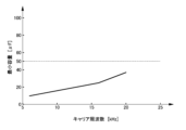
- FIG. 16 is a graph showing the relationship between the minimum capacitance of the capacitor included in the bootstrap circuit, the carrier frequency, and the multi-level vector control (MLVC) ratio.
- FIG. 17 is a graph showing the relationship between the minimum capacitance of the capacitor included in the bootstrap circuit and the carrier frequency.
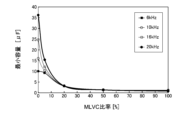
- FIG. 18 is a graph showing the relationship between the minimum capacitance of the capacitor included in the bootstrap circuit and the multilevel vector control ratio.
- FIG. 19A is an explanatory diagram of command voltage vectors and first voltage vectors related to a multilevel inverter according to a comparative example.
- FIG. 19B is an explanatory diagram of a command voltage vector, a zero vector, and a second voltage vector for the multilevel inverter of the comparative example.
- FIG. 20 is a diagram showing a time chart of the switching state of each phase when the inverter circuit of each phase is controlled by replacing the first voltage vector with a zero vector and a second voltage vector in a multilevel inverter of a comparative example.
- FIG. 21 is a diagram showing a time chart of the on/off states of the first to fourth switching elements when the inverter circuit is controlled by replacing the first voltage vector with a zero vector and a second voltage vector in a multilevel inverter of a comparative example.
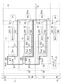
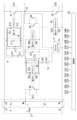
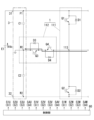
- FIG. 22 is a circuit diagram of a system including a multilevel inverter according to the second embodiment.
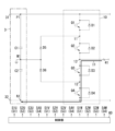
- FIG. 23 is an explanatory diagram of a current path when the switching circuit is in the first switching state in the multilevel inverter of the second embodiment.
- FIG. 24 is an explanatory diagram of a discharge path when the switching circuit is in the first switching state in the multilevel inverter of the second embodiment.
- FIG. 25 is an explanatory diagram of a current path when the switching circuit is in the second switching state in the multilevel inverter of the second embodiment.
- FIG. 26 is an explanatory diagram of a discharge path when the switching circuit is in the second switching state in the multilevel inverter of the second embodiment.
- FIG. 27 is an explanatory diagram of a current path when the switching circuit in the multilevel inverter of the second embodiment is in the third switching state.
- FIG. 24 is an explanatory diagram of a discharge path when the switching circuit is in the first switching state in the multilevel inverter of the second embodiment.
- FIG. 25 is an explanatory diagram of a current path when the switching circuit is in the second switching state in the
- FIG. 28 is an explanatory diagram of a discharge path and a charge path when the switching circuit in the multilevel inverter of the second embodiment is in the third switching state.
- FIG. 29 is an explanatory diagram of a current path when the switching circuit is in the second switching state in the multilevel inverter of the second embodiment.
- FIG. 1 is a circuit diagram of a system including a multilevel inverter 100 according to a first embodiment.
- the multilevel inverter 100 includes a DC power supply unit 3, a plurality of (three in the example of FIG. 1) inverter circuits 1, and a control device 6.
- the DC power supply unit 3 has a positive electrode P1, a negative electrode N1, and an intermediate potential point M1.
- the plurality of inverter circuits 1 are connected between the positive electrode P1 and the negative electrode N1 of the DC power supply unit 3.
- the control device 6 controls the plurality of inverter circuits 1.
- the "intermediate potential point M1" is a point at an intermediate potential between the potential of the positive electrode P1 and the potential of the negative electrode N1 of the DC power supply unit 3.
- the multilevel inverter 100 is a three-level, three-phase inverter of a diode clamp type.
- each of the multiple inverter circuits 1 has an output terminal 41.
- an AC load RA1 is connected to multiple (three in the example of FIG. 1) output terminals 41.
- the AC load RA1 is, for example, a three-phase servo motor.
- one of the multiple inverter circuits 1 is an inverter circuit 1U that outputs a U-phase voltage, another is an inverter circuit 1V that outputs a V-phase voltage, and the remaining one is an inverter circuit 1W that outputs a W-phase voltage.
- Each of the multiple inverter circuits 1 has a switching circuit 10, a first diode D1, a second diode D2, a third diode D3, and a fourth diode D4.
- Each of the multiple inverter circuits 1 also has a first clamp diode D5 and a second clamp diode D6. In the multilevel inverter 100, the potential of the intermediate potential point M1 is clamped by the first clamp diode D5 and the second clamp diode D6 of each inverter circuit 1.
- the first switching element Q1, the second switching element Q2, the third switching element Q3, and the fourth switching element Q4 are connected in series from the positive pole P1 side to the negative pole N1 side of the DC power supply unit 3 in the order of the first switching element Q1, the second switching element Q2, the third switching element Q3, and the fourth switching element Q4.
- the first diode D1 is connected in anti-parallel to the first switching element Q1.
- the second diode D2 is connected in anti-parallel to the second switching element Q2.
- the third diode D3 is connected in anti-parallel to the third switching element Q3.
- the fourth diode D4 is connected in anti-parallel to the fourth switching element Q4.
- the first clamp diode D5 has a cathode connected to the first connection point 11 between the first switching element Q1 and the second switching element Q2, and an anode connected to the intermediate potential point M1.
- the second clamp diode D6 has an anode connected to the second connection point 12 between the third switching element Q3 and the fourth switching element Q4, and a cathode connected to the intermediate potential point M1.
- the control device 6 has a plurality of first gate drivers 61 (three in the example of FIG. 1), a plurality of second gate drivers 62 (three in the example of FIG. 1), a plurality of third gate drivers 63 (three in the example of FIG. 1), and a plurality of fourth gate drivers 64 (three in the example of FIG. 1).
- the control device 6 also has a plurality of bootstrap circuits 71 (three in the example of FIG. 1), a plurality of second bootstrap circuits 72 (three in the example of FIG. 1), a plurality of third bootstrap circuits 73 (three in the example of FIG. 1), a power supply unit 9, and a control unit 60.
- the multiple first gate drivers 61 drive the first switching element Q1 of each of the multiple inverter circuits 1.
- the multiple second gate drivers 62 drive the second switching element Q2 of each of the multiple inverter circuits 1.
- the multiple third gate drivers 63 drive the third switching element Q3 of each of the multiple inverter circuits 1.
- the multiple fourth gate drivers 64 drive the fourth switching element Q4 of each of the multiple inverter circuits 1.
- the multiple first bootstrap circuits 71 correspond one-to-one to the multiple first gate drivers 61. Each of the multiple first bootstrap circuits 71 supplies a voltage to the corresponding first gate driver 61.
- the multiple second bootstrap circuits 72 correspond one-to-one to the multiple second gate drivers 62. Each of the multiple second bootstrap circuits 72 supplies a voltage to the corresponding second gate driver 62.
- the multiple third bootstrap circuits 73 correspond one-to-one to the multiple third gate drivers 63. Each of the multiple third bootstrap circuits 73 supplies a voltage to the corresponding third gate driver 63.
- the power supply unit 9 supplies a voltage to the multiple fourth gate drivers 64.
- the control unit 60 controls a plurality of first gate drivers 61, a plurality of second gate drivers 62, a plurality of third gate drivers 63, and a plurality of fourth gate drivers 64.
- the DC power supply unit 3 has a first capacitor C1 and a second capacitor C2.
- the first capacitor C1 and the second capacitor C2 are connected in series.
- the DC power supply unit 3 further has a first DC terminal 31 connected to the positive pole P1 and a second DC terminal 32 connected to the negative pole N1.
- a first end of the first capacitor C1 is connected to the first DC terminal 31
- a second end of the first capacitor C1 is connected to the first end of the second capacitor C2, and a second end of the second capacitor C2 is connected to the second DC terminal 32.
- a connection point between the first capacitor C1 and the second capacitor C2 is an intermediate potential point M1.
- a DC voltage source E1 is connected between the first DC terminal 31 and the second DC terminal 32.
- the output voltage Vdc of the DC voltage source E1 is applied between the positive electrode P1 and the negative electrode N1 of the DC power supply unit 3.
- the capacitance of the second capacitor C2 is the same as the capacitance of the first capacitor C1.
- the capacitance of the second capacitor C2 is the same as the capacitance of the first capacitor C1
- the switching circuit 10 included in inverter circuit 1U may be referred to as switching circuit 10U
- the switching circuit 10 included in inverter circuit 1V may be referred to as switching circuit 10V
- the switching circuit 10 included in inverter circuit 1W may be referred to as switching circuit 10W
- the output terminal 41 included in inverter circuit 1U may be referred to as output terminal 41U
- the output terminal 41 included in inverter circuit 1V may be referred to as output terminal 41V
- the output terminal included in inverter circuit 1W may be referred to as output terminal 41W.
- the first switching element Q1, the second switching element Q2, the third switching element Q3, and the fourth switching element Q4 of each switching circuit 10 have a control terminal, a first main terminal, and a second main terminal.
- the first switching element Q1, the second switching element Q2, the third switching element Q3, and the fourth switching element Q4 of each switching circuit 10 are, for example, insulated gate bipolar transistors (IGBTs). Therefore, the control terminal, the first main terminal, and the second main terminal of each of the first switching element Q1, the second switching element Q2, the third switching element Q3, and the fourth switching element Q4 of each switching circuit 10 are the gate terminal, the collector terminal, and the emitter terminal, respectively.
- IGBTs insulated gate bipolar transistors
- the control terminal of the first switching element Q1 of each switching circuit 10 is connected to a corresponding first gate driver 61 of the multiple first gate drivers 61.
- the control terminal of the second switching element Q2 of each switching circuit 10 is connected to a corresponding second gate driver 62 of the multiple second gate drivers 62.
- the control terminal of the third switching element Q3 of each switching circuit 10 is connected to a corresponding third gate driver 63 of the multiple third gate drivers 63.
- the control terminal of the fourth switching element Q4 of each switching circuit 10 is connected to a corresponding fourth gate driver 64 of the multiple fourth gate drivers 64.
- the first main terminal of the first switching element Q1 is connected to the positive pole P1 of the DC power supply unit 3, and the second main terminal of the first switching element Q1 is connected to the first main terminal of the second switching element Q2. Also, in each switching circuit 10, the second main terminal of the second switching element Q2 is connected to the first main terminal of the third switching element Q3. Also, in each switching circuit 10, the second main terminal of the third switching element Q3 is connected to the first main terminal of the fourth switching element Q4, and the second main terminal of the fourth switching element Q4 is connected to the negative pole N1 of the DC power supply unit 3.
- the third connection point 13 between the second switching element Q2 and the third switching element Q3 in the switching circuit 10U is connected to the output terminal 41U.
- the third connection point 13 between the second switching element Q2 and the third switching element Q3 in the switching circuit 10V is connected to the output terminal 41V.
- the third connection point 13 between the second switching element Q2 and the third switching element Q3 in the switching circuit 10W is connected to the output terminal 41W.
- the third connection point 13 of the inverter circuit 1U is connected to, for example, the U phase of the AC load RA1 via the output terminal 41U.
- the third connection point 13 of the inverter circuit 1V is connected to, for example, the V phase of the AC load RA1 via the output terminal 41V.
- the third connection point 13 of the inverter circuit 1W is connected to, for example, the W phase of the AC load RA1 via the output terminal 41W.
- the anode of the first diode D1 is connected to the second main terminal (emitter terminal) of the first switching element Q1, and the cathode of the first diode D1 is connected to the first main terminal (collector terminal) of the first switching element Q1.
- the anode of the second diode D2 is connected to the second main terminal (emitter terminal) of the second switching element Q2, and the cathode of the second diode D2 is connected to the first main terminal (collector terminal) of the second switching element Q2.
- the anode of the third diode D3 is connected to the second main terminal (emitter terminal) of the third switching element Q3, and the cathode of the third diode D3 is connected to the first main terminal (collector terminal) of the third switching element Q3.
- the anode of the fourth diode D4 is connected to the second main terminal (emitter terminal) of the fourth switching element Q4, and the cathode of the fourth diode D4 is connected to the first main terminal (collector terminal) of the fourth switching element Q4.
- the first diode D1 may be replaced by a parasitic diode of the IGBT that constitutes the first switching element Q1.
- the second diode D2 may be replaced by a parasitic diode of the IGBT that constitutes the second switching element Q2.
- the third diode D3 may be replaced by a parasitic diode of the IGBT that constitutes the third switching element Q3.
- the fourth diode D4 may be replaced by a parasitic diode of the IGBT that constitutes the fourth switching element Q4.
- the cathode of the first clamp diode D5 is connected to the first connection point 11 between the first switching element Q1 and the second switching element Q2.
- the anode of the first clamp diode D5 is connected to the intermediate potential point M1 of the DC power supply unit 3.
- the intermediate potential point M1 is connected to ground, so the potential of the intermediate potential point M1 is 0V.
- the potential of the positive electrode P1 is Vdc/2
- the potential of the negative electrode N1 is -Vdc/2.
- the cathode of the second clamp diode D6 is connected to the intermediate potential point M1.
- the anode of the second clamp diode D6 is connected to the second connection point 12 between the third switching element Q3 and the fourth switching element Q4.
- the multiple first gate drivers 61 correspond one-to-one to the multiple first switching elements Q1. Each of the multiple first gate drivers 61 is connected to a control terminal of the corresponding first switching element Q1. Each of the multiple first gate drivers 61 drives the corresponding first switching element Q1.
- the multiple first gate drivers 61 are connected to the control unit 60.
- the control unit 60 outputs multiple first control signals S1 (see FIG. 2) that correspond one-to-one to the multiple first gate drivers 61.
- Each of the multiple first gate drivers 61 controls the on/off of the first switching element Q1 based on the given first control signal S1.
- the second gate drivers 62 correspond one-to-one to the second switching elements Q2. Each of the second gate drivers 62 is connected to a control terminal of the corresponding second switching element Q2. Each of the second gate drivers 62 drives the corresponding second switching element Q2.
- the second gate drivers 62 are connected to the control unit 60.
- the control unit 60 outputs second control signals S2 (see FIG. 2) that correspond one-to-one to the second gate drivers 62.
- Each of the second gate drivers 62 controls the on/off of the second switching element Q2 based on the second control signal S2 provided.
- the multiple third gate drivers 63 correspond one-to-one to the multiple third switching elements Q3. Each of the multiple third gate drivers 63 is connected to the control terminal of the corresponding third switching element Q3. Each of the multiple third gate drivers 63 drives the corresponding third switching element Q3.
- the multiple third gate drivers 63 are connected to the control unit 60.
- the control unit 60 outputs multiple third control signals S3 (see FIG. 2) that correspond one-to-one to the multiple third gate drivers 63.
- Each of the multiple third gate drivers 63 controls the on/off of the third switching element Q3 based on the provided third control signal S3.
- the multiple fourth gate drivers 64 correspond one-to-one to the multiple fourth switching elements Q4. Each of the multiple fourth gate drivers 64 is connected to the control terminal of the corresponding fourth switching element Q4. Each of the multiple fourth gate drivers 64 drives the corresponding fourth switching element Q4.
- the multiple fourth gate drivers 64 are connected to the control unit 60.
- the control unit 60 outputs multiple fourth control signals S4 (see FIG. 2) that correspond one-to-one to the multiple fourth gate drivers 64.
- Each of the multiple fourth gate drivers 64 controls the on/off of the fourth switching element Q4 based on the provided fourth control signal S4.
- the first bootstrap circuits 71 correspond one-to-one to the first gate drivers 61. Each of the first bootstrap circuits 71 supplies a voltage to a corresponding one of the first gate drivers 61. Each of the first bootstrap circuits 71 has a diode D17, a resistor R17, and a capacitor C17 (also called a boost capacitor C17). In each of the first bootstrap circuits 71, the anode of the diode D17 is connected to the positive terminal of the power supply unit 9 via the diodes D27 and D37, and the cathode of the diode D17 is connected to the first end of the capacitor C17 via the resistor R17.
- the first end of the capacitor C17 is connected to the high potential side power supply terminal 61H (see FIG. 3) of the first gate driver 61, and the second end of the capacitor C17 is connected to the low potential side power supply terminal 61L (see FIG. 3) of the first gate driver 61.
- the first bootstrap circuit 71 supplies the first gate driver 61 with a voltage required to turn on the first switching element Q1 in the first gate driver 61.
- Each of the first bootstrap circuits 71 further includes a Zener diode Z17 connected in parallel to the capacitor C17.
- the second bootstrap circuits 72 correspond one-to-one to the second gate drivers 62. Each of the second bootstrap circuits 72 supplies a voltage to a corresponding second gate driver 62 among the second gate drivers 62.
- Each of the second bootstrap circuits 72 has a diode D27, a resistor R27, and a capacitor C27 (also called a boost capacitor C27).
- the anode of the diode D27 is connected to the positive terminal of the power supply unit 9 via a diode D37, and the cathode of the diode D27 is connected to a first end of the capacitor C27 via a resistor R27.
- the first end of the capacitor C27 is connected to the high potential side power supply terminal 62H (see FIG.
- the second bootstrap circuit 72 supplies the second gate driver 62 with a voltage required to turn on the second switching element Q2 in the second gate driver 62.
- Each of the second bootstrap circuits 72 further includes a Zener diode Z27 connected in parallel to the capacitor C27.
- the third bootstrap circuits 73 correspond one-to-one to the third gate drivers 63. Each of the third bootstrap circuits 73 supplies a voltage to a corresponding third gate driver 63 among the third gate drivers 63.
- Each of the third bootstrap circuits 73 has a diode D37, a resistor R37, and a capacitor C37 (also called a boost capacitor C37).
- the anode of the diode D37 is connected to the positive terminal of the power supply unit 9, and the cathode of the diode D37 is connected to a first end of the capacitor C37 via the resistor R37.
- the first end of the capacitor C37 is connected to the high potential side power supply terminal 63H (see FIG.
- the third bootstrap circuit 73 supplies the third gate driver 63 with a voltage required to turn on the third switching element Q3 in the third gate driver 63.
- Each of the multiple third bootstrap circuits 73 further includes a Zener diode Z37 connected in parallel to the capacitor C37.
- the power supply unit 9 supplies voltage to the multiple (three) first bootstrap circuits 71, the multiple (three) second bootstrap circuits 72, the multiple (three) third bootstrap circuits 73, and the multiple (three) fourth gate drivers 64.
- the power supply unit 9 is, for example, a DC power supply including an isolated DC-DC converter 91.
- the positive terminal of the power supply unit 9 is connected to the high potential power supply terminal 64H (see FIG. 3) of each of the multiple fourth gate drivers 64, and the negative terminal of the power supply unit 9 is connected to the low potential power supply terminal 64L (see FIG. 3) of each of the multiple fourth gate drivers 64.
- the control unit 60 controls a plurality of first gate drivers 61, a plurality of second gate drivers 62, a plurality of third gate drivers 63, and a plurality of fourth gate drivers 64.
- the control unit 60 controls a plurality of first switching elements Q1, a plurality of second switching elements Q2, a plurality of third switching elements Q3, and a plurality of fourth switching elements Q4.
- the execution subject of the control unit 60 includes a computer system.
- the computer system has one or more computers.
- the computer system is mainly composed of a processor and a memory as hardware.
- the processor executes a program recorded in the memory of the computer system, thereby realizing the function of the control unit 60 as the execution subject in this disclosure.
- the program may be pre-recorded in the memory of the computer system, or may be provided through an electric communication line, or may be recorded and provided on a non-transitory recording medium such as a memory card, an optical disk, or a hard disk drive (magnetic disk) that can be read by the computer system.
- the processor of the computer system is composed of one or more electronic circuits including a semiconductor integrated circuit (IC) or a large-scale integrated circuit (LSI).
- the multiple electronic circuits may be integrated into one chip, or may be distributed across multiple chips.
- the multiple chips may be integrated into one device, or may be distributed across multiple devices.
- the control unit 60 outputs a plurality (three) of first control signals S1 (see FIG. 2) for controlling a plurality (three) of first switching elements Q1, a plurality (three) of second control signals S2 (see FIG. 2) for controlling a plurality (three) of second switching elements Q2, a plurality (three) of third control signals S3 (see FIG. 2) for controlling a plurality (three) of third switching elements Q3, and a plurality (three) of fourth control signals S4 (see FIG. 2) for controlling a plurality (three) of fourth switching elements Q4.
- FIG. 2 shows only one inverter circuit 1 of the three inverter circuits 1 (see FIG. 1), and the remaining two inverter circuits 1 are not shown.
- the first gate drivers 61, the second gate drivers 62, the third gate drivers 63, the fourth gate drivers 64, the first bootstrap circuits 71, the second bootstrap circuits 72, the third bootstrap circuits 73, and the power supply unit 9 shown in FIG. 1 are omitted.
- FIG. 3 only one inverter circuit 1 of the three inverter circuits 1 (see FIG. 1) is shown, and the remaining two inverter circuits 1 are omitted.
- the two first gate drivers 61, the two second gate drivers 62, the two third gate drivers 63, the two fourth gate drivers 64, the two first bootstrap circuits 71, the two second bootstrap circuits 72, and the two third bootstrap circuits 73 shown in FIG. 1 are omitted.
- the three first control signals S1 include a first control signal S1U that controls the first switching element Q1 of the switching circuit 10U, a first control signal S1V that controls the first switching element Q1 of the switching circuit 10V, and a first control signal S1W that controls the first switching element Q1 of the switching circuit 10W.
- the three second control signals S2 include a second control signal S2U that controls the second switching element Q2 of the switching circuit 10U, a second control signal S2V that controls the second switching element Q2 of the switching circuit 10V, and a second control signal S2W that controls the second switching element Q2 of the switching circuit 10W.
- the three third control signals S3 include a third control signal S3U that controls the third switching element Q3 of the switching circuit 10U, a third control signal S3V that controls the third switching element Q3 of the switching circuit 10V, and a third control signal S3W that controls the third switching element Q3 of the switching circuit 10W.
- the three fourth control signals S4 include a fourth control signal S4U that controls the fourth switching element Q4 of the switching circuit 10U, a fourth control signal S4V that controls the fourth switching element Q4 of the switching circuit 10V, and a fourth control signal S4W that controls the fourth switching element Q4 of the switching circuit 10W.
- Each of the multiple first control signals S1, multiple second control signals S2, multiple third control signals S3, and multiple fourth control signals S4 is, for example, a signal whose potential level changes between a first potential level (hereinafter also referred to as a low level) and a second potential level (hereinafter also referred to as a high level) that is higher than the first potential level.
- the first potential level is, for example, 0V
- the second potential level is a potential level greater than the gate threshold voltage of the IGBT. That is, for each of the multiple control signals (multiple first control signals S1, multiple second control signals S2, multiple third control signals S3, and multiple fourth control signals S4), the first potential level is a potential level for turning off the switching element corresponding to that control signal, and the second potential level is a potential level for turning on the switching element corresponding to that control signal.
- Each of the multiple first switching elements Q1 is turned on when the corresponding first control signal S1 is at a high level, and turned off when it is at a low level.
- Each of the multiple second switching elements Q2 is turned on when the corresponding second control signal S2 is at a high level, and turned off when it is at a low level.
- Each of the multiple third switching elements Q3 is turned on when the corresponding third control signal S3 is at a high level, and turned off when it is at a low level.
- Each of the multiple fourth switching elements Q4 is turned on when the corresponding fourth control signal S4 is at a high level, and turned off when it is at a low level.
- each of the multiple inverter circuits 1 is controlled to a first switching state, a second switching state, or a third switching state. That is, in the multilevel inverter 100, the switching state of the switching circuit 10 in each of the three inverter circuits 1U, 1V, and 1W is controlled to one of a first switching state, a second switching state, and a third switching state.
- the first switching state, the second switching state, and the third switching state have different combinations of on/off states of the first to fourth switching elements Q1 to Q4.
- the output voltage in the first switching state, the output voltage in the second switching state, and the output voltage in the third switching state are different from each other.
- the potential level of the output voltage changes in three levels depending on the state of the first to fourth switching elements Q1 to Q4.
- the output voltage of the U-phase inverter circuit 1U, the output voltage of the V-phase inverter circuit 1V, and the output voltage of the W-phase inverter circuit 1W are in different phases from each other.
- the first switching state is a combination in which both the first switching element Q1 and the second switching element Q2 are in the on state, and both the third switching element Q3 and the fourth switching element Q4 are in the off state.
- each of the multiple inverter circuits 1 can output an output voltage at the potential level of the positive electrode P1 of the DC power supply unit 3.
- each of the multiple inverter circuits 1 has the potential of the third connection point 13 at the potential level of the positive electrode P1 of the DC power supply unit 3 (e.g., Vdc/2).
- the second switching state is a combination in which both the first switching element Q1 and the fourth switching element Q4 are in the off state, and both the second switching element Q2 and the third switching element Q3 are in the on state.
- each of the multiple inverter circuits 1 can output an output voltage at the potential level of the intermediate potential point M1 of the DC power supply unit 3.
- the potential of the third connection point 13 becomes the potential level of the intermediate potential point M1 (e.g., 0).
- the third switching state is a combination in which both the first switching element Q1 and the second switching element Q2 are in the off state, and both the third switching element Q3 and the fourth switching element Q4 are in the on state.
- each of the multiple inverter circuits 1 can output an output voltage at the potential level of the negative electrode N1 of the DC power supply unit 3.
- each of the multiple inverter circuits 1 has the potential of the third connection point 13 at the potential level of the negative electrode N1 of the DC power supply unit 3 (for example, -Vdc/2).
- FIG 2 is an explanatory diagram of the current path when the switching circuit 10 is in the first switching state in the multilevel inverter 100 of embodiment 1.
- a current I1 flows through the path from the positive electrode P1 of the DC power supply unit 3 - the first switching element Q1 - the second switching element Q2 - the third connection point 13 - the output terminal 41, and the voltage value of the output voltage to the AC load RA1 (see Figure 1) becomes approximately Vdc/2.
- the switching circuit 10 of the inverter circuit 1 when the switching circuit 10 of the inverter circuit 1 is in the first switching state, the voltage required for the first gate driver 61 to turn on the first switching element Q1 is supplied from the capacitor C17 of the first bootstrap circuit 71 to the first gate driver 61. Therefore, as shown in FIG. 3, the charge in the capacitor C17 of the first bootstrap circuit 71 is discharged through a discharge path Ru1 that is capacitor C17-high potential side power supply terminal 61H of the first gate driver 61-low potential side power supply terminal 61L of the first gate driver 61-capacitor C17. As a result, in the first bootstrap circuit 71, the voltage across the capacitor C17 decreases over time.
- the switching circuit 10 of the inverter circuit 1 when the switching circuit 10 of the inverter circuit 1 is in the first switching state, the voltage required for the second gate driver 62 to turn on the second switching element Q2 is supplied from the capacitor C27 of the second bootstrap circuit 72 to the second gate driver 62. Therefore, the charge in the capacitor C27 of the second bootstrap circuit 72 is discharged via the discharge path Ru2 from the capacitor C27 to the high potential side power supply terminal 62H of the second gate driver 62 to the low potential side power supply terminal 62L of the second gate driver 62 to the capacitor C27. As a result, in the second bootstrap circuit 72, the voltage across the capacitor C27 decreases over time.
- FIG. 3 is an explanatory diagram of the discharge path and the charge path when the switching circuit 10 is in the first switching state in the multilevel inverter 100 of the first embodiment.
- the capacitor C17 is charged by the capacitor C27 if the first condition is satisfied.
- the voltages across the capacitor C17 are Vo1, Vo2, Vd1, VR1, and Vf2, respectively, the voltages across the diode D17, resistor R17, and second switching element Q2 are Vf2, the first condition is Vo2>(Vo1+Vd1+VR1+Vf2).
- the charge path Ru21 for charging the capacitor C17 by the capacitor C27 is the path of the capacitor C27-resistor R27-diode D17-resistor R17-capacitor C17-first connection point 11-second switching element Q2-capacitor C27.
- FIG. 4 is an explanatory diagram of a current path when the switching circuit 10 is in the second switching state in the multilevel inverter 100 of the first embodiment.
- the switching circuit 10 of the inverter circuit 1 When the switching circuit 10 of the inverter circuit 1 is in the second switching state and the polarity of the output current is positive, as shown in FIG. 4, the current I1 flows through the path (path indicated by the thick solid arrow) of the intermediate potential point M1 of the DC power supply unit 3-the first clamp diode D5-the second switching element Q2-the third connection point 13-the output terminal 41, and the voltage value of the output voltage to the AC load RA1 becomes 0.
- the current I1 flows through the path of the intermediate potential point M1 of the DC power supply unit 3-the first clamp diode D5 of the inverter circuit 1U-the second switching element Q2 of the switching circuit 10U-the third connection point 13-the output terminal 41.
- the switching circuit 10 of the inverter circuit 1 when the switching circuit 10 of the inverter circuit 1 is in the second switching state and the polarity of the output current is negative, as shown in FIG. 4, the current I1 flows through the path (path indicated by the thick dashed arrow) of the output terminal 41-the third connection point 13-the third switching element Q3-the second connection point 12-the second clamp diode D6, and the voltage value of the output voltage to the AC load RA1 becomes 0.
- the switching circuits 10U, 10V, and 10W are in the second switching state, the second switching state, and the first switching state, respectively, in the inverter circuit 1U, the current I1 flows through the path (path indicated by the thick dashed arrow) of the output terminal 41-the third connection point 13-the third switching element Q3-the second connection point 12-the second clamp diode D6, and the voltage value of the output voltage to the AC load RA1 becomes 0.
- FIG. 5 is an explanatory diagram of the discharge path and the charge path when the switching circuit 10 is in the second switching state in the multilevel inverter 100 of the first embodiment.
- the switching circuit 10 of the inverter circuit 1 When the switching circuit 10 of the inverter circuit 1 is in the second switching state, the voltage required to turn on the second switching element Q2 is supplied from the capacitor C27 of the second bootstrap circuit 72 to the second gate driver 62 by the second gate driver 62. Therefore, the charge of the capacitor C27 of the second bootstrap circuit 72 is discharged through the discharge path Ru2 of the capacitor C27-the high potential side power supply terminal 62H of the second gate driver 62-the low potential side power supply terminal 62L of the second gate driver 62-the capacitor C27, as shown in FIG. 5.
- the switching circuit 10 of the inverter circuit 1 when the switching circuit 10 of the inverter circuit 1 is in the second switching state, the voltage required to turn on the third switching element Q3 is supplied from the capacitor C37 of the third bootstrap circuit 73 to the third gate driver 63 by the third gate driver 63. Therefore, the charge in the capacitor C37 of the third bootstrap circuit 73 is discharged through the discharge path Ru3 from the capacitor C37 to the high potential side power supply terminal 63H of the third gate driver 63 to the low potential side power supply terminal 63L of the third gate driver 63 to the capacitor C37.
- the capacitor C27 is charged by the capacitor C37 if the second condition is met, and the capacitor C17 is charged by the capacitor C27 if the third condition is met.
- the voltages across the capacitors C17, C27, and C37 are Vo1, Vo2, and Vo3, respectively, the voltages across the diodes D17 and D27 are Vd1 and Vd2, respectively, the voltages across the resistors R17 and R27 are VR1 and VR2, respectively, and the voltages across the second switching element Q2 and the third switching element Q3 are Vf2 and Vf3, respectively, the second condition is Vo3>(Vo2+Vd2+VR2+Vf3).
- the third condition is Vo2>(Vo1+Vd1+VR1+Vf2).
- the charging path Ru32 that charges the capacitor C27 with the capacitor C37 is the path of the capacitor C37-resistor R37-diode D27-resistor R27-capacitor C27-third connection point 13-third switching element Q3-capacitor C37.
- the charging path Ru21 that charges the capacitor C17 with the capacitor C27 is the path of the capacitor C27-resistor R27-diode D17-resistor R17-capacitor C17-first connection point 11-second switching element Q2-capacitor C27.
- FIG. 6 is an explanatory diagram of a current path when the switching circuit 10 is in the third switching state in the multilevel inverter 100 of embodiment 1.
- a current I1 flows through a path from the output terminal 41-the third connection point 13-the third switching element Q3-the fourth switching element Q4-the negative pole N1 of the DC power supply unit 3, and the voltage value of the output voltage to the AC load RA1 becomes -Vdc/2.
- the capacitor C27 of the second bootstrap circuit 72 see FIG.
- the capacitor C37 of the third bootstrap circuit 73 supplies the third gate driver 63 with a voltage required to turn on the third switching element Q3 by the third gate driver 63. Therefore, the charge of the capacitor C37 of the third bootstrap circuit 73 is discharged through a discharge path Ru3 that is capacitor C37-high potential side power supply terminal 63H of the third gate driver 63-low potential side power supply terminal 63L of the third gate driver 63-capacitor C37. Also, when the switching circuit 10 of the inverter circuit 1 is in the third switching state, the capacitor C37 is charged by the power supply unit 9 when the fourth condition is met, and the capacitor C27 is charged by the capacitor C37 when the fifth condition is met.
- the fourth condition is Voo>(Vo3+Vd3+VR3+Vf4).
- the fifth condition is Vo3>(Vo2+Vd2+VR2+Vf3).
- the charging path Ru93 which charges the capacitor C37 from the power supply unit 9, is a path from the positive terminal of the power supply unit 9 to the diode D37 to the resistor R37 to the capacitor C37 to the second connection point 12 to the fourth switching element Q4 to the negative terminal of the power supply unit 9.
- the charging path Ru32 which charges the capacitor C27 from the capacitor C37, is a path from the capacitor C37 to the resistor R37 to the diode D27 to the resistor R27 to the capacitor C27 to the third connection point 13 to the third switching element Q3 to the capacitor C37.
- the control unit 60 generates first to fourth control signals S1 to S4 (S1U to S4U) for the first to fourth switching elements Q1 to Q4 of the inverter circuit 1U, first to fourth control signals S1 to S4 (S1V to S4V) for the first to fourth switching elements Q1 to Q4 of the inverter circuit 1V, and first to fourth control signals S1 to S4 (S1W to S4W) for the first to fourth switching elements Q1 to Q4 of the inverter circuit 1W, based on the voltage commands Vu, Vv, and Vw (see FIG. 8) related to the output voltages of the inverter circuits 1U, 1V, and 1W, respectively.
- the control unit 60 may perform PI (Proportional Integral) control of the voltage commands Vu, Vv, and Vw based on information output from the detection unit 8 that detects the state of the AC load RA1.
- PI Proportional Integral
- the information output from the detection unit 8 includes, for example, at least one of the following: information on the detection results of a plurality of current sensors that detect the output currents flowing through the U-phase, V-phase, and W-phase of the AC load RA1; and information on the detection results of an encoder that detects the rotation speed, rotation angle, etc. of the three-phase motor.
- one of the three inverter circuits 1 (for example, the U-phase inverter circuit 1U) will be described.
- the operation of the V-phase inverter circuit 1V and the W-phase inverter circuit 1W is similar to that of the U-phase inverter circuit 1U.
- the output voltages of the U-phase inverter circuit 1U, the V-phase inverter circuit 1V, and the W-phase inverter circuit 1W are out of phase with each other.
- the control unit 60 controls a plurality of first gate drivers 61, a plurality of second gate drivers 62, a plurality of third gate drivers 63, and a plurality of fourth gate drivers 64 by performing voltage vector control.
- the voltage vector control by the control unit 60 is explained in more detail below.
- the control unit 60 stores a group of voltage vectors in advance.
- Each of the group of voltage vectors is determined by a combination of the potential levels of the connection point (third connection point 13) between the second switching element Q2 and the third switching element Q3 of the multiple inverter circuits 1.
- the group of voltage vectors is determined by the switching state of the switching circuit 10U corresponding to the U phase, the switching state of the switching circuit 10V corresponding to the V phase, and the switching state of the switching circuit 10W corresponding to the W phase.
- the group of voltage vectors includes three zero vectors V0p, V0n, and V0o, each of which has a magnitude of zero.
- the group of voltage vectors also includes six voltage vectors V1, V2, V3, V4, V5, and V6, each of which has a magnitude of (2/3)1/2 ⁇ 2 Vdc and has different directions.
- the group of voltage vectors also includes 12 voltage vectors V7p, V7n, V8p, V8n, V9p, V9n, V10p, V10n, V11p, V11n, V12p, and V12n, each of which has a magnitude of (2/3)1/2 ⁇ Vdc.
- the group of voltage vectors includes six voltage vectors V13, V14, V15, V16, V17, and V18, each of which has a magnitude of (2/3)1/2 ⁇ 31/2 ⁇ Vdc and a different direction.
- the angle between two adjacent voltage vectors among the six voltage vectors V1, V2, V3, V4, V5, and V6 is 60 degrees.
- the angle between two adjacent voltage vectors among the six voltage vectors V13, V14, V15, V16, V17, and V18 is also 60 degrees.
- FIG. 9 is a vector diagram illustrating the group of voltage vectors on an orthogonal d-q coordinate system.
- the group of voltage vectors can be expressed as shown in Figure 10 by expressing the first switching state, the second switching state, and the third switching state with the symbols "P", “0", and “N”, respectively, and listing the U phase, V phase, and W phase in that order.
- V0p[PPP] expresses that, with respect to the zero vector V0p, the switching state of the U-phase switching circuit 10U is "P", the switching state of the V-phase switching circuit 10V is "P”, and the switching state of the W-phase switching circuit 10W is "P".
- a voltage vector with "p" attached, such as V10p includes "P” and does not include "N”.
- a voltage vector with "n” attached, such as V10n includes “N” and does not include “P”.
- voltage vectors with “o” attached, such as V10o include “0” and do not include “P” or “N”.
- V1, V2, V3, V4, V5, and V6 can be expressed as V1[PNN], V2[PPN], V3[NPN], V4[NPP], V5[NNP], and V6[PNP], respectively.
- Voltage vectors that do not have "p,” "n,” or "o” added after the number added to "V,” such as V1[PNN], V2[PPN], V3[NPN], V4[NPP], V5[NNP], and V6[PNP] include "P" and "N” as the switching states of the three phases.
- the 12 voltage vectors V7p, V7n, V8p, V8n, V9p, V9n, V10p, V10n, V11p, V11n, V12p, and V12n can be expressed as V7p[P00], V7n[0NN], V8p[PP0], V8n[00N], V9p[0P0], V9n[N0N], V10p[0PP], V10n[N00], V11p[00P], V11n[NN0], V12p[P0P], and V12n[0N0], respectively.
- V13, V14, V15, V16, V17, and V18 can be expressed as V13[P0N], V14[0PN], V15[NP0], V16[N0P], V17[0NP], and V18[PN0], respectively.
- the control unit 60 converts the instantaneous value of the command voltage for the output voltage of each of the multiple inverter circuits 1 into a command voltage vector V* (see FIG. 11). If the d-axis component of the command voltage vector V* on the orthogonal d-q coordinate system is Vd and the q-axis component of the command voltage vector V* on the orthogonal d-q coordinate system is Vq, the command voltage vector V* can be calculated using equation (1).
- the control unit 60 selects a plurality of (e.g., five) voltage vectors adjacent to the command voltage vector V* from the group of voltage vectors.
- FIG. 11 is a vector diagram for explaining the operation of the control unit 60 in the multilevel inverter 100 of the first embodiment.
- the plurality of voltage vectors are V8p[PP0], V8n[00N], V13[P0N], V7p[P00], and V7n[0NN].
- the angle between the voltage vector closest to the command voltage vector V* (hereinafter also referred to as voltage vector VV1) and the command voltage vector V* is less than 30 degrees.
- the control unit 60 within a given control period Ts, matches the resultant vector of the vectors of the vertices of an equilateral triangle surrounding the command voltage vector V* with the command voltage vector V*. That is, the control unit 60 matches the resultant vector of the voltage vector VV1 (V8p[PP0] and V8n[00N] in the example of FIG. 11), the voltage vector V13[P0N], and the voltage vectors V7p[P00] and V7n[0NN] with the command voltage vector V*.
- the control period Ts is one period of the carrier signal.
- the switching state of only one of the U, V, and W phases in two voltage vectors arranged in time series changes between "P" and "0” or between "0” and “N", and the same voltage vector is output twice.
- the voltage vector V8n[00N] ⁇ voltage vector V13[P0N] ⁇ voltage vector V7p[P00] ⁇ voltage vector V8p[PP0] ⁇ voltage vector V8p[PP0] ⁇ voltage vector V7p[P00] ⁇ voltage vector V13[P0N] ⁇ voltage vector V8n[00N] are output in this order.
- the voltage vector Va is the voltage vector V8p[PP0] and V8n[00N]
- the voltage vector Vb is the voltage vector V13[P0N]
- the voltage vector Vc is the voltage vector V7p[P00] and V7n[0NN].
- FIG. 12 is a diagram showing a time chart of the switching state of each phase of the multilevel inverter 100 of embodiment 1.
- the on/off states of the first switching element Q1, the second switching element Q2, the third switching element Q3, and the fourth switching element Q4 are as shown in FIG. 13 within the control period Ts.
- FIG. 13 is a diagram showing a time chart of the on/off states of the first to fourth switching elements (Q1 to Q4) of the multilevel inverter 100 of embodiment 1.
- the second switching element Q2 is in the on state for the entire period within the control period Ts, and the voltage drop width of the second bootstrap circuit 72 becomes large.
- the order of the voltage vectors within the control period Ts may differ depending on the initial value of the carrier signal at the start of the control period Ts.
- FIG. 14A is a timing chart showing the relationship between the control signal to the switching elements (Q1 to Q4) when the switching elements (Q1 to Q4) are turned on and the current flowing through the control terminal of the switching elements (Q1 to Q4).
- the multilevel inverter 100 when the potential level of the control signal S1 to each of the multiple first switching elements Q1 changes from a low level ("L" in FIG. 14A) to a high level ("H" in FIG. 14A), a pulsed current (see FIG. 14A) flows through the control terminal of the first switching element Q1 that is turned on. This consumes the charge of the capacitor C17 of the bootstrap circuit 71 that corresponds to the first switching element Q1 that is turned on among the multiple bootstrap circuits 71.
- FIG. 14B is a timing chart showing the relationship between the control signal to the switching elements (Q1 to Q4) and the current flowing through the control terminal of the switching elements (Q1 to Q4) when the switching elements (Q1 to Q4) are turned off.
- a pulsed current flows through the control terminal of the first switching element Q1 that is turned off. This consumes the charge of the capacitor C17 of the bootstrap circuit 71 that corresponds to the first switching element Q1 that is turned on among the multiple bootstrap circuits 71.
- the carrier frequency is the frequency of the carrier signal that is determined by the period of the carrier signal.
- FIG. 15A is a diagram showing the carrier frequency dependence of the voltage change of capacitor C17 in the multilevel inverter 100 of embodiment 1.
- FIG. 15A shows the time change of the voltage of capacitor C17 (the voltage Vo1 across both ends described above) when the carrier frequency is changed with the capacitance of capacitor C17 set to 0.2 ⁇ F.
- “A1” shows the time change of the voltage of capacitor C17 when the carrier frequency is set to 6 kHz
- “A2” shows the time change of the voltage of capacitor C17 when the carrier frequency is set to 12 kHz
- “A3” shows the time change of the voltage of capacitor C17 when the carrier frequency is set to 20 kHz.
- FIG. 15B is a diagram showing the capacitance dependency of the voltage change of capacitor C17 in the multilevel inverter 100 of embodiment 1. It shows the time change of the voltage of capacitor C17 when the carrier frequency is set to 20 kHz and the capacitance of capacitor C17 is changed.
- "A4" shows the time change of the voltage of capacitor C17 when the capacitance of capacitor C17 is set to 0.2 ⁇ F
- "A5" shows the time change of the voltage of capacitor C17 when the capacitance of capacitor C17 is set to 1 ⁇ F
- “A6” shows the time change of the voltage of capacitor C17 when the capacitance of capacitor C17 is set to 10 ⁇ F.
- the capacitance of each of the capacitors C17 in the multiple first bootstrap circuits 71 is set to a value of 10 ⁇ F or more and 50 ⁇ F or less.
- the capacitance of each of the capacitors C27 in the multiple second bootstrap circuits 72 is set to a value of 10 ⁇ F or more and 50 ⁇ F or less.
- the capacitance of each of the capacitors C37 in the multiple third bootstrap circuits 73 is set to a value of 10 ⁇ F or more and 50 ⁇ F or less.
- the capacitance of each of the capacitors C17, C27, and C37 is set, for example, according to the value of the carrier frequency. How to determine the capacitance of each of the capacitors C17, C27, and C37 will be explained with reference to Figures 16 to 18 after explaining the operation of the control unit of the multilevel inverter according to the comparative example with reference to Figures 19A, 19B, 20, and 21.
- a control unit performs control to replace some voltage vectors with other voltage vectors in voltage vector control.
- the control unit selects multiple (e.g., five) voltage vectors that are adjacent to the command voltage vector V* (see FIG. 19A) from the group of voltage vectors.
- FIG. 19A is an explanatory diagram of the command voltage vector and the first voltage vector for a multilevel inverter according to a comparative example.
- the multiple voltage vectors are V8p[PP0], V8n[00N], V13[P0N], V7p[P00], and V7n[0NN].
- the control unit replaces one of the two first voltage vectors VV1 (V8p[PP0] and V8n[00N] in the example of FIG. 19A), which are the two voltage vectors VV1 whose magnitude is a reference magnitude and closest to the command voltage vector V*, with a zero vector V0n[NNN] in which the potential level of the third connection point 13 of the multiple inverter circuits 1 is a negative potential, and at least one second voltage vector VV2 (V2[PPN] in the example of FIG. 19A) that has the same direction as the first voltage vector VV1 but a different magnitude from the first voltage vector VV1.
- the reference magnitude is, for example, (2/3)1/2 ⁇ Vdc.
- the multiple voltage vectors include 12 voltage vectors V7p[P00], V7n[0NN], V8p[PP0], V8n[00N], V9p[0P0], V9n[N0N], V10p[0PP], V10n[N00], V11p[00P], V11n[NN0], V12p[P0P], and V12n[0N0] as voltage vectors whose magnitude is a reference magnitude (reference vectors).
- the angle between the command voltage vector V* and the two first voltage vectors VV1 closest to the command voltage vector V* is less than 30 degrees.
- FIG. 19B is an explanatory diagram of a command voltage vector, a zero vector, and a second voltage vector for a multilevel inverter of a comparative example.
- the control unit controls the first gate drivers, the second gate drivers, the third gate drivers, and the fourth gate drivers within a predetermined control period Ts (see FIG. 20) so that the composite vector of three voltage vectors (V13[P0N], V7p[P00], and V7n[0NN] in the example of FIG. 19B) other than the first voltage vector VV1 (V8p[PP0] and V8n[00N] in the example of FIG. 19A), the zero vector V0n[NNN], and at least one second voltage vector VV2 coincides with the command voltage vector V*.
- the predetermined control period Ts is, for example, two periods of the carrier signal.
- FIG. 20 is a diagram showing a time chart of the switching state of each phase when the inverter circuit of each phase is controlled by replacing the first voltage vector with a zero vector and a second voltage vector in a multilevel inverter of a comparative example.
- the on/off of the first switching element Q1, the second switching element Q2, the third switching element Q3, and the fourth switching element Q4 is as shown in FIG. 21 within a control period Ts.
- FIG. 21 is a diagram showing a time chart of the on/off state of the first to fourth switching elements when the inverter circuit is controlled by replacing the first voltage vector with a zero vector and a second voltage vector in a multilevel inverter of a comparative example.
- control unit may replace the first voltage vector VV1 with the zero vector V0n [NNN] and the second voltage vector VV2 only when the polarity of the command voltage corresponding to the command voltage vector V* is positive, and may also replace the first voltage vector VV1 with the zero vector V0n [NNN] and the second voltage vector VV2 when the polarity of the command voltage is negative.
- FIG. 16 is a graph showing the results of a simulation of the relationship between the minimum capacitance of the capacitor C17 included in the first bootstrap circuit 71, the carrier frequency, and the multilevel vector control (MLVC) ratio.
- the "minimum capacitance” means the lower limit of the capacitance of the capacitor C17 required to maintain the voltage value of the gate voltage required to turn on and off the first switching element Q1 in the capacitor C17.
- the "MLVC ratio" indicates the ratio at which the voltage vector control of the comparative example is performed relative to the voltage vector control of the first embodiment, and when the value of the MLVC ratio is 0, it means that only the voltage vector control of the first embodiment is performed, and the voltage vector control of the comparative example is not performed. In addition, the greater the value of the MLVC ratio is than 0, the higher the frequency of replacing the voltage vector in the voltage vector control of the comparative example.
- the defined plane PL1 surrounded by a thick line is a plane that defines the minimum capacitance of capacitor C17 required to maintain the gate voltage value (e.g., 11 V) required to turn the first switching element Q1 on and off in capacitor C17. Therefore, if the capacitance of capacitor C17 is greater than the minimum capacitance of any point of the combination of carrier frequency and MLVC ratio in FIG. 16 projected vertically onto defined plane PL1, it becomes possible to maintain the gate voltage value required to turn the first switching element Q1 on and off in capacitor C17.
- the gate voltage value e.g. 11 V
- FIG. 17 is a graph showing the results of a simulation of the relationship between the minimum capacitance of capacitor C17 included in the first bootstrap circuit 71 and the carrier frequency. It can be seen from FIG. 17 that the minimum capacitance of capacitor C17 increases as the carrier frequency increases. Note that FIG. 17 is a graph for the case in FIG. 16 where the HLVC ratio is 0%.
- Figure 18 is a graph showing the relationship between the minimum capacitance of capacitor C17 included in the first bootstrap circuit 71 and the MLVC ratio.
- Figure 18 shows the relationship between the minimum capacitance of capacitor C17 and the MLVC ratio when the carrier frequency in Figure 16 is 6 kHz, 10 kHz, 16 kHz, and 20 kHz. It can be seen from Figure 18 that the minimum capacitance of capacitor C17 increases as the carrier frequency increases. It can also be seen from Figure 18 that the minimum capacitance of capacitor C17 can be reduced by increasing the MLVC ratio.
- the upper limit of the minimum capacitance of each of the capacitors C17 in the first bootstrap circuits 71 is preferably 50 ⁇ F, from the viewpoint of using a capacitor smaller than an aluminum electrolytic capacitor as the capacitor C17. Therefore, it is preferable that the capacitance of each of the capacitors C17 in the first bootstrap circuits 71 is 10 ⁇ F or more and 50 ⁇ F or less.
- the capacitor C17 of each of the multiple first bootstrap circuits 71 is, for example, a multilayer ceramic capacitor, a film capacitor, or a tantalum electrolytic capacitor.
- the minimum capacitance of each of the capacitors C17 in the multiple first bootstrap circuits 71 has been described above, but the same applies to the minimum capacitance of each of the capacitors C27 in the multiple second bootstrap circuits 72 and the minimum capacitance of each of the capacitors C37 in the multiple third bootstrap circuits 73.
- the capacitance of the capacitor C17 included in each of the first bootstrap circuits 71 is not less than 10 ⁇ F and not more than 50 ⁇ F.
- the control unit 60 can maintain the voltage of the capacitor C17 of the multiple first bootstrap circuits 71 at or above the voltage required to turn the first switching element Q1 on and off without performing special voltage vector control to replace the voltage vector.
- the capacitance of the capacitor C27 included in each of the second bootstrap circuits 72 is 10 ⁇ F or more and 50 ⁇ F or less.
- the above configuration makes it possible to suppress the voltage drop of the capacitor C27 of the second bootstrap circuit 72.
- the capacitance of the capacitor C37 included in each of the third bootstrap circuits 73 is 10 ⁇ F or more and 50 ⁇ F or less.
- the above configuration makes it possible to suppress the voltage drop of the capacitor C37 of the third bootstrap circuit 73.
- the DC-DC converter 91 included in the power supply unit 9 supplies voltage to the multiple fourth gate drivers 64 and the multiple third bootstrap circuits 73. This makes it possible for the multilevel inverter 100 according to the first embodiment to suppress voltage drops in each of the multiple third bootstrap circuits 73 while achieving miniaturization.
- the multilevel inverter 100A includes, for example, a DC power supply unit 3, a plurality of (three in the example of Fig. 22) inverter circuits 1, and a control device 6, as shown in Fig. 22.
- the DC power supply unit 3 has a positive electrode P1, a negative electrode N1, and an intermediate potential point M1.
- the plurality of inverter circuits 1 are connected between the positive electrode P1 and the negative electrode N1 of the DC power supply unit 3.
- the control device 6 controls the plurality of inverter circuits 1.
- the multilevel inverter 100A is a T-type three-level three-phase inverter.
- each of the multiple inverter circuits 1 has an output terminal 41.
- an AC load RA1 is connected to multiple (three in the example of FIG. 22) output terminals (AC terminals) 41.
- the AC load RA1 is, for example, a three-phase servo motor.
- one of the multiple inverter circuits 1 is an inverter circuit 1U that outputs a U-phase voltage
- another is an inverter circuit 1V that outputs a V-phase voltage
- the remaining one is an inverter circuit 1W that outputs a W-phase voltage.
- Each of the multiple inverter circuits 1 has a first switching element Q1, a second switching element Q2, a third switching element Q3, and a fourth switching element Q4, and a first diode D1, a second diode D2, a third diode D3, and a fourth diode D4.
- the first diode D1, the second diode D2, the third diode D3, and the fourth diode D4 are connected in anti-parallel to the first switching element Q1, the second switching element Q2, the third switching element Q3, and the fourth switching element Q4, respectively.
- the first switching element Q1 and the second switching element Q2 are connected in series from the positive pole P1 side to the negative pole N1 side in the order of the first switching element Q1 and the second switching element Q2.
- a series circuit (first circuit 111) of the first switching element Q1 and the second switching element Q2 is connected between the positive pole P1 and the negative pole N1.
- a series circuit (second circuit 112) of a third switching element Q3 and a fourth switching element Q4 is connected between an intermediate potential point M1 and an output point.
- the output point is a connection point 113 between the first switching element Q1 and the second switching element Q2.
- the second circuit 112 has a bidirectional switch including the third switching element Q3, the fourth switching element Q4, the third diode D3, and the fourth diode D4.
- the control device 6 has a plurality of first gate drivers 61 (three in the example of FIG. 22), a plurality of second gate drivers 62 (three in the example of FIG. 22), a plurality of third gate drivers 63 (three in the example of FIG. 22), and a plurality of fourth gate drivers 64 (three in the example of FIG. 22).
- the control device 6 also has a plurality of bootstrap circuits 71 (hereinafter also referred to as first bootstrap circuits 71) (three in the example of FIG. 22), a plurality of second bootstrap circuits 72 (three in the example of FIG. 22), a power supply unit 9, and a control unit 60.
- the multiple first gate drivers 61 drive the first switching elements Q1 of the multiple inverter circuits 1.
- the multiple second gate drivers 62 drive the second switching elements Q2 of the multiple inverter circuits 1.
- the multiple third gate drivers 63 drive the third switching elements Q3 of the multiple inverter circuits 1.
- the multiple fourth gate drivers 64 drive the fourth switching elements Q4 of the multiple inverter circuits 1.
- the multiple first bootstrap circuits 71 correspond one-to-one to the multiple first gate drivers 61. Each of the multiple first bootstrap circuits 71 supplies a voltage to a corresponding first gate driver 61 among the multiple first gate drivers 61.
- the multiple second bootstrap circuits 72 correspond to the multiple third gate drivers 63 and the multiple fourth gate drivers 64. Each of the multiple second bootstrap circuits 72 supplies a voltage to a corresponding third gate driver 63 and a corresponding fourth gate driver 64 among the multiple third gate drivers 63.
- the power supply unit 9 supplies a voltage to the multiple second gate drivers 62.
- the control unit 60 controls a plurality of first gate drivers 61, a plurality of second gate drivers 62, a plurality of third gate drivers 63, and a plurality of fourth gate drivers 64.
- the DC power supply unit 3 has a first capacitor C1 and a second capacitor C2.
- the first capacitor C1 and the second capacitor C2 are connected in series.
- a first end of the first capacitor C1 is connected to a first DC terminal 31
- a second end of the first capacitor C1 is connected to a first end of the second capacitor C2
- a second end of the second capacitor C2 is connected to a second DC terminal 32.
- a connection point between the first capacitor C1 and the second capacitor C2 is an intermediate potential point M1.
- the DC power supply unit 3 further has a first DC terminal 31 connected to a positive pole P1 and a second DC terminal 32 connected to a negative pole N1.
- a DC voltage source E1 is connected between the first DC terminal 31 and the second DC terminal 32.
- the output voltage Vdc of the DC voltage source E1 is applied between the positive electrode P1 and the negative electrode N1 of the DC power supply unit 3.
- the capacitance of the second capacitor C2 is the same as the capacitance of the first capacitor C1.
- the capacitance of the second capacitor C2 is the same as the capacitance of the first capacitor C1
- the output terminal 41 included in the inverter circuit 1U among the multiple output terminals 41 may be referred to as the output terminal 41U
- the output terminal 41 included in the inverter circuit 1V may be referred to as the output terminal 41V
- the output terminal included in the inverter circuit 1W may be referred to as the output terminal 41W.
- the first switching element Q1, the second switching element Q2, the third switching element Q3, and the fourth switching element Q4 of each inverter circuit 1 have a control terminal, a first main terminal, and a second main terminal.
- the first switching element Q1, the second switching element Q2, the third switching element Q3, and the fourth switching element Q4 of each inverter circuit 1 are, for example, IGBTs. Therefore, the control terminal, the first main terminal, and the second main terminal of each of the first switching element Q1, the second switching element Q2, the third switching element Q3, and the fourth switching element Q4 of each inverter circuit 1 are the gate terminal, the collector terminal, and the emitter terminal, respectively.
- the control terminal of the first switching element Q1 of each inverter circuit 1 is connected to a corresponding first gate driver 61 of the multiple first gate drivers 61. Also, the control terminal of the second switching element Q2 of each inverter circuit 1 is connected to a corresponding second gate driver 62 of the multiple second gate drivers 62. Also, the control terminal of the third switching element Q3 of each inverter circuit 1 is connected to a corresponding third gate driver 63 of the multiple third gate drivers 63. Also, the control terminal of the fourth switching element Q4 of each inverter circuit 1 is connected to a corresponding fourth gate driver 64 of the multiple fourth gate drivers 64.
- the first main terminal of the first switching element Q1 is connected to the positive pole P1 of the DC power supply unit 3
- the second main terminal of the first switching element Q1 is connected to the first main terminal of the second switching element Q2
- the second main terminal of the second switching element Q2 is connected to the negative pole N1 of the DC power supply unit 3.
- the bidirectional switch of the second circuit 112 is a common emitter bidirectional switch in which the second main terminals (emitter terminals) of the third switching element Q3 and the fourth switching element Q4 are connected to each other.
- the "intermediate potential point M1" is a point that is an intermediate potential between the potential of the positive electrode P1 and the potential of the negative electrode N1 of the DC power supply unit 3.
- the potential of the intermediate potential point M1 is 0V.
- the potential of the positive electrode P1 is Vdc/2
- the potential of the negative electrode N1 is -Vdc/2.
- connection point 113 between the first switching element Q1 and the second switching element Q2 is connected to the output terminal 41U.
- the connection point 113 between the first switching element Q1 and the second switching element Q2 is connected to the output terminal 41V.
- connection point 113 between the first switching element Q1 and the second switching element Q2 is connected to the output terminal 41W.
- the connection point 113 of the inverter circuit 1U is connected to, for example, the U phase of the AC load RA1 via the output terminal 41U.
- the connection point 113 of the inverter circuit 1V is connected to, for example, the V phase of the AC load RA1 via the output terminal 41V.
- the connection point 113 of the inverter circuit 1W is connected to, for example, the W phase of the AC load RA1 via the output terminal 41W.
- the anode of the first diode D1 is connected to the second main terminal (emitter terminal) of the first switching element Q1, and the cathode of the first diode D1 is connected to the first main terminal (collector terminal) of the first switching element Q1.
- the anode of the second diode D2 is connected to the second main terminal (emitter terminal) of the second switching element Q2, and the cathode of the second diode D2 is connected to the first main terminal (collector terminal) of the second switching element Q2.
- the anode of the third diode D3 is connected to the second main terminal (emitter terminal) of the third switching element Q3, and the cathode of the third diode D3 is connected to the first main terminal (collector terminal) of the third switching element Q3.
- the anode of the fourth diode D4 is connected to the second main terminal (emitter terminal) of the fourth switching element Q4, and the cathode of the fourth diode D4 is connected to the first main terminal (collector terminal) of the fourth switching element Q4.
- the first diode D1 may be replaced by a parasitic diode of the IGBT that constitutes the first switching element Q1.
- the second diode D2 may be replaced by a parasitic diode of the IGBT that constitutes the second switching element Q2.
- the third diode D3 may be replaced by a parasitic diode of the IGBT that constitutes the third switching element Q3.
- the fourth diode D4 may be replaced by a parasitic diode of the IGBT that constitutes the fourth switching element Q4.
- the multiple first gate drivers 61 correspond one-to-one to the multiple first switching elements Q1. Each of the multiple first gate drivers 61 is connected to a control terminal of a corresponding first switching element Q1 among the multiple first switching elements Q1. The multiple first gate drivers 61 drive the corresponding first switching element Q1. The multiple first gate drivers 61 are connected to a control unit 60. The control unit 60 outputs multiple first control signals S1 (see FIG. 23) that correspond one-to-one to the multiple first gate drivers 61. Each of the multiple first gate drivers 61 controls the on/off of the first switching element Q1 based on the given first control signal S1.
- the second gate drivers 62 correspond one-to-one to the second switching elements Q2. Each of the second gate drivers 62 is connected to a control terminal of a corresponding one of the second switching elements Q2. The second gate drivers 62 drive the corresponding second switching element Q2. The second gate drivers 62 are connected to the control unit 60.
- the control unit 60 outputs second control signals S2 (see FIG. 23) that correspond one-to-one to the second gate drivers 62.
- Each of the second gate drivers 62 controls the on/off of the second switching element Q2 based on the second control signal S2 provided.
- the multiple third gate drivers 63 correspond one-to-one to the multiple third switching elements Q3.
- Each of the multiple third gate drivers 63 is connected to a control terminal of a corresponding one of the multiple third switching elements Q3.
- the multiple third gate drivers 63 drive the corresponding third switching element Q3.
- the multiple third gate drivers 63 are connected to the control unit 60.
- the control unit 60 outputs multiple third control signals S3 (see FIG. 2) that correspond one-to-one to the multiple third gate drivers 63.
- Each of the multiple third gate drivers 63 controls the on/off of the third switching element Q3 based on the provided third control signal S3.
- the multiple fourth gate drivers 64 correspond one-to-one to the multiple fourth switching elements Q4. Each of the multiple fourth gate drivers 64 is connected to a control terminal of a corresponding one of the multiple fourth switching elements Q4. The multiple fourth gate drivers 64 drive the corresponding fourth switching element Q4. The multiple fourth gate drivers 64 are connected to the control unit 60.
- the control unit 60 outputs multiple fourth control signals S4 (see FIG. 23) that correspond one-to-one to the multiple fourth gate drivers 64.
- Each of the multiple fourth gate drivers 64 controls the on/off of the fourth switching element Q4 based on the provided fourth control signal S4.
- the first bootstrap circuits 71 correspond one-to-one to the first gate drivers 61.
- the first bootstrap circuits 71 supply voltages to the corresponding first gate drivers 61.
- each of the first bootstrap circuits 71 has a diode D17, a resistor R17, and a capacitor C17 (also called a boost capacitor C17).
- the anode of the diode D17 is connected to the positive terminal of the power supply unit 9, and the cathode of the diode D17 is connected to a first end of the capacitor C17 via the resistor R17.
- the first end of the capacitor C17 is connected to the high-potential power supply terminal 61H (see FIG.
- the first bootstrap circuit 71 supplies the first gate driver 61 with a voltage required to turn on the first switching element Q1 in the first gate driver 61.
- Each of the first bootstrap circuits 71 further includes a Zener diode Z17 connected in parallel to the capacitor C17.
- the multiple second bootstrap circuits 72 correspond to the multiple third gate drivers 63 and the multiple fourth gate drivers 64.
- the multiple second bootstrap circuits 72 supply voltages to the corresponding third gate drivers 63 and the corresponding fourth gate drivers 64.
- Each of the multiple second bootstrap circuits 72 has a diode D27, a resistor R27, and a capacitor C27 (also referred to as a boost capacitor C27).
- the anode of the diode D27 is connected to the positive terminal of the power supply unit 9, and the cathode of the diode D27 is connected to a first end of the capacitor C27 via the resistor R27.
- the first end of the capacitor C27 is connected to the high potential side power supply terminal 63H (see FIG.
- the second bootstrap circuit 72 supplies the third gate driver 63 with a voltage required to turn on the third switching element Q3 in the third gate driver 63, and supplies the fourth gate driver 64 with a voltage required to turn on the fourth switching element Q4 in the fourth gate driver 64.
- Each of the second bootstrap circuits 72 further includes a Zener diode Z27 connected in parallel to the capacitor C27.
- the power supply unit 9 supplies voltage to a plurality of (three in the example of FIG. 22) first bootstrap circuits 71, a plurality of (three in the example of FIG. 22) second bootstrap circuits 72, and a plurality of (three in the example of FIG. 22) second gate drivers 62.
- the power supply unit 9 is, for example, a DC power supply including an isolated DC-DC converter 91.
- the positive terminal of the power supply unit 9 is connected to the high potential power supply terminal 62H (see FIG. 24) of each of the second gate drivers 62, and the negative terminal of the power supply unit 9 is connected to the low potential power supply terminal 62L (see FIG. 24) of each of the second gate drivers 62.
- the control unit 60 controls a plurality of first gate drivers 61, a plurality of second gate drivers 62, a plurality of third gate drivers 63, and a plurality of fourth gate drivers 64.
- the control unit 60 controls a plurality of first switching elements Q1, a plurality of second switching elements Q2, a plurality of third switching elements Q3, and a plurality of fourth switching elements Q4.
- the execution subject of the control unit 60 includes a computer system.
- the computer system has one or more computers.
- the computer system is mainly composed of a processor and a memory as hardware.
- the processor executes a program recorded in the memory of the computer system, thereby realizing the function of the control unit 60 as the execution subject in this disclosure.
- the program may be pre-recorded in the memory of the computer system, or may be provided through an electric communication line, or may be recorded and provided on a non-transitory recording medium such as a memory card, an optical disk, or a hard disk drive (magnetic disk) that can be read by the computer system.
- the processor of the computer system is composed of one or more electronic circuits including a semiconductor integrated circuit (IC) or a large-scale integrated circuit (LSI).
- the multiple electronic circuits may be integrated into one chip, or may be distributed across multiple chips.
- the multiple chips may be integrated into one device, or may be distributed across multiple devices.
- the control unit 60 outputs a plurality (three) of first control signals S1 (see FIG. 23) for controlling a plurality (three) of first switching elements Q1, a plurality (three) of second control signals S2 (see FIG. 23) for controlling a plurality (three) of second switching elements Q2, a plurality (three) of third control signals S3 (see FIG. 23) for controlling a plurality (three) of third switching elements Q3, and a plurality (three) of fourth control signals S4 (see FIG. 23) for controlling a plurality (three) of fourth switching elements Q4.
- first control signals S1 see FIG. 23
- second control signals S2 for controlling a plurality (three) of second switching elements Q2
- a plurality (three) of third control signals S3 for controlling a plurality (three) of third switching elements Q3
- a plurality (three) of fourth control signals S4 for controlling a plurality (three) of fourth switching elements Q4.
- a plurality of first gate drivers 61, a plurality of second gate drivers 62, a plurality of third gate drivers 63, a plurality of fourth gate drivers 64, a plurality of first bootstrap circuits 71, a plurality of second bootstrap circuits 72, and a power supply unit 9 are omitted from illustration.
- FIG. 24 only one of the three inverter circuits 1 is shown, and the remaining two inverter circuits 1 are omitted.
- the two first gate drivers 61, the two second gate drivers 62, the two third gate drivers 63, the two fourth gate drivers 64, the two first bootstrap circuits 71, and the two second bootstrap circuits 72 are omitted.
- the three first control signals S1 include a first control signal S1U that controls the first switching element Q1 of the inverter circuit 1U, a first control signal S1V that controls the first switching element Q1 of the inverter circuit 1V, and a first control signal S1W that controls the first switching element Q1 of the inverter circuit 1W.
- the three second control signals S2 include a second control signal S2U that controls the second switching element Q2 of the inverter circuit 1U, a second control signal S2V that controls the second switching element Q2 of the inverter circuit 1V, and a second control signal S2W that controls the second switching element Q2 of the inverter circuit 1W.
- the three third control signals S3 include a third control signal S3U that controls the third switching element Q3 of the inverter circuit 1U, a third control signal S3V that controls the third switching element Q3 of the inverter circuit 1V, and a third control signal S3W that controls the third switching element Q3 of the inverter circuit 1W.
- the three fourth control signals S4 include a fourth control signal S4U that controls the fourth switching element Q4 of the inverter circuit 1U, a fourth control signal S4V that controls the fourth switching element Q4 of the inverter circuit 1V, and a fourth control signal S4W that controls the fourth switching element Q4 of the inverter circuit 1W.
- Each of the multiple first control signals S1, multiple second control signals S2, multiple third control signals S3, and multiple fourth control signals S4 is, for example, a signal whose potential level changes between a first potential level (hereinafter also referred to as a low level) and a second potential level (hereinafter also referred to as a high level) that is higher than the first potential level.
- the first potential level is, for example, 0V
- the second potential level is a potential level higher than the gate threshold voltage of the IGBT.
- the first potential level is a potential level for turning off the switching element corresponding to that control signal
- the second potential level is a potential level for turning on the switching element corresponding to that control signal
- Each of the multiple first switching elements Q1 is turned on when the corresponding first control signal S1 is at a high level, and turned off when it is at a low level.
- Each of the multiple second switching elements Q2 is turned on when the corresponding second control signal S2 is at a high level, and turned off when it is at a low level.
- Each of the multiple third switching elements Q3 is turned on when the corresponding third control signal S3 is at a high level, and turned off when it is at a low level.
- Each of the multiple fourth switching elements Q4 is turned on when the corresponding fourth control signal S4 is at a high level, and turned off when it is at a low level.
- each of the multiple inverter circuits 1 is controlled to a first switching state, a second switching state, or a third switching state. That is, in the multilevel inverter 100A, the switching state is controlled to one of the first switching state, the second switching state, and the third switching state in each of the three inverter circuits 1U, 1V, and 1W.
- the first switching state, the second switching state, and the third switching state have different combinations of on/off states of the first to fourth switching elements Q1 to Q4.
- the output voltage in the first switching state, the output voltage in the second switching state, and the output voltage in the third switching state are different from each other.
- the potential level of the output voltage changes in three levels depending on the state of the first to fourth switching elements Q1 to Q4.
- the output voltage of the U-phase inverter circuit 1U, the output voltage of the V-phase inverter circuit 1V, and the output voltage of the W-phase inverter circuit 1W are in different phases from each other.
- the first switching state is a combination in which both the first switching element Q1 and the third switching element Q3 are in the on state, and both the second switching element Q2 and the fourth switching element Q4 are in the off state.
- each of the multiple inverter circuits 1 can output an output voltage at the potential level of the positive electrode P1 of the DC power supply unit 3.
- each of the multiple inverter circuits 1 has the potential of the connection point 113 at the potential level of the positive electrode P1 of the DC power supply unit 3 (e.g., Vdc/2).
- the second switching state is a combination in which both the first switching element Q1 and the second switching element Q2 are in the off state, and both the third switching element Q3 and the fourth switching element Q4 are in the on state.
- each of the multiple inverter circuits 1 can output an output voltage at the potential level of the intermediate potential point M1 of the DC power supply unit 3.
- each of the multiple inverter circuits 1 has the potential of the connection point 113 at the potential level of the intermediate potential point M1 (e.g., 0).
- the third switching state is a combination in which both the first switching element Q1 and the third switching element Q3 are in the off state, and both the second switching element Q2 and the fourth switching element Q4 are in the on state.
- each of the multiple inverter circuits 1 can output an output voltage at the potential level of the negative electrode N1 of the DC power supply unit 3.
- each of the multiple inverter circuits 1 has the potential of the connection point 113 at the potential level of the negative electrode N1 of the DC power supply unit 3 (for example, -Vdc/2).
- Fig. 23 is an explanatory diagram of the current path when the switching circuit is in the first switching state in the multilevel inverter 100A of embodiment 2.
- a current flows through the path from the positive electrode P1 of the DC power supply unit 3 to the first switching element Q1 to the connection point 113 to the output terminal 41, and the voltage value of the output voltage to the AC load RA1 (see Fig. 22) becomes Vdc/2.
- the power supply unit 9 When the inverter circuit 1 is in the first switching state, the power supply unit 9 does not charge the capacitor C17 of the first bootstrap circuit 71, and the first gate driver 61 supplies the voltage required to turn on the first switching element Q1 from the capacitor C17 of the first bootstrap circuit 71 to the first gate driver 61. Therefore, as shown in FIG. 24, the charge in the capacitor C17 of the first bootstrap circuit 71 is discharged through a discharge path Ru1 that is capacitor C17-high potential side power supply terminal 61H of the first gate driver 61-low potential side power supply terminal 61L of the first gate driver 61-capacitor C17. As a result, in the first bootstrap circuit 71, the voltage across the capacitor C17 decreases over time.
- FIG. 24 is an explanatory diagram of a discharge path when the switching circuit is in the first switching state in the multilevel inverter 100A of the second embodiment.
- the power supply unit 9 does not charge the capacitor C27 of the second bootstrap circuit 72, and the third gate driver 63 supplies the voltage required to turn on the third switching element Q3 from the capacitor C27 of the second bootstrap circuit 72 to the third gate driver 63. Therefore, as shown in FIG. 24, the charge of the capacitor C27 of the second bootstrap circuit 72 is discharged through the discharge path Ru3 of the capacitor C27-the high potential side power supply terminal 63H of the third gate driver 63-the low potential side power supply terminal 63L of the third gate driver 63-the capacitor C27. As a result, in the second bootstrap circuit 72, the voltage across the capacitor C27 decreases over time.
- FIG. 25 is an explanatory diagram of a current path when the switching circuit is in the second switching state in the multilevel inverter 100A of the second embodiment.
- the inverter circuit 1 When the inverter circuit 1 is in the second switching state (when it changes from the first switching state to the second switching state), for example, as shown in FIG. 25, a current flows through the path of the intermediate potential point M1 of the DC power supply unit 3-the third switching element Q3-the fourth switching element Q4-the connection point 113-the output terminal 41 (see FIG. 22), and the voltage value of the output voltage to the AC load RA1 becomes 0.
- 26 is an explanatory diagram of a discharge path when the switching circuit is in the second switching state in the multilevel inverter 100A of embodiment 2.
- a voltage required to turn on the third switching element Q3 is supplied from the capacitor C27 of the second bootstrap circuit 72 to the third gate driver 63 by the third gate driver 63. Therefore, as shown in FIG. 26, the charge of the capacitor C27 of the second bootstrap circuit 72 is discharged through a discharge path Ru3 of the capacitor C27-the high potential side power supply terminal 63H of the third gate driver 63-the low potential side power supply terminal 63L of the third gate driver 63-the capacitor C27.
- the inverter circuit 1 when the inverter circuit 1 is in the second switching state, a voltage required to turn on the fourth switching element Q4 is supplied from the capacitor C27 of the second bootstrap circuit 72 to the fourth gate driver 64 by the fourth gate driver 64. Therefore, the charge in the capacitor C27 of the second bootstrap circuit 72 is discharged through a discharge path Ru4 from the capacitor C27 to the high-potential power supply terminal 64H of the fourth gate driver 64 to the low-potential power supply terminal 64L of the fourth gate driver 64 to the capacitor C27.
- FIG. 27 is an explanatory diagram of the current path when the switching circuit is in the third switching state in the multilevel inverter 100A of the second embodiment.
- the inverter circuit 1 When the inverter circuit 1 is in the third switching state, as shown in FIG. 27, a current flows through the path of the output terminal 41-connection point 113-second switching element Q2-negative pole N1 of the DC power supply unit 3, and the voltage value of the output voltage to the AC load RA1 becomes -Vdc/2.
- the capacitor C17 of the first bootstrap circuit 71 is charged by the power supply unit 9, so that the voltage of the capacitor C17 increases over time and the capacitor C17 becomes fully charged.
- FIG. 28 is an explanatory diagram of the discharge path and charge path when the switching circuit is in the third switching state in the multilevel inverter 100A of embodiment 2.
- the charge path Ru91 for charging the capacitor C17 by the power supply unit 9 is the path from the positive terminal of the power supply unit 9 - diode D17 - resistor R17 - capacitor C17 - connection point 113 - second switching element Q2 - negative terminal of the power supply unit 9.
- the capacitor C27 of the second bootstrap circuit 72 is charged by the power supply unit 9.
- the charging path Ru92 for charging the capacitor C27 by the power supply unit 9 is the path from the positive terminal of the power supply unit 9 - diode D27 - resistor R27 - capacitor C27 - fourth switching element Q4 - connection point 113 - second switching element Q2 - negative terminal of the power supply unit 9.
- FIG. 29 is an explanatory diagram of the current path when the switching circuit is in the second switching state in the multilevel inverter 100A of the second embodiment.
- the inverter circuit 1 When the inverter circuit 1 is in the second switching state (when it changes from the third switching state to the second switching state), for example, as shown in FIG. 29, a current flows through the path of the output terminal 41-connection point 113-fourth switching element Q4-third switching element Q3-mid-potential point M1, and the voltage value of the output voltage to the AC load RA1 becomes 0.
- the control unit 60 generates, for example, first to fourth control signals S1 to S4 (S1U to S4U) for the first to fourth switching elements Q1 to Q4 of the inverter circuit 1U, first to fourth control signals S1 to S4 (S1V to S4V) for the first to fourth switching elements Q1 to Q4 of the inverter circuit 1V, and first to fourth control signals S1 to S4 (S1W to S4W) for the first to fourth switching elements Q1 to Q4 of the inverter circuit 1W, based on the voltage commands Vu, Vv, and Vw (see FIG. 8) related to the output voltages of the inverter circuits 1U, 1V, and 1W, respectively.
- the voltage commands Vu and Vv are sinusoidal signals with a phase difference of, for example, 120°, and their values (voltage command values) change over time.
- the voltage commands Vu, Vv, and Vw have the same length of one cycle.
- the control unit 60 may perform PI (Proportional Integral) control of the voltage commands Vu, Vv, and Vw based on information output from a detection unit 8 that detects the state of the AC load RA1.
- PI Proportional Integral
- the information output from the detection unit 8 includes, for example, at least one of the following: information on the detection results of a plurality of current sensors that detect the output currents flowing through the U-phase, V-phase, and W-phase of the AC load RA1; and information on the detection results of an encoder that detects the rotation speed, rotation angle, etc. of the three-phase motor.
- one of the three inverter circuits 1 (for example, the U-phase inverter circuit 1U) will be described.
- the operation of the V-phase inverter circuit 1V and the W-phase inverter circuit 1W is similar to that of the U-phase inverter circuit 1U.
- the output voltages of the U-phase inverter circuit 1U, the V-phase inverter circuit 1V, and the W-phase inverter circuit 1W are out of phase with each other.
- the control unit 60 performs voltage vector control to control the first gate drivers 61, the second gate drivers 62, the third gate drivers 63, and the fourth gate drivers 64.
- the control unit 60 performs voltage vector control similar to that of embodiment 1.
- the control unit 60 controls the first gate drivers 61, the second gate drivers 62, the third gate drivers 63, and the fourth gate drivers 64 so that the composite vector of the vectors of the vertices of an equilateral triangle surrounding the command voltage vector V* (see FIG. 11) coincides with the command voltage vector V* within a control period Ts (see FIG. 12 and FIG. 13).
- the method of voltage vector control is the same as that of embodiment 1, so a description thereof will be omitted.
- the cause of the voltage drop in the capacitor C17 of each of the multiple first bootstrap circuits 71 is the same as in embodiment 1.
- the cause of the voltage drop in the capacitor C27 of each of the multiple second bootstrap circuits 72 is also the same as in embodiment 1.
- the upper limit of the minimum capacitance of each of the capacitors C17 in the first bootstrap circuits 71 is preferably 50 ⁇ F, from the viewpoint of using a capacitor smaller than an aluminum electrolytic capacitor as the capacitor C17. Therefore, it is preferable that the capacitance of each of the capacitors C17 in the first bootstrap circuits 71 is 10 ⁇ F or more and 50 ⁇ F or less.
- the capacitor C17 of each of the multiple first bootstrap circuits 71 is, for example, a multilayer ceramic capacitor, a film capacitor, or a tantalum electrolytic capacitor.
- the capacitance of each of the capacitors C17 in the first bootstrap circuits 71 is set to a value greater than or equal to 10 ⁇ F and less than or equal to 50 ⁇ F.
- the capacitance of each of the capacitors C27 in the second bootstrap circuits 72 is set to a value greater than or equal to 10 ⁇ F and less than or equal to 50 ⁇ F.
- the capacitance of the capacitor C17 included in each of the multiple first bootstrap circuits 71 is not less than 10 ⁇ F and not more than 50 ⁇ F.
- the control unit 60 can maintain the voltage of the capacitor C17 of the multiple first bootstrap circuits 71 at or above the voltage required to turn the first switching element Q1 on and off without performing special voltage vector control to replace the voltage vector.
- the capacitance of the capacitor C27 included in each of the second bootstrap circuits 72 is 10 ⁇ F or more and 50 ⁇ F or less.
- the above configuration makes it possible to suppress the voltage drop of the capacitor C27 of the second bootstrap circuit 72.
- each of the first switching elements Q1, the second switching elements Q2, the third switching elements Q3, and the fourth switching elements Q4 may be a MOSFET, not limited to an IGBT.
- the control terminal, the first main terminal, and the second main terminal of each of the first switching elements Q1, the second switching elements Q2, the third switching elements Q3, and the fourth switching elements Q4 are a gate terminal, a drain terminal, and a source terminal, respectively.
- the MOSFET constituting each of the first switching element Q1, the second switching element Q2, the third switching element Q3, and the fourth switching element Q4 is, for example, a normally-off type n-channel MOSFET.
- the MOSFET is a Si-based MOSFET, but is not limited to a Si-based MOSFET and may be, for example, a SiC-based MOSFET.
- each of the multiple first bootstrap circuits 71 includes a Zener diode Z17, but may be configured not to include the Zener diode Z17.
- each of the multiple second bootstrap circuits 72 includes a Zener diode Z27, but may be configured not to include the Zener diode Z27.
- the multilevel inverters 100 and 100A may be multilevel inverters with three or more levels, for example, they may be five-level inverters.
- the multilevel inverter (100; 100A) includes a DC power supply unit (3), a plurality of inverter circuits (1), and a control device (6).
- the DC power supply unit (3) has a positive pole (P1), a negative pole (N1), and an intermediate potential point (M1).
- the plurality of inverter circuits (1) are connected between the positive pole (P1) and the negative pole (N1) of the DC power supply unit (3).
- the control device (6) controls the plurality of inverter circuits (1).
- Each of the plurality of inverter circuits (1) is a neutral point clamped inverter.
- Each of the plurality of inverter circuits (1) has a first switching element (Q1), a second switching element (Q2), a third switching element (Q3), and a fourth switching element (Q4), and a first diode (D1), a second diode (D2), a third diode (D3), and a fourth diode (D4).
- the first diode (D1), the second diode (D2), the third diode (D3), and the fourth diode (D4) are connected in anti-parallel to the first switching element (Q1), the second switching element (Q2), the third switching element (Q3), and the fourth switching element (Q4), respectively.
- the control device (6) has a plurality of first gate drivers (61), a plurality of second gate drivers (62), a plurality of third gate drivers (63), a plurality of fourth gate drivers (64), a plurality of bootstrap circuits (71), a power supply unit (9), and a control unit (60).
- the plurality of first gate drivers (61) drive the first switching elements (Q1) of each of the plurality of inverter circuits (1).
- the plurality of second gate drivers (62) drive the second switching elements (Q2) of each of the plurality of inverter circuits (1).
- the plurality of third gate drivers (63) drive the third switching elements (Q3) of each of the plurality of inverter circuits (1).
- the plurality of fourth gate drivers (64) drive the fourth switching elements (Q4) of each of the plurality of inverter circuits (1).
- the plurality of bootstrap circuits (71) correspond one-to-one to the plurality of first gate drivers (61).
- Each of the plurality of bootstrap circuits (71) supplies a voltage to a corresponding first gate driver (61) among the plurality of first gate drivers (61).
- the power supply unit (9) supplies a voltage to the plurality of bootstrap circuits (71).
- the control unit (60) controls the plurality of first gate drivers (61), the plurality of second gate drivers (62), the plurality of third gate drivers (63), and the plurality of fourth gate drivers (64).
- Each of the plurality of bootstrap circuits (71) includes a capacitor (C17) and a diode (D17) connected in series to the capacitor (C17).
- the capacitance of the capacitor (C17) included in each of the plurality of bootstrap circuits (71) is 10 ⁇ F or more and 50 ⁇ F or less.
- the control unit (60) controls the first gate drivers (61), the second gate drivers (62), the third gate drivers (63), and the fourth gate drivers (64) within a predetermined control period (Ts) so as to match a composite vector of the voltage vectors corresponding to the vertices of an equilateral triangle surrounding the command voltage vector (V*) among the group of voltage vectors with the command voltage vector (V*).
- Ts control period
- Each of the group of voltage vectors is determined by a combination of multiple potential levels in the multiple inverter circuits (1).
- each of the multiple inverter circuits (1) has a first clamp diode (D5) and a second clamp diode (D6).
- D5 first clamp diode
- D6 second clamp diode
- the first switching element (Q1), the second switching element (Q2), the third switching element (Q3), and the fourth switching element (Q4) are connected in series in the order of the first switching element (Q1), the second switching element (Q2), the third switching element (Q3), and the fourth switching element (Q4) from the positive pole (P1) side.
- the cathode of the first clamp diode (D5) is connected to the first connection point (11) between the first switching element (Q1) and the second switching element (Q2), and the anode of the first clamp diode (D5) is connected to the intermediate potential point (M1).
- the anode of the second clamp diode (D6) is connected to the second connection point (12) between the third switching element (Q3) and the fourth switching element (Q4), and the cathode of the second clamp diode (D6) is connected to the intermediate potential point (M1).
- the third connection point (13) between the second switching element (Q2) and the third switching element (Q3) is connected to an output terminal (41) that is connected to an AC load.
- the multilevel inverter (100A) according to the fourth aspect is based on the first or second aspect.
- the first switching element (Q1) and the second switching element (Q2) are connected in series from the positive electrode (P1) side to the negative electrode (N1) side in the order of the first switching element (Q1) and the second switching element (Q2).
- a series circuit of the third switching element (Q3) and the fourth switching element (Q4) is connected between the intermediate potential point (M1) and the output point.
- the output point is the connection point (113) between the first switching element (Q1) and the second switching element.
- the multilevel inverter (100; 100A) according to the fifth aspect is based on any one of the first to fourth aspects.
- the first switching element (Q1), the second switching element (Q2), the third switching element (Q3), and the fourth switching element (Q4) are each an insulated gate bipolar transistor.
- the capacitor (C17) included in each of the multiple bootstrap circuits (71) is a multilayer ceramic capacitor, a film capacitor, or a tantalum electrolytic capacitor.
- the multilevel inverter of the present disclosure is capable of suppressing the voltage drop in the bootstrap circuit. In this way, the multilevel inverter of the present disclosure is industrially useful.
Landscapes
- Engineering & Computer Science (AREA)
- Power Engineering (AREA)
- Inverter Devices (AREA)
Abstract
ブートストラップ回路の電圧低下を抑制する。マルチレベルインバータ(100)は、直流電源部(3)と、複数のインバータ回路(1)と、制御装置(6)と、を備える。複数のインバータ回路(1)の各々は、第1スイッチング素子(Q1)、第2スイッチング素子(Q2)、第3スイッチング素子(Q3)及び第4スイッチング素子(Q4)を有する。制御装置(6)は、複数の第1ゲートドライバ(61)と、複数の第2ゲートドライバ(62)と、複数の第3ゲートドライバ(63)と、複数の第4ゲートドライバ(64)と、複数のブートストラップ回路(71)と、電源部(9)と、制御部(60)と、を有する。マルチレベルインバータ(100)では、複数の第1ブートストラップ回路(71)の各々に含まれるコンデンサ(C17)の容量は、10μF以上かつ50μF以下である。
Description
本開示は、マルチレベルインバータに関し、より詳細には、ブートストラップ回路を備えるマルチレベルインバータに関する。
特許文献1は、3レベル中性点クランプ形インバータのスイッチング素子駆動回路を開示している。
特許文献1に開示された中性点クランプ形インバータは、第1スイッチング素子、第2スイッチング素子、第3スイッチング素子及び第4スイッチング素子の直列回路と、第1クランプダイオードと、第2クランプダイオードと、直流電圧の平滑化及びその中性点電位を生成する、2つの平滑コンデンサの直列回路(直流電源部)と、を備える。
また、スイッチング素子駆動回路は、第1スイッチング素子を駆動するための第1ゲート駆動回路(第1ゲートドライバ)と、第2スイッチング素子を駆動するための第2ゲート駆動回路(第2ゲートドライバ)と、第3スイッチング素子を駆動するための第3ゲート駆動回路(第3ゲートドライバ)と、第4スイッチング素子を駆動するための第4ゲート駆動回路(第4ゲートドライバ)と、を備える。第1ゲート駆動回路、第2ゲート駆動回路、第3ゲート駆動回路及び第4ゲート駆動回路には、制御回路(制御部)によりスイッチング信号が入力される。
また、スイッチング素子駆動回路は、ゲート電源(電源部)を備える。スイッチング素子駆動回路では、第1ゲート駆動回路に対しては、コンデンサが並列に接続されている。コンデンサは、ダイオードを介してゲート電源により充電される。第1スイッチング素子のゲート駆動用電源は、コンデンサに充電された電圧となる。
特許文献1に開示された第1スイッチング素子、第2スイッチング素子、第3スイッチング素子及び第4スイッチング素子のセットを複数備えるマルチレベルインバータでは、コンデンサとダイオードとを含むブートストラップ回路の電圧低下が問題となることがある。
本開示の目的は、ブートストラップ回路の電圧低下を抑制することが可能なマルチレベルインバータを提供することにある。
本開示に係る一態様のマルチレベルインバータは、直流電源部と、複数のインバータ回路と、制御装置と、を備える。前記直流電源部は、正極と負極と中間電位点とを有する。前記複数のインバータ回路は、前記直流電源部の前記正極と前記負極との間に接続されている。前記制御装置は、前記複数のインバータ回路を制御する。前記複数のインバータ回路の各々は、中性点クランプ型インバータである。前記複数のインバータ回路の各々は、第1スイッチング素子、第2スイッチング素子、第3スイッチング素子及び第4スイッチング素子と、第1ダイオード、第2ダイオード、第3ダイオード及び第4ダイオードと、を有する。前記第1ダイオード、前記第2ダイオード、前記第3ダイオード及び前記第4ダイオードは、前記第1スイッチング素子、前記第2スイッチング素子、前記第3スイッチング素子及び前記第4スイッチング素子にそれぞれ逆並列接続されている。前記制御装置は、複数の第1ゲートドライバと、複数の第2ゲートドライバと、複数の第3ゲートドライバと、複数の第4ゲートドライバと、複数のブートストラップ回路と、電源部と、制御部と、を有する。前記複数の第1ゲートドライバは、前記複数のインバータ回路の各々の前記第1スイッチング素子を駆動する。前記複数の第2ゲートドライバは、前記複数のインバータ回路の各々の前記第2スイッチング素子を駆動する。前記複数の第3ゲートドライバは、前記複数のインバータ回路の各々の前記第3スイッチング素子を駆動する。前記複数の第4ゲートドライバは、前記複数のインバータ回路の各々の前記第4スイッチング素子を駆動する。前記複数のブートストラップ回路は、前記複数の第1ゲートドライバに一対一に対応する。前記複数のブートストラップ回路の各々は、前記複数の第1ゲートドライバのうち対応する第1ゲートドライバに電圧を供給する。前記電源部は、前記複数のブートストラップ回路に電圧を供給する。前記制御部は、前記複数の第1ゲートドライバ、前記複数の第2ゲートドライバ、前記複数の第3ゲートドライバ及び前記複数の第4ゲートドライバを制御する。前記複数のブートストラップ回路の各々は、コンデンサと、前記コンデンサに直列接続されているダイオードと、を含む。前記複数のブートストラップ回路の各々に含まれる前記コンデンサの容量は、10μF以上かつ50μF以下である。
本開示のマルチレベルインバータは、ブートストラップ回路の電圧低下を抑制することが可能となるという効果がある。
(実施形態1)
以下では、実施形態1に係るマルチレベルインバータ100について、図1~18に基づいて説明する。
以下では、実施形態1に係るマルチレベルインバータ100について、図1~18に基づいて説明する。
(1)マルチレベルインバータの全体構成
図1は、実施形態1に係るマルチレベルインバータ100を備えるシステムの回路図である。マルチレベルインバータ100は、例えば、図1に示すように、直流電源部3と、複数(図1の例では3つ)のインバータ回路1と、制御装置6と、を備える。直流電源部3は、正極P1と負極N1と中間電位点M1とを有する。複数のインバータ回路1は、直流電源部3の正極P1と負極N1との間に接続されている。制御装置6は、複数のインバータ回路1を制御する。「中間電位点M1」とは、直流電源部3の正極P1の電位と負極N1の電位との間の中間の電位となる点である。
図1は、実施形態1に係るマルチレベルインバータ100を備えるシステムの回路図である。マルチレベルインバータ100は、例えば、図1に示すように、直流電源部3と、複数(図1の例では3つ)のインバータ回路1と、制御装置6と、を備える。直流電源部3は、正極P1と負極N1と中間電位点M1とを有する。複数のインバータ回路1は、直流電源部3の正極P1と負極N1との間に接続されている。制御装置6は、複数のインバータ回路1を制御する。「中間電位点M1」とは、直流電源部3の正極P1の電位と負極N1の電位との間の中間の電位となる点である。
マルチレベルインバータ100は、ダイオードクランプ型の3レベル3相インバータである。マルチレベルインバータ100では、複数のインバータ回路1の各々が出力端子41を有している。マルチレベルインバータ100では、複数(図1の例では3つ)の出力端子41に交流負荷RA1が接続される。
交流負荷RA1は、例えば、3相サーボモータである。マルチレベルインバータ100では、複数のインバータ回路1のうちの1つが、U相の電圧を出力するインバータ回路1Uであり、別の1つが、V相の電圧を出力するインバータ回路1Vであり、残りの1つが、W相の電圧を出力するインバータ回路1Wである。
複数のインバータ回路1の各々は、スイッチング回路10と、第1ダイオードD1と、第2ダイオードD2と、第3ダイオードD3と、第4ダイオードD4と、を有する。また、複数のインバータ回路1の各々は、第1クランプダイオードD5と、第2クランプダイオードD6と、を有する。マルチレベルインバータ100では、中間電位点M1の電位が、各インバータ回路1の第1クランプダイオードD5及び第2クランプダイオードD6によってクランプされる。
各スイッチング回路10では、第1スイッチング素子Q1、第2スイッチング素子Q2、第3スイッチング素子Q3及び第4スイッチング素子Q4が、直流電源部3の正極P1側から負極N1側へ第1スイッチング素子Q1、第2スイッチング素子Q2、第3スイッチング素子Q3及び第4スイッチング素子Q4の順に並ぶように直列接続されている。
各インバータ回路1では、第1ダイオードD1は、第1スイッチング素子Q1に逆並列接続されている。第2ダイオードD2は、第2スイッチング素子Q2に逆並列接続されている。第3ダイオードD3は、第3スイッチング素子Q3に逆並列接続されている。第4ダイオードD4は、第4スイッチング素子Q4に逆並列接続されている。第1クランプダイオードD5は、第1スイッチング素子Q1と第2スイッチング素子Q2との第1接続点11にカソードが接続されており、中間電位点M1にアノードが接続されている。第2クランプダイオードD6は、第3スイッチング素子Q3と第4スイッチング素子Q4との第2接続点12にアノードが接続されており、中間電位点M1にカソードが接続されている。
制御装置6は、複数(図1の例では3つ)の第1ゲートドライバ61と、複数(図1の例では3つ)の第2ゲートドライバ62と、複数(図1の例では3つ)の第3ゲートドライバ63と、複数(図1の例では3つ)の第4ゲートドライバ64と、を有する。また、制御装置6は、複数(図1の例では3つ)のブートストラップ回路71(以下では、第1ブートストラップ回路71ともいう)と、複数(図1の例では3つ)の第2ブートストラップ回路72と、複数(図1の例では3つ)の第3ブートストラップ回路73と、電源部9と、制御部60と、を有する。
複数の第1ゲートドライバ61は、複数のインバータ回路1の各々の第1スイッチング素子Q1を駆動する。複数の第2ゲートドライバ62は、複数のインバータ回路1の各々の第2スイッチング素子Q2を駆動する。複数の第3ゲートドライバ63は、複数のインバータ回路1の各々の第3スイッチング素子Q3を駆動する。複数の第4ゲートドライバ64は、複数のインバータ回路1の各々の第4スイッチング素子Q4を駆動する。
複数の第1ブートストラップ回路71は、複数の第1ゲートドライバ61に一対一に対応する。複数の第1ブートストラップ回路71の各々は、対応する第1ゲートドライバ61に電圧を供給する。複数の第2ブートストラップ回路72は、複数の第2ゲートドライバ62に一対一に対応する。複数の第2ブートストラップ回路72の各々は、対応する第2ゲートドライバ62に電圧を供給する。複数の第3ブートストラップ回路73は、複数の第3ゲートドライバ63に一対一に対応する。複数の第3ブートストラップ回路73の各々は、対応する第3ゲートドライバ63に電圧を供給する。電源部9は、複数の第4ゲートドライバ64に電圧を供給する。
制御部60は、複数の第1ゲートドライバ61、複数の第2ゲートドライバ62、複数の第3ゲートドライバ63及び複数の第4ゲートドライバ64を制御する。
(2)マルチレベルインバータの詳細
直流電源部3は、第1コンデンサC1と、第2コンデンサC2と、を有する。直流電源部3では、第1コンデンサC1と第2コンデンサC2とが直列接続されている。直流電源部3は、正極P1に接続されている第1直流端子31と、負極N1に接続されている第2直流端子32と、を更に有している。直流電源部3では、第1コンデンサC1の第1端が第1直流端子31に接続されており、第1コンデンサC1の第2端が第2コンデンサC2の第1端に接続されており、第2コンデンサC2の第2端が第2直流端子32に接続されている。直流電源部3では、第1コンデンサC1と第2コンデンサC2との接続点が中間電位点M1である。第1直流端子31と第2直流端子32との間には、例えば、直流電圧源E1が接続される。この場合、直流電源部3の正極P1と負極N1との間には、直流電圧源E1の出力電圧Vdcが印加される。なお、第2コンデンサC2のキャパシタンスは、第1コンデンサC1のキャパシタンスと同じである。「第2コンデンサC2のキャパシタンスは、第1コンデンサC1のキャパシタンスと同じである」とは、第2コンデンサC2のキャパシタンスが第1コンデンサC1のキャパシタンスに完全に一致する場合だけに限らず、第2コンデンサC2のキャパシタンスが第1コンデンサC1のキャパシタンスの95%以上かつ105%以下の範囲内であればよい。
直流電源部3は、第1コンデンサC1と、第2コンデンサC2と、を有する。直流電源部3では、第1コンデンサC1と第2コンデンサC2とが直列接続されている。直流電源部3は、正極P1に接続されている第1直流端子31と、負極N1に接続されている第2直流端子32と、を更に有している。直流電源部3では、第1コンデンサC1の第1端が第1直流端子31に接続されており、第1コンデンサC1の第2端が第2コンデンサC2の第1端に接続されており、第2コンデンサC2の第2端が第2直流端子32に接続されている。直流電源部3では、第1コンデンサC1と第2コンデンサC2との接続点が中間電位点M1である。第1直流端子31と第2直流端子32との間には、例えば、直流電圧源E1が接続される。この場合、直流電源部3の正極P1と負極N1との間には、直流電圧源E1の出力電圧Vdcが印加される。なお、第2コンデンサC2のキャパシタンスは、第1コンデンサC1のキャパシタンスと同じである。「第2コンデンサC2のキャパシタンスは、第1コンデンサC1のキャパシタンスと同じである」とは、第2コンデンサC2のキャパシタンスが第1コンデンサC1のキャパシタンスに完全に一致する場合だけに限らず、第2コンデンサC2のキャパシタンスが第1コンデンサC1のキャパシタンスの95%以上かつ105%以下の範囲内であればよい。
以下では、説明の便宜上、複数のスイッチング回路10に関し、インバータ回路1Uに含まれるスイッチング回路10をスイッチング回路10Uと称し、インバータ回路1Vに含まれるスイッチング回路10をスイッチング回路10Vと称し、インバータ回路1Wに含まれるスイッチング回路10をスイッチング回路10Wと称することもある。また、複数の出力端子41のうちインバータ回路1Uに含まれる出力端子41を出力端子41Uと称し、インバータ回路1Vに含まれる出力端子41を出力端子41Vと称し、インバータ回路1Wに含まれる出力端子を出力端子41Wと称することもある。
各スイッチング回路10の第1スイッチング素子Q1、第2スイッチング素子Q2、第3スイッチング素子Q3及び第4スイッチング素子Q4は、制御端子と、第1主端子と、第2主端子と、を有する。各スイッチング回路10の第1スイッチング素子Q1、第2スイッチング素子Q2、第3スイッチング素子Q3及び第4スイッチング素子Q4は、例えば、絶縁ゲート型バイポーラトランジスタ(IGBT)である。したがって、各スイッチング回路10の第1スイッチング素子Q1、第2スイッチング素子Q2、第3スイッチング素子Q3及び第4スイッチング素子Q4の各々における、制御端子、第1主端子及び第2主端子は、それぞれ、ゲート端子、コレクタ端子及びエミッタ端子である。
各スイッチング回路10の第1スイッチング素子Q1の制御端子は、複数の第1ゲートドライバ61のうち対応する第1ゲートドライバ61に接続されている。また、各スイッチング回路10の第2スイッチング素子Q2の制御端子は、複数の第2ゲートドライバ62のうち対応する第2ゲートドライバ62に接続されている。また、各スイッチング回路10の第3スイッチング素子Q3の制御端子は、複数の第3ゲートドライバ63のうち対応する第3ゲートドライバ63に接続されている。また、各スイッチング回路10の第4スイッチング素子Q4の制御端子は、複数の第4ゲートドライバ64のうち対応する第4ゲートドライバ64に接続されている。
各スイッチング回路10では、第1スイッチング素子Q1の第1主端子が直流電源部3の正極P1に接続され、第1スイッチング素子Q1の第2主端子が第2スイッチング素子Q2の第1主端子に接続されている。また、各スイッチング回路10では、第2スイッチング素子Q2の第2主端子が第3スイッチング素子Q3の第1主端子に接続されている。また、各スイッチング回路10では、第3スイッチング素子Q3の第2主端子が第4スイッチング素子Q4の第1主端子に接続され、第4スイッチング素子Q4の第2主端子が直流電源部3の負極N1に接続されている。
インバータ回路1Uでは、スイッチング回路10Uにおける第2スイッチング素子Q2と第3スイッチング素子Q3との第3接続点13が出力端子41Uに接続されている。また、インバータ回路1Vでは、スイッチング回路10Vにおける第2スイッチング素子Q2と第3スイッチング素子Q3との第3接続点13が出力端子41Vに接続されている。また、インバータ回路1Wでは、スイッチング回路10Wにおける第2スイッチング素子Q2と第3スイッチング素子Q3との第3接続点13が出力端子41Wに接続されている。インバータ回路1Uの第3接続点13には、出力端子41Uを介して、例えば、交流負荷RA1のU相が接続される。また、インバータ回路1Vの第3接続点13には、出力端子41Vを介して、例えば、交流負荷RA1のV相が接続される。また、インバータ回路1Wの第3接続点13には、出力端子41Wを介して、例えば、交流負荷RA1のW相が接続される。
各インバータ回路1では、第1ダイオードD1のアノードが、第1スイッチング素子Q1の第2主端子(エミッタ端子)に接続され、第1ダイオードD1のカソードが、第1スイッチング素子Q1の第1主端子(コレクタ端子)に接続されている。また、各インバータ回路1では、第2ダイオードD2のアノードが、第2スイッチング素子Q2の第2主端子(エミッタ端子)に接続され、第2ダイオードD2のカソードが、第2スイッチング素子Q2の第1主端子(コレクタ端子)に接続されている。また、各インバータ回路1では、第3ダイオードD3のアノードが、第3スイッチング素子Q3の第2主端子(エミッタ端子)に接続され、第3ダイオードD3のカソードが、第3スイッチング素子Q3の第1主端子(コレクタ端子)に接続されている。また、各インバータ回路1では、第4ダイオードD4のアノードが、第4スイッチング素子Q4の第2主端子(エミッタ端子)に接続され、第4ダイオードD4のカソードが、第4スイッチング素子Q4の第1主端子(コレクタ端子)に接続されている。
各インバータ回路1では、第1ダイオードD1は、第1スイッチング素子Q1を構成するIGBTの寄生ダイオードで代用されてもよい。また、各インバータ回路1では、第2ダイオードD2は、第2スイッチング素子Q2を構成するIGBTの寄生ダイオードで代用されてもよい。また、各インバータ回路1では、第3ダイオードD3は、第3スイッチング素子Q3を構成するIGBTの寄生ダイオードで代用されてもよい。また、各インバータ回路1では、第4ダイオードD4は、第4スイッチング素子Q4を構成するIGBTの寄生ダイオードで代用されてもよい。
各インバータ回路1では、第1クランプダイオードD5のカソードは、第1スイッチング素子Q1と第2スイッチング素子Q2との第1接続点11に接続されている。また、第1クランプダイオードD5のアノードは、直流電源部3の中間電位点M1に接続されている。実施形態1では、中間電位点M1がグランドに接続されているので、中間電位点M1の電位が0Vである。この場合、直流電源部3の両端電圧をVdcとすると、正極P1の電位は、Vdc/2であり、負極N1の電位は、-Vdc/2である。
第2クランプダイオードD6のカソードは、中間電位点M1に接続されている。第2クランプダイオードD6のアノードは、第3スイッチング素子Q3と第4スイッチング素子Q4との第2接続点12に接続されている。
複数の第1ゲートドライバ61は、複数の第1スイッチング素子Q1に一対一に対応する。複数の第1ゲートドライバ61の各々は、対応する第1スイッチング素子Q1の制御端子に接続されている。複数の第1ゲートドライバ61の各々は、対応する第1スイッチング素子Q1を駆動する。複数の第1ゲートドライバ61は、制御部60に接続されている。制御部60は、複数の第1ゲートドライバ61に一対一に対応する複数の第1制御信号S1(図2参照)を出力する。複数の第1ゲートドライバ61の各々は、与えられた第1制御信号S1に基づいて、第1スイッチング素子Q1をオンオフ制御する。
複数の第2ゲートドライバ62は、複数の第2スイッチング素子Q2に一対一に対応する。複数の第2ゲートドライバ62の各々は、対応する第2スイッチング素子Q2の制御端子に接続されている。複数の第2ゲートドライバ62の各々は、対応する第2スイッチング素子Q2を駆動する。複数の第2ゲートドライバ62は、制御部60に接続されている。制御部60は、複数の第2ゲートドライバ62に一対一に対応する複数の第2制御信号S2(図2参照)を出力する。複数の第2ゲートドライバ62の各々は、与えられた第2制御信号S2に基づいて、第2スイッチング素子Q2をオンオフ制御する。
複数の第3ゲートドライバ63は、複数の第3スイッチング素子Q3に一対一に対応する。複数の第3ゲートドライバ63の各々は、対応する第3スイッチング素子Q3の制御端子に接続されている。複数の第3ゲートドライバ63の各々は、対応する第3スイッチング素子Q3を駆動する。複数の第3ゲートドライバ63は、制御部60に接続されている。制御部60は、複数の第3ゲートドライバ63に一対一に対応する複数の第3制御信号S3(図2参照)を出力する。複数の第3ゲートドライバ63の各々は、与えられた第3制御信号S3に基づいて、第3スイッチング素子Q3をオンオフ制御する。
複数の第4ゲートドライバ64は、複数の第4スイッチング素子Q4に一対一に対応する。複数の第4ゲートドライバ64の各々は、対応する第4スイッチング素子Q4の制御端子に接続されている。複数の第4ゲートドライバ64の各々は、対応する第4スイッチング素子Q4を駆動する。複数の第4ゲートドライバ64は、制御部60に接続されている。制御部60は、複数の第4ゲートドライバ64に一対一に対応する複数の第4制御信号S4(図2参照)を出力する。複数の第4ゲートドライバ64の各々は、与えられた第4制御信号S4に基づいて、第4スイッチング素子Q4をオンオフ制御する。
複数の第1ブートストラップ回路71は、複数の第1ゲートドライバ61に一対一に対応する。複数の第1ブートストラップ回路71の各々は、複数の第1ゲートドライバ61のうち対応する第1ゲートドライバ61に電圧を供給する。複数の第1ブートストラップ回路71の各々は、ダイオードD17と、抵抗R17と、コンデンサC17(昇圧用コンデンサC17ともいう)と、を有する。各第1ブートストラップ回路71では、ダイオードD17のアノードがダイオードD27及びダイオードD37を介して電源部9の正側端子に接続されており、ダイオードD17のカソードが抵抗R17を介してコンデンサC17の第1端に接続されている。コンデンサC17の第1端は、第1ゲートドライバ61の高電位側電源端子61H(図3参照)に接続されており、コンデンサC17の第2端は、第1ゲートドライバ61の低電位側電源端子61L(図3参照)に接続されている。第1ブートストラップ回路71は、第1ゲートドライバ61において第1スイッチング素子Q1をオンさせるために必要な電圧を第1ゲートドライバ61に供給する。複数の第1ブートストラップ回路71の各々は、コンデンサC17に並列接続されているツェナダイオードZ17を更に有する。
複数の第2ブートストラップ回路72は、複数の第2ゲートドライバ62に一対一に対応する。複数の第2ブートストラップ回路72の各々は、複数の第2ゲートドライバ62のうち対応する第2ゲートドライバ62に電圧を供給する。複数の第2ブートストラップ回路72の各々は、ダイオードD27と、抵抗R27と、コンデンサC27(昇圧用コンデンサC27ともいう)と、を有する。各第2ブートストラップ回路72では、ダイオードD27のアノードがダイオードD37を介して電源部9の正側端子に接続されており、ダイオードD27のカソードが抵抗R27を介してコンデンサC27の第1端に接続されている。コンデンサC27の第1端は、第2ゲートドライバ62の高電位側電源端子62H(図3参照)に接続されており、コンデンサC27の第2端は、第2ゲートドライバ62の低電位側電源端子62L(図3参照)に接続されている。第2ブートストラップ回路72は、第2ゲートドライバ62において第2スイッチング素子Q2をオンさせるために必要な電圧を第2ゲートドライバ62に供給する。複数の第2ブートストラップ回路72の各々は、コンデンサC27に並列接続されているツェナダイオードZ27を更に有する。
複数の第3ブートストラップ回路73は、複数の第3ゲートドライバ63に一対一に対応する。複数の第3ブートストラップ回路73の各々は、複数の第3ゲートドライバ63のうち対応する第3ゲートドライバ63に電圧を供給する。複数の第3ブートストラップ回路73の各々は、ダイオードD37と、抵抗R37と、コンデンサC37(昇圧用コンデンサC37ともいう)と、を有する。各第3ブートストラップ回路73では、ダイオードD37のアノードが電源部9の正側端子に接続されており、ダイオードD37のカソードが抵抗R37を介してコンデンサC37の第1端に接続されている。コンデンサC37の第1端は、第3ゲートドライバ63の高電位側電源端子63H(図3参照)に接続されており、コンデンサC37の第2端は、第3ゲートドライバ63の低電位側電源端子63L(図3参照)に接続されている。第3ブートストラップ回路73は、第3ゲートドライバ63において第3スイッチング素子Q3をオンさせるために必要な電圧を第3ゲートドライバ63に供給する。複数の第3ブートストラップ回路73の各々は、コンデンサC37に並列接続されているツェナダイオードZ37を更に有する。
電源部9は、複数(3つ)の第1ブートストラップ回路71、複数(3つ)の第2ブートストラップ回路72、複数(3つ)の第3ブートストラップ回路73及び複数(3つ)の第4ゲートドライバ64に電圧を供給する。電源部9は、例えば、絶縁型のDC-DCコンバータ91を含む直流電源である。電源部9の正側端子は、複数の第4ゲートドライバ64の各々の高電位側電源端子64H(図3参照)に接続されており、電源部9の負側端子は、複数の第4ゲートドライバ64の各々の低電位側電源端子64L(図3参照)に接続されている。
制御部60は、複数の第1ゲートドライバ61、複数の第2ゲートドライバ62、複数の第3ゲートドライバ63及び複数の第4ゲートドライバ64を制御する。これにより、制御部60は、複数の第1スイッチング素子Q1、複数の第2スイッチング素子Q2、複数の第3スイッチング素子Q3及び複数の第4スイッチング素子Q4を制御する。制御部60の実行主体は、コンピュータシステムを含んでいる。コンピュータシステムは、1又は複数のコンピュータを有している。コンピュータシステムは、ハードウェアとしてのプロセッサ及びメモリを主構成とする。コンピュータシステムのメモリに記録されたプログラムをプロセッサが実行することによって、本開示における制御部60の実行主体としての機能が実現される。プログラムは、コンピュータシステムのメモリに予め記録されていてもよいが、電気通信回線を通じて提供されてもよいし、コンピュータシステムで読み取り可能なメモリカード、光学ディスク、ハードディスクドライブ(磁気ディスク)等の非一時的記録媒体に記録されて提供されてもよい。コンピュータシステムのプロセッサは、半導体集積回路(IC)又は大規模集積回路(LSI)を含む1または複数の電子回路で構成される。複数の電子回路は、1つのチップに集約されていてもよいし、複数のチップに分散して設けられていてもよい。複数のチップは、1つの装置に集約されていてもよいし、複数の装置に分散して設けられていてもよい。
制御部60は、複数(3つ)の第1スイッチング素子Q1を制御するための複数(3つ)の第1制御信号S1(図2参照)と、複数(3つ)の第2スイッチング素子Q2を制御するための複数(3つ)の第2制御信号S2(図2参照)と、複数の第3スイッチング素子Q3を制御するための複数(3つ)の第3制御信号S3(図2参照)と、複数(3つ)の第4スイッチング素子Q4を制御するための複数(3つ)の第4制御信号S4(図2参照)と、を出力する。なお、図2では、3つのインバータ回路1(図1参照)のうち1つのインバータ回路1のみを記載し、残りの2つのインバータ回路1の図示を省略してある。また、図2では、図1における、複数の第1ゲートドライバ61と、複数の第2ゲートドライバ62と、複数の第3ゲートドライバ63と、複数の第4ゲートドライバ64と、複数の第1ブートストラップ回路71と、複数の第2ブートストラップ回路72と、複数の第3ブートストラップ回路73と、電源部9との図示を省略してある。また、図3では、3つのインバータ回路1(図1参照)のうち1つのインバータ回路1のみを記載し、残りの2つのインバータ回路1の図示を省略してある。また、図3では、図1における、2つの第1ゲートドライバ61と、2つの第2ゲートドライバ62と、2つの第3ゲートドライバ63と、2つの第4ゲートドライバ64と、2つの第1ブートストラップ回路71と、2つの第2ブートストラップ回路72と、2つの第3ブートストラップ回路73との図示を省略してある。
3つの第1制御信号S1は、スイッチング回路10Uの第1スイッチング素子Q1を制御する第1制御信号S1Uと、スイッチング回路10Vの第1スイッチング素子Q1を制御する第1制御信号S1Vと、スイッチング回路10Wの第1スイッチング素子Q1を制御する第1制御信号S1Wと、を含む。
3つの第2制御信号S2は、スイッチング回路10Uの第2スイッチング素子Q2を制御する第2制御信号S2Uと、スイッチング回路10Vの第2スイッチング素子Q2を制御する第2制御信号S2Vと、スイッチング回路10Wの第2スイッチング素子Q2を制御する第2制御信号S2Wと、を含む。
3つの第3制御信号S3は、スイッチング回路10Uの第3スイッチング素子Q3を制御する第3制御信号S3Uと、スイッチング回路10Vの第3スイッチング素子Q3を制御する第3制御信号S3Vと、スイッチング回路10Wの第3スイッチング素子Q3を制御する第3制御信号S3Wと、を含む。
3つの第4制御信号S4は、スイッチング回路10Uの第4スイッチング素子Q4を制御する第4制御信号S4Uと、スイッチング回路10Vの第4スイッチング素子Q4を制御する第4制御信号S4Vと、スイッチング回路10Wの第4スイッチング素子Q4を制御する第4制御信号S4Wと、を含む。
複数の第1制御信号S1、複数の第2制御信号S2、複数の第3制御信号S3及び複数の第4制御信号S4の各々は、例えば、電位レベルが第1電位レベル(以下、ローレベルともいう)と、第1電位レベルよりも高電位の第2電位レベル(以下、ハイレベルともいう)と、の間で変化する信号である。
第1電位レベルは、例えば、0Vであり、第2電位レベルは、IGBTのゲート閾値電圧よりも大きな電位レベルである。つまり、複数の制御信号(複数の第1制御信号S1、複数の第2制御信号S2、複数の第3制御信号S3及び複数の第4制御信号S4)の各々において、第1電位レベルは、その制御信号に対応するスイッチング素子をオフ状態とするための電位レベルであり、第2電位レベルは、その制御信号に対応するスイッチング素子をオン状態とするための電位レベルである。
複数の第1スイッチング素子Q1の各々は、対応する第1制御信号S1がハイレベルのときにオン状態となり、ローレベルのときにオフ状態となる。また、複数の第2スイッチング素子Q2の各々は、対応する第2制御信号S2がハイレベルのときにオン状態となり、ローレベルのときにオフ状態となる。また、複数の第3スイッチング素子Q3の各々は、対応する第3制御信号S3がハイレベルのときにオン状態となり、ローレベルのときにオフ状態となる。また、複数の第4スイッチング素子Q4の各々は、対応する第4制御信号S4がハイレベルのときにオン状態となり、ローレベルのときにオフ状態となる。
マルチレベルインバータ100では、複数のインバータ回路1の各々が、第1スイッチング状態又は第2スイッチング状態又は第3スイッチング状態に制御される。つまり、マルチレベルインバータ100は、3つのインバータ回路1U、1V、1Wの各々において、スイッチング回路10のスイッチング状態が、第1スイッチング状態と、第2スイッチング状態と、第3スイッチング状態と、のいずれかに制御される。第1スイッチング状態と第2スイッチング状態と第3スイッチング状態とは、第1~第4スイッチング素子Q1~Q4のオンオフの状態の組み合わせが異なる。複数のインバータ回路1の各々では、第1スイッチング状態のときの出力電圧と第2スイッチング状態のときの出力電圧と第3スイッチング状態のときの出力電圧とが互いに異なる。つまり、複数のインバータ回路1の各々では、第1~第4スイッチング素子Q1~Q4の状態によって出力電圧の電位レベルが3レベルで変化する。なお、複数のインバータ回路1の出力電圧に関して、U相のインバータ回路1Uの出力電圧と、V相のインバータ回路1Vの出力電圧と、W相のインバータ回路1Wの出力電圧とは、互いの位相が異なる。
第1スイッチング状態は、第1スイッチング素子Q1及び第2スイッチング素子Q2の両方がオン状態、かつ、第3スイッチング素子Q3及び第4スイッチング素子Q4の両方がオフ状態となる組み合わせである。複数のインバータ回路1の各々は、第1スイッチング状態に制御されているときに、直流電源部3の正極P1の電位レベルの出力電圧を出力することができる。複数のインバータ回路1の各々は、第1スイッチング状態では、第3接続点13の電位が直流電源部3の正極P1の電位レベル(例えば、Vdc/2)となる。
第2スイッチング状態は、第1スイッチング素子Q1及び第4スイッチング素子Q4の両方がオフ状態、かつ、第2スイッチング素子Q2及び第3スイッチング素子Q3の両方がオン状態となる組み合わせである。複数のインバータ回路1の各々は、第2スイッチング状態に制御されているときに、直流電源部3の中間電位点M1の電位レベルの出力電圧を出力することができる。複数のインバータ回路1の各々は、第2スイッチング状態では、第3接続点13の電位が中間電位点M1の電位レベル(例えば、0)となる。
第3スイッチング状態は、第1スイッチング素子Q1及び第2スイッチング素子Q2の両方がオフ状態、かつ、第3スイッチング素子Q3及び第4スイッチング素子Q4の両方がオン状態となる組み合わせである。複数のインバータ回路1の各々は、第3スイッチング状態に制御されているときに、直流電源部3の負極N1の電位レベルの出力電圧を出力することができる。複数のインバータ回路1の各々は、第3スイッチング状態では、第3接続点13の電位が直流電源部3の負極N1の電位レベル(例えば、-Vdc/2)となる。
図2は、実施形態1のマルチレベルインバータ100においてスイッチング回路10が第1スイッチング状態のときの電流経路の説明図である。インバータ回路1のスイッチング回路10が第1スイッチング状態のときには、図2に示すように、直流電源部3の正極P1-第1スイッチング素子Q1-第2スイッチング素子Q2-第3接続点13-出力端子41の経路で電流I1が流れて、交流負荷RA1(図1参照)への出力電圧の電圧値が略Vdc/2となる。
また、インバータ回路1のスイッチング回路10が第1スイッチング状態のときには、第1ブートストラップ回路71のコンデンサC17から第1ゲートドライバ61に、第1ゲートドライバ61により第1スイッチング素子Q1をオンさせるために必要な電圧が供給される。したがって、第1ブートストラップ回路71のコンデンサC17の電荷が、図3に示すように、コンデンサC17-第1ゲートドライバ61の高電位側電源端子61H-第1ゲートドライバ61の低電位側電源端子61L-コンデンサC17の放電経路Ru1で放電される。これにより、第1ブートストラップ回路71では、コンデンサC17の両端電圧が時間経過とともに低下する。
また、インバータ回路1のスイッチング回路10が第1スイッチング状態のときには、第2ブートストラップ回路72のコンデンサC27から第2ゲートドライバ62に、第2ゲートドライバ62により第2スイッチング素子Q2をオンさせるために必要な電圧が供給される。したがって、第2ブートストラップ回路72のコンデンサC27の電荷が、コンデンサC27-第2ゲートドライバ62の高電位側電源端子62H-第2ゲートドライバ62の低電位側電源端子62L-コンデンサC27の放電経路Ru2で放電される。これにより、第2ブートストラップ回路72では、コンデンサC27の両端電圧が時間経過とともに低下する。
図3は、実施形態1のマルチレベルインバータ100においてスイッチング回路10が第1スイッチング状態のときの放電経路及び充電経路の説明図である。インバータ回路1のスイッチング回路10が第1スイッチング状態のときには、第1条件を満たす場合にコンデンサC27によりコンデンサC17が充電される。図3に示すように、コンデンサC17の両端電圧をVo1とし、コンデンサC27の両端電圧をVo2とし、ダイオードD17の両端電圧をVd1とし、抵抗R17の両端電圧をVR1とし、第2スイッチング素子Q2の両端電圧をVf2とすると、第1条件は、Vo2>(Vo1+Vd1+VR1+Vf2)という条件である。コンデンサC27によりコンデンサC17を充電する充電経路Ru21は、コンデンサC27-抵抗R27-ダイオードD17-抵抗R17-コンデンサC17-第1接続点11-第2スイッチング素子Q2-コンデンサC27の経路である。
図4は、実施形態1のマルチレベルインバータ100においてスイッチング回路10が第2スイッチング状態のときの電流経路の説明図である。インバータ回路1のスイッチング回路10が第2スイッチング状態かつ出力電流の極性が正のときには、図4に示すように、直流電源部3の中間電位点M1-第1クランプダイオードD5-第2スイッチング素子Q2-第3接続点13-出力端子41の経路(太い実線矢印で示す経路)で電流I1が流れて、交流負荷RA1への出力電圧の電圧値が0となる。より詳細には、スイッチング回路10U、10V、10Wが、それぞれ、第2スイッチング状態、第3スイッチング状態、第3スイッチング状態の場合には、直流電源部3の中間電位点M1-インバータ回路1Uの第1クランプダイオードD5-スイッチング回路10Uの第2スイッチング素子Q2-第3接続点13-出力端子41の経路で電流I1が流れる。
また、インバータ回路1のスイッチング回路10が第2スイッチング状態かつ出力電流の極性が負のときには、図4に示すように、出力端子41-第3接続点13-第3スイッチング素子Q3-第2接続点12-第2クランプダイオードD6の経路(太い破線矢印で示す経路)で電流I1が流れて、交流負荷RA1への出力電圧の電圧値が0となる。より詳細には、スイッチング回路10U、10V、10Wが、それぞれ、第2スイッチング状態、第2スイッチング状態、第1スイッチング状態の場合には、インバータ回路1Uにおいて、出力端子41-第3接続点13-第3スイッチング素子Q3-第2接続点12-第2クランプダイオードD6の経路(太い破線矢印で示す経路)で電流I1が流れて、交流負荷RA1への出力電圧の電圧値が0となる。
図5は、実施形態1のマルチレベルインバータ100においてスイッチング回路10が第2スイッチング状態のときの放電経路及び充電経路の説明図である。インバータ回路1のスイッチング回路10が第2スイッチング状態のときには、第2ブートストラップ回路72のコンデンサC27から第2ゲートドライバ62に、第2ゲートドライバ62により第2スイッチング素子Q2をオンさせるために必要な電圧が供給される。したがって、第2ブートストラップ回路72のコンデンサC27の電荷が、図5に示すように、コンデンサC27-第2ゲートドライバ62の高電位側電源端子62H-第2ゲートドライバ62の低電位側電源端子62L-コンデンサC27の放電経路Ru2で放電される。また、インバータ回路1のスイッチング回路10が第2スイッチング状態のときには、第3ブートストラップ回路73のコンデンサC37から第3ゲートドライバ63に、第3ゲートドライバ63により第3スイッチング素子Q3をオンさせるために必要な電圧が供給される。したがって、第3ブートストラップ回路73のコンデンサC37の電荷が、コンデンサC37-第3ゲートドライバ63の高電位側電源端子63H-第3ゲートドライバ63の低電位側電源端子63L-コンデンサC37の放電経路Ru3で放電される。
また、インバータ回路1のスイッチング回路10が第2スイッチング状態のときには、第2条件を満たす場合にコンデンサC37によりコンデンサC27が充電され、第3条件を満たす場合にコンデンサC27によりコンデンサC17が充電される。図5に示すように、コンデンサC17、C27、C37それぞれの両端電圧をVo1、Vo2、Vo3とし、ダイオードD17、D27それぞれの両端電圧をVd1、Vd2とし、抵抗R17、R27それぞれの両端電圧をVR1、VR2とし、第2スイッチング素子Q2、第3スイッチング素子Q3それぞれの両端電圧をVf2、Vf3とすると、第2条件は、Vo3>(Vo2+Vd2+VR2+Vf3)という条件である。第3条件は、Vo2>(Vo1+Vd1+VR1+Vf2)という条件である。コンデンサC37によりコンデンサC27を充電する充電経路Ru32は、コンデンサC37-抵抗R37-ダイオードD27-抵抗R27-コンデンサC27-第3接続点13-第3スイッチング素子Q3-コンデンサC37の経路である。コンデンサC27によりコンデンサC17を充電する充電経路Ru21は、コンデンサC27-抵抗R27-ダイオードD17-抵抗R17-コンデンサC17-第1接続点11-第2スイッチング素子Q2-コンデンサC27の経路である。
図6は、実施形態1のマルチレベルインバータ100においてスイッチング回路10が第3スイッチング状態のときの電流経路の説明図である。インバータ回路1のスイッチング回路10が第3スイッチング状態のときには、図6に示すように、出力端子41-第3接続点13-第3スイッチング素子Q3-第4スイッチング素子Q4-直流電源部3の負極N1の経路で電流I1が流れて、交流負荷RA1への出力電圧の電圧値が-Vdc/2となる。また、インバータ回路1のスイッチング回路10が第3スイッチング状態のときには、コンデンサC37により第2ブートストラップ回路72(図1参照)のコンデンサC27が充電されるので、コンデンサC27の電圧が時間経過とともに上昇し、コンデンサC27が満充電状態となる。また、インバータ回路1のスイッチング回路10が第3スイッチング状態のときには、第3ブートストラップ回路73のコンデンサC37から第3ゲートドライバ63に、第3ゲートドライバ63により第3スイッチング素子Q3をオンさせるために必要な電圧が供給される。したがって、第3ブートストラップ回路73のコンデンサC37の電荷が、コンデンサC37-第3ゲートドライバ63の高電位側電源端子63H-第3ゲートドライバ63の低電位側電源端子63L-コンデンサC37の放電経路Ru3で放電される。また、インバータ回路1のスイッチング回路10が第3スイッチング状態のときには、第4条件を満たす場合に電源部9によりコンデンサC37が充電され、第5条件を満たす場合にコンデンサC37によりコンデンサC27が充電される。
図7は、実施形態1のマルチレベルインバータ100においてスイッチング回路10が第3スイッチング状態のときの放電経路及び充電経路の説明図である。図7に示すように、電源部9の両端電圧をVooとし、コンデンサC27、C37それぞれの両端電圧をVo2、Vo3とし、ダイオードD27、D37それぞれの両端電圧をVd2、Vd3とし、抵抗R27、R37それぞれの両端電圧をVR2、VR3とし、第3スイッチング素子Q3、第4スイッチング素子Q4それぞれの両端電圧をVf3、Vf4とすると、第4条件は、Voo>(Vo3+Vd3+VR3+Vf4)という条件である。第5条件は、Vo3>(Vo2+Vd2+VR2+Vf3)という条件である。電源部9によりコンデンサC37を充電する充電経路Ru93は、電源部9の正側端子-ダイオードD37-抵抗R37-コンデンサC37-第2接続点12-第4スイッチング素子Q4-電源部9の負側端子の経路である。コンデンサC37によりコンデンサC27を充電する充電経路Ru32は、コンデンサC37-抵抗R37-ダイオードD27-抵抗R27-コンデンサC27-第3接続点13-第3スイッチング素子Q3-コンデンサC37の経路である。
制御部60は、インバータ回路1U、1V、1Wそれぞれの出力電圧に関する電圧指令Vu、Vv、Vw(図8参照)に基づいてインバータ回路1Uの第1~第4スイッチング素子Q1~Q4に対する第1~第4制御信号S1~S4(S1U~S4U)、インバータ回路1Vの第1~第4スイッチング素子Q1~Q4に対する第1~第4制御信号S1~S4(S1V~S4V)、インバータ回路1Wの第1~第4スイッチング素子Q1~Q4に対する第1~第4制御信号S1~S4(S1W~S4W)を生成する。
図8は、実施形態1のマルチレベルインバータ100における各相の電圧指令値の説明図である。図8に示すように、電圧指令Vuと、電圧指令Vvと、とは、例えば、互いの位相が120°異なる正弦波状の信号であり、それぞれ、時間とともに値(電圧指令値)が変化する。なお、電圧指令Vu、電圧指令Vv及び電圧指令Vwの1周期の長さは、同じである。制御部60は、交流負荷RA1の状態を検出する検出部8から出力される情報に基づいて電圧指令Vu,Vv、VwをPI(Proportional Integral)制御してもよい。交流負荷RA1が3相モータの場合、検出部8から出力される情報は、例えば、交流負荷RA1のU相、V相及びW相それぞれに流れる出力電流を検出する複数の電流センサの検出結果の情報と、3相モータの回転数、回転角等を検出するエンコーダの検出結果の情報と、のうち少なくとも1つを含む。
以下、3つのインバータ回路1のうち1つ(例えば、U相のインバータ回路1U)の動作について説明する。V相のインバータ回路1V、W相のインバータ回路1Wの動作は、U相のインバータ回路1Uの動作と同様である。U相のインバータ回路1Uの出力電圧と、V相のインバータ回路1Vの出力電圧と、W相のインバータ回路1Wの出力電圧とは、互いの位相が異なる。
制御部60は、電圧ベクトル制御を行うことによって、複数の第1ゲートドライバ61と複数の第2ゲートドライバ62と複数の第3ゲートドライバ63と複数の第4ゲートドライバ64とを制御する。
以下、制御部60での電圧ベクトル制御について、より詳細に説明する。
制御部60は、あらかじめ一群の電圧ベクトルを記憶している。一群の電圧ベクトルの各々は、複数のインバータ回路1の第2スイッチング素子Q2と第3スイッチング素子Q3との接続点(第3接続点13)の電位レベルの組み合わせで定まる。言い換えれば、一群の電圧ベクトルは、U相に対応するスイッチング回路10Uのスイッチング状態と、V相に対応するスイッチング回路10Vのスイッチング状態と、W相に対応するスイッチング回路10Wのスイッチング状態と、で定まる。一群の電圧ベクトルに含まれる電圧ベクトルの数は、33=27個である。
図9は、実施形態1のマルチレベルインバータ100に関する一群の電圧ベクトルの説明図である。一群の電圧ベクトルは、図9に示すように、各々の大きさが零である3個の零ベクトルV0p、V0n、V0oを含む。また、一群の電圧ベクトルは、各々の大きさが(2/3)1/2・2Vdcであり向きが異なる6個の電圧ベクトルV1、V2、V3、V4、V5、V6を含む。また、一群の電圧ベクトルは、各々の大きさが(2/3)1/2・Vdcである12個の電圧ベクトルV7p、V7n、V8p、V8n、V9p、V9n、V10p、V10n、V11p、V11n、V12p、V12nを含む。また、一群の電圧ベクトルは、各々の大きさが(2/3)1/2・31/2・Vdcであり向きが異なる6個の電圧ベクトルV13、V14、V15、V16、V17、V18を含む。図9において、6個の電圧ベクトルV1、V2、V3、V4、V5、V6のうち隣り合う2つの電圧ベクトルのなす角度は、60度である。また、6個の電圧ベクトルV13、V14、V15、V16、V17、V18のうち隣り合う2つの電圧ベクトルのなす角度は、60度である。なお、図9は、一群の電圧ベクトルを直交d-q座標上に図示したベクトル図である。
一群の電圧ベクトルは、第1スイッチング状態、第2スイッチング状態及び第3スイッチング状態を、それぞれ、「P」、「0」及び「N」の記号で表現し、U相、V相、W相の順に表記すると、図10に示すように表現できる。
図10は、実施形態1のマルチレベルインバータ100に関する一群の電圧ベクトルのより詳細な説明図である。図10に示すように、3個の零ベクトルV0p、V0n、V0oは、それぞれ、V0p[PPP]、V0n[NNN]、V0o[000]と表現できる。例えば、V0p[PPP]は、零ベクトルV0pに関して、U相のスイッチング回路10Uのスイッチング状態が「P」であり、V相のスイッチング回路10Vのスイッチング状態が「P」であり、W相のスイッチング回路10Wのスイッチング状態が「P」であることを表現している。例えば、V10pのように「p」を付してある電圧ベクトルは、「P」を含み、かつ「N」を含まない。この点は、以下、同様である。また、V10nのように「n」を付してある電圧ベクトルは、「N」を含み、かつ、「P」を含まない。この点は、以下、同様である。また、V10oのように「o」を付してある電圧ベクトルは、「0」を含み、かつ、「P」及び「N」を含まない。スイッチング回路10のスイッチング状態が「P」の場合、そのスイッチング回路10における第3接続点13の電位は、直流電源部3の正極P1の電位となる。スイッチング回路10のスイッチング状態が「N」の場合、そのスイッチング回路10における第3接続点13の電位は、直流電源部3の負極N1の電位となる。スイッチング回路10のスイッチング状態が「0」の場合、そのスイッチング回路10における第3接続点13の電位は、直流電源部3の中間電位点M1の電位となる。
また、6個の電圧ベクトルV1、V2、V3、V4、V5、V6は、それぞれ、V1[PNN]、V2[PPN]、V3[NPN]、V4[NPP]、V5[NNP]、V6[PNP]と表現できる。V1[PNN]、V2[PPN]、V3[NPN]、V4[NPP]、V5[NNP]、V6[PNP]のように、「V」に付した数字の後に「p」、「n」、「o」のいずれも付してない電圧ベクトルは、3相のスイッチング状態として、「P」及び「N」を含む。
また、12個の電圧ベクトルV7p、V7n、V8p、V8n、V9p、V9n、V10p、V10n、V11p、V11n、V12p、V12nは、それぞれ、V7p[P00]、V7n[0NN]、V8p[PP0]、V8n[00N]、V9p[0P0]、V9n[N0N]、V10p[0PP]、V10n[N00]、V11p[00P]、V11n[NN0]、V12p[P0P]、V12n[0N0]と表現できる。
また、6個の電圧ベクトルV13、V14、V15、V16、V17、V18は、それぞれ、V13[P0N]、V14[0PN]、V15[NP0]、V16[N0P]、V17[0NP]、V18[PN0]と表現できる。
制御部60は、複数のインバータ回路1の各々の出力電圧に関する指令電圧の瞬時値を指令電圧ベクトルV*(図11参照)に変換する。指令電圧ベクトルV*の、直交d-q座標上におけるd軸成分をVdとし、指令電圧ベクトルV*の、直交d-q座標上におけるq軸成分をVqとすると、指令電圧ベクトルV*は、式(1)を用いて求めることができる。
制御部60は、一群の電圧ベクトルのうち指令電圧ベクトルV*に隣接する複数(例えば、5つ)の電圧ベクトルを選択する。図11は、実施形態1のマルチレベルインバータ100における制御部60の動作を説明するためのベクトル図である。図11の例では、複数の電圧ベクトルは、V8p[PP0]、V8n[00N]、V13[P0N]、V7p[P00]、V7n[0NN]である。
指令電圧ベクトルV*に最も近い電圧ベクトル(以下、電圧ベクトルVV1ともいう)と指令電圧ベクトルV*とのなす角度は、30度よりも小さい。
制御部60は、所定の制御周期Ts内において、指令電圧ベクトルV*を囲む正三角形の頂点のベクトルの合成ベクトルを、指令電圧ベクトルV*に一致させる。すなわち、制御部60では、電圧ベクトルVV1(図11の例では、V8p[PP0]及びV8n[00N])と、電圧ベクトルV13[P0N]と、電圧ベクトルV7p[P00]及びV7n[0NN]と、の合成ベクトルを指令電圧ベクトルV*と一致させる。制御周期Tsは、キャリア信号の1周期である。制御部60では、制御周期Ts内において、時系列的に並ぶ2つの電圧ベクトルにおいてU相、V相、W相のうち1相のみのスイッチング状態が「P」と「0」との間又は「0」と「N」との間で変化し、かつ、同じ電圧ベクトルが2回ずつ出力される。図12では、電圧ベクトルV8n[00N]→電圧ベクトルV13[P0N]→電圧ベクトルV7p[P00]→電圧ベクトルV8p[PP0]→電圧ベクトルV8p[PP0]→電圧ベクトルV7p[P00]→電圧ベクトルV13[P0N]→電圧ベクトルV8n[00N]の順に出力される。図12では、制御周期Tsに対する、電圧ベクトルV8p及び電圧ベクトルV8nの配分時間をT0とし、電圧ベクトルV13の配分時間をT1とし、電圧ベクトルV7p及び電圧ベクトルV7nの配分時間をT2とした場合について例示してある。T0、T1、T2については、指令電圧ベクトルV*を囲む正三角形の頂点の電圧ベクトルをVa、Vb、Vcとし、指令電圧ベクトルV*の大きさをV、角度をθとすると、式(2)及び式(3)を満足するように、T0、T1、T2を決める。式(2)における「j」は、虚数単位である。なお、図11の例では、例えば、電圧ベクトルVaは、電圧ベクトルV8p[PP0]及びV8n[00N]であり、電圧ベクトルVbは、電圧ベクトルV13[P0N]であり、電圧ベクトルVcは、電圧ベクトルV7p[P00]及びV7n[0NN]である。
図12は、実施形態1のマルチレベルインバータ100の各相のスイッチング状態のタイムチャートを示す図である。図12の例では、第1スイッチング素子Q1、第2スイッチング素子Q2、第3スイッチング素子Q3及び第4スイッチング素子Q4のオンオフは、制御周期Ts内において、図13に示すようになる。図13は、実施形態1のマルチレベルインバータ100の第1~第4スイッチング素子(Q1~Q4)のオンオフ状態のタイムチャートを示す図である。図13の例では、制御周期Ts内の全期間において第2スイッチング素子Q2がオン状態となってしまい、第2ブートストラップ回路72の電圧低下幅が大きくなってしまう。
なお、指令電圧ベクトルV*が図11と同じであっても、制御周期Tsの開始時のキャリア信号の初期値により、制御周期Ts内の電圧ベクトルの順序が異なることがある。
図14Aは、スイッチング素子(Q1~Q4)をターンオンさせるときのスイッチング素子(Q1~Q4)への制御信号とスイッチング素子(Q1~Q4)の制御端子に流れる電流との関係を示すタイミングチャートを示す図である。マルチレベルインバータ100では、複数の第1スイッチング素子Q1の各々への制御信号S1の電位レベルがローレベル(図14Aでは、“L”)からハイレベル(図14Aでは、“H”)へ変化するときに、ターンオンする第1スイッチング素子Q1の制御端子にパルス状の電流(図14A参照)が流れる。これにより、複数のブートストラップ回路71のうち、ターンオンする第1スイッチング素子Q1に対応するブートストラップ回路71のコンデンサC17の電荷が消費される。
図14Bは、スイッチング素子(Q1~Q4)をターンオフさせるときのスイッチング素子(Q1~Q4)への制御信号とスイッチング素子(Q1~Q4)の制御端子に流れる電流との関係を示すタイミングチャートを示す図である。マルチレベルインバータ100では、複数の第1スイッチング素子Q1の各々への制御信号S1の電位レベルがハイレベル(図14Bでは、“H”)からローレベル(図14Bでは、“L”)へ変化するときに、ターンオフする第1スイッチング素子Q1の制御端子にパルス状の電流(図14B参照)が流れる。これにより、複数のブートストラップ回路71のうち、ターンオンする第1スイッチング素子Q1に対応するブートストラップ回路71のコンデンサC17の電荷が消費される。
したがって、マルチレベルインバータ100では、高周波化のためにキャリア周波数を高くするほど、コンデンサC17の電荷の消費が多くなる。キャリア周波数は、キャリア信号の周期により定まるキャリア信号の周波数である。
図15Aは、実施形態1のマルチレベルインバータ100におけるコンデンサC17の電圧変化のキャリア周波数依存性を示す図である。図15Aでは、コンデンサC17の容量を0.2μFとして、キャリア周波数を変化させた場合の、コンデンサC17の電圧(上述の両端電圧Vo1)の時間変化を示している。図15Aにおいて、「A1」はキャリア周波数を6kHzとした場合のコンデンサC17の電圧の時間変化を示し、「A2」はキャリア周波数を12kHzとした場合のコンデンサC17の電圧の時間変化を示し、「A3」はキャリア周波数を20kHzとした場合のコンデンサC17の電圧の時間変化を示している。
図15Aから、コンデンサC17の容量が同じ値であれば、キャリア周波数を高くするほどコンデンサC17の電圧が低下する傾向が分かる。
図15Bは、実施形態1のマルチレベルインバータ100におけるコンデンサC17の電圧変化の容量依存性を示す図である。キャリア周波数を20kHzとして、コンデンサC17の容量を変化させた場合の、コンデンサC17の電圧の時間変化を示している。図15Bにおいて、「A4」は、コンデンサC17の容量を0.2μFとした場合のコンデンサC17の電圧の時間変化を示し、「A5」は、コンデンサC17の容量を1μFとした場合のコンデンサC17の電圧の時間変化を示し、「A6」は、コンデンサC17の容量を10μFとした場合のコンデンサC17の電圧の時間変化を示している。
図15Bから、キャリア周波数が同じ値であれば、コンデンサC17の容量が小さいほどコンデンサC17の電圧が低下する傾向が分かる。
複数の第1ブートストラップ回路71の各々のコンデンサC17の電圧低下の要因について図14A及び14Bを参照して説明したが、複数の第2ブートストラップ回路72の各々のコンデンサC27の電圧低下の要因、複数の第3ブートストラップ回路73の各々のコンデンサC37の電圧低下の要因についても同様である。
マルチレベルインバータ100では、複数の第1ブートストラップ回路71の各々のコンデンサC17の容量を10μF以上かつ50μF以下の値に設定してある。また、マルチレベルインバータ100では、複数の第2ブートストラップ回路72の各々のコンデンサC27の容量を10μF以上かつ50μF以下の値に設定してある。また、マルチレベルインバータ100では、複数の第3ブートストラップ回路73の各々のコンデンサC37の容量を10μF以上かつ50μF以下の値に設定してある。
各コンデンサC17,C27,C37の容量は、例えば、キャリア周波数の値に応じて設定されている。各コンデンサC17,C27,C37の容量の決め方については、比較例に係るマルチレベルインバータの制御部の動作について図19A、19B、20、21を参照しながら説明した後で、図16~18を参照しながら説明する。
(3)比較例
比較例に係るマルチレベルインバータでは、ブートストラップ回路のコンデンサの電圧低下を抑制するために、制御部が、電圧ベクトル制御において一部の電圧ベクトルを別の電圧ベクトルに置換する制御を行う。
比較例に係るマルチレベルインバータでは、ブートストラップ回路のコンデンサの電圧低下を抑制するために、制御部が、電圧ベクトル制御において一部の電圧ベクトルを別の電圧ベクトルに置換する制御を行う。
制御部は、一群の電圧ベクトルのうち指令電圧ベクトルV*(図19A参照)に隣接する複数(例えば、5つ)の電圧ベクトルを選択する。図19Aは、比較例に係るマルチレベルインバータに関する指令電圧ベクトル及び第1電圧ベクトルの説明図である。図19Aの例では、複数の電圧ベクトルは、V8p[PP0]、V8n[00N]、V13[P0N]、V7p[P00]、V7n[0NN]である。
制御部は、複数の電圧ベクトルのうち大きさが基準大きさであり指令電圧ベクトルV*に最も近い2つの電圧ベクトルVV1である2つの第1電圧ベクトルVV1(図19Aの例では、V8p[PP0]及びV8n[00N])のうち1つを、複数のインバータ回路1の第3接続点13の電位レベルが負極の電位となる組み合わせの零ベクトルV0n[NNN]と、第1電圧ベクトルVV1と同じ向きで第1電圧ベクトルVV1とは大きさの異なる少なくとも1つの第2電圧ベクトルVV2(図19Aの例では、V2[PPN])と、に置換する。基準大きさは、例えば、(2/3)1/2・Vdcである。したがって、複数の電圧ベクトルは、大きさが基準大きさである電圧ベクトル(基準ベクトル)として、12個の電圧ベクトルV7p[P00]、V7n[0NN]、V8p[PP0]、V8n[00N]、V9p[0P0]、V9n[N0N]、V10p[0PP]、V10n[N00]、V11p[00P]、V11n[NN0]、V12p[P0P]、V12n[0N0]を含む。指令電圧ベクトルV*に最も近い2つの第1電圧ベクトルVV1と指令電圧ベクトルV*とのなす角度は、30度よりも小さい。
図19Bは、比較例のマルチレベルインバータに関する指令電圧ベクトル、零ベクトル及び第2電圧ベクトルの説明図である。制御部は、複数の電圧ベクトルのうち第1電圧ベクトルVV1(図19Aの例では、V8p[PP0]及びV8n[00N])以外の3つの電圧ベクトル(図19Bの例では、V13[P0N]、V7p[P00]及びV7n[0NN])と、零ベクトルV0n[NNN]と、少なくとも1つの第2電圧ベクトルVV2と、の合成ベクトルを指令電圧ベクトルV*と一致させるように、所定の制御周期Ts(図20参照)内において複数の第1ゲートドライバと複数の第2ゲートドライバと複数の第3ゲートドライバと複数の第4ゲートドライバとを制御する。比較例では、所定の制御周期Tsは、例えば、キャリア信号の2周期である。
図20は、比較例のマルチレベルインバータにおいて第1電圧ベクトルを零ベクトルと第2電圧ベクトルとに置換して各相のインバータ回路を制御した場合の各相のスイッチング状態のタイムチャートを示す図である。図20の例では、第1スイッチング素子Q1、第2スイッチング素子Q2、第3スイッチング素子Q3及び第4スイッチング素子Q4のオンオフは、制御周期Ts内において、図21に示すようになる。図21は、比較例のマルチレベルインバータにおいて第1電圧ベクトルを零ベクトルと第2電圧ベクトルとに置換してインバータ回路を制御した場合の第1~第4スイッチング素子のオンオフ状態のタイムチャートを示す図である。
また、比較例に係るマルチレベルインバータでは、制御部は、指令電圧ベクトルV*に対応する指令電圧の極性が正のときだけ、第1電圧ベクトルVV1を零ベクトルV0n[NNN]と第2電圧ベクトルVV2とに置換してもよいし、指令電圧の極性が負のときにも第1電圧ベクトルVV1を零ベクトルV0n[NNN]と第2電圧ベクトルVV2とに置換してもよい。
比較例に係るマルチレベルインバータでは、制御部によるマルチレベルベクトル制御において電圧ベクトルを置換する複雑な制御が必要となり、キャリア周波数の高周波化が難しくなる場合がある。
(4)ブートストラップ回路に含まれるコンデンサの最小容量とキャリア周波数とマルチレベルベクトル制御(MLVC)比率との関係
図16は、第1ブートストラップ回路71に含まれるコンデンサC17の最小容量とキャリア周波数とマルチレベルベクトル制御(MLVC)比率との関係についてシミュレーションした結果を示すグラフである。「最小容量」とは、第1スイッチング素子Q1をオンオフさせるために必要なゲート電圧の電圧値をコンデンサC17において維持するために必要なコンデンサC17の容量の下限値を意味する。「MLVC比率」とは、実施形態1の電圧ベクトル制御に対して比較例の電圧ベクトル制御を行う比率を示し、MLVC比率の値が0の場合は実施形態1の電圧ベクトル制御のみを行い、比較例の電圧ベクトル制御を行わないことを意味する。また、MLVC比率の値が0よりも大きいほど比較例の電圧ベクトル制御において電圧ベクトルの置換を行う頻度が高いことを意味する。
図16は、第1ブートストラップ回路71に含まれるコンデンサC17の最小容量とキャリア周波数とマルチレベルベクトル制御(MLVC)比率との関係についてシミュレーションした結果を示すグラフである。「最小容量」とは、第1スイッチング素子Q1をオンオフさせるために必要なゲート電圧の電圧値をコンデンサC17において維持するために必要なコンデンサC17の容量の下限値を意味する。「MLVC比率」とは、実施形態1の電圧ベクトル制御に対して比較例の電圧ベクトル制御を行う比率を示し、MLVC比率の値が0の場合は実施形態1の電圧ベクトル制御のみを行い、比較例の電圧ベクトル制御を行わないことを意味する。また、MLVC比率の値が0よりも大きいほど比較例の電圧ベクトル制御において電圧ベクトルの置換を行う頻度が高いことを意味する。
図16では、太線で囲んだ規定面PL1が、第1スイッチング素子Q1をオンオフさせるために必要なゲート電圧の電圧値(例えば、11[V])をコンデンサC17において維持するために必要なコンデンサC17の最小容量を規定する面である。したがって、コンデンサC17の容量が、図16においてキャリア周波数とMLVC比率との組み合わせの任意の点を規定面PL1上に垂直投影した点の最小容量よりも大きな容量を有していれば、第1スイッチング素子Q1をオンオフさせるために必要なゲート電圧の電圧値をコンデンサC17において維持することが可能となる。
図16から分かるように、例えば、キャリア周波数が6kHzでMLVC比率が0%の場合、コンデンサC17の最小容量は10μFであり、キャリア周波数が20kHzでMLVC比率が0%の場合、コンデンサC17の最小容量は37μFである。
図17は、第1ブートストラップ回路71に含まれるコンデンサC17の最小容量とキャリア周波数との関係についてシミュレーションした結果を示すグラフである。図17から、キャリア周波数が高くなるにつれてコンデンサC17の最小容量が大きくなることが分かる。なお、図17は、図16において、HLVC比率が0%の場合のグラフである。
図18は、第1ブートストラップ回路71に含まれるコンデンサC17の最小容量とMLVC比率との関係を示すグラフである。図18は、図16において、キャリア周波数が6kHz、10kHz、16kHz、20kHzそれぞれの場合について、コンデンサC17の最小容量とMLVC比率との関係を示している。図18から、キャリア周波数が高くなるにつれてコンデンサC17の最小容量が大きくなることが分かる。また、図18から、MLVC比率を高めることにより、コンデンサC17の最小容量を低減できることが分かる。
複数の第1ブートストラップ回路71の各々のコンデンサC17の最小容量の上限値は、コンデンサC17としてアルミ電解コンデンサよりも小型のコンデンサを採用するという観点で、50μFであるのが好ましい。したがって、複数の第1ブートストラップ回路71の各々のコンデンサC17の容量は、10μF以上かつ50μF以下であるのが好ましい。
複数の第1ブートストラップ回路71の各々のコンデンサC17は、例えば、積層セラミックコンデンサ又はフィルムコンデンサ又はタンタル電解コンデンサである。
複数の第1ブートストラップ回路71の各々のコンデンサC17の最小容量について説明したが、複数の第2ブートストラップ回路72の各々のコンデンサC27の最小容量、複数の第3ブートストラップ回路73の各々のコンデンサC37の最小容量についても同じである。
(5)利点
実施形態1に係るマルチレベルインバータ100では、複数の第1ブートストラップ回路71の各々に含まれるコンデンサC17の容量は、10μF以上かつ50μF以下である。
実施形態1に係るマルチレベルインバータ100では、複数の第1ブートストラップ回路71の各々に含まれるコンデンサC17の容量は、10μF以上かつ50μF以下である。
上記構成によれば、第1ブートストラップ回路71の電圧低下を抑制することが可能となる。より詳細には、キャリア周波数が6kHz以上かつ20kHz以下の範囲内の場合に、制御部60が電圧ベクトルを置換する特別の電圧ベクトル制御を行うことなく、複数の第1ブートストラップ回路71のコンデンサC17の電圧を第1スイッチング素子Q1のオンオフに必要な電圧以上に維持することが可能となる。
また、実施形態1に係るマルチレベルインバータ100では、複数の第2ブートストラップ回路72の各々に含まれるコンデンサC27の容量は、10μF以上かつ50μF以下である。
上記構成によれば、第2ブートストラップ回路72のコンデンサC27の電圧低下を抑制することが可能となる。
また、実施形態1に係るマルチレベルインバータ100では、複数の第3ブートストラップ回路73の各々に含まれるコンデンサC37の容量は、10μF以上かつ50μF以下である。
上記構成によれば、第3ブートストラップ回路73のコンデンサC37の電圧低下を抑制することが可能となる。
また、実施形態1に係るマルチレベルインバータ100では、電源部9に含まれるDC-DCコンバータ91が、複数の第4ゲートドライバ64と複数の第3ブートストラップ回路73とに電圧を供給する。これにより、実施形態1に係るマルチレベルインバータ100は、小型化を図りつつ複数の第3ブートストラップ回路73それぞれの電圧低下を抑制することが可能となる。
(実施形態2)
以下では、実施形態2に係るマルチレベルインバータ100Aについて、図22~29に基づいて説明する。
以下では、実施形態2に係るマルチレベルインバータ100Aについて、図22~29に基づいて説明する。
(1)マルチレベルインバータの全体構成
図22は、実施形態2に係るマルチレベルインバータ100Aを備えるシステムの回路図である。マルチレベルインバータ100Aは、例えば、図22に示すように、直流電源部3と、複数(図22の例では3つ)のインバータ回路1と、制御装置6と、を備える。直流電源部3は、正極P1と負極N1と中間電位点M1とを有する。複数のインバータ回路1は、直流電源部3の正極P1と負極N1との間に接続されている。制御装置6は、複数のインバータ回路1を制御する。
図22は、実施形態2に係るマルチレベルインバータ100Aを備えるシステムの回路図である。マルチレベルインバータ100Aは、例えば、図22に示すように、直流電源部3と、複数(図22の例では3つ)のインバータ回路1と、制御装置6と、を備える。直流電源部3は、正極P1と負極N1と中間電位点M1とを有する。複数のインバータ回路1は、直流電源部3の正極P1と負極N1との間に接続されている。制御装置6は、複数のインバータ回路1を制御する。
マルチレベルインバータ100Aは、T型の3レベル3相インバータである。マルチレベルインバータ100Aでは、複数のインバータ回路1の各々が出力端子41を有している。マルチレベルインバータ100Aでは、複数(図22の例では3つ)の出力端子(交流端子)41に交流負荷RA1が接続される。交流負荷RA1は、例えば、3相サーボモータである。マルチレベルインバータ100Aでは、複数のインバータ回路1のうちの1つが、U相の電圧を出力するインバータ回路1Uであり、別の1つが、V相の電圧を出力するインバータ回路1Vであり、残りの1つが、W相の電圧を出力するインバータ回路1Wである。
複数のインバータ回路1の各々は、第1スイッチング素子Q1、第2スイッチング素子Q2、第3スイッチング素子Q3及び第4スイッチング素子Q4と、第1ダイオードD1、第2ダイオードD2、第3ダイオードD3及び第4ダイオードD4と、を有する。第1ダイオードD1、第2ダイオードD2、第3ダイオードD3及び第4ダイオードD4は、第1スイッチング素子Q1、第2スイッチング素子Q2、第3スイッチング素子Q3及び第4スイッチング素子Q4にそれぞれ逆並列接続されている。複数のインバータ回路1の各々では、第1スイッチング素子Q1、第2スイッチング素子Q2が、正極P1側から負極N1側へ第1スイッチング素子Q1、第2スイッチング素子Q2の順に並ぶように直列接続されている。つまり、図22及び23に示すように、第1スイッチング素子Q1と第2スイッチング素子Q2との直列回路(第1回路111)が、正極P1と負極N1との間に接続されている。複数のインバータ回路1の各々では、第3スイッチング素子Q3と第4スイッチング素子Q4との直列回路(第2回路112)が、中間電位点M1と出力点との間に接続されている。出力点は、第1スイッチング素子Q1と第2スイッチング素子Q2との接続点113である。第2回路112は、第3スイッチング素子Q3と第4スイッチング素子Q4と第3ダイオードD3と第4ダイオードD4とを含む双方向スイッチを有している。
制御装置6は、複数(図22の例では3つ)の第1ゲートドライバ61と、複数(図22の例では3つ)の第2ゲートドライバ62と、複数(図22の例では3つ)の第3ゲートドライバ63と、複数(図22の例では3つ)の第4ゲートドライバ64と、を有する。また、制御装置6は、複数(図22の例では3つ)のブートストラップ回路71(以下、第1ブートストラップ回路71ともいう)と、複数(図22の例では3つ)の第2ブートストラップ回路72と、電源部9と、制御部60と、を有する。
複数の第1ゲートドライバ61は、複数のインバータ回路1の第1スイッチング素子Q1を駆動する。複数の第2ゲートドライバ62は、複数のインバータ回路1の第2スイッチング素子Q2を駆動する。複数の第3ゲートドライバ63は、複数のインバータ回路1の第3スイッチング素子Q3を駆動する。複数の第4ゲートドライバ64は、複数のインバータ回路1の第4スイッチング素子Q4を駆動する。
複数の第1ブートストラップ回路71は、複数の第1ゲートドライバ61に一対一に対応する。複数の第1ブートストラップ回路71の各々は、複数の第1ゲートドライバ61のうち対応する第1ゲートドライバ61に電圧を供給する。複数の第2ブートストラップ回路72は、複数の第3ゲートドライバ63及び複数の第4ゲートドライバ64に対応する。複数の第2ブートストラップ回路72の各々は、複数の第3ゲートドライバ63のうち対応する第3ゲートドライバ63及び対応する第4ゲートドライバ64に電圧を供給する。電源部9は、複数の第2ゲートドライバ62に電圧を供給する。
制御部60は、複数の第1ゲートドライバ61、複数の第2ゲートドライバ62、複数の第3ゲートドライバ63及び複数の第4ゲートドライバ64を制御する。
(2)マルチレベルインバータの詳細
直流電源部3は、第1コンデンサC1と、第2コンデンサC2と、を有する。直流電源部3では、第1コンデンサC1と第2コンデンサC2とが直列接続されている。直流電源部3では、第1コンデンサC1の第1端が第1直流端子31に接続されており、第1コンデンサC1の第2端が第2コンデンサC2の第1端に接続されており、第2コンデンサC2の第2端が第2直流端子32に接続されている。直流電源部3では、第1コンデンサC1と第2コンデンサC2との接続点が中間電位点M1である。直流電源部3は、正極P1に接続されている第1直流端子31と、負極N1に接続されている第2直流端子32と、を更に有している。第1直流端子31と第2直流端子32との間には、例えば、直流電圧源E1が接続される。この場合、直流電源部3の正極P1と負極N1との間には、直流電圧源E1の出力電圧Vdcが印加される。なお、第2コンデンサC2のキャパシタンスは、第1コンデンサC1のキャパシタンスと同じである。「第2コンデンサC2のキャパシタンスは、第1コンデンサC1のキャパシタンスと同じである」とは、第2コンデンサC2のキャパシタンスが第1コンデンサC1のキャパシタンスに完全に一致する場合だけに限らず、第2コンデンサC2のキャパシタンスが第1コンデンサC1のキャパシタンスの95%以上かつ105%以下の範囲内であればよい。
直流電源部3は、第1コンデンサC1と、第2コンデンサC2と、を有する。直流電源部3では、第1コンデンサC1と第2コンデンサC2とが直列接続されている。直流電源部3では、第1コンデンサC1の第1端が第1直流端子31に接続されており、第1コンデンサC1の第2端が第2コンデンサC2の第1端に接続されており、第2コンデンサC2の第2端が第2直流端子32に接続されている。直流電源部3では、第1コンデンサC1と第2コンデンサC2との接続点が中間電位点M1である。直流電源部3は、正極P1に接続されている第1直流端子31と、負極N1に接続されている第2直流端子32と、を更に有している。第1直流端子31と第2直流端子32との間には、例えば、直流電圧源E1が接続される。この場合、直流電源部3の正極P1と負極N1との間には、直流電圧源E1の出力電圧Vdcが印加される。なお、第2コンデンサC2のキャパシタンスは、第1コンデンサC1のキャパシタンスと同じである。「第2コンデンサC2のキャパシタンスは、第1コンデンサC1のキャパシタンスと同じである」とは、第2コンデンサC2のキャパシタンスが第1コンデンサC1のキャパシタンスに完全に一致する場合だけに限らず、第2コンデンサC2のキャパシタンスが第1コンデンサC1のキャパシタンスの95%以上かつ105%以下の範囲内であればよい。
以下では、説明の便宜上、複数の出力端子41のうちインバータ回路1Uに含まれる出力端子41を出力端子41Uと称し、インバータ回路1Vに含まれる出力端子41を出力端子41Vと称し、インバータ回路1Wに含まれる出力端子を出力端子41Wと称することもある。
各インバータ回路1の第1スイッチング素子Q1、第2スイッチング素子Q2、第3スイッチング素子Q3及び第4スイッチング素子Q4は、制御端子と、第1主端子と、第2主端子と、を有する。各インバータ回路1の第1スイッチング素子Q1、第2スイッチング素子Q2、第3スイッチング素子Q3及び第4スイッチング素子Q4は、例えば、IGBTである。したがって、各インバータ回路1の第1スイッチング素子Q1、第2スイッチング素子Q2、第3スイッチング素子Q3及び第4スイッチング素子Q4の各々における、制御端子、第1主端子及び第2主端子は、それぞれ、ゲート端子、コレクタ端子及びエミッタ端子である。
各インバータ回路1の第1スイッチング素子Q1の制御端子は、複数の第1ゲートドライバ61のうち対応する第1ゲートドライバ61に接続されている。また、各インバータ回路1の第2スイッチング素子Q2の制御端子は、複数の第2ゲートドライバ62のうち対応する第2ゲートドライバ62に接続されている。また、各インバータ回路1の第3スイッチング素子Q3の制御端子は、複数の第3ゲートドライバ63のうち対応する第3ゲートドライバ63に接続されている。また、各インバータ回路1の第4スイッチング素子Q4の制御端子は、複数の第4ゲートドライバ64のうち対応する第4ゲートドライバ64に接続されている。
各インバータ回路1では、第1スイッチング素子Q1の第1主端子が直流電源部3の正極P1に接続され、第1スイッチング素子Q1の第2主端子が第2スイッチング素子Q2の第1主端子に接続されており、第2スイッチング素子Q2の第2主端子が直流電源部3の負極N1に接続されている。
また、各インバータ回路1では、第3スイッチング素子Q3の第1主端子が中間電位点M1に接続されており、第3スイッチング素子Q3の第2主端子が第4スイッチング素子Q4の第2主端子に接続され、第4スイッチング素子Q4の第1主端子が接続点113に接続されている。したがって、第2回路112の有する双方向スイッチは、第3スイッチング素子Q3と第4スイッチング素子Q4との第2主端子(エミッタ端子)同士が接続されているコモンエミッタの双方向スイッチである。「中間電位点M1」とは、直流電源部3の正極P1の電位と負極N1の電位との間の中間の電位となる点である。実施形態1では、中間電位点M1がグランドに接続されているので、中間電位点M1の電位が0Vである。この場合、直流電源部3の両端電圧をVdcとすると、正極P1の電位は、Vdc/2であり、負極N1の電位は、-Vdc/2である。
インバータ回路1Uでは、第1スイッチング素子Q1と第2スイッチング素子Q2との接続点113が出力端子41Uに接続されている。また、インバータ回路1Vでは、第1スイッチング素子Q1と第2スイッチング素子Q2との接続点113が出力端子41Vに接続されている。また、インバータ回路1Wでは、第1スイッチング素子Q1と第2スイッチング素子Q2との接続点113が出力端子41Wに接続されている。インバータ回路1Uの接続点113には、出力端子41Uを介して、例えば、交流負荷RA1のU相が接続される。また、インバータ回路1Vの接続点113には、出力端子41Vを介して、例えば、交流負荷RA1のV相が接続される。また、インバータ回路1Wの接続点113には、出力端子41Wを介して、例えば、交流負荷RA1のW相が接続される。
各インバータ回路1では、第1ダイオードD1のアノードが、第1スイッチング素子Q1の第2主端子(エミッタ端子)に接続され、第1ダイオードD1のカソードが、第1スイッチング素子Q1の第1主端子(コレクタ端子)に接続されている。また、各インバータ回路1では、第2ダイオードD2のアノードが、第2スイッチング素子Q2の第2主端子(エミッタ端子)に接続され、第2ダイオードD2のカソードが、第2スイッチング素子Q2の第1主端子(コレクタ端子)に接続されている。また、各インバータ回路1では、第3ダイオードD3のアノードが、第3スイッチング素子Q3の第2主端子(エミッタ端子)に接続され、第3ダイオードD3のカソードが、第3スイッチング素子Q3の第1主端子(コレクタ端子)に接続されている。また、各インバータ回路1では、第4ダイオードD4のアノードが、第4スイッチング素子Q4の第2主端子(エミッタ端子)に接続され、第4ダイオードD4のカソードが、第4スイッチング素子Q4の第1主端子(コレクタ端子)に接続されている。
各インバータ回路1では、第1ダイオードD1は、第1スイッチング素子Q1を構成するIGBTの寄生ダイオードで代用されてもよい。また、各インバータ回路1では、第2ダイオードD2は、第2スイッチング素子Q2を構成するIGBTの寄生ダイオードで代用されてもよい。また、各インバータ回路1では、第3ダイオードD3は、第3スイッチング素子Q3を構成するIGBTの寄生ダイオードで代用されてもよい。また、各インバータ回路1では、第4ダイオードD4は、第4スイッチング素子Q4を構成するIGBTの寄生ダイオードで代用されてもよい。
複数の第1ゲートドライバ61は、複数の第1スイッチング素子Q1に一対一に対応する。複数の第1ゲートドライバ61の各々は、複数の第1スイッチング素子Q1のうち対応する第1スイッチング素子Q1の制御端子に接続されている。複数の第1ゲートドライバ61は、対応する第1スイッチング素子Q1を駆動する。複数の第1ゲートドライバ61は、制御部60に接続されている。制御部60は、複数の第1ゲートドライバ61に一対一に対応する複数の第1制御信号S1(図23参照)を出力する。複数の第1ゲートドライバ61の各々は、与えられた第1制御信号S1に基づいて、第1スイッチング素子Q1をオンオフ制御する。
複数の第2ゲートドライバ62は、複数の第2スイッチング素子Q2に一対一に対応する。複数の第2ゲートドライバ62の各々は、複数の第2スイッチング素子Q2のうち対応する第2スイッチング素子Q2の制御端子に接続されている。複数の第2ゲートドライバ62は、対応する第2スイッチング素子Q2を駆動する。複数の第2ゲートドライバ62は、制御部60に接続されている。制御部60は、複数の第2ゲートドライバ62に一対一に対応する複数の第2制御信号S2(図23参照)を出力する。複数の第2ゲートドライバ62の各々は、与えられた第2制御信号S2に基づいて、第2スイッチング素子Q2をオンオフ制御する。
複数の第3ゲートドライバ63は、複数の第3スイッチング素子Q3に一対一に対応する。複数の第3ゲートドライバ63の各々は、複数の第3スイッチング素子Q3のうち対応する第3スイッチング素子Q3の制御端子に接続されている。複数の第3ゲートドライバ63は、対応する第3スイッチング素子Q3を駆動する。複数の第3ゲートドライバ63は、制御部60に接続されている。制御部60は、複数の第3ゲートドライバ63に一対一に対応する複数の第3制御信号S3(図2参照)を出力する。複数の第3ゲートドライバ63の各々は、与えられた第3制御信号S3に基づいて、第3スイッチング素子Q3をオンオフ制御する。
複数の第4ゲートドライバ64は、複数の第4スイッチング素子Q4に一対一に対応する。複数の第4ゲートドライバ64の各々は、複数の第4スイッチング素子Q4のうち対応する第4スイッチング素子Q4の制御端子に接続されている。複数の第4ゲートドライバ64は、対応する第4スイッチング素子Q4を駆動する。複数の第4ゲートドライバ64は、制御部60に接続されている。制御部60は、複数の第4ゲートドライバ64に一対一に対応する複数の第4制御信号S4(図23参照)を出力する。複数の第4ゲートドライバ64の各々は、与えられた第4制御信号S4に基づいて、第4スイッチング素子Q4をオンオフ制御する。
複数の第1ブートストラップ回路71は、複数の第1ゲートドライバ61に一対一に対応する。複数の第1ブートストラップ回路71は、対応する第1ゲートドライバ61に電圧を供給する。複数の第1ブートストラップ回路71の各々は、図22及び24に示すように、ダイオードD17と抵抗R17とコンデンサC17(昇圧用コンデンサC17ともいう)とを有する。各第1ブートストラップ回路71では、ダイオードD17のアノードが電源部9の正側端子に接続されており、ダイオードD17のカソードが抵抗R17を介してコンデンサC17の第1端に接続されている。コンデンサC17の第1端は、第1ゲートドライバ61の高電位側電源端子61H(図24参照)に接続されており、コンデンサC17の第2端は、第1ゲートドライバ61の低電位側電源端子61L(図24参照)に接続されている。第1ブートストラップ回路71は、第1ゲートドライバ61において第1スイッチング素子Q1をオンさせるために必要な電圧を第1ゲートドライバ61に供給する。複数の第1ブートストラップ回路71の各々は、コンデンサC17に並列接続されているツェナダイオードZ17を更に有する。
複数の第2ブートストラップ回路72は、複数の第3ゲートドライバ63及び複数の第4ゲートドライバ64に対応する。複数の第2ブートストラップ回路72は、対応する第3ゲートドライバ63及び対応する第4ゲートドライバ64に電圧を供給する。複数の第2ブートストラップ回路72の各々は、ダイオードD27と抵抗R27とコンデンサC27(昇圧用コンデンサC27ともいう)とを有する。各第2ブートストラップ回路72では、ダイオードD27のアノードが電源部9の正側端子に接続されており、ダイオードD27のカソードが抵抗R27を介してコンデンサC27の第1端に接続されている。コンデンサC27の第1端は、第3ゲートドライバ63の高電位側電源端子63H(図24参照)及び第4ゲートドライバ64の高電位側電源端子64H(図24参照)に接続されており、コンデンサC27の第2端は、第3ゲートドライバ63の低電位側電源端子63L(図24参照)及び第4ゲートドライバ64の低電位側電源端子64L(図24参照)に接続されている。第2ブートストラップ回路72は、第3ゲートドライバ63において第3スイッチング素子Q3をオンさせるために必要な電圧を第3ゲートドライバ63に供給し、かつ、第4ゲートドライバ64において第4スイッチング素子Q4をオンさせるために必要な電圧を第4ゲートドライバ64に供給する。複数の第2ブートストラップ回路72の各々は、コンデンサC27に並列接続されているツェナダイオードZ27を更に有する。
電源部9は、複数(図22の例では3つ)の第1ブートストラップ回路71、複数(図22の例では3つ)の第2ブートストラップ回路72及び複数(図22の例では3つ)の第2ゲートドライバ62に電圧を供給する。電源部9は、例えば、絶縁型のDC-DCコンバータ91を含む直流電源である。電源部9の正側端子は、複数の第2ゲートドライバ62の各々の高電位側電源端子62H(図24参照)に接続されており、電源部9の負側端子は、複数の第2ゲートドライバ62の各々の低電位側電源端子62L(図24参照)に接続されている。
制御部60は、複数の第1ゲートドライバ61、複数の第2ゲートドライバ62、複数の第3ゲートドライバ63及び複数の第4ゲートドライバ64を制御する。これにより、制御部60は、複数の第1スイッチング素子Q1、複数の第2スイッチング素子Q2、複数の第3スイッチング素子Q3及び複数の第4スイッチング素子Q4を制御する。制御部60の実行主体は、コンピュータシステムを含んでいる。コンピュータシステムは、1又は複数のコンピュータを有している。コンピュータシステムは、ハードウェアとしてのプロセッサ及びメモリを主構成とする。コンピュータシステムのメモリに記録されたプログラムをプロセッサが実行することによって、本開示における制御部60の実行主体としての機能が実現される。プログラムは、コンピュータシステムのメモリに予め記録されていてもよいが、電気通信回線を通じて提供されてもよいし、コンピュータシステムで読み取り可能なメモリカード、光学ディスク、ハードディスクドライブ(磁気ディスク)等の非一時的記録媒体に記録されて提供されてもよい。コンピュータシステムのプロセッサは、半導体集積回路(IC)又は大規模集積回路(LSI)を含む1乃至複数の電子回路で構成される。複数の電子回路は、1つのチップに集約されていてもよいし、複数のチップに分散して設けられていてもよい。複数のチップは、1つの装置に集約されていてもよいし、複数の装置に分散して設けられていてもよい。
制御部60は、複数(3つ)の第1スイッチング素子Q1を制御するための複数(3つ)の第1制御信号S1(図23参照)と、複数(3つ)の第2スイッチング素子Q2を制御するための複数(3つ)の第2制御信号S2(図23参照)と、複数の第3スイッチング素子Q3を制御するための複数(3つ)の第3制御信号S3(図23参照)と、複数(3つ)の第4スイッチング素子Q4を制御するための複数(3つ)の第4制御信号S4(図23参照)と、を出力する。なお、図23では、3つのインバータ回路1のうち1つのインバータ回路1のみを記載し、残りの2つのインバータ回路1の図示を省略してある。また、図23では、複数の第1ゲートドライバ61と、複数の第2ゲートドライバ62と、複数の第3ゲートドライバ63と、複数の第4ゲートドライバ64と、複数の第1ブートストラップ回路71と、複数の第2ブートストラップ回路72と、電源部9との図示を省略してある。また、図24では、3つのインバータ回路1のうち1つのインバータ回路1のみを記載し、残りの2つのインバータ回路1の図示を省略してある。また、図24では、2つの第1ゲートドライバ61と、2つの第2ゲートドライバ62と、2つの第3ゲートドライバ63と、2つの第4ゲートドライバ64と、2つの第1ブートストラップ回路71と、2つの第2ブートストラップ回路72と、との図示を省略してある。
3つの第1制御信号S1は、インバータ回路1Uの第1スイッチング素子Q1を制御する第1制御信号S1Uと、インバータ回路1Vの第1スイッチング素子Q1を制御する第1制御信号S1Vと、インバータ回路1Wの第1スイッチング素子Q1を制御する第1制御信号S1Wと、を含む。
3つの第2制御信号S2は、インバータ回路1Uの第2スイッチング素子Q2を制御する第2制御信号S2Uと、インバータ回路1Vの第2スイッチング素子Q2を制御する第2制御信号S2Vと、インバータ回路1Wの第2スイッチング素子Q2を制御する第2制御信号S2Wと、を含む。
3つの第3制御信号S3は、インバータ回路1Uの第3スイッチング素子Q3を制御する第3制御信号S3Uと、インバータ回路1Vの第3スイッチング素子Q3を制御する第3制御信号S3Vと、インバータ回路1Wの第3スイッチング素子Q3を制御する第3制御信号S3Wと、を含む。
3つの第4制御信号S4は、インバータ回路1Uの第4スイッチング素子Q4を制御する第4制御信号S4Uと、インバータ回路1Vの第4スイッチング素子Q4を制御する第4制御信号S4Vと、インバータ回路1Wの第4スイッチング素子Q4を制御する第4制御信号S4Wと、を含む。
複数の第1制御信号S1、複数の第2制御信号S2、複数の第3制御信号S3及び複数の第4制御信号S4の各々は、例えば、電位レベルが第1電位レベル(以下、ローレベルともいう)と、第1電位レベルよりも高電位の第2電位レベル(以下、ハイレベルともいう)と、の間で変化する信号である。第1電位レベルは、例えば、0Vであり、第2電位レベルは、IGBTのゲート閾値電圧よりも大きな電位レベルである。つまり、複数の制御信号(複数の第1制御信号S1、複数の第2制御信号S2、複数の第3制御信号S3及び複数の第4制御信号S4)の各々において、第1電位レベルは、その制御信号に対応するスイッチング素子をオフ状態とするための電位レベルであり、第2電位レベルは、その制御信号に対応するスイッチング素子をオン状態とするための電位レベルである。
複数の第1スイッチング素子Q1の各々は、対応する第1制御信号S1がハイレベルのときにオン状態となり、ローレベルのときにオフ状態となる。また、複数の第2スイッチング素子Q2の各々は、対応する第2制御信号S2がハイレベルのときにオン状態となり、ローレベルのときにオフ状態となる。また、複数の第3スイッチング素子Q3の各々は、対応する第3制御信号S3がハイレベルのときにオン状態となり、ローレベルのときにオフ状態となる。また、複数の第4スイッチング素子Q4の各々は、対応する第4制御信号S4がハイレベルのときにオン状態となり、ローレベルのときにオフ状態となる。
マルチレベルインバータ100Aでは、複数のインバータ回路1の各々が、第1スイッチング状態又は第2スイッチング状態又は第3スイッチング状態に制御される。つまり、マルチレベルインバータ100Aは、3つのインバータ回路1U、1V、1Wの各々において、スイッチング状態が、第1スイッチング状態と、第2スイッチング状態と、第3スイッチング状態と、のいずれかに制御される。第1スイッチング状態と第2スイッチング状態と第3スイッチング状態とは、第1~第4スイッチング素子Q1~Q4のオンオフの状態の組み合わせが異なる。複数のインバータ回路1の各々では、第1スイッチング状態のときの出力電圧と第2スイッチング状態のときの出力電圧と第3スイッチング状態のときの出力電圧とが互いに異なる。つまり、複数のインバータ回路1の各々では、第1~第4スイッチング素子Q1~Q4の状態によって出力電圧の電位レベルが3レベルで変化する。なお、複数のインバータ回路1の出力電圧に関して、U相のインバータ回路1Uの出力電圧と、V相のインバータ回路1Vの出力電圧と、W相のインバータ回路1Wの出力電圧とは、互いの位相が異なる。
第1スイッチング状態は、第1スイッチング素子Q1及び第3スイッチング素子Q3の両方がオン状態、かつ、第2スイッチング素子Q2及び第4スイッチング素子Q4の両方がオフ状態となる組み合わせである。複数のインバータ回路1の各々は、第1スイッチング状態に制御されているときに、直流電源部3の正極P1の電位レベルの出力電圧を出力することができる。複数のインバータ回路1の各々は、第1スイッチング状態では、接続点113の電位が直流電源部3の正極P1の電位レベル(例えば、Vdc/2)となる。
第2スイッチング状態は、第1スイッチング素子Q1及び第2スイッチング素子Q2の両方がオフ状態、かつ、第3スイッチング素子Q3及び第4スイッチング素子Q4の両方がオン状態となる組み合わせである。複数のインバータ回路1の各々は、第2スイッチング状態に制御されているときに、直流電源部3の中間電位点M1の電位レベルの出力電圧を出力することができる。複数のインバータ回路1の各々は、第2スイッチング状態では、接続点113の電位が中間電位点M1の電位レベル(例えば、0)となる。
第3スイッチング状態は、第1スイッチング素子Q1及び第3スイッチング素子Q3の両方がオフ状態、かつ、第2スイッチング素子Q2及び第4スイッチング素子Q4の両方がオン状態となる組み合わせである。複数のインバータ回路1の各々は、第3スイッチング状態に制御されているときに、直流電源部3の負極N1の電位レベルの出力電圧を出力することができる。複数のインバータ回路1の各々は、第3スイッチング状態では、接続点113の電位が直流電源部3の負極N1の電位レベル(例えば、-Vdc/2)となる。
図23は、実施形態2のマルチレベルインバータ100Aにおいてスイッチング回路が第1スイッチング状態のときの電流経路の説明図である。インバータ回路1が第1スイッチング状態のときには、図23に示すように直流電源部3の正極P1-第1スイッチング素子Q1-接続点113-出力端子41の経路で電流が流れて、交流負荷RA1(図22参照)への出力電圧の電圧値がVdc/2となる。
また、インバータ回路1が第1スイッチング状態のときには、電源部9から第1ブートストラップ回路71のコンデンサC17への充電は行われず、第1ブートストラップ回路71のコンデンサC17から第1ゲートドライバ61に、第1ゲートドライバ61により第1スイッチング素子Q1をオンさせるために必要な電圧が供給される。したがって、第1ブートストラップ回路71のコンデンサC17の電荷が、図24に示すように、コンデンサC17-第1ゲートドライバ61の高電位側電源端子61H-第1ゲートドライバ61の低電位側電源端子61L-コンデンサC17の放電経路Ru1で放電される。これにより、第1ブートストラップ回路71では、コンデンサC17の両端電圧が時間経過とともに低下する。
図24は、実施形態2のマルチレベルインバータ100Aにおいてスイッチング回路が第1スイッチング状態のときの放電経路の説明図である。インバータ回路1が第1スイッチング状態のときには、電源部9から第2ブートストラップ回路72のコンデンサC27への充電は行われず、第2ブートストラップ回路72のコンデンサC27から第3ゲートドライバ63に、第3ゲートドライバ63により第3スイッチング素子Q3をオンさせるために必要な電圧が供給される。したがって、第2ブートストラップ回路72のコンデンサC27の電荷が、図24に示すように、コンデンサC27-第3ゲートドライバ63の高電位側電源端子63H-第3ゲートドライバ63の低電位側電源端子63L-コンデンサC27の放電経路Ru3で放電される。これにより、第2ブートストラップ回路72では、コンデンサC27の両端電圧が時間経過とともに低下する。
図25は、実施形態2のマルチレベルインバータ100Aにおいてスイッチング回路が第2スイッチング状態のときの電流経路の説明図である。インバータ回路1が第2スイッチング状態のとき(第1スイッチング状態から第2スイッチング状態に変化したとき)には、例えば、図25に示すように直流電源部3の中間電位点M1-第3スイッチング素子Q3-第4スイッチング素子Q4-接続点113-出力端子41(図22参照)の経路で電流が流れて、交流負荷RA1への出力電圧の電圧値が0となる。より詳細には、インバータ回路1U、1V、1Wが、それぞれ、第2スイッチング状態、第3スイッチング状態、第3スイッチング状態の場合には、直流電源部3の中間電位点M1-インバータ回路1Uの第3スイッチング素子Q3-インバータ回路1Uの第4スイッチング素子Q4-接続点113-出力端子41Uの経路で電流が流れる。
図26は、実施形態2のマルチレベルインバータ100Aにおいてスイッチング回路が第2スイッチング状態のときの放電経路の説明図である。インバータ回路1が第2スイッチング状態のときには、第2ブートストラップ回路72のコンデンサC27から第3ゲートドライバ63に、第3ゲートドライバ63により第3スイッチング素子Q3をオンさせるために必要な電圧が供給される。したがって、第2ブートストラップ回路72のコンデンサC27の電荷が、図26に示すように、コンデンサC27-第3ゲートドライバ63の高電位側電源端子63H-第3ゲートドライバ63の低電位側電源端子63L-コンデンサC27の放電経路Ru3で放電される。また、インバータ回路1が第2スイッチング状態のときには、第2ブートストラップ回路72のコンデンサC27から第4ゲートドライバ64に、第4ゲートドライバ64により第4スイッチング素子Q4をオンさせるために必要な電圧が供給される。したがって、第2ブートストラップ回路72のコンデンサC27の電荷が、コンデンサC27-第4ゲートドライバ64の高電位側電源端子64H-第4ゲートドライバ64の低電位側電源端子64L-コンデンサC27の放電経路Ru4で放電される。
図27は、実施形態2のマルチレベルインバータ100Aにおいてスイッチング回路が第3スイッチング状態のときの電流経路の説明図である。インバータ回路1が第3スイッチング状態のときには、図27に示すように、出力端子41-接続点113-第2スイッチング素子Q2-直流電源部3の負極N1の経路で電流が流れて、交流負荷RA1への出力電圧の電圧値が-Vdc/2となる。また、インバータ回路1が第3スイッチング状態のときには、電源部9により第1ブートストラップ回路71のコンデンサC17が充電されるので、コンデンサC17の電圧が時間経過とともに上昇し、コンデンサC17が満充電状態となる。
図28は、実施形態2のマルチレベルインバータ100Aにおいてスイッチング回路が第3スイッチング状態のときの放電経路及び充電経路の説明図である。図28に示すように、電源部9によりコンデンサC17を充電する充電経路Ru91は、電源部9の正側端子-ダイオードD17-抵抗R17-コンデンサC17-接続点113-第2スイッチング素子Q2-電源部9の負側端子の経路である。
また、インバータ回路1が第3スイッチング状態のときには、電源部9により第2ブートストラップ回路72のコンデンサC27が充電される。電源部9によりコンデンサC27を充電する充電経路Ru92は、電源部9の正側端子-ダイオードD27-抵抗R27-コンデンサC27-第4スイッチング素子Q4-接続点113-第2スイッチング素子Q2-電源部9の負側端子の経路である。
図29は、実施形態2のマルチレベルインバータ100Aにおいてスイッチング回路が第2スイッチング状態のときの電流経路の説明図である。インバータ回路1が第2スイッチング状態のとき(第3スイッチング状態から第2スイッチング状態に変化したとき)には、例えば、図29に示すように出力端子41-接続点113-第4スイッチング素子Q4-第3スイッチング素子Q3-中間電位点M1の経路で電流が流れて、交流負荷RA1への出力電圧の電圧値が0となる。より詳細には、インバータ回路1U、1V、1Wが、それぞれ、第2スイッチング状態、第2スイッチング状態、第1スイッチング状態の場合には、インバータ回路1Uの出力端子41-接続点113-第4スイッチング素子Q4-第3スイッチング素子Q3-中間電位点M1の経路で電流が流れて、交流負荷RA1への出力電圧の電圧値が0となる。
ここで、インバータ回路1が第2スイッチング状態のときには、上述の図26に示した放電経路Ru3、Ru4それぞれで放電される。
制御部60は、例えば、インバータ回路1U、1V、1Wそれぞれの出力電圧に関する電圧指令Vu、Vv、Vw(図8参照)に基づいてインバータ回路1Uの第1~第4スイッチング素子Q1~Q4に対する第1~第4制御信号S1~S4(S1U~S4U)、インバータ回路1Vの第1~第4スイッチング素子Q1~Q4に対する第1~第4制御信号S1~S4(S1V~S4V)、インバータ回路1Wの第1~第4スイッチング素子Q1~Q4に対する第1~第4制御信号S1~S4(S1W~S4W)を生成する。
図8に示すように、電圧指令Vuと、電圧指令Vvと、とは、例えば、互いの位相が120°異なる正弦波状の信号であり、それぞれ、時間とともに値(電圧指令値)が変化する。なお、電圧指令Vu、電圧指令Vv及び電圧指令Vwの1周期の長さは、同じである。制御部60は、交流負荷RA1の状態を検出する検出部8から出力される情報に基づいて電圧指令Vu,Vv、VwをPI(Proportional Integral)制御してもよい。交流負荷RA1が3相モータの場合、検出部8から出力される情報は、例えば、交流負荷RA1のU相、V相及びW相それぞれに流れる出力電流を検出する複数の電流センサの検出結果の情報と、3相モータの回転数、回転角等を検出するエンコーダの検出結果の情報と、のうち少なくとも1つを含む。
以下、3つのインバータ回路1のうち1つ(例えば、U相のインバータ回路1U)の動作について説明する。V相のインバータ回路1V、W相のインバータ回路1Wの動作は、U相のインバータ回路1Uの動作と同様である。U相のインバータ回路1Uの出力電圧と、V相のインバータ回路1Vの出力電圧と、W相のインバータ回路1Wの出力電圧とは、互いの位相が異なる。
制御部60は、電圧ベクトル制御を行うことによって、複数の第1ゲートドライバ61と複数の第2ゲートドライバ62と複数の第3ゲートドライバ63と複数の第4ゲートドライバ64とを制御する。制御部60は、実施形態1と同様の電圧ベクトル制御を行う。制御部60は、制御周期Ts(図12及び13参照)内において、指令電圧ベクトルV*(図11参照)を囲む正三角形の頂点のベクトルの合成ベクトルを、指令電圧ベクトルV*に一致させるように、複数の第1ゲートドライバ61と複数の第2ゲートドライバ62と複数の第3ゲートドライバ63と複数の第4ゲートドライバ64とを制御する。電圧ベクトル制御の方法は実施形態1と同様なので、説明を省略する。
複数の第1ブートストラップ回路71の各々のコンデンサC17の電圧低下の要因については、実施形態1と同様である。また、複数の第2ブートストラップ回路72の各々のコンデンサC27の電圧低下の要因についても実施形態1と同様である。
複数の第1ブートストラップ回路71の各々のコンデンサC17の最小容量の上限値は、コンデンサC17としてアルミ電解コンデンサよりも小型のコンデンサを採用するという観点で、50μFであるのが好ましい。したがって、複数の第1ブートストラップ回路71の各々のコンデンサC17の容量は、10μF以上かつ50μF以下であるのが好ましい。
複数の第1ブートストラップ回路71の各々のコンデンサC17は、例えば、積層セラミックコンデンサ又はフィルムコンデンサ又はタンタル電解コンデンサである。
複数の第1ブートストラップ回路71の各々のコンデンサC17の最小容量について説明したが、複数の第2ブートストラップ回路72の各々のコンデンサC27の最小容量についても同じである。
マルチレベルインバータ100Aでは、複数の第1ブートストラップ回路71の各々のコンデンサC17の容量を10μF以上かつ50μF以下の値に設定してある。また、マルチレベルインバータ100Aでは、複数の第2ブートストラップ回路72の各々のコンデンサC27の容量を10μF以上かつ50μF以下の値に設定してある。
(3)利点
実施形態2に係るマルチレベルインバータ100Aでは、複数の第1ブートストラップ回路71の各々に含まれるコンデンサC17の容量は、10μF以上かつ50μF以下である。
実施形態2に係るマルチレベルインバータ100Aでは、複数の第1ブートストラップ回路71の各々に含まれるコンデンサC17の容量は、10μF以上かつ50μF以下である。
上記構成によれば、第1ブートストラップ回路71の電圧低下を抑制することが可能となる。より詳細には、キャリア周波数が6kHz以上かつ20kHz以下の範囲内の場合に、制御部60が電圧ベクトルを置換する特別の電圧ベクトル制御を行うことなく、複数の第1ブートストラップ回路71のコンデンサC17の電圧を第1スイッチング素子Q1のオンオフに必要な電圧以上に維持することが可能となる。
また、実施形態2に係るマルチレベルインバータ100Aでは、複数の第2ブートストラップ回路72の各々に含まれるコンデンサC27の容量は、10μF以上かつ50μF以下である。
上記構成によれば、第2ブートストラップ回路72のコンデンサC27の電圧低下を抑制することが可能となる。
(変形例)
上記の実施形態1、2は、本開示の様々な実施形態の一つに過ぎない。上記の実施形態1、2は、本開示の目的を達成できれば、設計等に応じて種々の変更が可能である。
上記の実施形態1、2は、本開示の様々な実施形態の一つに過ぎない。上記の実施形態1、2は、本開示の目的を達成できれば、設計等に応じて種々の変更が可能である。
例えば、複数の第1スイッチング素子Q1、複数の第2スイッチング素子Q2、複数の第3スイッチング素子Q3及び複数の第4スイッチング素子Q4の各々は、IGBTに限らず、MOSFETであってもよい。この場合、複数の第1スイッチング素子Q1、複数の第2スイッチング素子Q2、複数の第3スイッチング素子Q3及び複数の第4スイッチング素子Q4の各々における、制御端子、第1主端子及び第2主端子は、それぞれ、ゲート端子、ドレイン端子及びソース端子である。各スイッチング回路10において、第1スイッチング素子Q1、第2スイッチング素子Q2、第3スイッチング素子Q3及び第4スイッチング素子Q4の各々を構成するMOSFETは、例えば、ノーマリオフ型のnチャネルMOSFETである。なお、MOSFETは、Si系MOSFETであるが、Si系MOSFETに限らず、例えば、SiC系MOSFETであってもよい。
また、複数の第1ブートストラップ回路71の各々は、ツェナダイオードZ17を含んでいるが、ツェナダイオードZ17を含んでいない構成であってもよい。また、複数の第2ブートストラップ回路72の各々は、ツェナダイオードZ27を含んでいるが、ツェナダイオードZ27を含んでいない構成であってもよい。
また、マルチレベルインバータ100、100Aは、3レベル以上のマルチレベルインバータであればよく、例えば、5レベルインバータであってもよい。
(態様)
本明細書には以下の態様が開示されている。
本明細書には以下の態様が開示されている。
第1の態様に係るマルチレベルインバータ(100;100A)は、直流電源部(3)と、複数のインバータ回路(1)と、制御装置(6)と、を備える。直流電源部(3)は、正極(P1)と負極(N1)と中間電位点(M1)とを有する。複数のインバータ回路(1)は、直流電源部(3)の正極(P1)と負極(N1)との間に接続されている。制御装置(6)は、複数のインバータ回路(1)を制御する。複数のインバータ回路(1)の各々は、中性点クランプ型インバータである。複数のインバータ回路(1)の各々は、第1スイッチング素子(Q1)、第2スイッチング素子(Q2)、第3スイッチング素子(Q3)及び第4スイッチング素子(Q4)と、第1ダイオード(D1)、第2ダイオード(D2)、第3ダイオード(D3)及び第4ダイオード(D4)と、を有する。第1ダイオード(D1)、第2ダイオード(D2)、第3ダイオード(D3)及び第4ダイオード(D4)は、第1スイッチング素子(Q1)、第2スイッチング素子(Q2)、第3スイッチング素子(Q3)及び第4スイッチング素子(Q4)にそれぞれ逆並列接続されている。制御装置(6)は、複数の第1ゲートドライバ(61)と、複数の第2ゲートドライバ(62)と、複数の第3ゲートドライバ(63)と、複数の第4ゲートドライバ(64)と、複数のブートストラップ回路(71)と、電源部(9)と、制御部(60)と、を有する。複数の第1ゲートドライバ(61)は、複数のインバータ回路(1)の各々の第1スイッチング素子(Q1)を駆動する。複数の第2ゲートドライバ(62)は、複数のインバータ回路(1)の各々の第2スイッチング素子(Q2)を駆動する。複数の第3ゲートドライバ(63)は、複数のインバータ回路(1)の各々の第3スイッチング素子(Q3)を駆動する。複数の第4ゲートドライバ(64)は、複数のインバータ回路(1)の各々の第4スイッチング素子(Q4)を駆動する。複数のブートストラップ回路(71)は、複数の第1ゲートドライバ(61)に一対一に対応する。複数のブートストラップ回路(71)の各々は、複数の第1ゲートドライバ(61)のうち対応する第1ゲートドライバ(61)に電圧を供給する。電源部(9)は、複数のブートストラップ回路(71)に電圧を供給する。制御部(60)は、複数の第1ゲートドライバ(61)、複数の第2ゲートドライバ(62)、複数の第3ゲートドライバ(63)及び複数の第4ゲートドライバ(64)を制御する。複数のブートストラップ回路(71)の各々は、コンデンサ(C17)と、コンデンサ(C17)に直列接続されているダイオード(D17)と、を含む。複数のブートストラップ回路(71)の各々に含まれるコンデンサ(C17)の容量は、10μF以上かつ50μF以下である。
この態様によれば、ブートストラップ回路(71)の電圧低下を抑制することが可能となる。より詳細には、この態様によれば、複数のブートストラップ回路(71)のコンデンサ(C17)の電圧低下を抑制することが可能となる。
第2の態様に係るマルチレベルインバータ(100;100A)では、第1の態様において、制御部(60)は、一群の電圧ベクトルのうち指令電圧ベクトル(V*)を囲む正三角形の頂点に対応する複数の電圧ベクトルの合成ベクトルを、指令電圧ベクトル(V*)に一致させるように、所定の制御周期(Ts)内において複数の第1ゲートドライバ(61)と複数の第2ゲートドライバ(62)と複数の第3ゲートドライバ(63)と複数の第4ゲートドライバ(64)とを制御する。一群の電圧ベクトルの各々は、複数のインバータ回路(1)における複数の電位レベルの組み合わせで定まる。
第3の態様に係るマルチレベルインバータ(100)では、第1又は2の態様において、複数のインバータ回路(1)の各々は、第1クランプダイオード(D5)と、第2クランプダイオード(D6)と、を有する。複数のインバータ回路(1)の各々では、正極(P1)と負極(N1)との間において、第1スイッチング素子(Q1)、第2スイッチング素子(Q2)、第3スイッチング素子(Q3)及び第4スイッチング素子(Q4)が、正極(P1)側から第1スイッチング素子(Q1)、第2スイッチング素子(Q2)、第3スイッチング素子(Q3)及び第4スイッチング素子(Q4)の順に並んで直列接続されている。複数のインバータ回路(1)の各々では、第1クランプダイオード(D5)のカソードが第1スイッチング素子(Q1)と第2スイッチング素子(Q2)との第1接続点(11)に接続され、第1クランプダイオード(D5)のアノードが中間電位点(M1)に接続されている。複数のインバータ回路(1)の各々では、第2クランプダイオード(D6)のアノードが第3スイッチング素子(Q3)と第4スイッチング素子(Q4)との第2接続点(12)に接続され、第2クランプダイオード(D6)のカソードが中間電位点(M1)に接続されている。第2スイッチング素子(Q2)と第3スイッチング素子(Q3)との第3接続点(13)が、交流負荷に接続される出力端子(41)に接続されている。
第4の態様に係るマルチレベルインバータ(100A)は、第1又は2の態様に基づく。複数のインバータ回路(1)の各々では、第1スイッチング素子(Q1)、第2スイッチング素子(Q2)が、正極(P1)側から負極(N1)側へ第1スイッチング素子(Q1)、第2スイッチング素子(Q2)の順に並ぶように直列接続されている。複数のインバータ回路(1)の各々では、第3スイッチング素子(Q3)と第4スイッチング素子(Q4)との直列回路が、中間電位点(M1)と出力点との間に接続されている。出力点は、第1スイッチング素子(Q1)と第2スイッチング素子との接続点(113)である。
第5の態様に係るマルチレベルインバータ(100;100A)は、第1~4の態様のいずれか一つに基づく。複数のインバータ回路(1)の各々では、第1スイッチング素子(Q1)、第2スイッチング素子(Q2)、第3スイッチング素子(Q3)及び第4スイッチング素子(Q4)の各々は、絶縁ゲート型バイポーラトランジスタである。
第6の態様に係るマルチレベルインバータ(100;100A)では、第1~5の態様のいずれか一つにおいて、複数のブートストラップ回路(71)の各々に含まれるコンデンサ(C17)は、積層セラミックコンデンサ又はフィルムコンデンサ又はタンタル電解コンデンサである。
この態様によれば、コンデンサ(C17)としてアルミ電解コンデンサを採用する場合と比べて、マルチレベルインバータ(100;100A)の小型化を図ることが可能となる。
以上説明したように、本開示のマルチレベルインバータは、ブートストラップ回路の電圧低下を抑制することが可能となる。このように、本開示のマルチレベルインバータは、産業上有用である。
1 インバータ回路
3 直流電源部
6 制御装置
60 制御部
61 第1ゲートドライバ
62 第2ゲートドライバ
63 第3ゲートドライバ
64 第4ゲートドライバ
9 電源部
11 第1接続点
12 第2接続点
13 第3接続点
71 ブートストラップ回路(第1ブートストラップ回路)
100、100A マルチレベルインバータ
113 接続点(出力点)
C17 コンデンサ
D1 第1ダイオード
D2 第2ダイオード
D3 第3ダイオード
D4 第4ダイオード
D5 第1クランプダイオード
D6 第2クランプダイオード
D17 ダイオード
P1 正極
Q1 第1スイッチング素子
Q2 第2スイッチング素子
Q3 第3スイッチング素子
Q4 第4スイッチング素子
M1 中間電位点
N1 負極
Ts 制御周期
V0~V18 電圧ベクトル
V* 指令電圧ベクトル
VV1 第1電圧ベクトル
VV2 第2電圧ベクトル
3 直流電源部
6 制御装置
60 制御部
61 第1ゲートドライバ
62 第2ゲートドライバ
63 第3ゲートドライバ
64 第4ゲートドライバ
9 電源部
11 第1接続点
12 第2接続点
13 第3接続点
71 ブートストラップ回路(第1ブートストラップ回路)
100、100A マルチレベルインバータ
113 接続点(出力点)
C17 コンデンサ
D1 第1ダイオード
D2 第2ダイオード
D3 第3ダイオード
D4 第4ダイオード
D5 第1クランプダイオード
D6 第2クランプダイオード
D17 ダイオード
P1 正極
Q1 第1スイッチング素子
Q2 第2スイッチング素子
Q3 第3スイッチング素子
Q4 第4スイッチング素子
M1 中間電位点
N1 負極
Ts 制御周期
V0~V18 電圧ベクトル
V* 指令電圧ベクトル
VV1 第1電圧ベクトル
VV2 第2電圧ベクトル
Claims (6)
- 正極と負極と中間電位点とを有する直流電源部と、
前記直流電源部の前記正極と前記負極との間に接続されている複数のインバータ回路と、
前記複数のインバータ回路を制御する制御装置と、を備え、
前記複数のインバータ回路の各々は、中性点クランプ型インバータであり、
前記複数のインバータ回路の各々は、
第1スイッチング素子、第2スイッチング素子、第3スイッチング素子及び第4スイッチング素子と、
前記第1スイッチング素子、前記第2スイッチング素子、前記第3スイッチング素子及び前記第4スイッチング素子にそれぞれ逆並列接続されている、第1ダイオード、第2ダイオード、第3ダイオード及び第4ダイオードと、を有し、
前記制御装置は、
前記複数のインバータ回路の各々の前記第1スイッチング素子を駆動する複数の第1ゲートドライバと、
前記複数のインバータ回路の各々の前記第2スイッチング素子を駆動する複数の第2ゲートドライバと、
前記複数のインバータ回路の各々の前記第3スイッチング素子を駆動する複数の第3ゲートドライバと、
前記複数のインバータ回路の各々の前記第4スイッチング素子を駆動する複数の第4ゲートドライバと、
前記複数の第1ゲートドライバに一対一に対応し、対応する第1ゲートドライバに電圧を供給する複数のブートストラップ回路と、
前記複数のブートストラップ回路に電圧を供給する電源部と、
前記複数の第1ゲートドライバ、前記複数の第2ゲートドライバ、前記複数の第3ゲートドライバ及び前記複数の第4ゲートドライバを制御する制御部と、を有し、
前記複数のブートストラップ回路の各々は、
コンデンサと、
前記コンデンサに直列接続されているダイオードと、を含み、
前記複数のブートストラップ回路の各々に含まれる前記コンデンサの容量は、10μF以上かつ50μF以下である、
マルチレベルインバータ。 - 前記制御部は、
各々が前記複数のインバータ回路における複数の電位レベルの組み合わせで定まる一群の電圧ベクトル、のうち指令電圧ベクトルを囲む正三角形の頂点に対応する複数の電圧ベクトルの合成ベクトルを、指令電圧ベクトルに一致させるように、所定の制御周期内において前記複数の第1ゲートドライバと前記複数の第2ゲートドライバと前記複数の第3ゲートドライバと前記複数の第4ゲートドライバとを制御する、
請求項1に記載のマルチレベルインバータ。 - 前記複数のインバータ回路の各々は、
第1クランプダイオードと、
第2クランプダイオードと、を有し、
前記複数のインバータ回路の各々では、
前記正極と前記負極との間において、前記第1スイッチング素子、前記第2スイッチング素子、前記第3スイッチング素子及び前記第4スイッチング素子が、前記正極側から前記第1スイッチング素子、前記第2スイッチング素子、前記第3スイッチング素子及び前記第4スイッチング素子の順に並んで直列接続されており、
前記第1クランプダイオードのカソードが前記第1スイッチング素子と前記第2スイッチング素子との第1接続点に接続され、前記第1クランプダイオードのアノードが前記中間電位点に接続されており、
前記第2クランプダイオードのアノードが前記第3スイッチング素子と前記第4スイッチング素子との第2接続点に接続され、前記第2クランプダイオードのカソードが前記中間電位点に接続されており、
前記第2スイッチング素子と前記第3スイッチング素子との第3接続点が、交流負荷に接続される出力端子に接続されている、
請求項1又は2に記載のマルチレベルインバータ。 - 前記複数のインバータ回路の各々では、
前記第1スイッチング素子、前記第2スイッチング素子が、前記正極側から前記負極側へ前記第1スイッチング素子、前記第2スイッチング素子の順に並ぶように直列接続されており、
前記第3スイッチング素子と前記第4スイッチング素子との直列回路が、前記中間電位点と出力点との間に接続されており、
前記出力点は、前記第1スイッチング素子と前記第2スイッチング素子との接続点である、
請求項1又は2に記載のマルチレベルインバータ。 - 前記複数のインバータ回路の各々では、
前記第1スイッチング素子、前記第2スイッチング素子、前記第3スイッチング素子及び前記第4スイッチング素子の各々は、絶縁ゲート型バイポーラトランジスタである、
請求項1~4のいずれか一項に記載のマルチレベルインバータ。 - 前記複数のブートストラップ回路の各々に含まれる前記コンデンサは、積層セラミックコンデンサ又はフィルムコンデンサ又はタンタル電解コンデンサである、請求項1~5のいずれか一項に記載のマルチレベルインバータ。
Applications Claiming Priority (2)
| Application Number | Priority Date | Filing Date | Title |
|---|---|---|---|
| JP2023095854 | 2023-06-09 | ||
| JP2023-095854 | 2023-06-09 |
Publications (1)
| Publication Number | Publication Date |
|---|---|
| WO2024253051A1 true WO2024253051A1 (ja) | 2024-12-12 |
Family
ID=93795957
Family Applications (1)
| Application Number | Title | Priority Date | Filing Date |
|---|---|---|---|
| PCT/JP2024/020137 Ceased WO2024253051A1 (ja) | 2023-06-09 | 2024-06-03 | マルチレベルインバータ |
Country Status (1)
| Country | Link |
|---|---|
| WO (1) | WO2024253051A1 (ja) |
Citations (9)
| Publication number | Priority date | Publication date | Assignee | Title |
|---|---|---|---|---|
| JPH05211775A (ja) * | 1992-01-30 | 1993-08-20 | Mitsubishi Electric Corp | インバータ装置 |
| JPH11206178A (ja) * | 1998-01-05 | 1999-07-30 | Matsushita Electric Ind Co Ltd | 電動機の制御装置および電気洗濯機 |
| JP2013004683A (ja) * | 2011-06-15 | 2013-01-07 | Hiroshi Miyoshi | 印刷基板の電力変換装置 |
| JP2014176281A (ja) * | 2013-03-13 | 2014-09-22 | Meidensha Corp | 3レベルt型npc電力変換装置の制御装置および制御方法 |
| JP2018133876A (ja) * | 2017-02-14 | 2018-08-23 | 株式会社東芝 | 3レベル中性点クランプ形インバータのスイッチング素子駆動回路 |
| JP2020182338A (ja) * | 2019-04-25 | 2020-11-05 | 株式会社Ihi | 半導体スイッチング素子駆動回路及びマルチレベル電力変換器 |
| US20210091675A1 (en) * | 2019-09-20 | 2021-03-25 | Cypress Semiconductor Corporation | Power-efficient sync-rectifier gate driver architecture |
| WO2024053452A1 (ja) * | 2022-09-09 | 2024-03-14 | パナソニックIpマネジメント株式会社 | マルチレベルインバータ |
| WO2024053453A1 (ja) * | 2022-09-09 | 2024-03-14 | パナソニックIpマネジメント株式会社 | マルチレベルインバータ |
-
2024
- 2024-06-03 WO PCT/JP2024/020137 patent/WO2024253051A1/ja not_active Ceased
Patent Citations (9)
| Publication number | Priority date | Publication date | Assignee | Title |
|---|---|---|---|---|
| JPH05211775A (ja) * | 1992-01-30 | 1993-08-20 | Mitsubishi Electric Corp | インバータ装置 |
| JPH11206178A (ja) * | 1998-01-05 | 1999-07-30 | Matsushita Electric Ind Co Ltd | 電動機の制御装置および電気洗濯機 |
| JP2013004683A (ja) * | 2011-06-15 | 2013-01-07 | Hiroshi Miyoshi | 印刷基板の電力変換装置 |
| JP2014176281A (ja) * | 2013-03-13 | 2014-09-22 | Meidensha Corp | 3レベルt型npc電力変換装置の制御装置および制御方法 |
| JP2018133876A (ja) * | 2017-02-14 | 2018-08-23 | 株式会社東芝 | 3レベル中性点クランプ形インバータのスイッチング素子駆動回路 |
| JP2020182338A (ja) * | 2019-04-25 | 2020-11-05 | 株式会社Ihi | 半導体スイッチング素子駆動回路及びマルチレベル電力変換器 |
| US20210091675A1 (en) * | 2019-09-20 | 2021-03-25 | Cypress Semiconductor Corporation | Power-efficient sync-rectifier gate driver architecture |
| WO2024053452A1 (ja) * | 2022-09-09 | 2024-03-14 | パナソニックIpマネジメント株式会社 | マルチレベルインバータ |
| WO2024053453A1 (ja) * | 2022-09-09 | 2024-03-14 | パナソニックIpマネジメント株式会社 | マルチレベルインバータ |
Similar Documents
| Publication | Publication Date | Title |
|---|---|---|
| WO2024053453A1 (ja) | マルチレベルインバータ | |
| WO2024053452A1 (ja) | マルチレベルインバータ | |
| US7495938B2 (en) | DC voltage balance control for three-level NPC power converters with even-order harmonic elimination scheme | |
| WO2023074636A1 (ja) | 電力変換装置及び制御方法 | |
| WO2024162204A1 (ja) | 電力変換装置 | |
| JP3856689B2 (ja) | 中性点クランプ式電力変換器の制御装置 | |
| JP7305053B2 (ja) | 電力変換装置 | |
| WO2024236980A1 (ja) | 電力変換装置 | |
| CN110380636A (zh) | 电力变换装置及电力变换装置的控制方法 | |
| JP4492397B2 (ja) | 三相電圧型インバータ装置 | |
| CN107710585A (zh) | 电力变换装置 | |
| WO2024253051A1 (ja) | マルチレベルインバータ | |
| WO2025004696A1 (ja) | マルチレベルインバータ | |
| WO2025004601A9 (ja) | スイッチング素子駆動回路及び電力変換装置 | |
| WO2025197328A1 (ja) | マルチレベルインバータ | |
| WO2025070037A1 (ja) | マルチレベルインバータ | |
| JP7621552B2 (ja) | 電力変換装置 | |
| WO2025100235A1 (ja) | マルチレベルインバータ | |
| WO2025100234A1 (ja) | マルチレベルインバータ | |
| JP7523693B2 (ja) | 電力変換器の制御部および電力変換装置 | |
| WO2025249443A1 (ja) | スイッチング素子駆動回路及び電力変換装置 | |
| WO2026078953A1 (ja) | マルチレベルインバータ | |
| WO2026078955A1 (ja) | マルチレベルインバータ | |
| WO2026018574A1 (ja) | スイッチング素子駆動回路及び電力変換装置 | |
| WO2026078954A1 (ja) | マルチレベルインバータ |
Legal Events
| Date | Code | Title | Description |
|---|---|---|---|
| 121 | Ep: the epo has been informed by wipo that ep was designated in this application |
Ref document number: 24819281 Country of ref document: EP Kind code of ref document: A1 |
|
| NENP | Non-entry into the national phase |
Ref country code: DE |