WO2024257319A1 - Defect inspection device and optical system - Google Patents
Defect inspection device and optical system Download PDFInfo
- Publication number
- WO2024257319A1 WO2024257319A1 PCT/JP2023/022332 JP2023022332W WO2024257319A1 WO 2024257319 A1 WO2024257319 A1 WO 2024257319A1 JP 2023022332 W JP2023022332 W JP 2023022332W WO 2024257319 A1 WO2024257319 A1 WO 2024257319A1
- Authority
- WO
- WIPO (PCT)
- Prior art keywords
- pupil
- light
- illumination
- angle
- sample
- Prior art date
- Legal status (The legal status is an assumption and is not a legal conclusion. Google has not performed a legal analysis and makes no representation as to the accuracy of the status listed.)
- Ceased
Links
Images







Classifications
-
- G—PHYSICS
- G01—MEASURING; TESTING
- G01B—MEASURING LENGTH, THICKNESS OR SIMILAR LINEAR DIMENSIONS; MEASURING ANGLES; MEASURING AREAS; MEASURING IRREGULARITIES OF SURFACES OR CONTOURS
- G01B11/00—Measuring arrangements characterised by the use of optical techniques
- G01B11/02—Measuring arrangements characterised by the use of optical techniques for measuring length, width or thickness
- G01B11/06—Measuring arrangements characterised by the use of optical techniques for measuring length, width or thickness for measuring thickness ; e.g. of sheet material
-
- G—PHYSICS
- G01—MEASURING; TESTING
- G01N—INVESTIGATING OR ANALYSING MATERIALS BY DETERMINING THEIR CHEMICAL OR PHYSICAL PROPERTIES
- G01N21/00—Investigating or analysing materials by the use of optical means, i.e. using sub-millimetre waves, infrared, visible or ultraviolet light
- G01N21/84—Systems specially adapted for particular applications
- G01N21/88—Investigating the presence of flaws or contamination
- G01N21/95—Investigating the presence of flaws or contamination characterised by the material or shape of the object to be examined
- G01N21/956—Inspecting patterns on the surface of objects
-
- G—PHYSICS
- G02—OPTICS
- G02B—OPTICAL ELEMENTS, SYSTEMS OR APPARATUS
- G02B5/00—Optical elements other than lenses
Definitions
- JP2014-504370A Patent Document 1
- Patent Document 1 JP2014-504370A
- Patent document 1 describes a configuration "configured to divide the collection numerical aperture (NA) of the collection subsystem into different segments and to direct the scattered light collected in the different segments to separate detectors," and as an example, describes an aperture mirror placed in the Fourier plane of the collection subsystem as "transmitting the scattered light collected in one segment of the collection NA while reflecting the scattered light collected in another segment of the collection NA.” It also discloses technology that suppresses surface scattering from the wafer surface by "configuring the scattered light in one of the different segments to be separated based on polarization into different portions of scattered light.”
- Patent Document 2 in order to detect scattered light generated from minute defects, multiple detection systems are arranged in a direction inclined to the sample surface, and each detection system forms an image of the linear illumination irradiated on the sample surface at the sensor position to determine defects.
- the optical system is arranged so that the image of the linear illumination can be detected from an oblique angle, the working distance between the detection unit and the linear illumination unit on the sample surface changes within the field of view. At this time, a focus shift occurs, and the resolution of the image formed on the sensor surface decreases.
- Patent Document 1 describes that the image on the inspected substrate W can be formed obliquely on the detector by tilting the sensor so that it is conjugate with the inspected substrate W according to the inclination of the detection direction relative to the inspected substrate W.
- the defect inspection used in the manufacturing process of semiconductors and other products requires the detection of minute defects, the measurement of the dimensions of detected defects with high precision, the inspection of the sample non-destructively (i.e. without altering the sample), the obtaining of substantially consistent inspection results in terms of, for example, the number, position, dimensions, and type of defects when inspecting the same sample, and the inspection of a large number of samples within a certain period of time.
- the optical path is branched using an "aperture mirror" on the Fourier plane of the objective lens to discriminate from background scattered light, and for each branched optical path, the optical path is further branched according to the polarization.
- the directions in which scattered light from defects and background scattered light propagate differ depending on the condition of the sample surface being inspected, so the optical path branching conditions that give the highest sensitivity differ.
- the optical path branching conditions that give the highest sensitivity also differ depending on inspection conditions such as the incident direction of the illumination.
- the object of the present invention is to provide a defect inspection device that can achieve optimal optical path branching conditions depending on the inspection object or inspection conditions.
- One example is a defect inspection device having an illumination unit that irradiates the sample with illumination light emitted from a light source, a detection unit that is arranged in an oblique direction with respect to the sample and detects scattered light generated from the sample, a pupil splitting mechanism that splits the pupil of the detection unit into a first detection angle and a second detection angle, a first photoelectric conversion unit that converts the scattered light at the first detection angle detected by the detection unit into an electrical signal, a second photoelectric conversion unit that converts the scattered light at the second detection angle detected by the detection unit into an electrical signal, and a signal processing unit that processes the electrical signals converted by the first photoelectric conversion unit and the second photoelectric conversion unit to detect defects in the sample, and the pupil splitting mechanism splits the pupil so as to achieve a pupil distribution according to the inspection target or inspection conditions.
- the pupil of the detection unit is divided so that its distribution corresponds to the inspection object or inspection conditions, thereby discriminating background scattered light and detecting light scattered from minute defects with high sensitivity.
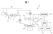
- FIG. 1 is an overall schematic configuration diagram showing an embodiment of a defect inspection device
- 4A to 4C are diagrams illustrating a first example of an illumination intensity distribution shape realized by an illumination unit.
- 4A to 4C are diagrams illustrating a first example of an illumination intensity distribution shape realized by an illumination unit.
- 13 is a diagram showing a second example of an illumination intensity distribution shape realized by the illumination unit.
- FIG. 13 is a diagram showing a third example of an illumination intensity distribution shape realized by the illumination unit.
- FIG. 13 is a diagram showing a third example of an illumination intensity distribution shape realized by the illumination unit.
- FIG. 11A and 11B are diagrams illustrating examples of optical elements included in an illumination intensity distribution control unit.
- 1A and 1B are diagrams showing the illumination distribution shape and the scanning direction on a sample surface.
- FIG. 13 is a diagram showing a trajectory of an illumination spot caused by scanning.
- FIG. 4 is a side view showing the arrangement and detection direction of the detection unit.
- FIG. 4 is a diagram showing the arrangement and detection direction of the detection unit as viewed from above.
- FIG. 4 is a diagram illustrating a first example of the configuration of a detection unit.
- FIG. 2 is a diagram showing the arrangement of illumination spots and photoelectric conversion units.
- FIG. 2 is a diagram showing the arrangement of illumination spots and photoelectric conversion units.
- FIG. 2 is a diagram showing the arrangement of illumination spots and photoelectric conversion units.
- FIG. 2 is a diagram showing the arrangement of a sample and a detection unit.
- FIG. 2 is a cross-sectional view of an image sensor.
- FIG. 13 is a graph showing the incidence angle dependence of the absorptance of an anti-reflection film.
- FIG. 13 is a graph showing the incidence angle dependence of the absorptance of an anti-reflection film.
- FIG. 11 is a diagram showing a first example of the pupil division angle dependency of the SNR of scattered light from a defect.
- FIG. 13 is a diagram showing a second example of the pupil division angle dependency of the SNR of scattered light from a defect.
- FIG. 2 illustrates a first example of a knife edge for dividing a pupil.
- FIG. 13 is a diagram showing the configuration of a detection unit in the case of oblique incidence illumination.
- FIG. 13 is a diagram showing the configuration of a detection unit in the case of vertical illumination.
- FIG. 13 shows a second example of a knife edge for dividing a pupil.
- FIG. 11 is a diagram showing a second example of the configuration of the detection unit as viewed from above.
- FIG. 11 is a side view of a second example of the configuration of the detection unit.
- FIG. 11 is a top view of a third example of the configuration of the detection unit.
- 13 is a diagram showing the configuration of a detection unit when detecting different polarized light.
- FIG. 13 is a diagram showing the configuration of a detection unit when the polarization of illumination is changed.
- FIG. 13 illustrates a third example of a knife edge for dividing a pupil.
- FIG. 2 is a diagram showing a drive mechanism of the knife edge.
- FIG. 13 is a side view of a fourth example of the configuration of the detection unit.
- the present invention will be described as being applied to a defect inspection device used in defect inspection carried out in the manufacturing process of semiconductors, etc.
- FIG. 1 is a schematic diagram of the present embodiment.
- the defect inspection device 10 has, as its main components, an illumination unit 101, a detection unit 102, photoelectric conversion units 103-1 and 103-2, a stage 104 on which a sample W can be placed and which can be moved in a direction perpendicular to the surface by an actuator, a signal processing unit 105, a control unit 53, a display unit 54, and an input unit 55.
- the illumination unit 101 appropriately comprises a laser light source 2, an attenuator 3, an emitted light adjustment unit 4, a beam expander 5, a polarization control unit 6, and an illumination intensity distribution control unit 7.
- the laser light beam emitted from the laser light source 2 is adjusted to a desired beam intensity by the attenuator 3, adjusted to a desired beam position and beam traveling direction by the emitted light adjustment unit 4, adjusted to a desired beam diameter by the beam expander 5, adjusted to a desired polarization state by the polarization control unit 6, and adjusted to a desired intensity distribution by the illumination intensity distribution control unit 7, and illuminated onto the inspection target area of the sample W.
- the angle of incidence of the illumination light on the sample surface is determined by the position and angle of the reflecting mirror of the output light adjustment unit 4 arranged in the optical path of the illumination unit 101.
- the angle of incidence of the illumination light is set to an angle suitable for detecting minute defects.
- the larger the illumination incidence angle that is, the smaller the illumination elevation angle (angle between the sample surface and the illumination optical axis), the weaker the scattered light (called haze) from minute irregularities on the sample surface, which becomes noise in the scattered light from minute foreign objects on the sample surface, and the more suitable it is for detecting minute defects.
- the incidence angle of the illumination light is preferably set to 75 degrees or more (elevation angle 15 degrees or less).
- the incidence angle of the illumination light is preferably set to 60 degrees or more and 75 degrees or less (elevation angle 15 degrees or more and 30 degrees or less).
- the polarization control in the polarization control unit 6 of the illumination unit 101 allows the illumination polarization to be P-polarized, which increases the scattered light from defects on the sample surface compared to other polarizations.
- the illumination polarization can be set to S-polarized, which reduces the scattered light from minute irregularities on the sample surface compared to other polarizations.
- the illumination optical path is changed and illumination light is irradiated from a direction substantially perpendicular to the sample surface (perpendicular illumination).
- the illumination intensity distribution on the sample surface is controlled by illumination intensity distribution control unit 7v in the same way as oblique incidence illumination.
- oblique incidence illumination and perpendicular illumination can be performed simultaneously.
- perpendicular illumination that is substantially perpendicular to the sample surface is suitable.
- the laser light source 2 To detect minute defects near the surface of the sample, the laser light source 2 must emit a short-wavelength (355 nm or less) ultraviolet or vacuum ultraviolet laser beam that does not easily penetrate the inside of the sample, and must have a high output of 2 W or more. The diameter of the emitted beam is approximately 1 mm. To detect defects inside the sample, a laser light source that emits a visible or infrared laser beam with a wavelength that easily penetrates the inside of the sample must be used.
- the attenuator 3 is appropriately equipped with a first polarizing plate, a half-wave plate that can rotate around the optical axis of the illumination light, and a second polarizing plate.
- the light incident on the attenuator 3 is converted to linearly polarized light by the first polarizing plate, and the polarization direction is rotated in an arbitrary direction according to the slow axis azimuth angle of the half-wave plate, and passes through the second polarizing plate.
- the azimuth angle of the half-wave plate By controlling the azimuth angle of the half-wave plate, the light intensity is reduced at an arbitrary ratio. If the degree of linear polarization of the light incident on the attenuator 3 is sufficiently high, the first polarizing plate is not necessarily required.
- the attenuator 3 used has a relationship between the input signal and the light reduction rate calibrated in advance.
- the output light adjustment unit 4 is equipped with multiple reflecting mirrors.
- an example is described in which it is configured with two reflecting mirrors, but this is not limited to this, and three or more reflecting mirrors may be used as appropriate.
- a three-dimensional Cartesian coordinate system (XYZ coordinates) is provisionally defined, and it is assumed that the light incident on the reflecting mirror travels in the +X direction.
- the first reflecting mirror is installed to deflect the incident light in the +Y direction (incident and reflected in the XY plane), and the second reflecting mirror is installed to deflect the light reflected by the first reflecting mirror in the +Z direction (incident and reflected in the YZ plane).
- the position and traveling direction (angle) of the light emitted from the output light adjustment unit 4 are adjusted by translating each reflecting mirror and adjusting the tilt angle.
- XY plane entrance/reflection surface
- YZ plane entrance/reflection surface
- the beam expander 5 has two or more lens groups and has the function of expanding the diameter of the parallel light beam incident thereon.
- a Galilean type beam expander having a combination of concave and convex lenses is used.
- the beam expander 5 is installed on a translation stage with two or more axes, and its position can be adjusted so that its center coincides with a specified beam position.
- the beam expander 5 is provided with a function for adjusting the tilt angle of the entire beam expander 5 so that the optical axis of the beam expander 5 coincides with a specified beam optical axis.
- the expansion rate of the light beam diameter can be controlled by adjusting the lens spacing (zoom mechanism).
- the diameter of the light beam can be expanded and collimated (the light beam is made quasi-parallel) at the same time by adjusting the lens spacing.
- the light beam can be collimated by installing a collimating lens upstream of the beam expander 5 independently of the beam expander 5.
- the beam diameter expansion factor of the beam expander 5 is about 5 to 10 times, so the beam emitted from the light source with a diameter of 1 mm is expanded to about 5 to 10 mm.
- the polarization control unit 6 is composed of a half-wave plate and a quarter-wave plate, and controls the polarization state of the illumination light to any polarization state. In the middle of the optical path of the illumination unit 101, the state of the light incident on the beam expander 5 and the light incident on the illumination intensity distribution control unit 7 is measured by the beam monitor 22.
- FIGS. 2 to 6 are schematic diagrams showing the positional relationship between the illumination optical axis 120 guided to the sample surface from the illumination unit 101 and the illumination intensity distribution shape. Note that the configuration of the illumination unit 101 in FIG. 2 to FIG. 6 shows only a part of the configuration of the illumination unit 101, and the emitted light adjustment unit 4, mirror 21, beam monitor 22, etc. are omitted.
- Figure 2 shows a schematic diagram of a cross section of the incidence plane of oblique incidence illumination (plane including the illumination optical axis and the sample surface normal).
- the oblique incidence illumination is inclined with respect to the sample surface within the incidence plane.
- the illumination unit 101 creates a substantially uniform illumination intensity distribution within the incidence plane.
- the length of the portion with uniform illumination intensity is approximately 100 ⁇ m to 4 mm in order to inspect a wide area per unit time.
- Figure 3 shows a schematic diagram of a cross section of a plane including the sample surface normal and perpendicular to the incidence plane of oblique incidence illumination. Within this plane, the illumination intensity distribution on the sample surface forms an illumination intensity distribution in which the intensity at the periphery is weaker than at the center.
- the intensity distribution is a Gaussian distribution that reflects the intensity distribution of the light incident on the illumination intensity distribution control unit 7, or an intensity distribution similar to a first-order Bessel function of the first kind or a sinc function that reflects the aperture shape of the illumination intensity distribution control unit 7.
- the length of the illumination intensity distribution in this plane (the length of the region having an illumination intensity of 13.5% or more of the maximum illumination intensity) is shorter than the length of the portion in the incident plane where the illumination intensity is uniform, and is approximately 2.5 ⁇ m to 20 ⁇ m, in order to reduce haze generated from the sample surface.
- the illumination intensity distribution control unit 7 includes optical elements such as an aspheric lens, a diffractive optical element, a cylindrical lens array, and a light pipe, which will be described later.
- the optical elements that make up the illumination intensity distribution control unit 7 are installed perpendicular to the illumination optical axis, as shown in Figures 2 and 3.
- the optical elements constituting the illumination intensity distribution control unit 7 it is possible to install the optical elements constituting the illumination intensity distribution control unit 7 at an angle to the optical axis. Also, as shown in Figures 5 and 6, it is possible to switch the intensity distribution on the incident surface of the oblique incidence illumination shown in Figures 2 and 3 with the intensity distribution on a surface perpendicular to the incident surface. In other words, it is also possible to configure the portion of uniform illumination intensity on the incident surface to be shorter than the portion of uniform illumination intensity on a surface perpendicular to the incident surface.
- the illumination intensity distribution control unit 7 is equipped with optical elements that act on the phase distribution and intensity distribution of the incident light.
- a diffractive optical element 71 (DOE: Diffractive Optical Element) is used as the optical element constituting the illumination intensity distribution control unit 7 ( Figure 7).
- the diffractive optical element 71 is formed by forming a fine undulating shape with dimensions equal to or smaller than the wavelength of light on the surface of a substrate made of a material that transmits the incident light. For ultraviolet light, fused quartz is used as a material that transmits the incident light. In order to suppress the attenuation of light due to passing through the diffractive optical element 71, it is preferable to use one that is coated with an anti-reflection film.
- Lithography is used to form the fine undulating shape of the diffractive optical element.
- an illumination intensity distribution on the sample surface that corresponds to the undulating shape of the diffractive optical element 71 is formed.
- the undulating shape of the diffractive optical element 71 is designed and manufactured to a shape calculated based on Fourier optics theory so that the illumination intensity distribution formed on the sample surface is a long and uniform distribution within the incident surface.
- the optical element provided in the illumination intensity distribution control unit 7 is provided with a translation adjustment mechanism with two or more axes and a rotation adjustment mechanism with two or more axes so that the relative position and angle with respect to the optical axis of the incident light can be adjusted.
- a focus adjustment mechanism that moves in the optical axis direction is provided.
- an aspheric lens, a combination of a cylindrical lens array and a cylindrical lens, or a combination of a light pipe and an imaging lens may be used.
- the illumination intensity distribution on the sample surface adjusted by the illumination intensity distribution control unit 7 is measured by the illumination intensity distribution monitor 24. As shown in FIG. 1, even when vertical illumination is used, the illumination intensity distribution on the sample surface adjusted by the illumination intensity distribution control unit 7v is measured by the illumination intensity distribution monitor 24.
- the illumination intensity distribution monitor 24 detects the sample surface as an image by forming an image of the sample surface on an image sensor such as a CCD sensor or CMOS sensor via a lens.
- the height displacement of the sample surface causes a displacement of the position of the illumination intensity distribution and disturbance of the illumination intensity distribution due to defocus. To prevent this, the height of the sample surface is measured, and if the height is shifted, the deviation is corrected by adjusting the height using the illumination intensity distribution control unit 7 or the Z axis of the stage 104.
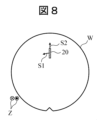
- the illuminance distribution shape (illumination spot 20) formed on the sample surface by the illumination unit 101 and the sample scanning method will be described with reference to Figures 8 and 9.
- a circular semiconductor silicon wafer is assumed as the sample W.
- the stage 104 is equipped with a translation stage, a rotation stage, and a Z stage for adjusting the height of the sample surface (none of which are shown).
- the illumination spot 20 has a long illumination intensity distribution in one direction, which direction is S2, and the direction substantially perpendicular to S2 is S1.
- the rotational motion of the rotation stage scans in the circumferential direction S1 of a circle centered on the rotation axis of the rotation stage, and the translational motion of the translation stage scans in the translation direction S2 of the translation stage.
- the illumination spot draws a spiral trajectory T on the sample W by scanning in the scanning direction S2 for a distance equal to or less than the longitudinal length of the illumination spot 20, and the entire surface of the sample W is scanned.
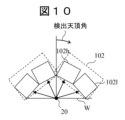
- FIG. 10 to 12 are used to explain examples of the arrangement of the detection unit 102 with respect to the sample W and the illumination spot 20.
- FIG. 10 shows a side view of the arrangement of the detection unit 102.
- the angle between the normal to the sample W and the detection direction of the detection unit is defined as the detection zenith angle.
- the detection unit 102 includes a high-angle detection unit 102h whose detection zenith angle is equal to or less than a predetermined angle and a low-angle detection unit 102l whose detection zenith angle is equal to or more than a predetermined angle.
- the configuration of the optical system of the detection unit 102 will be described later with reference to FIG. 12.
- Each of the high-angle detection unit 102h and the low-angle detection unit 102l detects scattered light using a common objective lens, and the scattered light is branched at the Fourier plane of the objective lens.
- the boundary between the detection zenith angle of the high-angle detection unit 102h and the detection zenith angle of the low-angle detection unit 102l can be easily changed.
- FIG. 1 shows one detection unit 102, but multiple detection units 102 are arranged to detect scattered light in multiple azimuths emanating from the illumination spot 20.
- FIG. 11 shows a plan view of the arrangement of the detection units 102. In a plane parallel to the surface of the sample W, the angle between the traveling direction of the oblique incidence illumination and the detection direction is defined as the detection azimuth angle.
- the detection unit 102 appropriately includes a front detection unit 102f, a rear detection unit 102b, and a front detection unit 102f' and a rear detection unit 102b' that are positioned symmetrically with respect to the illumination incidence plane.
- the front detection unit 102f is installed with a detection azimuth angle of 0 degrees or more and 90 degrees or less
- the rear detection unit 102b is installed with a detection azimuth angle of 90 degrees or more and 180 degrees or less.
- the aperture 1024 is an aperture set to pass only the light of the area detected by the photoelectric conversion unit 103 from the image of the illumination spot 20.
- the aperture 1024 passes only the central part of the Gaussian distribution where the amount of light is strong in the S2 direction, and blocks the areas at the ends of the beam where the amount of light is weak.
- the size of the image of the illumination spot 20 in the S1 direction is approximately the same as that of the image formed by the illumination spot 20, suppressing disturbances such as air scattering that occur when the illumination passes through the air.
- the condenser lens 1025 re-condenses the image of the aperture 1024 formed.
- the polarizing beam splitter 1027 separates the light whose polarization direction has been converted by the polarization control filter 1022 according to the polarization direction.
- the diffuser 1029 absorbs the light whose polarization direction is not used for detection by the photoelectric conversion unit 103. This prevents unnecessary light from becoming stray light.
- the imaging lens 1028 forms an image of the illumination spot 20 on the photoelectric conversion unit 103. As the imaging lens 1028, a cylindrical lens can also be used to form an image in only one direction.
- the polarization control filter 1022 is a 1/2 wavelength plate, and in combination with the polarizing beam splitter 1027, only light of a specific polarization direction from the light focused by the objective lens 1021 is detected by the photoelectric conversion unit 103.
- the optical system from the objective lens 1021 to the condenser lens 1025 is sometimes called the condenser optical system, and the optical system from the condenser lens 1025 to the photoelectric conversion unit 103 is sometimes called the imaging optical system.
- Figures 13 and 14 show examples of the arrangement of the photoelectric conversion unit 103.
- the optical axis 121 is inclined with respect to the normal direction of the light receiving unit 1031.
- the light receiving unit 1031 of the photoelectric conversion unit 103 is arranged parallel to the longitudinal direction of the optical image 25 formed on the light receiving unit 1031 by the detection unit 102 from the linear illumination spot 20 irradiated onto the surface of the sample W.
- the pair of cylindrical lenses 10210, 10211 form a cylindrical beam expander, which makes the spread of the optical image 25 formed by the illumination spot 20 in the short direction ⁇ smaller than the spread of this optical image 25 in the longitudinal direction.
- Figure 15 shows a schematic diagram of the three-dimensional arrangement of the sample W and the detection unit 102.
- the optical axis 121 of the detection unit 102 is inclined by an angle ⁇ (zenith angle) with respect to the normal direction Z of the sample W.
- the projection of the optical axis 121 onto the sample surface is inclined by an angle ⁇ (azimuth angle) with respect to the longitudinal direction S2 of the illumination spot 20.
- this optical axis 121 is represented by a vector v0 shown as (Equation 1).
- v0 (sin ⁇ sin ⁇ , sin ⁇ cos ⁇ cos ⁇ ) ...
- Equation 2 The angle ⁇ between the vector v0 and the longitudinal direction S2 of the illumination spot 20 is calculated by (Equation 2).
- the imaging magnification M is determined by the condenser lens 1025 and the imaging lens 1028.
- the position ⁇ Z of the image formed here is expressed by (Equation 4).
- ⁇ Z M 2 x (sin ⁇ cos ⁇ ),
- the line sensor is arranged so as to be perpendicular to the optical axis 121 which is the center of the light beam emitted by the imaging lens 1028.
- the photoelectric conversion unit 103 is tilted to realize imaging detection without defocusing, regardless of the change in the field of view of the working distance ⁇ z.
- the optical axis 121 incident on the photoelectric conversion unit 103 and the pixel array vector v1 of the light receiving surface are in a plane spanned by the longitudinal direction S2 of the illumination spot 20 and the vector v0, and the angle ⁇ between the vector v1 and the vector v0 is set to satisfy (Equation 5).
- tan ⁇ M ⁇ tan ⁇ ...(Formula 5)
- the angle ⁇ is the angle between the longitudinal vector v2 of the illumination spot 20 and the vector v0, and satisfies (Equation 6).
- the angle ⁇ between the optical axis 121 incident on the photoelectric conversion unit 103 from the imaging lens 1028 and the vector v1 can be maximized.
- the numerical aperture of the incident light beam on the focusing lens 1025 is N
- the spread of the light beam emitted to the photoelectric conversion unit 103 is the reciprocal of the imaging magnification M multiplied by the spread of the light beam emitted to the imaging lens 1028.
- the imaging magnification M is set to 1x or more. As a result, the angle ⁇ becomes smaller than the angle ⁇ , and typically becomes smaller by 5 degrees or more when a magnification of about 1.3x is applied.
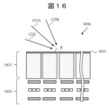
- FIG. 16 shows a cross-sectional view of the image sensor 1036 that constitutes the photoelectric conversion unit 103.
- the image sensor 1036 is constructed by laminating an anti-reflection film 1033, a light receiving unit 1031, and a wiring unit 1032 in this order from the surface.
- Incident light 122A to 122C is light that enters the image sensor 1036.
- Incoming light 122A is light on optical axis 121 shown in Figures 13 and 14.
- Incident light 122B, 122C is light incident from an angle different from optical axis 121.
- Anti-reflection film 1033 is a film for preventing surface reflection of incident light 122A to 122C.
- Light receiving section 1031 is in an array shape, and performs photoelectric conversion for each divided area, i.e., pixel.
- Wiring section 1032 independently extracts the electricity output by light receiving section 1031 to the outside.
- a sensor having such a structure in which light receiving section 1031 is located closer to the light incident side than wiring section 1032 is known as a back side illumination sensor.
- incident light 122 is incident at a predetermined angle shifted from the normal direction of light receiving section 1031.
- FSI Front Side Illumination
- incident light 122A to 122C As shown by incident light 122A to 122C, light is incident on the light receiving section 1031 from various directions. Therefore, unless the anti-reflection film 1033 has a high absorption rate for these incident light beams 122A to 122C, good sensitivity cannot be obtained.
- FIG. 17 is a graph showing the characteristics of the anti-reflection film 1033 formed of a single layer of HfO 2 25 nm.
- the horizontal axis of the graph shows the angle of incidence, and the vertical axis of the graph shows the absorptance.
- Curve 10333 shows the characteristics of the absorptance of S-polarized light
- curve 10334 shows the characteristics of the absorptance of P-polarized light.
- the absorptance of P-polarized light decreases as the angle of incidence increases, but the absorptance drops to 0.5 when the angle of incidence is around 60 degrees.
- the angle of incidence of S-polarized light increases up to about 70 degrees, and in the range of angles of incidence from 0 to 80 degrees, the absorptance is 70% or more.
- the photoelectric conversion units 103-1 and 103-2 need to be inclined by a predetermined angle in order to realize imaging detection without focus shifting, regardless of changes in the field of view of the working distance. In other words, it is desirable to incline the normal of the light receiving surface of the photoelectric conversion unit 103-1 by, for example, 10 to 80 degrees from the optical axis 121 of the detection unit 102.
- ⁇ Pupil division adjustment using a knife edge with a linear motion mechanism A method of adjusting the pupil division of the detection unit according to the inspection object or inspection conditions will be described.
- the intensity distribution of scattered light from defects and background scattered light differs depending on the state of the surface of the sample to be inspected. For example, in the case of a film-coated wafer that has undergone an oxidation process to form a protective film covering the semiconductor wafer surface in the semiconductor manufacturing process, the SN ratio (ratio of defect scattered light to background scattered light) on the low-angle detector side with a large detection zenith angle is larger than that of a bare wafer without a film.
- the sensitivity can be improved by widening the aperture of the low-angle detector. Therefore, the knife edge 1026 is moved by the linear motion mechanism 10213 (see FIG. 12) according to the inspection object, and the distribution of the aperture is changed by adjusting the division angle.
- the linear motion mechanism 10213 and the knife edge 1026 are sometimes collectively referred to as a pupil division mechanism.
- Figures 18 and 19 are graphs showing the characteristics of defect measurement sensitivity versus the division angle of the zenith angle by the knife edge 1026.
- Figure 18 is a graph for a bare wafer
- Figure 19 is a graph for a wafer with a film.
- the highest sensitivity can be obtained by setting the division angle to 40 degrees (see Figure 18) when the wafer to be inspected is a bare wafer, and by setting the division angle to 60 degrees (see Figure 19) when the wafer to be inspected is a wafer with an oxide film.
- the pupil division angle is set for each of the multiple detection units.
- the sensitivity can be improved by setting different division angles for the front detection unit 102f and the rear detection unit 102b.
Landscapes
- Physics & Mathematics (AREA)
- General Physics & Mathematics (AREA)
- Optics & Photonics (AREA)
- Health & Medical Sciences (AREA)
- Life Sciences & Earth Sciences (AREA)
- Chemical & Material Sciences (AREA)
- Analytical Chemistry (AREA)
- Biochemistry (AREA)
- General Health & Medical Sciences (AREA)
- Immunology (AREA)
- Pathology (AREA)
- Investigating Materials By The Use Of Optical Means Adapted For Particular Applications (AREA)
Abstract
Description
本発明は欠陥検査装置及びその検出部の光学系に関する。例えば試料表面に存在する微小な欠陥を検査し、欠陥の位置、種類および寸法を判定して出力する欠陥検査装置及びその検出部の光学系に関する。 The present invention relates to a defect inspection device and the optical system of its detection section. For example, the present invention relates to a defect inspection device and the optical system of its detection section that inspects minute defects present on a sample surface, and determines and outputs the position, type, and size of the defect.
半導体基板や薄膜基板等の製造ラインにおいて、製品の歩留りを維持・向上するために、半導体基板や薄膜基板等の表面に存在する欠陥の検査が行われている。欠陥検査の従来技術としては例えば特表2014-504370号公報(特許文献1)が知られている。 In manufacturing lines for semiconductor substrates, thin film substrates, etc., inspections are conducted for defects present on the surfaces of semiconductor substrates, thin film substrates, etc., in order to maintain and improve product yields. For example, JP2014-504370A (Patent Document 1) is known as a conventional defect inspection technique.
特許文献1では、「集光サブシステムの集光開口数(NA)の異なるセグメントへの分割と、異なるセグメント中に集光された散乱光の別個の検出器への方向付けとを行うように構成される」構成について述べられており、その実施例として集光サブシステムのフーリエ面に配置したアパチャ鏡について「アパチャ鏡は、集光NAの1つのセグメント中に集光された散乱光を透過させつつ、集光NAの別のセグメント中に集光された散乱光を反射する」と記載されている。また、「異なるセグメントのうち1つの中の散乱光を偏光に基づいて分離して、散乱光の異なる部分とするように構成」し、ウェハ表面からの表面散乱を抑制する技術が開示されている。
特許文献2では、微小な欠陥から発生する散乱光を検出するために、試料面に対して傾斜した方向に検出系を複数配置し、それぞれの検出系で試料面に照射した線状照明の像をセンサ位置に結像して欠陥判定を行っている。線状照明の像を斜方から検出できるように光学系を配置すると、検出部と試料面の線状照明部との間の作動距離が視野内で変化する。このとき、焦点ずれが生じるため、センサ面で結像される像の解像度が低下する。これを抑制するために、特許文献1には、被検査対象基板Wに対する検出方向の傾きに応じて、被検査対象基板Wと共役になるようにセンサを傾斜させることで、被検査対象基板W上の像を検出器上に斜方から結像できることが記載されている。
In
半導体等の製造工程で用いられる欠陥検査には、微小な欠陥を検出すること、検出した欠陥の寸法を高精度に計測すること、試料を非破壊で(例えば試料を変質させることなく)検査すること、同一の試料を検査した場合に例えば検出欠陥の個数、位置、寸法、欠陥種に関して実質的に一定の検査結果が得られること、一定時間内に多数の試料を検査すること、などが求められる。 The defect inspection used in the manufacturing process of semiconductors and other products requires the detection of minute defects, the measurement of the dimensions of detected defects with high precision, the inspection of the sample non-destructively (i.e. without altering the sample), the obtaining of substantially consistent inspection results in terms of, for example, the number, position, dimensions, and type of defects when inspecting the same sample, and the inspection of a large number of samples within a certain period of time.
特許文献1に述べられた技術では、20nm以下の微小な欠陥についても検査を実現できるよう、背景散乱光との弁別を対物レンズのフーリエ面に備えた「アパチャ鏡」を用いて光路を分岐させ、分岐した光路毎にさらに偏光に応じて光路を分岐させている。
In the technology described in
光路を分岐させる検査方法では、検査対象となる試料表面の状態により欠陥からの散乱光と背景散乱光が伝搬する方向が異なるため、最高感度を与える光路分岐の条件が異なる。また、照明の入射方向などの検査条件によっても最高感度を与える光路分岐条件は異なる。 In inspection methods that branch the optical path, the directions in which scattered light from defects and background scattered light propagate differ depending on the condition of the sample surface being inspected, so the optical path branching conditions that give the highest sensitivity differ. In addition, the optical path branching conditions that give the highest sensitivity also differ depending on inspection conditions such as the incident direction of the illumination.
本発明の目的は、検査対象あるいは検査条件に応じて最適な光路分岐条件を達成することが可能な欠陥検査装置を提供することにある。 The object of the present invention is to provide a defect inspection device that can achieve optimal optical path branching conditions depending on the inspection object or inspection conditions.
上記課題を解決するために、例えば特許請求の範囲に記載の構成を採用する。その一例を挙げるならば、光源から射出された照明光を試料に照射する照明部と、試料に対して斜方方向に配置され、試料から発生する散乱光を検出する検出部と、検出部の瞳を第1の検出角度と第2の検出角度とに分割する瞳分割機構と、検出部によって検出された第1の検出角度の散乱光を電気信号に変換する第1の光電変換部と、検出部によって検出された第2の検出角度の散乱光を電気信号に変換する第2の光電変換部と、第1の光電変換部及び第2の光電変換部により変換された電気信号を処理して試料の欠陥を検出する信号処理部とを有する欠陥検査装置であって、瞳分割機構は、検査対象または検査条件に応じた瞳の配分となるよう瞳を分割する。 In order to solve the above problem, for example, the configuration described in the claims is adopted. One example is a defect inspection device having an illumination unit that irradiates the sample with illumination light emitted from a light source, a detection unit that is arranged in an oblique direction with respect to the sample and detects scattered light generated from the sample, a pupil splitting mechanism that splits the pupil of the detection unit into a first detection angle and a second detection angle, a first photoelectric conversion unit that converts the scattered light at the first detection angle detected by the detection unit into an electrical signal, a second photoelectric conversion unit that converts the scattered light at the second detection angle detected by the detection unit into an electrical signal, and a signal processing unit that processes the electrical signals converted by the first photoelectric conversion unit and the second photoelectric conversion unit to detect defects in the sample, and the pupil splitting mechanism splits the pupil so as to achieve a pupil distribution according to the inspection target or inspection conditions.
本発明によれば、検出部の瞳を検査対象または検査条件に応じた配分となるよう分割することで、背景散乱光を弁別して、微小な欠陥から散乱する光を高感度に検出する。前述した以外の課題、構成及び効果は、以下の実施の形態の説明により明らかにされる。 According to the present invention, the pupil of the detection unit is divided so that its distribution corresponds to the inspection object or inspection conditions, thereby discriminating background scattered light and detecting light scattered from minute defects with high sensitivity. Problems, configurations, and effects other than those described above will become clear from the explanation of the embodiment below.
以下、本発明の実施の形態を、図を用いて説明する。なお、本発明は以下に説明する実施例に限定されるものではなく、様々な変形例が含まれる。以下で説明する実施例は、本発明を分かり易く説明するために詳細に説明するものであり、必ずしも説明した全ての構成を備えるものに限定されるものではない。また、ある実施例の構成の一部を他の実施例に置き換えることが可能であり、また、ある実施例の構成に他の実施例を加えることも可能である。また各実施例の構成の一部について、他の構成の追加、削除、置換をすることが可能である。 Below, an embodiment of the present invention will be described with reference to the drawings. Note that the present invention is not limited to the examples described below, and various modified examples are included. The examples described below are described in detail to explain the present invention in an easy-to-understand manner, and are not necessarily limited to those having all of the configurations described. It is also possible to replace part of the configuration of one example with another example, and it is also possible to add other examples to the configuration of one example. It is also possible to add, delete, or replace part of the configuration of each example with other configurations.
以下の実施例では、本発明を、半導体等の製造工程で実行する欠陥検査に用いられる欠陥検査装置に適用する場合について説明する。 In the following embodiment, the present invention will be described as being applied to a defect inspection device used in defect inspection carried out in the manufacturing process of semiconductors, etc.
図1は本実施例の概略構成図である。欠陥検査装置10は、その主要部として、照明部101、検出部102、光電変換部103-1,103-2、試料Wを載置可能でアクチュエータで面直方向に移動可能なステージ104、信号処理部105、制御部53、表示部54、入力部55を有する。
FIG. 1 is a schematic diagram of the present embodiment. The
照明部101は、レーザ光源2、アッテネータ3、出射光調整部4、ビームエキスパンダ5、偏光制御部6、照明強度分布制御部7を適宜備える。レーザ光源2から射出されたレーザ光ビームは、アッテネータ3で所望のビーム強度に調整され、出射光調整部4で所望のビーム位置、ビーム進行方向に調整され、ビームエキスパンダ5で所望のビーム径に調整され、偏光制御部6で所望の偏光状態に調整され、照明強度分布制御部7で所望の強度分布に調整され、試料Wの検査対象領域に照明される。
The
照明部101の光路中に配置された出射光調整部4の反射ミラーの位置と角度により、試料表面に対する照明光の入射角が決められる。照明光の入射角は微小な欠陥の検出に適した角度に設定される。照明入射角が大きいほど、すなわち照明仰角(試料表面と照明光軸との成す角)が小さいほど、試料表面上の微小異物からの散乱光に対してノイズとなる試料表面の微小凹凸からの散乱光(ヘイズと呼ばれる)が弱まるため、微小な欠陥の検出に適する。このため、試料表面の微小凹凸からの散乱光が微小欠陥検出の妨げとなる場合には、照明光の入射角は好ましくは75度以上(仰角15度以下)に設定するのがよい。一方、斜入射照明において照明入射角が小さいほど微小異物からの散乱光の絶対量が大きくなるため、欠陥からの散乱光量の不足が微小欠陥検出の妨げとなる場合には、照明光の入射角は好ましくは60度以上75度以下(仰角15度以上30度以下)に設定するのがよい。また、斜入射照明を行う場合、照明部101の偏光制御部6における偏光制御により、照明の偏光をP偏光とすることで、その他の偏光と比べて試料表面上の欠陥からの散乱光が増加する。また、試料表面の微小凹凸からの散乱光が微小欠陥検出の妨げとなる場合には、照明の偏光をS偏光とすることで、その他の偏光と比べて試料表面の微小凹凸からの散乱光が減少する。
The angle of incidence of the illumination light on the sample surface is determined by the position and angle of the reflecting mirror of the output
必要に応じて、図1に示すように、照明部101の光路中にミラー21を挿入し、適宜他のミラーを配置することにより、照明光路が変更され、試料面に対して実質的に垂直な方向から照明光が照射される(垂直照明)。このとき、試料面上の照明強度分布は照明強度分布制御部7vにより、斜入射照明と同様に制御される。ミラー21と同じ位置にビームスプリッタを挿入することで、斜入射照明と垂直照明とを同時に行うことができる。試料面の凹み状の欠陥(研磨キズや結晶材料における結晶欠陥)からの散乱光を得るには、試料表面に実質的に垂直に入射する垂直照明が適する。
If necessary, as shown in FIG. 1, by inserting
試料表面近傍の微小な欠陥を検出するには、レーザ光源2として、試料内部に浸透しづらい波長である短波長(波長355nm以下)の紫外または真空紫外のレーザビームを発振するものであり、かつ出力2W以上の高出力のものを用いる。出射ビーム径は1mm程度である。試料内部の欠陥を検出するには、試料内部に浸透しやすい波長として、可視あるいは赤外のレーザビームを発振するものを用いる。
To detect minute defects near the surface of the sample, the
アッテネータ3は、第1の偏光板と、照明光の光軸周りに回転可能な1/2波長板と、第2の偏光板を適宜備える。アッテネータ3に入射した光は、第1の偏光板により直線偏光に変換され、1/2波長板の遅相軸方位角に応じて偏光方向が任意の方向に回転され、第2の偏光板を通過する。1/2波長板の方位角を制御することで、光強度が任意の比率で減光される。アッテネータ3に入射する光の直線偏光度が十分高い場合は第1の偏光板は必ずしも必要ない。アッテネータ3は入力信号と減光率との関係が事前に較正されたものを用いる。アッテネータ3として、グラデーション濃度分布を持つNDフィルタを用いることも、互いに異なる複数の濃度のNDフィルタを切替えて使用することも可能である。
The
出射光調整部4は複数枚の反射ミラーを備える。ここでは2枚の反射ミラーで構成した場合の実施例を説明するが、これに限られるものではなく、3枚以上の反射ミラーを適宜用いても構わない。ここで、三次元の直交座標系(XYZ座標)を仮に定義し、反射ミラーへの入射光が+X方向に進行しているものと仮定する。第1の反射ミラーは入射光を+Y方向に偏向するよう設置され(XY面内での入射・反射)、第2の反射ミラーは第1の反射ミラーで反射した光を+Z方向に偏向するよう設置される(YZ面内での入射・反射)。各々の反射ミラーは平行移動とあおり角調整により、出射光調整部4から出射する光の位置、進行方向(角度)が調整される。前記のように、第1の反射ミラーの入射・反射面(XY面)と第2の反射ミラー入射・反射面(YZ面)が直交するような配置とすることで、出射光調整部4から出射する光(+Z方向に進行)のXZ面内の位置、角度調整と、YZ面内の位置、角度調整とを独立に行うことができる。
The output
ビームエキスパンダ5は二群以上のレンズ群を有し、入射する平行光束の直径を拡大する機能を持つ。例えば、凹レンズと凸レンズの組合せを備えるガリレオ型のビームエキスパンダが用いられる。ビームエキスパンダ5は二軸以上の並進ステージに設置され、所定のビーム位置と中心が一致するように位置調整が可能である。また、ビームエキスパンダ5の光軸と所定のビーム光軸が一致するようにビームエキスパンダ5全体のあおり角調整機能が備えられる。レンズの間隔を調整することにより、光束直径の拡大率を制御することが可能である(ズーム機構)。ビームエキスパンダ5に入射する光が平行でない場合には、レンズの間隔の調整により、光束の直径の拡大とコリメート(光束の準平行光化)が同時に行われる。光束のコリメートはビームエキスパンダ5の上流にビームエキスパンダ5と独立にコリメートレンズを設置して行ってもよい。ビームエキスパンダ5によるビーム径の拡大倍率は5倍から10倍程度であり、光源から出射したビーム径1mmのビームが5mmから10mm程度に拡大される。
The
偏光制御部6は、1/2波長板、1/4波長板によって構成され、照明光の偏光状態を任意の偏光状態に制御する。照明部101の光路の途中において、ビームモニタ22によって、ビームエキスパンダ5に入射する光、および照明強度分布制御部7に入射する光の状態が計測される。
The
図2乃至図6に、照明部101より試料面に導かれる照明光軸120と照明強度分布形状との位置関係の模式図を示す。なお、図2乃至図6における照明部101の構成は照明部101の構成の一部を示したものであり、出射光調整部4、ミラー21、ビームモニタ22等は省略されている。
FIGS. 2 to 6 are schematic diagrams showing the positional relationship between the illumination
図2に、斜入射照明の入射面(照明光軸と試料表面法線とを含む面)の断面の模式図を示す。斜入射照明は入射面内にて試料表面に対して傾斜している。照明部101により入射面内において実質的に均一の照明強度分布が作られる。照明強度が均一である部分の長さは、単位時間当たりに広い面積を検査するため、100μmから4mm程度である。図3に、試料表面法線を含みかつ斜入射照明の入射面に垂直な面の断面の模式図を示す。この面内で、試料面上の照明強度分布は中心に対して周辺の強度が弱い照明強度分布を成す。より具体的には、照明強度分布制御部7に入射する光の強度分布を反映したガウス分布、あるいは照明強度分布制御部7の開口形状を反映した第一種第一次のベッセル関数あるいはsinc関数に類似した強度分布となる。この面内での照明強度分布の長さ(最大照明強度の13.5%以上の照明強度を持つ領域の長さ)は、試料表面から発生するヘイズを低減するため、前記入射面内における照明強度が均一である部分の長さより短く、2.5μmから20μm程度である。照明強度分布制御部7は、後述する非球面レンズ、回折光学素子、シリンドリカルレンズアレイ、ライトパイプなどの光学素子を備える。照明強度分布制御部7を構成する光学素子は図2、図3に示されるように、照明光軸に垂直に設置される。
Figure 2 shows a schematic diagram of a cross section of the incidence plane of oblique incidence illumination (plane including the illumination optical axis and the sample surface normal). The oblique incidence illumination is inclined with respect to the sample surface within the incidence plane. The
また、図4に示されるように、照明強度分布制御部7を構成する光学素子を光軸に傾けて設置することも可能である。また、図5及び図6に示すように、図2及び図3で示した斜入射照明の入射面での強度分布と入射面に垂直な面での強度分布を入れ替えることも可能である。すなわち、入射面における照明強度の均一な部分が、入射面に垂直な面における照明強度の均一な部分に比べて短くなっている構成も可能である。
Also, as shown in Figure 4, it is possible to install the optical elements constituting the illumination intensity
照明強度分布制御部7は入射する光の位相分布および強度分布に作用する光学素子を備える。照明強度分布制御部7を構成する光学素子として、回折光学素子71(DOE:Diffractive Optical Element)が用いられる(図7)。回折光学素子71は、入射光を透過する材質からなる基板の表面に、光の波長と同等以下の寸法の微細な起伏形状を形成したものである。入射光を透過する材質として、紫外光用には溶融石英が用いられる。回折光学素子71を通過することによる光の減衰を抑えるため、反射防止膜によるコーティングが施されたものを用いるとよい。回折光学素子の微細な起伏形状の形成にはリソグラフィ法が用いられる。ビームエキスパンダ5を通過後に準平行光となった光を、回折光学素子71を通過させることにより、回折光学素子71の起伏形状に応じた試料面上照明強度分布が形成される。回折光学素子71の起伏形状は、試料表面上で形成される照明強度分布が入射面内に長く均一な分布となるよう、フーリエ光学理論を用いた計算に基づいて求められた形状に設計され、製作される。照明強度分布制御部7に備えられる光学素子は、入射光の光軸との相対位置、角度が調整可能となるよう、二軸以上の並進調整機構、および二軸以上の回転調整機構が備えられる。さらに、光軸方向の移動によるフォーカス調整機構が設けられる。回折光学素子71と同様の機能を持つ代替の光学素子として、非球面レンズ、シリンドリカルレンズアレイとシリンドリカルレンズとの組合せ、ライトパイプと結像レンズとの組合せを用いてもよい。
The illumination intensity
照明部101によって試料面上に作られる照明強度分布の変形例を説明する。一方向に長く(線状の)、長手方向に関して実質的に均一な強度を持つ照明強度分布の代替として、長手方向に関してガウス分布を持つ照明強度分布を用いることも可能である。一方向に長いガウス分布照明は、照明強度分布制御部7に球面レンズを有し、ビームエキスパンダ5にて一方向に長い楕円ビームを形成する構成とすること、あるいは照明強度分布制御部7をシリンドリカルレンズを含む複数のレンズで構成すること、などにより形成される。照明強度分布制御部7が有する球面レンズあるいはシリンドリカルレンズの一部あるいは全部は、試料面に対して平行に設置されることで、試料面上の一方向に長く、それに垂直な方向の幅の狭い照明強度分布が形成される。均一な照明強度分布を作る場合に比べて、照明強度分布制御部7に入射する光の状態の変動による試料面上の照明強度分布の変動が小さく、照明強度分布の安定性が高い、また照明強度分布制御部7に回折光学素子やマイクロレンズアレイなどを用いる場合と比べて光の透過率が高く効率がよい、という特長がある。
A modified example of the illumination intensity distribution created on the sample surface by the
照明部101における照明光の状態はビームモニタ22によって計測される。ビームモニタ22は、出射光調整部4を通過した照明光の位置および角度(進行方向)、あるいは照明強度分布制御部7に入射する照明光の位置および波面を計測して出力する。照明光の位置計測は、照明光の光強度の重心位置を計測することによって行われる。具体的な位置計測手段としては、光位置センサ(PSD:Position Sensitive Detector)、あるいはCCDセンサやCMOSセンサなどのイメージセンサが用いられる。照明光の角度計測は位置計測手段より光源から遠く離れた位置、あるいはコリメートレンズによる集光位置に設置された光位置センサあるいはイメージセンサによって行われる。センサにより検出された照明光位置、照明光角度は制御部53に入力され、表示部54に表示される。照明光位置あるいは角度が所定の位置あるいは角度からずれていた場合は、出射光調整部4によって所定の位置に戻るよう調整される。
The state of the illumination light in the
照明光の波面計測は、照明強度分布制御部7に入射する光の平行度を測定するために行われる。波面計測により照明強度分布制御部7に入射する光が準平行光でなく、発散あるいは収束していることが判明した場合、前段のビームエキスパンダ5のレンズ群を光軸方向に変位させることで、準平行光に近づけることができる。また、波面計測により照明強度分布制御部7に入射する光の波面が部分的に傾斜していることが判明した場合、空間光変調素子(SLM:Spatial Light Modulator)の一種である空間光位相変調素子を照明強度分布制御部7の前段に挿入し、波面が平坦になるよう光束断面の位置ごとに適当な位相差を与えることで、波面を平坦に近づける、すなわち照明光を準平行光に近づけることができる。以上の波面精度計測・調整手段により、照明強度分布制御部7に入射する光の波面精度(所定の波面(設計値あるいは初期状態)からのずれ)がλ/10rms以下に抑えられる。
The wavefront measurement of the illumination light is performed to measure the parallelism of the light incident on the illumination intensity
照明強度分布制御部7において調整された試料面上の照明強度分布は、照明強度分布モニタ24によって計測される。なお、図1で示したように、垂直照明を用いる場合でも、同様に、照明強度分布制御部7vにおいて調整された試料面上の照明強度分布が照明強度分布モニタ24によって計測される。照明強度分布モニタ24はレンズを介して試料面をCCDセンサやCMOSセンサなどのイメージセンサ上に結像して画像として検出するものである。照明強度分布モニタ24で検出された照明強度分布の画像は制御部53において処理され、強度の重心位置、最大強度、最大強度位置、照明強度分布の幅、長さ(所定の強度以上あるいは最大強度値に対して所定の比率以上となる照明強度分布領域の幅、長さ)などが算出され、表示部54において照明強度分布の輪郭形状、断面波形などと共に表示される。
The illumination intensity distribution on the sample surface adjusted by the illumination intensity
斜入射照明を行う場合、試料面の高さ変位によって、照明強度分布の位置の変位およびデフォーカスによる照明強度分布の乱れが起こる。これを抑制するため、試料面の高さを計測し、高さがずれた場合は照明強度分布制御部7、あるいはステージ104のZ軸による高さ調整によりずれを補正する。
When performing oblique incidence illumination, the height displacement of the sample surface causes a displacement of the position of the illumination intensity distribution and disturbance of the illumination intensity distribution due to defocus. To prevent this, the height of the sample surface is measured, and if the height is shifted, the deviation is corrected by adjusting the height using the illumination intensity
照明部101によって試料面上に形成される照度分布形状(照明スポット20)と試料走査方法について図8及び図9を用いて説明する。試料Wとして円形の半導体シリコンウェハを想定する。ステージ104は、並進ステージ、回転ステージ、試料面高さ調整のためのZステージ(いずれも図示せず)を備える。照明スポット20は前述の通り一方向に長い照明強度分布を持ち、その方向をS2とし、S2に実質的に直交する方向をS1とする。回転ステージの回転運動によって、回転ステージの回転軸を中心とした円の円周方向S1に、並進ステージの並進運動によって、並進ステージの並進方向S2に走査される。走査方向S1の走査により試料を1回転する間に、走査方向S2へ照明スポット20の長手方向の長さ以下の距離だけ走査することにより、照明スポットが試料W上にてらせん状の軌跡Tを描き、試料Wの全面が走査される。
The illuminance distribution shape (illumination spot 20) formed on the sample surface by the
以下、瞳分割した検出部について説明する。 The pupil-split detection section is explained below.
検出部102の試料Wおよび照明スポット20に対する配置例について図10乃至図12を用いて説明する。図10に検出部102の配置の側面図を示す。試料Wの法線に対して、検出部による検出方向のなす角を検出天頂角と定義する。検出部102は、検出天頂角が所定の角度以下の高角検出部102hと検出天頂角が所定の角度以上の低角検出部102lを含んで構成される。検出部102の光学系の構成は図12を用いて後述するが、高角検出部102h、低角検出部102lの各々は、共通の対物レンズを用いて散乱光を検出し、対物レンズのフーリエ面において分岐される。本実施例では、高角検出部102hの検出天頂角と低角検出部102lの検出天頂角との境界を容易に変更することができる。
10 to 12 are used to explain examples of the arrangement of the
図1には1つの検出部102を示しているが、検出部102は、照明スポット20から発する複数の方位の散乱光を検出するよう、複数配置される。図11に、検出部102の配置の平面図を示す。試料Wの表面と平行な平面内において、斜入射照明の進行方向と検出方向とのなす角を検出方位角と定義する。検出部102は、前方検出部102f、後方検出部102b、およびそれらと照明入射面に関して対称な位置にある前方検出部102f’、後方検出部102b’を適宜備える。例えば、前方検出部102fは検出方位角が0度以上90度以下、後方検出部102bは検出方位角が90度以上180度以下に設置される。これに限られず、検出部の数・位置を適宜変更してもよい。
1 shows one
検出部102の具体的な構成図の例を図12に示す。照明スポット20から発生する散乱光を対物レンズ1021によって集光し、偏光制御フィルタ1022によって偏光方向を制御する。偏光制御フィルタ1022としては、たとえばモータ等の駆動機構により回転角度を制御可能にした1/2波長板を適用する。散乱光を効率良く検出するため、対物レンズ1021の検出NAは0.3以上にするのが好ましい。対物レンズ1021の下端が試料面Wに干渉しないよう、必要に応じて対物レンズの下端を切り欠く。結像レンズ1023は照明スポット20の像をアパーチャ1024の位置に結像する。アパーチャ1024は照明スポット20の結像した像のうち、光電変換部103で検出する領域の光のみを通すように設定したアパーチャである。照明スポット20がS2方向にガウス分布のプロファイルを有する場合には、アパーチャ1024はガウス分布のうち、S2方向に光量の強い中心部のみを通過させ、ビーム端の光量の弱い領域は遮光する。また、S1方向には照明スポット20の結像した像と同程度のサイズとして、照明が空気を透過する際に発生する空気散乱等の外乱を抑制する。集光レンズ1025は、結像されたアパーチャ1024の像を再度集光する。
Figure 12 shows an example of a specific configuration diagram of the
ナイフエッジ(分岐光学部材)1026は、その先端が対物レンズ1021のフーリエ面(瞳面)Pに位置するよう配置されている。ナイフエッジ1026により、例えば、検出天頂角が45度以下の高角検出部102hと検出天頂角が45度以上の低角検出部102lに分岐する。ナイフエッジ1026は直動機構10213を備えており、瞳面Pに対して、分割された領域の境界を移動させることができる。直動機構の例としてはリニアステージがある。これにより天頂角の分割角度は必ずしも45度ではなく、適宜変えることができる。
The knife edge (branching optical element) 1026 is positioned so that its tip is located at the Fourier plane (pupil plane) P of the
偏光ビームスプリッタ1027は、偏光制御フィルタ1022で偏光方向を変換した光を偏光方向により分離する。ディフューザ1029により、光電変換部103の検出に用いない偏光方向の光を吸収する。これにより、不要な光が迷光になることを防ぐことができる。結像レンズ1028は照明スポット20の像を光電変換部103上に形成する。結像レンズ1028として、シリンドリカルレンズを用いて1方向のみの結像を行うこともできる。なお、この実施例では偏光制御フィルタ1022を1/2波長板として、偏光ビームスプリッタ1027とのコンビネーションにより、対物レンズ1021で集光した光のうち特定の偏光方向の光のみを光電変換部103で検出するようにしているのに対して、たとえば偏光制御フィルタ1022を透過率80%以上のワイヤグリッド偏光板とし、偏光ビームスプリッタ1027を用いないで所望の偏光方向の光のみを取り出すことも可能である。
The
なお、図12に示す検出部の光学系において、対物レンズ1021から集光レンズ1025までの光学系を集光光学系、集光レンズ1025から光電変換部103までの光学系を結像光学系と呼ぶこともある。
In the optical system of the detection unit shown in FIG. 12, the optical system from the
図13と図14は光電変換部103の配置の例を示している。光軸121は受光部1031の法線方向に対して傾斜している。光電変換部103の受光部1031は、試料Wの表面に照射された線状の照明スポット20が、検出部102によって受光部1031上に結像する光学像25の長手方向と平行に配置される。対となるシリンドリカルレンズ10210,10211は、シリンドリカルビームエキスパンダを構成し、照明スポット20が結像した光学像25の短手方向γの広がりを、この光学像25の長手方向の広がりよりも小さくしている。
Figures 13 and 14 show examples of the arrangement of the
光電変換部103は、光学像25を撮像して電気信号として出力する。光電変換部103は、試料Wの表面に照射された照明スポット20と共役の位置にアレイ状の受光部1031と反射防止膜(図示せず)とを備えている。光電変換部103の受光面は、短手方向γにおいて試料面と共役ではない。しかし、短手方向γは照明スポット20の短手方向でもあるため、光学像25の像高は低く、焦点ずれはほとんど発生しない。よって、短手方向γにおける光学像25の結像倍率を大きくすることで、受光部1031への入射角度のばらつきを小さくすることができる。
The
図15に、試料Wと検出部102との立体的な配置の概略図を示す。検出部102の光軸121は、試料Wの法線方向Zに対して角度θ(天頂角)だけ傾斜している。光軸121の試料面への射影は、照明スポット20の長手方向S2に対して角度φ(方位角)だけ傾斜している。
Figure 15 shows a schematic diagram of the three-dimensional arrangement of the sample W and the
このように、検出部102の光を検出する光軸121が、試料Wの法線方向Zに対して角度θ、照明スポット20の長手方向S2に対して角度φだけずれていたとすると、3次元空間において、この光軸121は、(式1)として示されるベクトルv0で表される。
v0=(sinθ・sinφ,sinθ・cosφ・cosθ) …(式1)
ベクトルv0と照明スポット20の長手方向S2とがなす角度αは、(式2)により求められる。
α=arccos(sinθ・cosφ) …(式2)
このとき、欠陥検査装置10は、光電変換部103により照明スポット20の長手方向S2に2Lの区間を検出する。視野中心からの位置xにより、作動距離(試料Wと検出部102の距離)Δzは(式3)のように示される。
Δz=x(sinθ・cosφ),|x|<L …(式3)
なお、(式3)中、|x|<Lは視野中心からの距離がL以下である、すなわち照明スポット20内の位置であることを示している。(式4)についても同じである。
In this way, if the
v0=(sinθ・sinφ, sinθ・cosφ・cosθ) … (Formula 1)
The angle α between the vector v0 and the longitudinal direction S2 of the
α=arccos(sinθ・cosφ)…(Formula 2)
At this time, the
Δz=x(sinθ・cosφ), |x|<L...(Formula 3)
In addition, in (Equation 3), |x|<L indicates that the distance from the center of the field of view is equal to or less than L, that is, the position is within the
結像倍率Mは、集光レンズ1025と結像レンズ1028によって決定される。ここで結像される像の位置ΔZは、(式4)のように表される。
ΔZ=M2x(sinθ・cosφ),|x|<L …(式4)
一般にラインセンサは、結像レンズ1028が放射する光束の中心である光軸121に対して、直交するように配置される。しかし、本実施形態では、光電変換部103を傾斜させることにより、作動距離Δzの視野内の変化によらず、焦点ずれのない結像検出を実現する。このとき、光電変換部103に入射する光軸121と受光面の画素並びベクトルv1は、照明スポット20の長手方向S2とベクトルv0によって張られる平面内にあり、かつベクトルv1とベクトルv0とのなす角βは(式5)を満たすように設定する。
tanα=M・tanβ …(式5)
ここで、角度αは照明スポット20の長手方向ベクトルv2とベクトルv0のなす角度であり、(式6)を満たす。
cosα=sinθ・cosφ …(式6)
(式5)より、結像倍率Mが大きくなると、ベクトルv0とベクトルv1のなす角度βが小さくなって入射角が大きくなる。M=2のとき、最も入射角の大きい光線は90度に近い角度で光電変換部103に入射することになる。光電変換部103の反射防止膜の吸収率は入射角度依存性をもち、90度に近い入射角では吸収率が非常に小さくなる。これを防ぐため、結像倍率Mは2倍以下に設定することが望ましい。
The imaging magnification M is determined by the
ΔZ=M 2 x (sinθ・cosφ), |x|<L...(Formula 4)
Generally, the line sensor is arranged so as to be perpendicular to the
tanα=M・tanβ…(Formula 5)
Here, the angle α is the angle between the longitudinal vector v2 of the
cosα=sinθ・cosφ…(Equation 6)
According to (Equation 5), as the imaging magnification M increases, the angle β between vector v0 and vector v1 decreases, and the incident angle increases. When M=2, the light ray with the largest incident angle is incident on the
この条件のとき、結像レンズ1028から光電変換部103に入射する光軸121とベクトルv1とのなす角βを最大にすることができる。なお、集光レンズ1025の入射光束の開口数がNであった場合、光電変換部103に出射する光束の拡がりは、結像倍率Mの逆数を結像レンズ1028に出射する光束の拡がりに乗じたものとなる。
Under these conditions, the angle β between the
前述のように結像倍率Mを2倍以下とするため、特に対物レンズ1021として開口数の大きなレンズを採用すると、光電変換部103には広い方向からの光が入射されることになる。反射防止膜の特性により、光電変換部103への光の入射角範囲が広いと、光電変換部103の光の吸収率が低くなり、高感度化が困難になる。このため、結像倍率Mは、1倍以上に設定されている。この結果、角度βは角度αに対して小さくなり、典型的には、1.3倍程度の倍率を与えることで5度以上小さくなる。
As mentioned above, in order to set the imaging magnification M to 2x or less, particularly when a lens with a large numerical aperture is used as the
図16は、光電変換部103を構成する撮像センサ1036の断面構成図を示す。撮像センサ1036は、表面から順に反射防止膜1033と、受光部1031と、配線部1032とが積層されて構成されている。入射光122A~122Cは、撮像センサ1036に入射する光である。
FIG. 16 shows a cross-sectional view of the
入射光122Aは、図13及び図14に示した光軸121上の光である。入射光122B,122Cは、光軸121とは異なる角度から入射する光である。反射防止膜1033は、入射光122A~122Cの表面反射を防止するための膜である。受光部1031はアレイ状であり、区切られた領域、すなわち画素毎に光電変換を行う。配線部1032は、受光部1031で出力した電気を独立に外部に取り出す。このように、受光部1031が配線部1032よりも光入射側にある構造のセンサは、裏面照射型(Back side Illumination)センサとして知られている。本実施形態では、入射光122が受光部1031の法線方向から所定角度だけずれて入射される。そのため、FSI(Front side Illumination)として知られ、配線部が光の入射側にある構造のCMOS撮像センサでは、配線部で光が吸収されることにより、受光部に十分な光を入射させることができない。
入射光122A~122Cとして示すように、受光部1031には、多様な方向から光が入射される。そのため、反射防止膜1033は、これら入射光122A~122Cに対して、高い吸収率を持たなければ良好な感度を得ることができない。
As shown by incident light 122A to 122C, light is incident on the
図17は、HfO2 25nmの一層で形成した反射防止膜1033の特性を示すグラフである。グラフの横軸は入射角を示しており、グラフの縦軸は吸収率を示している。曲線10333は、S偏光の吸収率の特性であり、曲線10334はP偏光の吸収率の特性である。P偏光の吸収率は入射角が大きくなるにつれて低下するが、吸収率が0.5に低下するのは入射角が60度の付近である。また、S偏光は入射角が70度程度まで増加しており、入射角が0~80度の領域で、70%以上の吸収率を示している。ただし、光電変換部103-1,103-2は、作動距離の視野内の変化によらず、焦点ずれのない結像検出を実現するため、所定角度だけ傾斜させる必要がある。つまり光電変換部103-1の受光面の法線は、検出部102の光軸121から、例えば10~80度だけ傾斜させることが望ましい。
FIG. 17 is a graph showing the characteristics of the
<直動機構を備えたナイフエッジによる瞳分割調整>
検査対象または検査条件に応じて検出部の瞳分割を調整する方法について説明する。検査対象となる試料表面の状態により、欠陥からの散乱光と背景散乱光の強度分布は異なる。例えば、半導体製造工程のうち、半導体ウェハ表面を覆う保護膜を形成する酸化工程を経た膜付きウェハの場合、膜の付いていないベアウェハと比較して、検出天頂角の大きい低角検出器側のSN比(欠陥散乱光と背景散乱光の比)が大きい。そのため、膜付きウェハでは低角検出器の開口を広げることで感度を向上できる。そこで、検査対象に応じて、直動機構10213(図12参照)によりナイフエッジ1026を動かすことで、分割角度を調整して開口の配分を変更する。直動機構10213とナイフエッジ1026を総称して瞳分割機構ともいう場合がある。
<Pupil division adjustment using a knife edge with a linear motion mechanism>
A method of adjusting the pupil division of the detection unit according to the inspection object or inspection conditions will be described. The intensity distribution of scattered light from defects and background scattered light differs depending on the state of the surface of the sample to be inspected. For example, in the case of a film-coated wafer that has undergone an oxidation process to form a protective film covering the semiconductor wafer surface in the semiconductor manufacturing process, the SN ratio (ratio of defect scattered light to background scattered light) on the low-angle detector side with a large detection zenith angle is larger than that of a bare wafer without a film. Therefore, in the case of a film-coated wafer, the sensitivity can be improved by widening the aperture of the low-angle detector. Therefore, the
図18及び図19は、ナイフエッジ1026による天頂角の分割角度に対して、欠陥の測定感度の特性を示すグラフである。図18がベアウェハ、図19が膜付きウェハを検査対象とするグラフである。検査対象がベアウェハの場合には分割角度40度(図18参照)、検査対象が酸化膜付きウェハの場合には分割角度60度(図19参照)とすることで、最も高い感度を得ることができる。
Figures 18 and 19 are graphs showing the characteristics of defect measurement sensitivity versus the division angle of the zenith angle by the
ここで、瞳分割角度は、複数の検出部ごとに設定する。散乱光の強度分布によっては、前方検出部102fと後方検出部102bとで異なる分割角度にすることで感度を向上することができる。
Here, the pupil division angle is set for each of the multiple detection units. Depending on the intensity distribution of the scattered light, the sensitivity can be improved by setting different division angles for the
ナイフエッジ1026の刃先は、集光レンズ1025の瞳面Pに置いておく。光学系の構成によって、瞳面Pをリレーした位置であってもよい。ここでは、区別せず瞳面Pと称する。リニアステージなどの直動機構を用いてナイフエッジ1026を動かすことにより、簡単に分割の仕方を調整できるようにする。また、直動機構10213によりナイフエッジ1026を動かす方向は、瞳面Pに平行な方向とする。これにより、ナイフエッジ1026の位置によらずその刃先が常に瞳面内にあるようにできる。ナイフエッジ1026の刃先が瞳面Pに対してデフォーカスしていると、光線が瞳へ入射する角度、すなわち視野内の位置により瞳分割の境界が変わる。これに対して、ナイフエッジ1026の刃先を瞳面Pに置くことにより、視野内の位置によらず、瞳分割の境界が一定になる効果が得られる。
The tip of the
図20はナイフエッジ1026の形状の例を示す。ナイフエッジ1026の刃先が直線である場合、分岐する天頂角θが方位角φに対して一定にならない。方位角φによらず一定の天頂角θで瞳を分割するよう、刃先の形状を、方位角による天頂角方向の瞳の配分の変化を抑制するような曲線とする。ナイフエッジ1026の刃先の形状の曲率は、集光レンズ1025の焦点距離や光軸121に対するナイフエッジ1026の角度によって決める。
Figure 20 shows an example of the shape of the
また、検査対象のみならず、検査条件を考慮して検出部の瞳分割を調整することで、感度を向上することができる。例えば、照明の入射角度によっても散乱光の強度分布は変わるため、瞳分割を調整することが有効である。図21は、照明光軸120が試料表面に対して傾斜する斜入射照明の場合を示す。斜入射照明では、ナイフエッジ1026を動かして低角検出器の開口を広げることで、感度を高くすることができる。一方、図22に示す垂直照明の場合、ナイフエッジ1026を動かして、高角検出器の開口を広げるほうが高感度化を実現できる。
Furthermore, sensitivity can be improved by adjusting the pupil division of the detection section taking into consideration not only the object to be inspected but also the inspection conditions. For example, adjusting the pupil division is effective because the intensity distribution of scattered light changes depending on the angle of incidence of the illumination. Figure 21 shows the case of oblique incidence illumination, in which the illumination
さらに、検出したい欠陥種に応じて瞳分割を変えることもできる。欠陥種の散乱光の角度分布に応じて、ナイフエッジ1026を動かして、点頂角方向の分割角度を変える。欠陥種の形状によっては、天頂角ではなく方位角方向に分割することが有効な場合もある。欠陥種がどのような形状である場合に、どのような瞳分割が最適であるかはシミュレーションによって求めることができる。そこで、あらかじめ検出したい欠陥種について光学シミュレーションを行い、好ましい瞳分割の方向、及び分割位置を求めておく。シミュレーションで示された瞳分割情報は制御部53に記憶しておき、検査内容にしたがって最適な瞳分割となる瞳分割情報を呼び出して、瞳分割機構を制御する。方位角方向に瞳を分割する場合には、図23のように方位角方向の幅を変えたナイフエッジ1026bを用いて、図24、図25のように配置することで瞳を方位角方向にも分割できる。
Furthermore, the pupil division can be changed according to the defect type to be detected. The
方位角方向に分割する場合、図24、図25の配置では、ナイフエッジ1026bの刃先が瞳面に対して傾斜しているため、刃先の端が瞳面に対してデフォーカスしてしまい、瞳を正確に分割できない。瞳を正確に分割するには、図26のように分岐後の検出部の光軸121-2をZ軸に対して垂直(試料表面に対して平行)にすることが有効である。ただし、完全にZ軸に垂直にすると、天頂角に対して分岐する場合に正確な瞳分割ができなくなる。天頂角方向の分割と方位角方向の分割を使い分ける際には、両方の瞳分割の誤差が許容範囲に収まるように分岐後の光軸121-2の方向を決めるのがよい。
When splitting in the azimuth angle direction, in the arrangement of Figures 24 and 25, the tip of the
背景散乱光と欠陥からの散乱光は相異なる偏光特性をもつため、検出部に検光子を挿入して背景散乱光の受光量を低下させることで、感度を向上することができる。瞳分割を変更した場合、各々の検出部が検出する背景散乱光の偏光情報も変わるため、検出する偏光を最適化することでより感度を向上できる。例えば、偏光制御フィルタ1022として1/2波長板を採用し、1/2波長板の角度を適宜調整して偏光ビームスプリッタ1027を透過する偏光を調整するという方法がある。または、図27に示すように、ナイフエッジ1026により光路を分岐した後、偏光ビームスプリッタ1027の前にそれぞれ1/2波長板10221を配置して、検出部ごとに1/2波長板の角度を最適化するようにしてもよい。ナイフエッジ1026は直動機構10213により駆動可能とされ、偏光制御フィルタ1022、1/2波長板10221は、たとえばモータ等の駆動機構により光軸周りに回転可能とされ、いずれも制御部53によって制御される。制御量はユーザによって調整されてもよいし、あらかじめ制御量を指定するテーブルを記憶していてもよい。
Because background scattered light and scattered light from defects have different polarization characteristics, the sensitivity can be improved by inserting an analyzer into the detection unit to reduce the amount of background scattered light received. When the pupil division is changed, the polarization information of the background scattered light detected by each detection unit also changes, so the sensitivity can be further improved by optimizing the polarization to be detected. For example, a half-wave plate is used as the
また、瞳分割を調整する上で照明の偏光を考慮することも有効である。照明の偏光を変えると、散乱光の強度分布も変わる。そのため、より欠陥からの散乱光を検出しやすい照明の偏光の条件と、瞳分割の条件を探索することで、感度を向上できる。例えば、図28に示すように、偏光制御部6により照明の偏光をS偏光としたうえで、斜入射照明とした場合、高角検出器の開口を広げることで高感度化が可能である。また、照明の偏光が変わると散乱光の偏光特性も変わる。そこで、照明の偏光に応じて瞳分割条件を調整し、照明の変更及び調整された瞳分割の条件に応じて、検出する散乱光の偏光を最適化することで、より感度を向上できる。
It is also effective to consider the polarization of the illumination when adjusting the pupil division. Changing the polarization of the illumination also changes the intensity distribution of the scattered light. Therefore, sensitivity can be improved by searching for the polarization conditions of the illumination and the pupil division conditions that make it easier to detect scattered light from defects. For example, as shown in FIG. 28, when the polarization of the illumination is set to S-polarized by the
信号処理部105では、各々の検出部の備える光電変換部103から出力された複数の信号同士を処理することで欠陥を抽出する。このとき、ノイズの小さい検出部からの信号の割合が相対的に大きくなるように、信号同士を重みづけ処理して加算することで、感度を向上できる。この重みづけ係数は、各々の検出部が検出する背景散乱光の強度を比較して算出する。例えば、試料表面から発生する背景散乱光は斜入射照明の照射方向に対して後方に強い分布を持つことから、後方検出部102bに対して前方検出部102fの検出する信号の割合が大きくなるように重みづけ係数を決めればよい。
The
瞳分割を変更すると、分岐した検出部間で背景散乱光の強度比も変わる。瞳分割に応じて、信号間の重みづけ係数を最適化することで、ノイズの小さい検出部の信号の割合が大きくなり、より感度が向上する。 Changing the pupil division also changes the intensity ratio of background scattered light between the branched detection sections. By optimizing the weighting coefficient between signals according to the pupil division, the proportion of signals from detection sections with low noise increases, further improving sensitivity.
ナイフエッジを用いて瞳を分割するとき、刃先で発生する回折に起因してリンギングアーティファクトが発生し、結像性能が悪くなる。リンギングアーティファクトは、フーリエ変換面である瞳面において高周波成分を急峻に打ち切ることで発生する。これを抑制するため、ナイフエッジ1026の刃先形状を変更し、周波数特性の急峻性を軽減することが有効である。例えば、図29のように刃先を波状のパターンにすることでリンギングアーティファクトを軽減できる。波状パターンの振幅、周波数は、回折の効果を考慮した波動光学的な計算によって決定する。
When a knife edge is used to divide the pupil, ringing artifacts occur due to diffraction that occurs at the blade edge, resulting in poor imaging performance. Ringing artifacts occur when high-frequency components are abruptly cut off at the pupil plane, which is the Fourier transform plane. To suppress this, it is effective to change the shape of the blade edge of the
<回転機構を備えたナイフエッジによる瞳分割調整>
図30のように直動機構10213に加えて、ナイフエッジ1026に回転機構10214を加えてもよい。回転機構10214の回転軸は、ナイフエッジ1026の面に対して垂直な方向とする。直動機構10213によりナイフエッジ1026を駆動する方向は、天頂角方向と方位角方向のいずれにも直交しない方向であり、かつ瞳面に平行な方向とする。この回転機構と直動機構を組み合わせることにより、ナイフエッジを取り替える必要なしに、任意の天頂角と方位角で瞳を分割することができる。
<Pupil division adjustment using a knife edge with a rotating mechanism>
30, in addition to the
<デジタルミラーデバイスによる瞳分割調整>
図31は、瞳分割機構としてデジタルミラーデバイス(DMD)を用いる例であり、DMD1026cにより瞳を分割する光学系の例を示している。DMDはマイクロメートルサイズのミラー画素であり、画素ごとに光の反射角度を切り替えることで、瞳を分割することができる。図31ではDMDを検出部の集光レンズ1025の瞳面の位置に、光軸121に対して垂直に配置している。このとき、分割する境界が瞳面の位置にあるため、視野内の位置によらず正確に瞳を分割することができる。
<Pupil division adjustment using digital mirror device>
Fig. 31 shows an example of an optical system in which a digital mirror device (DMD) is used as a pupil division mechanism, and a pupil is divided by a
図31における分岐後の高角検出部102hでは、波面(等位相面)が光軸121-2に対して傾斜している。そのため、結像レンズ1028を通過した後の像面の傾斜の仕方も変わる。光軸121-2の方向や結像レンズの焦点距離を調整することで、光電変換部103-2の光軸とのなす角度を小さくし、センサへの入射角度を小さくすることができる。
In the high-
2…レーザ光源、3…アッテネータ、4…出射光調整部、5…ビームエキスパンダ、6…偏光制御部、7…照明強度分布制御部、10…欠陥検査装置、20…照明スポット、21…ミラー、22…ビームモニタ、24…照明強度分布モニタ、25…光学像、53…制御部、54…表示部、55…入力部、71…回折光学素子、101…照明部、102…検出部、103…光電変換部、104…ステージ、105…信号処理部、120…照明光軸、121…光軸、122…入射光、1021…対物レンズ、1022…偏光制御フィルタ、1023…結像レンズ、1024…アパーチャ、1025…集光レンズ、1026…ナイフエッジ、1026c…デジタルミラーデバイス、1027…偏光ビームスプリッタ、1028…結像レンズ、1029…ディフューザ、1031…受光部、1032…配線部、1033…反射防止膜、1036…撮像センサ、10210,10211…シリンドリカルレンズ、10221…1/2波長板、10213…直動機構、10214…回転機構、10333,10334…曲線。 2...laser light source, 3...attenuator, 4...emitted light adjustment section, 5...beam expander, 6...polarization control section, 7...illumination intensity distribution control section, 10...defect inspection device, 20...illumination spot, 21...mirror, 22...beam monitor, 24...illumination intensity distribution monitor, 25...optical image, 53...control section, 54...display section, 55...input section, 71...diffractive optical element, 101...illumination section, 102...detection section, 103...photoelectric conversion section, 104...stage, 105...signal processing section, 120...illumination optical axis, 121...optical axis, 122...incident light, 1021...objective lens, 1 022...polarized control filter, 1023...imaging lens, 1024...aperture, 1025...condensing lens, 1026...knife edge, 1026c...digital mirror device, 1027...polarized beam splitter, 1028...imaging lens, 1029...diffuser, 1031...light receiving section, 1032...wiring section, 1033...anti-reflection film, 1036...image sensor, 10210, 10211...cylindrical lens, 10221...half wavelength plate, 10213...linear motion mechanism, 10214...rotation mechanism, 10333, 10334...curve.
Claims (15)
前記試料に対して斜方方向に配置され、前記試料から発生する散乱光を検出する検出部と、
前記検出部の瞳を第1の検出角度と第2の検出角度とに分割する瞳分割機構と、
前記検出部によって検出された前記第1の検出角度の散乱光を電気信号に変換する第1の光電変換部と、
前記検出部によって検出された前記第2の検出角度の散乱光を電気信号に変換する第2の光電変換部と、
前記第1の光電変換部及び前記第2の光電変換部により変換された電気信号を処理して前記試料の欠陥を検出する信号処理部とを有し、
前記瞳分割機構は、検査対象または検査条件に応じた瞳の配分となるよう瞳を分割することを特徴とする欠陥検査装置。 an illumination unit that irradiates the sample with illumination light emitted from a light source;
a detection unit disposed obliquely with respect to the sample and detecting scattered light generated from the sample;
a pupil division mechanism that divides a pupil of the detection unit into a first detection angle and a second detection angle;
a first photoelectric conversion unit that converts the scattered light at the first detection angle detected by the detection unit into an electrical signal;
a second photoelectric conversion unit that converts the scattered light at the second detection angle detected by the detection unit into an electrical signal;
a signal processing unit that processes the electric signals converted by the first photoelectric conversion unit and the second photoelectric conversion unit to detect defects in the specimen,
A defect inspection device, wherein the pupil division mechanism divides the pupil so that the pupil distribution corresponds to an inspection target or inspection conditions.
前記瞳分割機構は、天頂角方向または方位角方向に瞳を分割することを特徴とする欠陥検査装置。 In claim 1,
A defect inspection device, wherein the pupil splitting mechanism splits the pupil in a zenith angle direction or an azimuth angle direction.
前記瞳分割機構は、検査対象または検査条件に応じて、天頂角方向の分割と方位角方向の分割とを切り替えることを特徴とする欠陥検査装置。 In claim 1,
A defect inspection device characterized in that the pupil division mechanism switches between division in the zenith angle direction and division in the azimuth angle direction depending on the inspection object or inspection conditions.
前記瞳分割機構は、直動機構と前記直動機構により駆動されるナイフエッジとを備え、
前記ナイフエッジの刃先は、前記検出部の集光レンズの瞳面に位置するように配置され、前記直動機構は前記ナイフエッジの刃先を前記瞳面に平行に動かすことを特徴とする欠陥検査装置。 In claim 1,
the pupil division mechanism includes a linear motion mechanism and a knife edge driven by the linear motion mechanism,
A defect inspection device characterized in that the tip of the knife edge is positioned so as to be located on a pupil plane of a focusing lens of the detection unit, and the linear motion mechanism moves the tip of the knife edge parallel to the pupil plane.
前記瞳分割機構は天頂角方向に瞳を分割し、
前記ナイフエッジは、方位角による天頂角方向の瞳の配分の変化を抑制するよう、前記ナイフエッジの刃先の形状が曲線とされたことを特徴とする欠陥検査装置。 In claim 4,
The pupil splitting mechanism splits the pupil in a zenith angle direction,
A defect inspection device characterized in that the knife edge has a curved cutting edge shape so as to suppress changes in pupil distribution in the zenith angle direction due to azimuth angle.
前記瞳分割機構は、刃先の形状が波状のパターンであるナイフエッジを備え、
前記ナイフエッジの刃先は、前記検出部の集光レンズの瞳面に位置するように配置されることを特徴とする欠陥検査装置。 In claim 1,
the pupil dividing mechanism includes a knife edge having a wavy pattern at the tip of the knife,
A defect inspection device characterized in that a cutting edge of the knife edge is arranged to be located on a pupil plane of a condenser lens of the detection unit.
前記瞳分割機構は、直動機構と、回転機構と、前記直動機構または前記回転機構により駆動されるナイフエッジとを備え、
前記回転機構の回転軸は、前記ナイフエッジの面に対して垂直な方向であり、
前記直動機構が前記ナイフエッジを駆動する方向は、天頂角方向と方位角方向のいずれにも直交しない方向であり、かつ前記検出部の集光レンズの瞳面に平行な方向であることを特徴とする欠陥検査装置。 In claim 1,
the pupil division mechanism includes a linear motion mechanism, a rotation mechanism, and a knife edge driven by the linear motion mechanism or the rotation mechanism;
a rotation axis of the rotation mechanism is perpendicular to a surface of the knife edge;
A defect inspection device characterized in that the direction in which the linear motion mechanism drives the knife edge is a direction that is not perpendicular to either the zenith angle direction or the azimuth angle direction, and is a direction parallel to the pupil plane of the focusing lens of the detection unit.
前記瞳分割機構は、前記検出部の集光レンズの瞳面の位置に、前記検出部の光軸に対して垂直に配置されたデジタルミラーデバイスであることを特徴とする欠陥検査装置。 In claim 1,
A defect inspection apparatus characterized in that the pupil splitting mechanism is a digital mirror device arranged at the position of a pupil plane of a focusing lens of the detection unit, perpendicular to an optical axis of the detection unit.
前記瞳分割機構による瞳の配分に応じて、前記検出部が検出する散乱光の偏光を最適化することを特徴とする欠陥検査装置。 In claim 1,
A defect inspection device comprising: a pupil division mechanism for dividing a pupil of a defect region; a pupil division mechanism for dividing a pupil of a defect region;
前記照明部が前記試料に照射する照明光の偏光に応じて、前記瞳分割機構は瞳の配分を調整し、前記照明光の偏光及び調整された前記瞳分割機構による瞳の配分に応じて、前記検出部が検出する散乱光の偏光を最適化することを特徴とする欠陥検査装置。 In claim 1,
A defect inspection device characterized in that the pupil splitting mechanism adjusts the pupil distribution in accordance with the polarization of the illumination light that the illumination unit irradiates onto the sample, and optimizes the polarization of the scattered light detected by the detection unit in accordance with the polarization of the illumination light and the adjusted pupil distribution by the pupil splitting mechanism.
前記瞳分割機構による瞳の配分に応じて、前記信号処理部において前記第1の光電変換部からの信号及び前記第2の光電変換部からの信号を重みづけ加算する際の重みづけ係数を最適化することを特徴とする欠陥検査装置。 In claim 1,
A defect inspection device characterized in that a weighting coefficient is optimized when the signal processing unit weights and adds the signal from the first photoelectric conversion unit and the signal from the second photoelectric conversion unit in accordance with the pupil allocation by the pupil division mechanism.
前記試料は半導体ウェハであり、
前記試料が前記半導体ウェハ表面を覆う保護膜が形成された半導体ウェハであるか、前記保護膜の形成されていない半導体ウェハであるかによって異なる瞳の配分となるよう瞳を分割することを特徴とする欠陥検査装置。 In claim 1,
the sample is a semiconductor wafer;
A defect inspection device characterized in that a pupil is divided so that the pupil distribution differs depending on whether the sample is a semiconductor wafer having a protective film covering the surface of the semiconductor wafer, or a semiconductor wafer not having the protective film.
前記瞳分割機構は、前記試料から検出したい欠陥種に応じた瞳の配分となるよう瞳を分割することを特徴とする欠陥検査装置。 In claim 1,
The defect inspection apparatus according to claim 1, wherein the pupil division mechanism divides the pupil so that the pupil distribution corresponds to a defect type to be detected from the sample.
前記瞳分割機構は、前記照明光が前記試料に対して入射する入射角度に応じた瞳の配分となるよう瞳を分割することを特徴とする欠陥検査装置。 In claim 1,
A defect inspection apparatus, characterized in that the pupil splitting mechanism splits the pupil so that the pupil distribution corresponds to the incident angle at which the illumination light is incident on the sample.
対物レンズを含み、前記試料からの散乱光を集光する集光光学系と、
前記対物レンズの瞳面に配置され、前記集光光学系からの散乱光を第1及び第2の散乱光に分岐する分岐光学部材と、
前記第1の散乱光を前記第1の光電変換部に結像する第1の結像光学系と、
前記第2の散乱光を前記第2の光電変換部に結像する第2の結像光学系と、
を備え、
前記第1の散乱光は、前記試料からの散乱光のうち、その散乱方向が前記試料の法線方向に対して所定の角度以下の散乱光であり、前記第2の散乱光は、前記試料からの散乱光のうち、その散乱方向が前記試料の法線方向に対して前記所定の角度以上の散乱光であり、
前記所定の角度は、前記瞳分割機構によって駆動される前記分岐光学部材の位置によって定まる光学系。 An optical system of the detection unit in the defect inspection apparatus according to claim 1,
a focusing optical system including an objective lens for focusing light scattered from the sample;
a branching optical member disposed on a pupil plane of the objective lens and branching the scattered light from the focusing optical system into first and second scattered lights;
a first imaging optical system that images the first scattered light onto the first photoelectric conversion unit;
a second imaging optical system that images the second scattered light onto the second photoelectric conversion unit;
Equipped with
the first scattered light is light scattered from the sample, the scattering direction of which is an angle equal to or smaller than a predetermined angle with respect to a normal direction of the sample, and the second scattered light is light scattered from the sample, the scattering direction of which is an angle equal to or larger than the predetermined angle with respect to the normal direction of the sample,
An optical system in which the predetermined angle is determined by the position of the branching optical member driven by the pupil splitting mechanism.
Priority Applications (1)
| Application Number | Priority Date | Filing Date | Title |
|---|---|---|---|
| PCT/JP2023/022332 WO2024257319A1 (en) | 2023-06-15 | 2023-06-15 | Defect inspection device and optical system |
Applications Claiming Priority (1)
| Application Number | Priority Date | Filing Date | Title |
|---|---|---|---|
| PCT/JP2023/022332 WO2024257319A1 (en) | 2023-06-15 | 2023-06-15 | Defect inspection device and optical system |
Publications (1)
| Publication Number | Publication Date |
|---|---|
| WO2024257319A1 true WO2024257319A1 (en) | 2024-12-19 |
Family
ID=93851625
Family Applications (1)
| Application Number | Title | Priority Date | Filing Date |
|---|---|---|---|
| PCT/JP2023/022332 Ceased WO2024257319A1 (en) | 2023-06-15 | 2023-06-15 | Defect inspection device and optical system |
Country Status (1)
| Country | Link |
|---|---|
| WO (1) | WO2024257319A1 (en) |
Citations (5)
| Publication number | Priority date | Publication date | Assignee | Title |
|---|---|---|---|---|
| JPH1152224A (en) * | 1997-06-04 | 1999-02-26 | Hitachi Ltd | Automatic focus detection method and device, and inspection device |
| JP2015511011A (en) * | 2012-03-07 | 2015-04-13 | ケーエルエー−テンカー コーポレイション | Wafer and reticle inspection system and method for selecting illumination pupil placement |
| JP2016528478A (en) * | 2013-06-04 | 2016-09-15 | ケーエルエー−テンカー コーポレイション | Apparatus and method for finding the best aperture and mode to enhance defect detection |
| JP2018506843A (en) * | 2014-12-17 | 2018-03-08 | ケーエルエー−テンカー コーポレイション | Line scan knife edge height sensor for semiconductor inspection and metrology |
| JP2018054303A (en) * | 2016-09-26 | 2018-04-05 | 株式会社日立ハイテクノロジーズ | Defect detection device and defect observation device |
-
2023
- 2023-06-15 WO PCT/JP2023/022332 patent/WO2024257319A1/en not_active Ceased
Patent Citations (5)
| Publication number | Priority date | Publication date | Assignee | Title |
|---|---|---|---|---|
| JPH1152224A (en) * | 1997-06-04 | 1999-02-26 | Hitachi Ltd | Automatic focus detection method and device, and inspection device |
| JP2015511011A (en) * | 2012-03-07 | 2015-04-13 | ケーエルエー−テンカー コーポレイション | Wafer and reticle inspection system and method for selecting illumination pupil placement |
| JP2016528478A (en) * | 2013-06-04 | 2016-09-15 | ケーエルエー−テンカー コーポレイション | Apparatus and method for finding the best aperture and mode to enhance defect detection |
| JP2018506843A (en) * | 2014-12-17 | 2018-03-08 | ケーエルエー−テンカー コーポレイション | Line scan knife edge height sensor for semiconductor inspection and metrology |
| JP2018054303A (en) * | 2016-09-26 | 2018-04-05 | 株式会社日立ハイテクノロジーズ | Defect detection device and defect observation device |
Similar Documents
| Publication | Publication Date | Title |
|---|---|---|
| JP5520737B2 (en) | Defect inspection apparatus and defect inspection method | |
| JP5568444B2 (en) | Defect inspection method, weak light detection method, and weak light detector | |
| US8922764B2 (en) | Defect inspection method and defect inspection apparatus | |
| JP5773939B2 (en) | Defect inspection apparatus and defect inspection method | |
| JP5331586B2 (en) | Defect inspection apparatus and inspection method | |
| KR101908749B1 (en) | Wafer inspection | |
| US7102744B2 (en) | Process and assembly for non-destructive surface inspections | |
| JP6328468B2 (en) | Defect inspection apparatus and inspection method | |
| KR101800471B1 (en) | Metrology systems and methods | |
| US12313566B2 (en) | Defect inspection device and defect inspection method | |
| JP6738254B2 (en) | Defect detection device and defect observation device | |
| JP5815798B2 (en) | Defect inspection method and defect inspection apparatus | |
| US9746430B2 (en) | Optical inspecting apparatus | |
| JP6117305B2 (en) | Defect inspection method, weak light detection method, and weak light detector | |
| WO2020136697A1 (en) | Defect inspection device | |
| WO2024257331A1 (en) | Defect inspecting device, and defect inspecting method | |
| WO2025013238A1 (en) | Defect inspection device and defect inspection method | |
| WO2026058313A1 (en) | Defect inspection device and sensor data processing method | |
| WO2025046829A1 (en) | Irradiation optical system and defect inspection device provided therewith |
Legal Events
| Date | Code | Title | Description |
|---|---|---|---|
| 121 | Ep: the epo has been informed by wipo that ep was designated in this application |
Ref document number: 23941621 Country of ref document: EP Kind code of ref document: A1 |
|
| DPE1 | Request for preliminary examination filed after expiration of 19th month from priority date (pct application filed from 20040101) | ||
| NENP | Non-entry into the national phase |
Ref country code: DE |