WO2024257469A1 - Composition semi-conductrice organique, procédé de fabrication de transistor, film mince semi-conducteur organique et transistor - Google Patents
Composition semi-conductrice organique, procédé de fabrication de transistor, film mince semi-conducteur organique et transistor Download PDFInfo
- Publication number
- WO2024257469A1 WO2024257469A1 PCT/JP2024/014936 JP2024014936W WO2024257469A1 WO 2024257469 A1 WO2024257469 A1 WO 2024257469A1 JP 2024014936 W JP2024014936 W JP 2024014936W WO 2024257469 A1 WO2024257469 A1 WO 2024257469A1
- Authority
- WO
- WIPO (PCT)
- Prior art keywords
- organic semiconductor
- thiophene
- solvent
- transistor
- thin film
- Prior art date
- Legal status (The legal status is an assumption and is not a legal conclusion. Google has not performed a legal analysis and makes no representation as to the accuracy of the status listed.)
- Ceased
Links
Images



Classifications
-
- H—ELECTRICITY
- H10—SEMICONDUCTOR DEVICES; ELECTRIC SOLID-STATE DEVICES NOT OTHERWISE PROVIDED FOR
- H10K—ORGANIC ELECTRIC SOLID-STATE DEVICES
- H10K10/00—Organic devices specially adapted for rectifying, amplifying, oscillating or switching; Organic capacitors or resistors having potential barriers
- H10K10/40—Organic transistors
- H10K10/46—Field-effect transistors, e.g. organic thin-film transistors [OTFT]
-
- H—ELECTRICITY
- H10—SEMICONDUCTOR DEVICES; ELECTRIC SOLID-STATE DEVICES NOT OTHERWISE PROVIDED FOR
- H10K—ORGANIC ELECTRIC SOLID-STATE DEVICES
- H10K71/00—Manufacture or treatment specially adapted for the organic devices covered by this subclass
- H10K71/10—Deposition of organic active material
- H10K71/12—Deposition of organic active material using liquid deposition, e.g. spin coating
- H10K71/15—Deposition of organic active material using liquid deposition, e.g. spin coating characterised by the solvent used
-
- H—ELECTRICITY
- H10—SEMICONDUCTOR DEVICES; ELECTRIC SOLID-STATE DEVICES NOT OTHERWISE PROVIDED FOR
- H10K—ORGANIC ELECTRIC SOLID-STATE DEVICES
- H10K85/00—Organic materials used in the body or electrodes of devices covered by this subclass
- H10K85/60—Organic compounds having low molecular weight
Definitions
- the present invention relates to an organic semiconductor composition, a method for producing a transistor, an organic semiconductor thin film, and a transistor.
- a known method for manufacturing an organic semiconductor thin film is to apply a composition containing an organic semiconductor compound and a solvent to a substrate and then evaporate the solvent to form an organic semiconductor thin film.
- Patent Document 1 discloses a condensed polycyclic aromatic compound having a [1]benzothieno[3,2-b][1]benzothiophene skeleton as an organic semiconductor compound that exhibits high carrier mobility.
- Low-temperature film-forming process refers to a process that includes a step in which the film-forming temperature for the organic semiconductor thin film is set to 60°C or lower.
- the organic semiconductor composition of the present invention includes an organic semiconductor material and a thiophene solvent.
- the organic semiconductor material includes a compound having a thiophene ring, and the thiophene solvent includes thiophene as a main component.
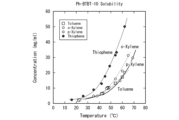
- FIG. 1 shows the solubility curve of 2-decyl-7-phenylbenzothienobenzothiophene in various organic solvents.
- FIG. 2A is a polarizing microscope photograph of a crystal film formed using the organic semiconductor composition of Example 1.
- FIG. 2B is a polarizing microscope photograph of a crystal film formed using the organic semiconductor composition of Comparative Example 1.
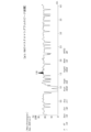
- FIG. 3A shows the results of gas chromatography mass spectrometry of substrate 2.
- FIG. 3B shows the results of gas chromatography mass spectrometry of substrate 1.
- FIG. 3C is an enlarged view of a portion of the results of gas chromatography mass spectrometry of substrate 1.
- FIG. 4 shows the results of X-ray diffraction measurements on the substrates 3, 4, 11 and 12.
- the organic semiconductor composition of the present embodiment includes an organic semiconductor material and a thiophene solvent.
- the thiophene solvent is a solvent containing thiophene as a main component.
- "containing thiophene as a main component” means that the content of thiophene is the highest among the constituent materials of the thiophene solvent.
- the content of thiophene relative to the total amount of the thiophene solvent is 50% or more, preferably 70% or more, more preferably 90% or more, and may be 100%.
- the thiophene solvent may contain other organic compounds within a range that does not impair the effects of the present invention.
- the solvent used for coating organic semiconductors is a non-halogen solvent from the viewpoint of environmental issues and safety for the human body.
- a non-halogen solvent means a solvent that does not contain halogen elements such as F, Cl, or Br.
- Thiophene is a material that is not used as an organic solvent.
- the inventors' research has revealed that organic semiconductor materials that contain compounds with a thiophene ring have high solubility in thiophene.
- Ph-BTBT-10 2-decyl-7-phenylbenzothieneobenzothiophene
- FIG. 1 shows examples in which thiophene, o-xylene, p-xylene, and toluene are used as organic solvents.
- the solubility of Ph-BTBT-10 in thiophene is about 10 mg/ml in the temperature range of 30 to 40° C.
- the solubility of Ph-BTBT-10 in organic solvents other than thiophene is less than 5 mg/ml. That is, it can be confirmed that in the temperature range of 30 to 40° C., the solubility of Ph-BTBT-10 in thiophene is at least about twice as high as that in other organic solvents.
- organic semiconductor thin film using an organic semiconductor composition When forming an organic semiconductor thin film using an organic semiconductor composition, at least 5 mg/ml is required. In the temperature range of 30 to 40°C, organic solvents other than thiophene are saturated, and if you try to adjust the concentration to 5 mg/ml, they will crystallize, making film formation difficult. On the other hand, thiophene has a margin of solubility, so even when adjusted to a concentration of 5 mg/ml, it does not crystallize and film formation is possible at low temperatures.
- the present invention solves these problems by making it possible to prepare highly concentrated organic semiconductor compositions at low temperatures.
- the organic semiconductor material used in this embodiment includes a compound having a thiophene ring.
- compounds having a thiophene ring include thienoacene derivatives having 6 or less rings containing a thiophene ring, such as thieno[3,2-b]thiophene, dinaphthyl[2,3-b:2',3'-f]thieno[3,2-b]thiophene (DNTT), and 2-decyl-7-phenyl[1]benzothieno[3,2-b][1]benzothiophene (BTBT).
- thienoacene derivatives having 6 or less rings containing a thiophene ring such as thieno[3,2-b]thiophene, dinaphthyl[2,3-b:2',3'-f]thieno[3,2-b]thiophene (DNTT), and 2-decyl-7-phenyl[1]benzothieno[3,
- the compound having a thiophene ring is preferably a compound represented by the following formula (1):
- R 1 is an alkyl group having 1 to 16 carbon atoms
- R 2 is an alkyl group having 1 to 16 carbon atoms or an aromatic ring.
- the organic semiconductor material is more preferably a material having liquid crystal properties.
- thiophene organic semiconductor materials having liquid crystal properties include the following.
- the total number of thioacene rings is preferably 6 or less, more preferably 5 or less, and even more preferably 4 or less. If the total number of rings is less than the above upper limit, the solubility in a thiophene solvent is likely to be increased.
- One aspect of the present invention is an organic semiconductor composition
- an organic semiconductor material comprises a compound having a total number of thioacene rings of 6 or less
- the thiophene solvent is a non-halogen solvent and contains thiophene as a main component.
- thiophene derivatives such as chlorothiophene are used as organic solvents (for example, JP 2020-167439 A)
- the embodiment of the present invention which is a compound having a thiophene ring and uses a low molecular weight compound having a total number of rings of 6 or less, is preferable because it further improves the solubility in thiophene solvents.
- a small amount of insulating polymer such as polystyrene may be added to the organic semiconductor composition to control the morphology of the organic semiconductor film to be formed.
- the amount can be appropriately adjusted within the range of 0.1% by mass to 10% by mass relative to the total amount of the organic semiconductor composition.
- the organic semiconductor composition preferably has a concentration of the organic semiconductor material of 0.2% by mass or more, and more preferably 1.0% by mass or more.
- the present embodiment relates to a method for producing an organic semiconductor thin film.
- the method for producing an organic semiconductor thin film of this embodiment includes the steps of preparing an organic semiconductor composition containing an organic semiconductor material and a thiophene solvent, applying the organic semiconductor solution to a substrate, and drying the organic semiconductor solution. Each step will be described below.
- Step of preparing organic semiconductor composition First, an organic semiconductor material containing a compound having a thiophene ring is dissolved in a thiophene solvent to prepare an organic semiconductor composition.
- the organic semiconductor composition is preferably applied to the substrate in one direction.
- a method for applying the organic semiconductor composition for example, other known methods may be used as long as the composition can be applied to the substrate in one direction.
- a spin coating method, a dip coating method, a die coating method, a spray coating method, a roll coating method, a microgravure method, a lip coating method, an inkjet method, an applicator coating method, a brush coating method, etc. may be used.
- the composition may also be applied by a printing method such as flexographic printing or screen printing.
- the thickness of the organic semiconductor film is generally selected depending on the type of device to be produced, such as an organic EL element, optical sensor, solar cell, or transistor.
- the film thickness is set to 5 nm or more and 200 nm or less, more preferably 5 nm or more and 100 nm or less, and even more preferably 5 nm or more and 50 nm or less.
- the thickness of the crystal film to be formed can generally be appropriately controlled by the type of solvent used, the concentration of the organic semiconductor, the type of substrate, the temperature of the organic semiconductor solution, and the temperature of the substrate to which it is applied.
- Ph-BTBT-10 as an organic semiconductor that exhibits liquid crystallinity
- C8-BTBT it is preferable to adjust the film formation temperature to a range of 30°C or higher and 120°C or lower.
- the organic semiconductor composition is applied to a substrate, and a liquid layer of the organic semiconductor composition is formed on the substrate. Furthermore, the thiophene solvent contained in the liquid layer is evaporated and dried, and a solid film of the organic semiconductor is formed on the surface of the substrate.
- the substrate is not particularly limited, and examples of the substrate that can be used include glass, quartz glass, a silicon wafer, a metal plate, and a flexible resin sheet.
- a plastic film can be used as the sheet.
- the plastic film include films made of polyethylene terephthalate (PET), polyethylene naphthalate (PEN), polyethersulfone (PES), polyetherimide, polyetheretherketone, polyphenylene sulfide, polyarylate, polyimide, polycarbonate (PC), cellulose triacetate (TAC), cellulose acetate propionate (CAP), and the like.
- the manufacturing method of this embodiment can form a film by applying a semiconductor solution at a low temperature, so it is not subject to restrictions on the material, size, or shape of the substrate. For this reason, it can also be applied to continuous mass production equipment such as the so-called roll-to-roll process.
- One aspect of the present invention is a method for manufacturing a transistor, comprising a step of forming an organic semiconductor thin film layer using the organic semiconductor composition of the present embodiment.
- This embodiment is a method for manufacturing an electronic device.
- the method for manufacturing an electronic device according to this embodiment includes a step of forming a transistor by the method for manufacturing a transistor according to this embodiment.
- One aspect of the present invention is an organic semiconductor thin film that includes thiophene. Whether or not the organic semiconductor thin film contains thiophene is evaluated by the following method. The substrate having the organic semiconductor thin film is placed in a 100 mL container, sealed, and heated for 60 minutes at 120° C. The gas in the container is collected with a syringe and analyzed by gas chromatography mass spectrometry. If a thiophene peak can be confirmed, the sample is evaluated as "containing thiophene.”
- I d (w/2L) ⁇ C i (V g ⁇ V th ) 2
- L represents the channel length
- w represents the channel width
- ⁇ represents the carrier mobility
- C i represents the capacitance per unit area of the gate insulating layer
- V g represents the gate voltage
- V th represents the threshold voltage.
- Ph-BTBT-10 was synthesized according to a non-patent document (Nature Commun., DOI: 0.1038/ncomms7828). It was then repeatedly purified by silica column chromatography and recrystallization to improve its purity before use.
- Example 1 Ph-BTBT-10 was dissolved in thiophene to prepare a 0.4 mass % Ph-BTBT-10 thiophene solution, which was used as organic semiconductor composition 1.
- An organic semiconductor thin film was produced by applying the organic semiconductor composition 1 to a SiO 2 (300 nm)/Si substrate by spin coating. The spin coating conditions were: liquid temperature of the organic semiconductor composition 1 was 60° C., temperature during spin coating was 40° C., and speed was 3000 rpm for 30 seconds.
- Au was evaporated onto a SiO2 (300 nm)/Si substrate using a shadow mask by vacuum evaporation to form source and drain electrodes, producing a bottom-gate, top-contact type transistor.
- the channel length and channel width were set to 100 ⁇ m and 500 ⁇ m, respectively. Then, thermal annealing was performed at 120° C. for 5 minutes. The characteristics of the produced transistor were examined at room temperature in the atmosphere, and the mobility was calculated from the transistor characteristics in the saturated region by the method described in [Evaluation of carrier mobility] above. The average mobility of the transistors was 3.8 cm 2 /Vs, the highest mobility was 4.1 cm 2 /Vs, and the mobility variation was 7%.
- FIG. 2A is a polarizing microscope photograph of a crystal film formed using the organic semiconductor composition of Example 1. It was confirmed from FIG. 2A that when the organic semiconductor composition of Example 1 was used, there were almost no uneven portions formed by the precipitation of crystal grains due to recrystallization, and a flat film could be formed.
- Ph-BTBT-10 was dissolved in p-xylene to prepare a 0.6 mass % Ph-BTBT-10 p-xylene solution, which was used as organic semiconductor composition 2.
- An organic semiconductor thin film was produced in the same manner as in Example 1, except that Organic Semiconductor Composition 2 was used, and then a transistor was manufactured.
- the average mobility of the transistor measured by the method described in the above [Evaluation of carrier mobility] was 1.4 cm 2 /Vs, the maximum mobility was 1.8 cm 2 /Vs, and the mobility variation was 26%.
- FIG. 2A is a polarizing microscope photograph of a crystal film formed using the organic semiconductor composition of Example 1.
- FIG. 2B is a polarizing microscope photograph of a crystal film formed using the organic semiconductor composition of Comparative Example 1. It was confirmed from FIG. 2A that when the organic semiconductor composition of Example 1 was used, there were almost no crystallized portions and a flat film could be formed. As can be seen from FIG. 2B, when the organic semiconductor composition of Comparative Example 1 was used, crystallized areas were observed, and the substrate was exposed in places, that is, holes were observed in the film.
- Example 1 and Comparative Example 1 confirmed that when thiophene was used as the solvent for the organic semiconductor composition, a flat organic semiconductor thin film could be produced at a film formation temperature of 40°C, and the average mobility was 3.8 cm 2 /Vs, which was comparable to the mobility when the film was formed at a high temperature using p-xylene as the organic solvent.
- Ph-BTBT-10 was dissolved in thiophene to prepare a 0.5% by mass Ph-BTBT-10 thiophene solution, and a film was formed in the same manner as in Example 1, except that organic semiconductor composition 1 was used.
- the thin film that was not thermally annealed was substrate 3, and the thin film that was thermally annealed at 120°C for 5 minutes was substrate 4.
- Ph-BTBT-10 was dissolved in p-xylene to prepare a 0.5% by mass p-xylene solution of Ph-BTBT-10.
- a film was formed in the same manner as in Comparative Example 1, except that organic semiconductor composition 2 was used.
- the thin film that was not thermally annealed was used as substrate 11, and the thin film that was thermally annealed at 120°C for 5 minutes was used as substrate 12.
- Example 1 A 0.5 mass % Ph-BTBT-10 thiophene solution was prepared in the same manner as in Example 1, and used as organic semiconductor composition 3.
- the organic semiconductor composition 3 was applied to a SiO 2 (300 nm)/Si substrate by spin coating.
- the conditions for spin coating were a liquid temperature of the organic semiconductor composition 3 of 60° C. and 3000 rpm for 30 seconds.
- the dimensions of the substrate used at this time were 25 mm ⁇ 20 mm.
- a heat treatment was performed at 120° C. for 5 minutes to produce a substrate 1 provided with an organic semiconductor thin film.
- Test Example 2 A substrate 2 provided with an organic semiconductor thin film was produced in the same manner as in Test Example 1, except that no heat treatment was performed after spin coating.
- the obtained substrates were each placed in a 50 mL container and heated at 120° C. for 60 minutes.
- the gas in the container was collected with a syringe and analyzed by gas chromatography mass spectrometry.
- Thiophene was used as a standard sample.
- the measurement conditions for gas chromatography-mass spectrometry were as follows. ⁇ Column used: HP-5 Heating conditions: 40°C for 4 minutes, heated at 10°C per minute up to 280°C Injection method: splitless Injection port temperature: 250°C Carrier gas: Helium Injection volume: 100 ⁇ l
- Figure 3A shows the results for substrate 2
- Figures 3B and 3C show the results for substrate 1.
- Figure 3C is an enlarged view of a portion of Figure 3B.
- a peak was observed at a retention time of about 1.7 minutes. Therefore, the peak at about 1.7 minutes is the peak of thiophene.
- 3A, 3B, and 3C a peak was observed at a retention time of about 1.7 minutes. This confirmed that when thiophene was used as a solvent for the organic semiconductor composition, the produced organic semiconductor thin film contained thiophene.
- test examples 1 to 3 confirmed that transistors with little variation in mobility can be manufactured even when thiophene solvent is used.
Landscapes
- Engineering & Computer Science (AREA)
- Manufacturing & Machinery (AREA)
- Physics & Mathematics (AREA)
- Spectroscopy & Molecular Physics (AREA)
- Chemical & Material Sciences (AREA)
- Materials Engineering (AREA)
- Thin Film Transistor (AREA)
Abstract
L'invention concerne une composition semi-conductrice organique contenant un matériau semi-conducteur organique et un solvant thiophène, le matériau semi-conducteur organique contenant un composé ayant un cycle thiophène; et le solvant thiophène contenant du thiophène en tant que composant principal. Il est préférable que le matériau semi-conducteur organique ait une cristallinité liquide, et il est également préférable que le solvant thiophène soit un solvant non halogéné.
Applications Claiming Priority (2)
| Application Number | Priority Date | Filing Date | Title |
|---|---|---|---|
| JP2023097654 | 2023-06-14 | ||
| JP2023-097654 | 2023-06-14 |
Publications (1)
| Publication Number | Publication Date |
|---|---|
| WO2024257469A1 true WO2024257469A1 (fr) | 2024-12-19 |
Family
ID=93851936
Family Applications (1)
| Application Number | Title | Priority Date | Filing Date |
|---|---|---|---|
| PCT/JP2024/014936 Ceased WO2024257469A1 (fr) | 2023-06-14 | 2024-04-15 | Composition semi-conductrice organique, procédé de fabrication de transistor, film mince semi-conducteur organique et transistor |
Country Status (2)
| Country | Link |
|---|---|
| TW (1) | TW202502776A (fr) |
| WO (1) | WO2024257469A1 (fr) |
Citations (2)
| Publication number | Priority date | Publication date | Assignee | Title |
|---|---|---|---|---|
| WO2018061691A1 (fr) * | 2016-09-27 | 2018-04-05 | 富士フイルム株式会社 | Procédé de production d'un film |
| WO2022244847A1 (fr) * | 2021-05-20 | 2022-11-24 | 国立大学法人東京工業大学 | Film mince à semi-conducteur organique, transistor, procédé de fabrication de film mince à semi-conducteur organique, procédé de fabrication de transistor et procédé de fabrication de dispositif électronique |
-
2024
- 2024-04-15 WO PCT/JP2024/014936 patent/WO2024257469A1/fr not_active Ceased
- 2024-05-16 TW TW113118128A patent/TW202502776A/zh unknown
Patent Citations (2)
| Publication number | Priority date | Publication date | Assignee | Title |
|---|---|---|---|---|
| WO2018061691A1 (fr) * | 2016-09-27 | 2018-04-05 | 富士フイルム株式会社 | Procédé de production d'un film |
| WO2022244847A1 (fr) * | 2021-05-20 | 2022-11-24 | 国立大学法人東京工業大学 | Film mince à semi-conducteur organique, transistor, procédé de fabrication de film mince à semi-conducteur organique, procédé de fabrication de transistor et procédé de fabrication de dispositif électronique |
Also Published As
| Publication number | Publication date |
|---|---|
| TW202502776A (zh) | 2025-01-16 |
Similar Documents
| Publication | Publication Date | Title |
|---|---|---|
| EP2077590B1 (fr) | Transistor à effet de champ | |
| Chen et al. | Understanding the meniscus‐guided coating parameters in organic field‐effect‐transistor fabrications | |
| US20080048185A1 (en) | Field effect transistor and method of manufacturing the same | |
| KR102001455B1 (ko) | 반도체 조성물 | |
| JP5160078B2 (ja) | 電界効果トランジスタ | |
| WO2013024678A1 (fr) | Composé permettant de former un film monomoléculaire auto-assemblé, et élément semi-conducteur organique le contenant | |
| US20240090243A1 (en) | Organic semiconductor thin film, transistor, method for producing organic semiconductor thin film, method for producing transistor, and method for producing electronic device | |
| CN102770979B (zh) | 有机半导体材料和场效应晶体管以及场效应晶体管的制造方法 | |
| JP2012044109A (ja) | 電界効果トランジスタ及びその製造方法 | |
| US20140264314A1 (en) | Method for manufacturing organic semiconductor element, semiconductor element, and electronic apparatus | |
| US20200168806A1 (en) | Compound and organic thin film and thin film transistor and electronic device | |
| Park et al. | Self-assembly of organic channel/polymer dielectric layer in solution process for low-voltage thin-film transistors | |
| JP5428113B2 (ja) | 電界効果トランジスタ | |
| KR20160055334A (ko) | 유기 전계 효과 트랜지스터의 제조방법 | |
| TW202502776A (zh) | 有機半導體組成物、電晶體之製造方法、有機半導體薄膜及電晶體 | |
| KR20140027391A (ko) | 재료의 배향 결정화 방법 | |
| EP3471160B1 (fr) | Composition pour la production de dispositifs semiconducteurs organiques | |
| WO2014136942A1 (fr) | Procédé de formation de couche mince organique | |
| US7863081B2 (en) | Field effect transistor and method of manufacturing the same | |
| JP4868825B2 (ja) | 有機系電界効果トランジスタ | |
| JP7741493B2 (ja) | 有機半導体材料及びその用途 | |
| JP6214938B2 (ja) | 有機半導体及びその用途、並びに半導体層形成用インク | |
| EP3845525B1 (fr) | Composé organique contenant un chalcogène, matériau semi-conducteur organique, film semi-conducteur organique et transistor à effet de champ organique | |
| JP2007266201A (ja) | 電界効果トランジスタ | |
| JP2008053659A (ja) | 高品位分子性結晶製造方法及び有機半導体デバイス |
Legal Events
| Date | Code | Title | Description |
|---|---|---|---|
| 121 | Ep: the epo has been informed by wipo that ep was designated in this application |
Ref document number: 24823091 Country of ref document: EP Kind code of ref document: A1 |
|
| NENP | Non-entry into the national phase |
Ref country code: DE |