WO2024257469A1 - 有機半導体組成物、トランジスタの製造方法、有機半導体薄膜及びトランジスタ - Google Patents
有機半導体組成物、トランジスタの製造方法、有機半導体薄膜及びトランジスタ Download PDFInfo
- Publication number
- WO2024257469A1 WO2024257469A1 PCT/JP2024/014936 JP2024014936W WO2024257469A1 WO 2024257469 A1 WO2024257469 A1 WO 2024257469A1 JP 2024014936 W JP2024014936 W JP 2024014936W WO 2024257469 A1 WO2024257469 A1 WO 2024257469A1
- Authority
- WO
- WIPO (PCT)
- Prior art keywords
- organic semiconductor
- thiophene
- solvent
- transistor
- thin film
- Prior art date
- Legal status (The legal status is an assumption and is not a legal conclusion. Google has not performed a legal analysis and makes no representation as to the accuracy of the status listed.)
- Ceased
Links
Images



Classifications
-
- H—ELECTRICITY
- H10—SEMICONDUCTOR DEVICES; ELECTRIC SOLID-STATE DEVICES NOT OTHERWISE PROVIDED FOR
- H10K—ORGANIC ELECTRIC SOLID-STATE DEVICES
- H10K10/00—Organic devices specially adapted for rectifying, amplifying, oscillating or switching; Organic capacitors or resistors having potential barriers
- H10K10/40—Organic transistors
- H10K10/46—Field-effect transistors, e.g. organic thin-film transistors [OTFT]
-
- H—ELECTRICITY
- H10—SEMICONDUCTOR DEVICES; ELECTRIC SOLID-STATE DEVICES NOT OTHERWISE PROVIDED FOR
- H10K—ORGANIC ELECTRIC SOLID-STATE DEVICES
- H10K71/00—Manufacture or treatment specially adapted for the organic devices covered by this subclass
- H10K71/10—Deposition of organic active material
- H10K71/12—Deposition of organic active material using liquid deposition, e.g. spin coating
- H10K71/15—Deposition of organic active material using liquid deposition, e.g. spin coating characterised by the solvent used
-
- H—ELECTRICITY
- H10—SEMICONDUCTOR DEVICES; ELECTRIC SOLID-STATE DEVICES NOT OTHERWISE PROVIDED FOR
- H10K—ORGANIC ELECTRIC SOLID-STATE DEVICES
- H10K85/00—Organic materials used in the body or electrodes of devices covered by this subclass
- H10K85/60—Organic compounds having low molecular weight
Definitions
- the present invention relates to an organic semiconductor composition, a method for producing a transistor, an organic semiconductor thin film, and a transistor.
- a known method for manufacturing an organic semiconductor thin film is to apply a composition containing an organic semiconductor compound and a solvent to a substrate and then evaporate the solvent to form an organic semiconductor thin film.
- Patent Document 1 discloses a condensed polycyclic aromatic compound having a [1]benzothieno[3,2-b][1]benzothiophene skeleton as an organic semiconductor compound that exhibits high carrier mobility.
- Low-temperature film-forming process refers to a process that includes a step in which the film-forming temperature for the organic semiconductor thin film is set to 60°C or lower.
- the organic semiconductor composition of the present invention includes an organic semiconductor material and a thiophene solvent.
- the organic semiconductor material includes a compound having a thiophene ring, and the thiophene solvent includes thiophene as a main component.
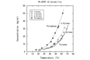
- FIG. 1 shows the solubility curve of 2-decyl-7-phenylbenzothienobenzothiophene in various organic solvents.
- FIG. 2A is a polarizing microscope photograph of a crystal film formed using the organic semiconductor composition of Example 1.
- FIG. 2B is a polarizing microscope photograph of a crystal film formed using the organic semiconductor composition of Comparative Example 1.
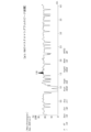
- FIG. 3A shows the results of gas chromatography mass spectrometry of substrate 2.
- FIG. 3B shows the results of gas chromatography mass spectrometry of substrate 1.
- FIG. 3C is an enlarged view of a portion of the results of gas chromatography mass spectrometry of substrate 1.
- FIG. 4 shows the results of X-ray diffraction measurements on the substrates 3, 4, 11 and 12.
- the organic semiconductor composition of the present embodiment includes an organic semiconductor material and a thiophene solvent.
- the thiophene solvent is a solvent containing thiophene as a main component.
- "containing thiophene as a main component” means that the content of thiophene is the highest among the constituent materials of the thiophene solvent.
- the content of thiophene relative to the total amount of the thiophene solvent is 50% or more, preferably 70% or more, more preferably 90% or more, and may be 100%.
- the thiophene solvent may contain other organic compounds within a range that does not impair the effects of the present invention.
- the solvent used for coating organic semiconductors is a non-halogen solvent from the viewpoint of environmental issues and safety for the human body.
- a non-halogen solvent means a solvent that does not contain halogen elements such as F, Cl, or Br.
- Thiophene is a material that is not used as an organic solvent.
- the inventors' research has revealed that organic semiconductor materials that contain compounds with a thiophene ring have high solubility in thiophene.
- Ph-BTBT-10 2-decyl-7-phenylbenzothieneobenzothiophene
- FIG. 1 shows examples in which thiophene, o-xylene, p-xylene, and toluene are used as organic solvents.
- the solubility of Ph-BTBT-10 in thiophene is about 10 mg/ml in the temperature range of 30 to 40° C.
- the solubility of Ph-BTBT-10 in organic solvents other than thiophene is less than 5 mg/ml. That is, it can be confirmed that in the temperature range of 30 to 40° C., the solubility of Ph-BTBT-10 in thiophene is at least about twice as high as that in other organic solvents.
- organic semiconductor thin film using an organic semiconductor composition When forming an organic semiconductor thin film using an organic semiconductor composition, at least 5 mg/ml is required. In the temperature range of 30 to 40°C, organic solvents other than thiophene are saturated, and if you try to adjust the concentration to 5 mg/ml, they will crystallize, making film formation difficult. On the other hand, thiophene has a margin of solubility, so even when adjusted to a concentration of 5 mg/ml, it does not crystallize and film formation is possible at low temperatures.
- the present invention solves these problems by making it possible to prepare highly concentrated organic semiconductor compositions at low temperatures.
- the organic semiconductor material used in this embodiment includes a compound having a thiophene ring.
- compounds having a thiophene ring include thienoacene derivatives having 6 or less rings containing a thiophene ring, such as thieno[3,2-b]thiophene, dinaphthyl[2,3-b:2',3'-f]thieno[3,2-b]thiophene (DNTT), and 2-decyl-7-phenyl[1]benzothieno[3,2-b][1]benzothiophene (BTBT).
- thienoacene derivatives having 6 or less rings containing a thiophene ring such as thieno[3,2-b]thiophene, dinaphthyl[2,3-b:2',3'-f]thieno[3,2-b]thiophene (DNTT), and 2-decyl-7-phenyl[1]benzothieno[3,
- the compound having a thiophene ring is preferably a compound represented by the following formula (1):
- R 1 is an alkyl group having 1 to 16 carbon atoms
- R 2 is an alkyl group having 1 to 16 carbon atoms or an aromatic ring.
- the organic semiconductor material is more preferably a material having liquid crystal properties.
- thiophene organic semiconductor materials having liquid crystal properties include the following.
- the total number of thioacene rings is preferably 6 or less, more preferably 5 or less, and even more preferably 4 or less. If the total number of rings is less than the above upper limit, the solubility in a thiophene solvent is likely to be increased.
- One aspect of the present invention is an organic semiconductor composition
- an organic semiconductor material comprises a compound having a total number of thioacene rings of 6 or less
- the thiophene solvent is a non-halogen solvent and contains thiophene as a main component.
- thiophene derivatives such as chlorothiophene are used as organic solvents (for example, JP 2020-167439 A)
- the embodiment of the present invention which is a compound having a thiophene ring and uses a low molecular weight compound having a total number of rings of 6 or less, is preferable because it further improves the solubility in thiophene solvents.
- a small amount of insulating polymer such as polystyrene may be added to the organic semiconductor composition to control the morphology of the organic semiconductor film to be formed.
- the amount can be appropriately adjusted within the range of 0.1% by mass to 10% by mass relative to the total amount of the organic semiconductor composition.
- the organic semiconductor composition preferably has a concentration of the organic semiconductor material of 0.2% by mass or more, and more preferably 1.0% by mass or more.
- the present embodiment relates to a method for producing an organic semiconductor thin film.
- the method for producing an organic semiconductor thin film of this embodiment includes the steps of preparing an organic semiconductor composition containing an organic semiconductor material and a thiophene solvent, applying the organic semiconductor solution to a substrate, and drying the organic semiconductor solution. Each step will be described below.
- Step of preparing organic semiconductor composition First, an organic semiconductor material containing a compound having a thiophene ring is dissolved in a thiophene solvent to prepare an organic semiconductor composition.
- the organic semiconductor composition is preferably applied to the substrate in one direction.
- a method for applying the organic semiconductor composition for example, other known methods may be used as long as the composition can be applied to the substrate in one direction.
- a spin coating method, a dip coating method, a die coating method, a spray coating method, a roll coating method, a microgravure method, a lip coating method, an inkjet method, an applicator coating method, a brush coating method, etc. may be used.
- the composition may also be applied by a printing method such as flexographic printing or screen printing.
- the thickness of the organic semiconductor film is generally selected depending on the type of device to be produced, such as an organic EL element, optical sensor, solar cell, or transistor.
- the film thickness is set to 5 nm or more and 200 nm or less, more preferably 5 nm or more and 100 nm or less, and even more preferably 5 nm or more and 50 nm or less.
- the thickness of the crystal film to be formed can generally be appropriately controlled by the type of solvent used, the concentration of the organic semiconductor, the type of substrate, the temperature of the organic semiconductor solution, and the temperature of the substrate to which it is applied.
- Ph-BTBT-10 as an organic semiconductor that exhibits liquid crystallinity
- C8-BTBT it is preferable to adjust the film formation temperature to a range of 30°C or higher and 120°C or lower.
- the organic semiconductor composition is applied to a substrate, and a liquid layer of the organic semiconductor composition is formed on the substrate. Furthermore, the thiophene solvent contained in the liquid layer is evaporated and dried, and a solid film of the organic semiconductor is formed on the surface of the substrate.
- the substrate is not particularly limited, and examples of the substrate that can be used include glass, quartz glass, a silicon wafer, a metal plate, and a flexible resin sheet.
- a plastic film can be used as the sheet.
- the plastic film include films made of polyethylene terephthalate (PET), polyethylene naphthalate (PEN), polyethersulfone (PES), polyetherimide, polyetheretherketone, polyphenylene sulfide, polyarylate, polyimide, polycarbonate (PC), cellulose triacetate (TAC), cellulose acetate propionate (CAP), and the like.
- the manufacturing method of this embodiment can form a film by applying a semiconductor solution at a low temperature, so it is not subject to restrictions on the material, size, or shape of the substrate. For this reason, it can also be applied to continuous mass production equipment such as the so-called roll-to-roll process.
- One aspect of the present invention is a method for manufacturing a transistor, comprising a step of forming an organic semiconductor thin film layer using the organic semiconductor composition of the present embodiment.
- This embodiment is a method for manufacturing an electronic device.
- the method for manufacturing an electronic device according to this embodiment includes a step of forming a transistor by the method for manufacturing a transistor according to this embodiment.
- One aspect of the present invention is an organic semiconductor thin film that includes thiophene. Whether or not the organic semiconductor thin film contains thiophene is evaluated by the following method. The substrate having the organic semiconductor thin film is placed in a 100 mL container, sealed, and heated for 60 minutes at 120° C. The gas in the container is collected with a syringe and analyzed by gas chromatography mass spectrometry. If a thiophene peak can be confirmed, the sample is evaluated as "containing thiophene.”
- I d (w/2L) ⁇ C i (V g ⁇ V th ) 2
- L represents the channel length
- w represents the channel width
- ⁇ represents the carrier mobility
- C i represents the capacitance per unit area of the gate insulating layer
- V g represents the gate voltage
- V th represents the threshold voltage.
- Ph-BTBT-10 was synthesized according to a non-patent document (Nature Commun., DOI: 0.1038/ncomms7828). It was then repeatedly purified by silica column chromatography and recrystallization to improve its purity before use.
- Example 1 Ph-BTBT-10 was dissolved in thiophene to prepare a 0.4 mass % Ph-BTBT-10 thiophene solution, which was used as organic semiconductor composition 1.
- An organic semiconductor thin film was produced by applying the organic semiconductor composition 1 to a SiO 2 (300 nm)/Si substrate by spin coating. The spin coating conditions were: liquid temperature of the organic semiconductor composition 1 was 60° C., temperature during spin coating was 40° C., and speed was 3000 rpm for 30 seconds.
- Au was evaporated onto a SiO2 (300 nm)/Si substrate using a shadow mask by vacuum evaporation to form source and drain electrodes, producing a bottom-gate, top-contact type transistor.
- the channel length and channel width were set to 100 ⁇ m and 500 ⁇ m, respectively. Then, thermal annealing was performed at 120° C. for 5 minutes. The characteristics of the produced transistor were examined at room temperature in the atmosphere, and the mobility was calculated from the transistor characteristics in the saturated region by the method described in [Evaluation of carrier mobility] above. The average mobility of the transistors was 3.8 cm 2 /Vs, the highest mobility was 4.1 cm 2 /Vs, and the mobility variation was 7%.
- FIG. 2A is a polarizing microscope photograph of a crystal film formed using the organic semiconductor composition of Example 1. It was confirmed from FIG. 2A that when the organic semiconductor composition of Example 1 was used, there were almost no uneven portions formed by the precipitation of crystal grains due to recrystallization, and a flat film could be formed.
- Ph-BTBT-10 was dissolved in p-xylene to prepare a 0.6 mass % Ph-BTBT-10 p-xylene solution, which was used as organic semiconductor composition 2.
- An organic semiconductor thin film was produced in the same manner as in Example 1, except that Organic Semiconductor Composition 2 was used, and then a transistor was manufactured.
- the average mobility of the transistor measured by the method described in the above [Evaluation of carrier mobility] was 1.4 cm 2 /Vs, the maximum mobility was 1.8 cm 2 /Vs, and the mobility variation was 26%.
- FIG. 2A is a polarizing microscope photograph of a crystal film formed using the organic semiconductor composition of Example 1.
- FIG. 2B is a polarizing microscope photograph of a crystal film formed using the organic semiconductor composition of Comparative Example 1. It was confirmed from FIG. 2A that when the organic semiconductor composition of Example 1 was used, there were almost no crystallized portions and a flat film could be formed. As can be seen from FIG. 2B, when the organic semiconductor composition of Comparative Example 1 was used, crystallized areas were observed, and the substrate was exposed in places, that is, holes were observed in the film.
- Example 1 and Comparative Example 1 confirmed that when thiophene was used as the solvent for the organic semiconductor composition, a flat organic semiconductor thin film could be produced at a film formation temperature of 40°C, and the average mobility was 3.8 cm 2 /Vs, which was comparable to the mobility when the film was formed at a high temperature using p-xylene as the organic solvent.
- Ph-BTBT-10 was dissolved in thiophene to prepare a 0.5% by mass Ph-BTBT-10 thiophene solution, and a film was formed in the same manner as in Example 1, except that organic semiconductor composition 1 was used.
- the thin film that was not thermally annealed was substrate 3, and the thin film that was thermally annealed at 120°C for 5 minutes was substrate 4.
- Ph-BTBT-10 was dissolved in p-xylene to prepare a 0.5% by mass p-xylene solution of Ph-BTBT-10.
- a film was formed in the same manner as in Comparative Example 1, except that organic semiconductor composition 2 was used.
- the thin film that was not thermally annealed was used as substrate 11, and the thin film that was thermally annealed at 120°C for 5 minutes was used as substrate 12.
- Example 1 A 0.5 mass % Ph-BTBT-10 thiophene solution was prepared in the same manner as in Example 1, and used as organic semiconductor composition 3.
- the organic semiconductor composition 3 was applied to a SiO 2 (300 nm)/Si substrate by spin coating.
- the conditions for spin coating were a liquid temperature of the organic semiconductor composition 3 of 60° C. and 3000 rpm for 30 seconds.
- the dimensions of the substrate used at this time were 25 mm ⁇ 20 mm.
- a heat treatment was performed at 120° C. for 5 minutes to produce a substrate 1 provided with an organic semiconductor thin film.
- Test Example 2 A substrate 2 provided with an organic semiconductor thin film was produced in the same manner as in Test Example 1, except that no heat treatment was performed after spin coating.
- the obtained substrates were each placed in a 50 mL container and heated at 120° C. for 60 minutes.
- the gas in the container was collected with a syringe and analyzed by gas chromatography mass spectrometry.
- Thiophene was used as a standard sample.
- the measurement conditions for gas chromatography-mass spectrometry were as follows. ⁇ Column used: HP-5 Heating conditions: 40°C for 4 minutes, heated at 10°C per minute up to 280°C Injection method: splitless Injection port temperature: 250°C Carrier gas: Helium Injection volume: 100 ⁇ l
- Figure 3A shows the results for substrate 2
- Figures 3B and 3C show the results for substrate 1.
- Figure 3C is an enlarged view of a portion of Figure 3B.
- a peak was observed at a retention time of about 1.7 minutes. Therefore, the peak at about 1.7 minutes is the peak of thiophene.
- 3A, 3B, and 3C a peak was observed at a retention time of about 1.7 minutes. This confirmed that when thiophene was used as a solvent for the organic semiconductor composition, the produced organic semiconductor thin film contained thiophene.
- test examples 1 to 3 confirmed that transistors with little variation in mobility can be manufactured even when thiophene solvent is used.
Landscapes
- Engineering & Computer Science (AREA)
- Manufacturing & Machinery (AREA)
- Physics & Mathematics (AREA)
- Spectroscopy & Molecular Physics (AREA)
- Chemical & Material Sciences (AREA)
- Materials Engineering (AREA)
- Thin Film Transistor (AREA)
Abstract
有機半導体材料とチオフェン溶媒とを含む有機半導体組成物であって、前記有機半導体材料はチオフェン環を有する化合物を含み、前記チオフェン溶媒は主成分としてチオフェンを含む溶媒である、有機半導体組成物。有機半導体材料は液晶性を有することが好ましく、チオフェン溶媒は非ハロゲン溶媒であることが好ましい。
Description
本発明は、有機半導体組成物、トランジスタの製造方法、有機半導体薄膜及びトランジスタに関する。
本願は、2023年6月14日に、日本に出願された特願2023-097654号に基づき優先権を主張し、その内容をここに援用する。
本願は、2023年6月14日に、日本に出願された特願2023-097654号に基づき優先権を主張し、その内容をここに援用する。
有機半導体薄膜を製造する方法として、有機半導体化合物と溶媒を含む組成物を基板に塗布し、溶媒を蒸発させて有機半導体薄膜を形成する方法が知られている。
例えば特許文献1は、高いキャリア移動度を示す有機半導体化合物として、[1]ベンゾチエノ[3,2-b][1]ベンゾチオフェン骨格を有する縮合多環芳香族化合物を開示している。
有機半導体薄膜の製造においては、高いキャリア移動度、低温での成膜プロセスへの適用性などの諸特性が求められ、さらにこれらの特性の値のばらつきが少ないことが要求される。「低温での成膜プロセス」とは、有機半導体薄膜の成膜温度を60℃以下の温度とする工程を備えるプロセスを意味する。
本発明の有機半導体組成物は、有機半導体材料とチオフェン溶媒とを含む。有機半導体材料はチオフェン環を有する化合物を含み、チオフェン溶媒は主成分としてチオフェンを含む。
<有機半導体組成物>
本実施形態の有機半導体組成物は、有機半導体材料とチオフェン溶媒とを含む。
チオフェン溶媒は主成分としてチオフェンを含む溶媒である。ここで「主成分としてチオフェンを含む」とは、チオフェン溶媒の構成材料のうち、チオフェンの含有率が最も多いことを意味する。チオフェン溶媒の全量に対するチオフェンの含有率は、50%以上であり、70%以上が好ましく、90%以上がより好ましく、100%であってもよい。 チオフェン溶媒は、本発明の効果を損なわない範囲で他の有機化合物を含んでいてもよい。
本実施形態の有機半導体組成物は、有機半導体材料とチオフェン溶媒とを含む。
チオフェン溶媒は主成分としてチオフェンを含む溶媒である。ここで「主成分としてチオフェンを含む」とは、チオフェン溶媒の構成材料のうち、チオフェンの含有率が最も多いことを意味する。チオフェン溶媒の全量に対するチオフェンの含有率は、50%以上であり、70%以上が好ましく、90%以上がより好ましく、100%であってもよい。 チオフェン溶媒は、本発明の効果を損なわない範囲で他の有機化合物を含んでいてもよい。
一般に有機半導体の塗布に用いる溶媒は、環境問題や人体への安全性の観点から、非ハロゲン溶媒であることが好ましい。非ハロゲン溶媒とは、F、Cl、Br等のハロゲン元素を含まない溶媒を意味する。
チオフェンは有機溶媒としては利用されない材料である。本発明者らの検討によりチオフェン環を有する化合物を含む有機半導体材料は、チオフェンに対して高い溶解性を有することが見いだされた。
図1に、各有機溶媒に対する、2-decyl-7-phenylbenzothieneobenzothiophene(以下、「Ph-BTBT-10」と記載する)の溶解度曲線を示す。Ph-BTBT-10は、チオフェン環を有する化合物を含む有機半導体材料の一例である。
図1には、有機溶媒としてチオフェン、o-キシレン、p-キシレン及びトルエンを用いた例をそれぞれ記載する。
図1には、有機溶媒としてチオフェン、o-キシレン、p-キシレン及びトルエンを用いた例をそれぞれ記載する。
図1から、30~40℃の温度範囲において、チオフェンに対するPh-BTBT-10の溶解度は約10mg/mlであることが確認できる。
一方、チオフェン以外の有機溶媒に対するPh-BTBT-10の溶解度は5mg/mlを下回ることが確認できる。
即ち、30~40℃の温度範囲において、チオフェンに対するPh-BTBT-10の溶解度は、他の有機溶媒よりも少なくとも約2倍であること確認できる。
一方、チオフェン以外の有機溶媒に対するPh-BTBT-10の溶解度は5mg/mlを下回ることが確認できる。
即ち、30~40℃の温度範囲において、チオフェンに対するPh-BTBT-10の溶解度は、他の有機溶媒よりも少なくとも約2倍であること確認できる。
有機半導体組成物を用いて有機半導体薄膜を成膜する際には、少なくとも5mg/mlは必要である。30~40℃の温度範囲において、チオフェン以外の有機溶媒は飽和状態であり、5mg/mlの濃度に調整しようとすると結晶化してしまい、成膜が困難となる。一方チオフェンは溶解度に余裕があるため、5mg/mlの濃度に調整した場合でも結晶化することなく、低温での成膜が可能である。
図1の結果から、チオフェンを使用すると40℃以下の低温範囲においても高濃度の有機半導体組成物を調製できることが見いだされた。
有機半導体組成物の溶解度を向上するアプローチとしては、有機溶媒の温度を上昇させる方法があるが、可燃性の溶媒を加熱することは安全性の観点から問題がある。
また、有機溶媒の温度を上昇させると濃度も上昇するものの、有機半導体組成物の粘度が低下し、塗布しにくくなるという問題も生じる。
有機半導体組成物の溶解度を向上するアプローチとしては、有機溶媒の温度を上昇させる方法があるが、可燃性の溶媒を加熱することは安全性の観点から問題がある。
また、有機溶媒の温度を上昇させると濃度も上昇するものの、有機半導体組成物の粘度が低下し、塗布しにくくなるという問題も生じる。
本発明は低温範囲において高濃度の有機半導体組成物を調製できるため、このような問題を解決している。
≪有機半導体材料≫
本実施形態に用いる有機半導体材料は、チオフェン環を有する化合物を含む。
チオフェン環を有する化合物としては、チエノ[3,2-b]チオフェン、ジナフチル[2,3-b:2’,3’-f]チエノ[3,2-b]チオフェン(DNTT)、2-デシル-7-フェニル[1]ベンゾチエノ[3,2-b][1]ベンゾチオフェン(BTBT)等のチオフェン環を含む環数6以下のチエノアセン誘導体が挙げられる。
本実施形態に用いる有機半導体材料は、チオフェン環を有する化合物を含む。
チオフェン環を有する化合物としては、チエノ[3,2-b]チオフェン、ジナフチル[2,3-b:2’,3’-f]チエノ[3,2-b]チオフェン(DNTT)、2-デシル-7-フェニル[1]ベンゾチエノ[3,2-b][1]ベンゾチオフェン(BTBT)等のチオフェン環を含む環数6以下のチエノアセン誘導体が挙げられる。
チオフェン環を有する化合物は、下記式(1)で表される化合物が好ましい。

式(1)中、R1は炭素数1~16のアルキル基であり、R2は炭素数1~16のアルキル基又は芳香環である。
液晶材料に限定しないものの、有機半導体材料は液晶性を有する材料であることがさらに好ましい。
液晶性を有するチオフェン有機半導体材料として、以下が挙げられる。
液晶性を有するチオフェン有機半導体材料として、以下が挙げられる。

チオフェン環を有する化合物は、チオアセンの総環数が6以下であることが好ましく、5以下であることがより好ましく、4以下であることがさらに好ましい。総環数が上記上限値以下であると、チオフェン溶媒に対する溶解度が高まりやすい。
本発明の一態様は、有機半導体材料とチオフェン溶媒とを含む有機半導体組成物であって、有機半導体材料は、チオアセンの総環数が6以下の化合物を含み、チオフェン溶媒は非ハロゲン溶媒であり、主成分としてチオフェンを含む、有機半導体組成物である。
化学構造が類似する物質同士は、溶解度が高くなることが知られている。しかし、チオフェンは、クロロチオフェン等のチオフェン誘導体が有機溶媒として使用されている例(例えば特開2020-167439号公報)はあるものの、チオフェンを有機溶媒として使用した例はなかった。本発明の一態様である、チオフェン環を有する化合物であって、総環数が6以下の低分子量化合物を使用する態様は、チオフェン溶媒への溶解性がより向上するため好ましい。
化学構造が類似する物質同士は、溶解度が高くなることが知られている。しかし、チオフェンは、クロロチオフェン等のチオフェン誘導体が有機溶媒として使用されている例(例えば特開2020-167439号公報)はあるものの、チオフェンを有機溶媒として使用した例はなかった。本発明の一態様である、チオフェン環を有する化合物であって、総環数が6以下の低分子量化合物を使用する態様は、チオフェン溶媒への溶解性がより向上するため好ましい。
有機半導体組成物は、形成する有機半導体膜のモフォロジーの制御のため、ポリスチレンなどの絶縁性のポリマーを少量添加してもよい。絶縁性のポリマーを添加する場合には、有機半導体組成物の全量に対し、0.1質量%以上10質量%以下の範囲で適宜調整できる。
有機半導体組成物は、有機半導体材料の濃度が0.2質量%以上であることが好ましく、1.0質量%以上であることがより好ましい。
<有機半導体薄膜の製造方法>
本実施形態は、有機半導体薄膜の製造方法に関する。
本実施形態の有機半導体薄膜の製造方法は、有機半導体材料とチオフェン溶媒とを含む有機半導体組成物を調製する工程と、有機半導体溶液を基材に塗布する工程と、有機半導体溶液を乾燥する工程と、を有する。
以下、各工程について説明する。
本実施形態は、有機半導体薄膜の製造方法に関する。
本実施形態の有機半導体薄膜の製造方法は、有機半導体材料とチオフェン溶媒とを含む有機半導体組成物を調製する工程と、有機半導体溶液を基材に塗布する工程と、有機半導体溶液を乾燥する工程と、を有する。
以下、各工程について説明する。
[有機半導体組成物を調製する工程]
まず、チオフェン環を有する化合物を含む有機半導体材料をチオフェン溶媒に溶解し、有機半導体組成物を調製する。
まず、チオフェン環を有する化合物を含む有機半導体材料をチオフェン溶媒に溶解し、有機半導体組成物を調製する。
[塗布する工程]
次に、塗布方法に応じて、基材に有機半導体溶液の液膜を形成する。
本実施形態において、有機半導体組成物は基材に対して一方向に塗布されることが好ましい。有機半導体組成物を塗布する方法としては、例えば、塗布方法としては、基材に対して一方向に塗布可能であれば他の公知の方法を用いてもよい。例えば、スピンコート法、ディップコート法、ダイコート法、スプレーコート法、ロールコート法、マイクログラビア法、リップコート法、インクジェット法、アプリケーター塗布、刷毛塗り等の塗布方法が使用できる。また、フレキソ印刷、スクリーン印刷等の印刷法により塗布してもよい。
次に、塗布方法に応じて、基材に有機半導体溶液の液膜を形成する。
本実施形態において、有機半導体組成物は基材に対して一方向に塗布されることが好ましい。有機半導体組成物を塗布する方法としては、例えば、塗布方法としては、基材に対して一方向に塗布可能であれば他の公知の方法を用いてもよい。例えば、スピンコート法、ディップコート法、ダイコート法、スプレーコート法、ロールコート法、マイクログラビア法、リップコート法、インクジェット法、アプリケーター塗布、刷毛塗り等の塗布方法が使用できる。また、フレキソ印刷、スクリーン印刷等の印刷法により塗布してもよい。
有機半導体膜厚は一般に、有機EL素子、光センサ、太陽電池、トランジスタ等、作製するデバイスの種類により選ばれる。例えば、有機トランジスタを作製する場合は、その膜厚は5nm以上200nm以下、より好ましくは5nm以上100nm以下、さらに好ましくは5nm以上50nm以下に設定する。作製する結晶膜の膜厚は基材に塗布する液膜の厚さにより直接、制御することも可能である。また、一般に、用いる溶媒の種類、有機半導体の濃度、基材の種類や有機半導体溶液の温度、塗布される基材の温度によって形成する結晶膜の厚さは適宜制御できる。
例えば、液晶性を発現する有機半導体としてPh-BTBT-10を用いる場合、成膜温度を40℃以上150℃以下の範囲に調整することが好ましい。また、C8-BTBTを用いる場合には、成膜温度を30℃以上120℃以下の範囲に調整することが好ましい。
[有機半導体溶液を乾燥する工程]
本実施形態の製造方法においては、基材に有機半導体組成物を塗布するとともに有機半導体組成物の液層が基材に形成される。さらに、液層に含まれるチオフェン溶媒が蒸発により乾燥し、基材の表面に有機半導体の固体膜が成膜される。
本実施形態の製造方法においては、基材に有機半導体組成物を塗布するとともに有機半導体組成物の液層が基材に形成される。さらに、液層に含まれるチオフェン溶媒が蒸発により乾燥し、基材の表面に有機半導体の固体膜が成膜される。
基材としては、特に限定されず、ガラス、石英ガラス、シリコンウェハ、金属板、フレキシブルな樹脂製シートを用いることができる。
例えば、プラスチックフィルムをシートとして用いることができる。前記プラスチックフィルムとしては、例えば、ポリエチレンテレフタレート(PET)、ポリエチレンナフタレート(PEN)、ポリエーテルスルホン(PES)、ポリエーテルイミド、ポリエーテルエーテルケトン、ポリフェニレンスルフィド、ポリアリレート、ポリイミド、ボリカーボネート(PC)、セルローストリアセテート(TAC)、セルロースアセテートプロピオネート(CAP)等からなるフィルム等が挙げられる。
例えば、プラスチックフィルムをシートとして用いることができる。前記プラスチックフィルムとしては、例えば、ポリエチレンテレフタレート(PET)、ポリエチレンナフタレート(PEN)、ポリエーテルスルホン(PES)、ポリエーテルイミド、ポリエーテルエーテルケトン、ポリフェニレンスルフィド、ポリアリレート、ポリイミド、ボリカーボネート(PC)、セルローストリアセテート(TAC)、セルロースアセテートプロピオネート(CAP)等からなるフィルム等が挙げられる。
本実施形態の製造方法は、低温で半導体溶液の塗布により成膜できるため、基材の材料やサイズ、形状の制約を受けにくい。このため、いわゆるロール・ツー・ロールプロセス等の連続式量産装置においても適用可能である。
<トランジスタの製造方法>
本発明の一態様は、上記本実施形態の有機半導体組成物を用いて有機半導体薄膜層を形成する工程を備える、トランジスタの製造方法である。
本発明の一態様は、上記本実施形態の有機半導体組成物を用いて有機半導体薄膜層を形成する工程を備える、トランジスタの製造方法である。
<電子デバイスの製造方法>
本実施形態は、電子デバイスの製造方法である。
本実施形態の電子デバイスの製造方法は、前記本実施形態のトランジスタの製造方法によりトランジスタを形成する工程を含む。
本実施形態は、電子デバイスの製造方法である。
本実施形態の電子デバイスの製造方法は、前記本実施形態のトランジスタの製造方法によりトランジスタを形成する工程を含む。
<有機半導体薄膜>
本発明の一態様は、チオフェンを含む有機半導体薄膜である。
有機半導体薄膜がチオフェンを含んでいるか否かは、以下の方法により評価する。
有機半導体薄膜を備える基板を、100mLの容器にいれ密閉し、120℃で60分間加熱する。容器内の気体をシリンジで採取し、ガスクロマトグラフィー質量分析法により分析し、チオフェンのピークが確認できる場合には、「チオフェンを含む」と評価する。
本発明の一態様は、チオフェンを含む有機半導体薄膜である。
有機半導体薄膜がチオフェンを含んでいるか否かは、以下の方法により評価する。
有機半導体薄膜を備える基板を、100mLの容器にいれ密閉し、120℃で60分間加熱する。容器内の気体をシリンジで採取し、ガスクロマトグラフィー質量分析法により分析し、チオフェンのピークが確認できる場合には、「チオフェンを含む」と評価する。
以下、実施例により本発明をより具体的に説明するが、本発明は以下の実施例に限定されるものではない。
[キャリア移動度の評価]
(キャリア移動度μAVの測定)
有機薄膜トランジスタについて、製造したキャリア移動度測定用検体すべてのキャリア移動度を測定した。
具体的には、各有機薄膜トランジスタ素子のソース電極-ドレイン電極間に-50Vの電圧を印加し、ゲート電圧を+10V~-70Vの範囲で変化させ、ドレイン電流Idを表す下記式を用いてキャリア移動度μ(cm2/Vs)を算出する。すべての検体のキャリア移動度の平均値を求め、これを、キャリア移動度μAVとした。
キャリア移動度μAVは高いほど好ましい。
(キャリア移動度μAVの測定)
有機薄膜トランジスタについて、製造したキャリア移動度測定用検体すべてのキャリア移動度を測定した。
具体的には、各有機薄膜トランジスタ素子のソース電極-ドレイン電極間に-50Vの電圧を印加し、ゲート電圧を+10V~-70Vの範囲で変化させ、ドレイン電流Idを表す下記式を用いてキャリア移動度μ(cm2/Vs)を算出する。すべての検体のキャリア移動度の平均値を求め、これを、キャリア移動度μAVとした。
キャリア移動度μAVは高いほど好ましい。
Id=(w/2L)μCi(Vg-Vth)2
式中、Lはチャネル長、wはチャネル幅、μはキャリア移動度、Ciはゲート絶縁層の単位面積当たりの容量、Vgはゲート電圧、Vthは閾値電圧を、それぞれ、表す。
式中、Lはチャネル長、wはチャネル幅、μはキャリア移動度、Ciはゲート絶縁層の単位面積当たりの容量、Vgはゲート電圧、Vthは閾値電圧を、それぞれ、表す。
(変異係数の算出)
有機薄膜トランジスタについて、上記(キャリア移動度μAVの測定)試験において測定したすべての検体のキャリア移動度μに対して、下記式により、変異係数を算出した。 下記式において、標準偏差は定法により算出し、平均値は上記キャリア移動度μAVを用いる。この変異係数を、キャリア移動度のばらつきの指標として、評価した。
変異係数(%)=(標準偏差/平均値)×100
有機薄膜トランジスタについて、上記(キャリア移動度μAVの測定)試験において測定したすべての検体のキャリア移動度μに対して、下記式により、変異係数を算出した。 下記式において、標準偏差は定法により算出し、平均値は上記キャリア移動度μAVを用いる。この変異係数を、キャリア移動度のばらつきの指標として、評価した。
変異係数(%)=(標準偏差/平均値)×100
<有機半導体組成物の調製>
Ph-BTBT-10は、非特許文献(Nature Commun., DOI: 0.1038/ncomms7828)に従って合成した。その後、シリカカラムクロマトグラフィーと再結晶による精製を繰り返し、純度を向上させて使用した。
Ph-BTBT-10は、非特許文献(Nature Commun., DOI: 0.1038/ncomms7828)に従って合成した。その後、シリカカラムクロマトグラフィーと再結晶による精製を繰り返し、純度を向上させて使用した。
<実施例1>
Ph-BTBT-10をチオフェンに溶解し、0.4質量%のPh-BTBT-10チオフェン溶液を調製し、有機半導体組成物1とした。
有機半導体組成物1を、SiO2(300nm)/Si基板にスピンコート法により塗布し、有機半導体薄膜を製造した。スピンコートの条件は、有機半導体組成物1の液温を60℃とし、スピンコート時の温度を40℃、3000rpmで30秒間とした。
トランジスタの作製には、SiO2(300nm)/Si基板に、真空蒸着法により、シャドーマスクを用いてAuを蒸着し、ソース、ドレイン電極を形成し、ボトムゲート・トップコンタクト型のトランジスタを製造した。チャネル長、チャネル幅はそれぞれ、100μm、500μmとした。その後、120℃5分間の熱アニールを行った。
作製したトランジスタは、大気下、室温でその特性を調べ、飽和領域のトランジスタ特性から、上記[キャリア移動度の評価]に記載の方法により移動度を算出した。
トランジスタの平均移動度は3.8cm2/Vsであり、最高移動度は4.1cm2/Vsであり、移動度のばらつきは7%であった。
Ph-BTBT-10をチオフェンに溶解し、0.4質量%のPh-BTBT-10チオフェン溶液を調製し、有機半導体組成物1とした。
有機半導体組成物1を、SiO2(300nm)/Si基板にスピンコート法により塗布し、有機半導体薄膜を製造した。スピンコートの条件は、有機半導体組成物1の液温を60℃とし、スピンコート時の温度を40℃、3000rpmで30秒間とした。
トランジスタの作製には、SiO2(300nm)/Si基板に、真空蒸着法により、シャドーマスクを用いてAuを蒸着し、ソース、ドレイン電極を形成し、ボトムゲート・トップコンタクト型のトランジスタを製造した。チャネル長、チャネル幅はそれぞれ、100μm、500μmとした。その後、120℃5分間の熱アニールを行った。
作製したトランジスタは、大気下、室温でその特性を調べ、飽和領域のトランジスタ特性から、上記[キャリア移動度の評価]に記載の方法により移動度を算出した。
トランジスタの平均移動度は3.8cm2/Vsであり、最高移動度は4.1cm2/Vsであり、移動度のばらつきは7%であった。
図2Aは、実施例1の有機半導体組成物を用いて成膜した結晶膜の偏光顕微鏡写真図である。
図2Aから、実施例1の有機半導体組成物を使用した場合、再結晶化による結晶粒が析出することで形成される不均一な部分がほとんどなく、平坦な膜を成膜できることが確認できた。
図2Aから、実施例1の有機半導体組成物を使用した場合、再結晶化による結晶粒が析出することで形成される不均一な部分がほとんどなく、平坦な膜を成膜できることが確認できた。
<比較例1>
Ph-BTBT-10をp-キシレンに溶解し、0.6質量%のPh-BTBT-10p-キシレン溶液を調製し、有機半導体組成物2とした。
有機半導体組成物2を使用した以外は、実施例1と同様の方法により有機半導体薄膜を製造し、トランジスタを製造した。
上記[キャリア移動度の評価]に記載の方法により測定したトランジスタの平均移動度は1.4cm2/Vsであり、最高移動度は1.8cm2/Vsであり、移動度のばらつきは26%であった。
Ph-BTBT-10をp-キシレンに溶解し、0.6質量%のPh-BTBT-10p-キシレン溶液を調製し、有機半導体組成物2とした。
有機半導体組成物2を使用した以外は、実施例1と同様の方法により有機半導体薄膜を製造し、トランジスタを製造した。
上記[キャリア移動度の評価]に記載の方法により測定したトランジスタの平均移動度は1.4cm2/Vsであり、最高移動度は1.8cm2/Vsであり、移動度のばらつきは26%であった。
図2Aは、実施例1の有機半導体組成物を用いて成膜した結晶膜の偏光顕微鏡写真図である。
図2Bは、比較例1の有機半導体組成物を用いて成膜した結晶膜の偏光顕微鏡写真図である。
図2Aから、実施例1の有機半導体組成物を使用した場合、結晶化している部分がほとんどなく、平坦な膜を成膜できることが確認できた。
図2Bから、比較例1の有機半導体組成物を使用した場合、結晶化している箇所が確認され、所々基板が露出、即ち膜に穴あき箇所が確認された。
図2Bは、比較例1の有機半導体組成物を用いて成膜した結晶膜の偏光顕微鏡写真図である。
図2Aから、実施例1の有機半導体組成物を使用した場合、結晶化している部分がほとんどなく、平坦な膜を成膜できることが確認できた。
図2Bから、比較例1の有機半導体組成物を使用した場合、結晶化している箇所が確認され、所々基板が露出、即ち膜に穴あき箇所が確認された。
実施例1及び比較例1の結果により、チオフェンを有機半導体組成物の溶媒として使用した場合、平坦な有機半導体薄膜を40℃という成膜温度で製造でき、平均移動度が3.8cm2/Vsと、有機溶媒にp-キシレンを使用した高温で製膜した場合と同程度の移動度を有することが確認できた。
スピンコート製膜時の結晶化の有無を調べるために、製膜直後の面外XRD測定を行い、結晶化の際に現れるバイレイヤー結晶(2θ=1.7o)の有無を評価した(図4)。
Ph-BTBT-10をチオフェンに溶解し、0.5質量%のPh-BTBT-10チオフェン溶液を調製し、有機半導体組成物1を使用した以外は、実施例1と同様の方法により製膜し、熱アニールをしない薄膜を基板3、120℃5分間の熱アニールをした薄膜を基板4とした。
また、Ph-BTBT-10をp-キシレンに溶解し、0.5質量%のPh-BTBT-10p-キシレン溶液を調製し、有機半導体組成物2を使用した以外は、比較例1と同様の方法により製膜し、熱アニールをしない薄膜を基板11、120℃5分間の熱アニールをした薄膜を基板12とした。
図4に示す通り、基板11及び基板12は、再結晶化に伴うバイレイヤー結晶のピーク(001)(2θ=1.7o)が確認された。これに対し、基板3は再結晶化に伴うピークが確認されなかった。
図4の結果から、チオフェン溶媒を用いると、室温付近の温度である40℃で成膜した場合でも再結晶化することなく平坦な薄膜を製造することが確認できた。
図4の結果から、チオフェン溶媒を用いると、室温付近の温度である40℃で成膜した場合でも再結晶化することなく平坦な薄膜を製造することが確認できた。
<チオフェン溶媒の検出試験>
≪試験例1≫
実施例1と同様の方法により、0.5質量%のPh-BTBT-10チオフェン溶液を調製し、有機半導体組成物3とした。
有機半導体組成物3をSiO2(300nm)/Si基板にスピンコート法により塗布した。スピンコートの条件は、有機半導体組成物3の液温を60℃とし、3000rpmで30秒間とした。この時使用した基板の寸法は、25mm×20mmであった。スピンコート後、120℃で5分間熱処理を行い、有機半導体薄膜を備える基板1を製造した。
≪試験例1≫
実施例1と同様の方法により、0.5質量%のPh-BTBT-10チオフェン溶液を調製し、有機半導体組成物3とした。
有機半導体組成物3をSiO2(300nm)/Si基板にスピンコート法により塗布した。スピンコートの条件は、有機半導体組成物3の液温を60℃とし、3000rpmで30秒間とした。この時使用した基板の寸法は、25mm×20mmであった。スピンコート後、120℃で5分間熱処理を行い、有機半導体薄膜を備える基板1を製造した。
≪試験例2≫
スピンコート後の熱処理をしない以外は試験例1と同様の方法により、有機半導体薄膜を備える基板2を製造した。
スピンコート後の熱処理をしない以外は試験例1と同様の方法により、有機半導体薄膜を備える基板2を製造した。
得られた基板をそれぞれ50mLの容器にいれ、120℃で60分間加熱した。容器内の気体をシリンジで採取し、ガスクロマトグラフィー質量分析法により分析した。また、標準試料として、チオフェンを使用した。
ガスクロマトグラフィー質量分析法の測定条件は以下の通りとした。
・使用カラム:HP-5
・昇温条件:40℃4分間、毎分10℃で280℃まで加熱
・注入法:スプリットレス
・注入口温度:250℃
・キャリアガス:ヘリウム
・注入量:100μl
ガスクロマトグラフィー質量分析法の測定条件は以下の通りとした。
・使用カラム:HP-5
・昇温条件:40℃4分間、毎分10℃で280℃まで加熱
・注入法:スプリットレス
・注入口温度:250℃
・キャリアガス:ヘリウム
・注入量:100μl
図3Aに基板2の結果を、図3B、図3Cに基板1の結果を示す。図3Cは、図3Bの一部を拡大した図である。
標準試料として使用したチオフェンのみの場合、保持時間が1.7分付近にピークが観察された。このため、1.7分付近のピークがチオフェンのピークとなる。
図3A、図3B、図3Cともに、保持時間が1.7分付近にピークが観察された。このため、チオフェンを有機半導体組成物の溶媒として使用した場合、製造される有機半導体薄膜はチオフェンを含むことが確認できた。
標準試料として使用したチオフェンのみの場合、保持時間が1.7分付近にピークが観察された。このため、1.7分付近のピークがチオフェンのピークとなる。
図3A、図3B、図3Cともに、保持時間が1.7分付近にピークが観察された。このため、チオフェンを有機半導体組成物の溶媒として使用した場合、製造される有機半導体薄膜はチオフェンを含むことが確認できた。
試験例1~3の結果から、チオフェン溶媒を使用した場合でも、移動度のばらつきが少ないトランジスタが製造できることが確認できた。
Claims (8)
- 有機半導体材料とチオフェン溶媒とを含み、
前記有機半導体材料はチオフェン環を有する化合物を含み、
前記チオフェン溶媒は主成分としてチオフェンを含む、有機半導体組成物。 - 前記有機半導体材料は液晶性を有する、請求項1に記載の有機半導体組成物。
- 前記チオフェン溶媒は非ハロゲン溶媒である、請求項1又は2に記載の有機半導体組成物。
- 前記チオフェン環を有する化合物は総環数が6以下である、請求項1~3のいずれか1項に記載の有機半導体組成物。
- 前記有機半導体材料は2-decyl-7-phenylbenzothieneobenzothiopheneである、請求項1~4のいずれか1項に記載の有機半導体組成物。
- 請求項1~5のいずれか1項に記載の有機半導体組成物を用いて有機半導体薄膜層を形成する工程を備える、トランジスタの製造方法。
- チオフェンを含む有機半導体薄膜。
- 請求項7に記載の有機半導体薄膜を備える、トランジスタ。
Applications Claiming Priority (2)
| Application Number | Priority Date | Filing Date | Title |
|---|---|---|---|
| JP2023097654 | 2023-06-14 | ||
| JP2023-097654 | 2023-06-14 |
Publications (1)
| Publication Number | Publication Date |
|---|---|
| WO2024257469A1 true WO2024257469A1 (ja) | 2024-12-19 |
Family
ID=93851936
Family Applications (1)
| Application Number | Title | Priority Date | Filing Date |
|---|---|---|---|
| PCT/JP2024/014936 Ceased WO2024257469A1 (ja) | 2023-06-14 | 2024-04-15 | 有機半導体組成物、トランジスタの製造方法、有機半導体薄膜及びトランジスタ |
Country Status (2)
| Country | Link |
|---|---|
| TW (1) | TW202502776A (ja) |
| WO (1) | WO2024257469A1 (ja) |
Citations (2)
| Publication number | Priority date | Publication date | Assignee | Title |
|---|---|---|---|---|
| WO2018061691A1 (ja) * | 2016-09-27 | 2018-04-05 | 富士フイルム株式会社 | 膜の製造方法 |
| WO2022244847A1 (ja) * | 2021-05-20 | 2022-11-24 | 国立大学法人東京工業大学 | 有機半導体薄膜、トランジスタ、有機半導体薄膜の製造方法、トランジスタの製造方法及び電子デバイスの製造方法 |
-
2024
- 2024-04-15 WO PCT/JP2024/014936 patent/WO2024257469A1/ja not_active Ceased
- 2024-05-16 TW TW113118128A patent/TW202502776A/zh unknown
Patent Citations (2)
| Publication number | Priority date | Publication date | Assignee | Title |
|---|---|---|---|---|
| WO2018061691A1 (ja) * | 2016-09-27 | 2018-04-05 | 富士フイルム株式会社 | 膜の製造方法 |
| WO2022244847A1 (ja) * | 2021-05-20 | 2022-11-24 | 国立大学法人東京工業大学 | 有機半導体薄膜、トランジスタ、有機半導体薄膜の製造方法、トランジスタの製造方法及び電子デバイスの製造方法 |
Also Published As
| Publication number | Publication date |
|---|---|
| TW202502776A (zh) | 2025-01-16 |
Similar Documents
| Publication | Publication Date | Title |
|---|---|---|
| EP2077590B1 (en) | Field-effect transistor | |
| Chen et al. | Understanding the meniscus‐guided coating parameters in organic field‐effect‐transistor fabrications | |
| US20080048185A1 (en) | Field effect transistor and method of manufacturing the same | |
| KR102001455B1 (ko) | 반도체 조성물 | |
| JP5160078B2 (ja) | 電界効果トランジスタ | |
| WO2013024678A1 (ja) | 自己組織化単分子膜形成用の化合物及びそれを用いた有機半導体素子 | |
| US20240090243A1 (en) | Organic semiconductor thin film, transistor, method for producing organic semiconductor thin film, method for producing transistor, and method for producing electronic device | |
| CN102770979B (zh) | 有机半导体材料和场效应晶体管以及场效应晶体管的制造方法 | |
| JP2012044109A (ja) | 電界効果トランジスタ及びその製造方法 | |
| US20140264314A1 (en) | Method for manufacturing organic semiconductor element, semiconductor element, and electronic apparatus | |
| US20200168806A1 (en) | Compound and organic thin film and thin film transistor and electronic device | |
| Park et al. | Self-assembly of organic channel/polymer dielectric layer in solution process for low-voltage thin-film transistors | |
| JP5428113B2 (ja) | 電界効果トランジスタ | |
| KR20160055334A (ko) | 유기 전계 효과 트랜지스터의 제조방법 | |
| TW202502776A (zh) | 有機半導體組成物、電晶體之製造方法、有機半導體薄膜及電晶體 | |
| KR20140027391A (ko) | 재료의 배향 결정화 방법 | |
| EP3471160B1 (en) | Composition for manufacturing organic semiconductor devices | |
| WO2014136942A1 (ja) | 有機薄膜の形成方法 | |
| US7863081B2 (en) | Field effect transistor and method of manufacturing the same | |
| JP4868825B2 (ja) | 有機系電界効果トランジスタ | |
| JP7741493B2 (ja) | 有機半導体材料及びその用途 | |
| JP6214938B2 (ja) | 有機半導体及びその用途、並びに半導体層形成用インク | |
| EP3845525B1 (en) | Chalcogen-containing organic compound, organic semiconductor material, organic semiconductor film, and organic field-effect transistor | |
| JP2007266201A (ja) | 電界効果トランジスタ | |
| JP2008053659A (ja) | 高品位分子性結晶製造方法及び有機半導体デバイス |
Legal Events
| Date | Code | Title | Description |
|---|---|---|---|
| 121 | Ep: the epo has been informed by wipo that ep was designated in this application |
Ref document number: 24823091 Country of ref document: EP Kind code of ref document: A1 |
|
| NENP | Non-entry into the national phase |
Ref country code: DE |