WO2024257530A1 - コンデンサ素子 - Google Patents
コンデンサ素子 Download PDFInfo
- Publication number
- WO2024257530A1 WO2024257530A1 PCT/JP2024/017754 JP2024017754W WO2024257530A1 WO 2024257530 A1 WO2024257530 A1 WO 2024257530A1 JP 2024017754 W JP2024017754 W JP 2024017754W WO 2024257530 A1 WO2024257530 A1 WO 2024257530A1
- Authority
- WO
- WIPO (PCT)
- Prior art keywords
- layer
- external electrode
- hole
- hole conductor
- capacitor element
- Prior art date
- Legal status (The legal status is an assumption and is not a legal conclusion. Google has not performed a legal analysis and makes no representation as to the accuracy of the status listed.)
- Ceased
Links
Images













Classifications
-
- H—ELECTRICITY
- H01—ELECTRIC ELEMENTS
- H01G—CAPACITORS; CAPACITORS, RECTIFIERS, DETECTORS, SWITCHING DEVICES, LIGHT-SENSITIVE OR TEMPERATURE-SENSITIVE DEVICES OF THE ELECTROLYTIC TYPE
- H01G9/00—Electrolytic capacitors, rectifiers, detectors, switching devices, light-sensitive or temperature-sensitive devices; Processes of their manufacture
- H01G9/004—Details
- H01G9/008—Terminals
- H01G9/012—Terminals specially adapted for solid capacitors
-
- H—ELECTRICITY
- H01—ELECTRIC ELEMENTS
- H01G—CAPACITORS; CAPACITORS, RECTIFIERS, DETECTORS, SWITCHING DEVICES, LIGHT-SENSITIVE OR TEMPERATURE-SENSITIVE DEVICES OF THE ELECTROLYTIC TYPE
- H01G9/00—Electrolytic capacitors, rectifiers, detectors, switching devices, light-sensitive or temperature-sensitive devices; Processes of their manufacture
- H01G9/15—Solid electrolytic capacitors
-
- H—ELECTRICITY
- H01—ELECTRIC ELEMENTS
- H01G—CAPACITORS; CAPACITORS, RECTIFIERS, DETECTORS, SWITCHING DEVICES, LIGHT-SENSITIVE OR TEMPERATURE-SENSITIVE DEVICES OF THE ELECTROLYTIC TYPE
- H01G9/00—Electrolytic capacitors, rectifiers, detectors, switching devices, light-sensitive or temperature-sensitive devices; Processes of their manufacture
- H01G9/004—Details
- H01G9/04—Electrodes or formation of dielectric layers thereon
- H01G9/048—Electrodes or formation of dielectric layers thereon characterised by their structure
Definitions
- the present invention relates to a capacitor element.
- Patent Document 1 describes a solid electrolytic capacitor that includes a foil-shaped anode with a porous portion on at least one side and through holes formed at predetermined positions, a dielectric coating formed on the porous portion of the anode, an insulating layer having an opening formed in the dielectric coating, a solid electrolyte layer formed on the dielectric coating at the opening of the insulating layer, a cathode formed on at least a part of the solid electrolyte layer and disposed approximately parallel to the anode, an electrode formed on the insulating layer, and through-hole electrodes that penetrate the insulating layer and the anode to electrically connect the electrode and the anode and/or penetrate the insulating layer and the cathode to electrically connect the electrode and the cathode, at least one of the through-hole electrodes being elongated.
- the solid electrolytic capacitor described in Patent Document 1 also had room for improvement in terms of improving heat dissipation.
- the present invention has been made to solve the above problems, and aims to provide a capacitor element that can improve heat dissipation.
- the capacitor element of the present invention includes a capacitor section including an anode plate having a porous section on at least one main surface of a core section, a dielectric layer provided on the surface of the porous section, and a cathode layer provided on the surface of the dielectric layer, a sealing layer provided to cover the capacitor section, a first through-hole conductor provided to penetrate the capacitor section and the sealing layer in the thickness direction so as to be electrically connected directly to the anode plate, both ends of which are drawn to the surface of the sealing layer, a second through-hole conductor provided to penetrate the capacitor section and the sealing layer in the thickness direction so as to be electrically connected directly to the cathode layer, both ends of which are drawn to the surface of the sealing layer, a first external electrode layer provided on the surface of the sealing layer so as to be electrically connected to the first through-hole conductor, and a second external electrode layer provided on the surface of the sealing layer so as to be electrically connected to the second through-hole conductor, and at least a portion of the first external
- the present invention provides a capacitor element that can improve heat dissipation.
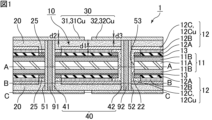
- FIG. 1 is a cross-sectional view illustrating an example of a capacitor element according to a first embodiment of the present invention.
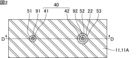
- FIG. 2 is a plan view taken along line AA of the capacitor element shown in FIG.
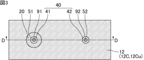
- FIG. 3 is a plan view of the capacitor element shown in FIG. 1 taken along line BB.
- FIG. 4 is a plan view of the capacitor element shown in FIG. 1 taken along line CC.
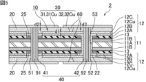
- FIG. 5 is a cross-sectional view illustrating a schematic diagram of another example of the capacitor element according to the first embodiment of the present invention.
- FIG. 6-1 is a schematic cross-sectional view illustrating an example of a method for manufacturing the capacitor element shown in FIG. 1, and shows a step of preparing an anode plate.
- FIG. 1 is a cross-sectional view illustrating an example of a method for manufacturing the capacitor element shown in FIG. 1, and shows a step of preparing an anode plate.
- FIG. 6-2 is a schematic cross-sectional view illustrating an example of a method for manufacturing the capacitor element shown in FIG. 1, and shows a step of forming a dielectric layer.
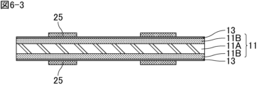
- FIG. 6-3 is a schematic cross-sectional view illustrating an example of a method for manufacturing the capacitor element shown in FIG. 1, showing a step of forming an insulating mask layer.
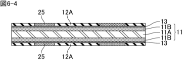
- FIG. 6-4 is a schematic cross-sectional view illustrating an example of a method for manufacturing the capacitor element shown in FIG. 1, and shows a step of forming a solid electrolyte layer.
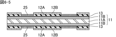
- FIG. 6-5 is a schematic cross-sectional view illustrating an example of a method for manufacturing the capacitor element shown in FIG. 1, and shows a step of forming a first conductive layer.
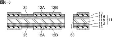
- 6-6 is a schematic cross-sectional view illustrating an example of a method for manufacturing the capacitor element shown in FIG. 1, showing a step of forming a through hole.
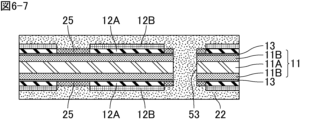
- 6 and 7 are schematic cross-sectional views illustrating an example of a method for manufacturing the capacitor element shown in FIG. 1, showing a step of forming an insulating material.
- 6 to 8 are schematic cross-sectional views illustrating an example of a method for manufacturing the capacitor element shown in FIG. 1, showing a step of polishing an insulating material.
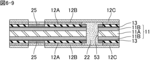
- 6-9 are schematic cross-sectional views illustrating an example of a method for manufacturing the capacitor element shown in FIG. 1, illustrating a step of forming a second conductive layer.
- 6 to 10 are schematic cross-sectional views illustrating an example of a method for manufacturing the capacitor element shown in FIG.
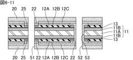
- FIG. 11 are schematic cross-sectional views illustrating an example of a method for manufacturing the capacitor element shown in FIG. 1, illustrating steps of forming the first through hole and the second through hole.
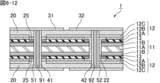
- 6 to 12 are schematic cross-sectional views illustrating an example of a method for manufacturing the capacitor element shown in FIG. 1, illustrating steps of forming through-hole conductors and external electrode layers.
- FIG. 7-1 is a schematic cross-sectional view illustrating another example of the method for manufacturing the capacitor element shown in FIG. 1, and shows a state after the through holes are formed.
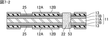
- FIG. 7-2 is a schematic cross-sectional view illustrating another example of the method for manufacturing the capacitor element shown in FIG. 1, illustrating a step of forming an insulating material.
- FIG. 7-1 is a schematic cross-sectional view illustrating another example of the method for manufacturing the capacitor element shown in FIG. 1, illustrating a step of forming an insulating material.
- FIG. 7-1 is a schematic cross-sectional view illustrating another example of the method for manufacturing the capacitor element
- FIG. 7-3 is a schematic cross-sectional view illustrating another example of the method for manufacturing the capacitor element shown in FIG. 1, illustrating the step of forming a second conductive layer.
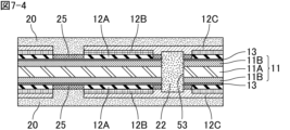
- FIG. 7-4 is a schematic cross-sectional view illustrating another example of the method for manufacturing the capacitor element shown in FIG. 1, illustrating a step of forming a sealing layer.
- FIG. 7-5 is a schematic cross-sectional view illustrating another example of the method for manufacturing the capacitor element shown in FIG. 1, illustrating a step of forming the first through hole and the second through hole.
- FIG. 7-6 is a schematic cross-sectional view illustrating another example of the method for manufacturing the capacitor element shown in FIG. 1, illustrating the steps of forming through-hole conductors and external electrode layers.
- FIG. 7-3 is a schematic cross-sectional view illustrating another example of the method for manufacturing the capacitor element shown in FIG. 1, illustrating the step of forming a second conductive layer.
- FIG. 7-4 is a schematic cross-sectional view illustrating another example
- FIG. 8 is a plan view illustrating an example of a capacitor element according to a second embodiment of the present invention.
- FIG. 9-1 is a schematic cross-sectional view illustrating an example of a method for manufacturing the capacitor element shown in FIG. 8, and shows a step of preparing an anode plate.
- FIG. 9-2 is a schematic cross-sectional view illustrating an example of a method for manufacturing the capacitor element shown in FIG. 8, and shows a step of forming a dielectric layer.
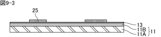
- FIG. 9-3 is a schematic cross-sectional view illustrating an example of a method for manufacturing the capacitor element shown in FIG. 8, and shows a step of forming an insulating mask layer.
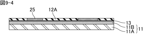
- FIG. 9-4 is a schematic cross-sectional view illustrating an example of a method for manufacturing the capacitor element shown in FIG.
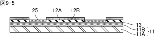
- FIG. 9-5 is a schematic cross-sectional view illustrating an example of a method for manufacturing the capacitor element shown in FIG. 8, and shows a step of forming a first conductive layer.
- FIG. 9-6 is a schematic cross-sectional view illustrating an example of a method for manufacturing the capacitor element shown in FIG. 8, showing a step of forming a through hole.
- FIG. 9-7 is a schematic cross-sectional view illustrating an example of a method for manufacturing the capacitor element shown in FIG. 8, and shows a step of forming an insulating material.
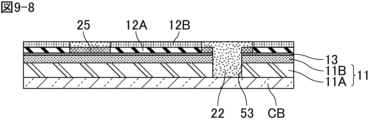
- FIG. 9-8 is a schematic cross-sectional view illustrating an example of a method for manufacturing the capacitor element shown in FIG.
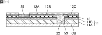
- FIG. 9-9 is a schematic cross-sectional view illustrating an example of a method for manufacturing the capacitor element shown in FIG. 8, and shows a step of forming a second conductive layer.
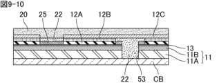
- 9 and 10 are schematic cross-sectional views illustrating an example of a method for manufacturing the capacitor element shown in FIG. 8, showing a step of forming a sealing layer.
- 9 to 11 are schematic cross-sectional views illustrating an example of a method for manufacturing the capacitor element shown in FIG. 8, illustrating steps of forming the first through hole and the second through hole.
- 9 to 12 are schematic cross-sectional views illustrating an example of a method for manufacturing the capacitor element shown in FIG. 8, showing steps of forming through-hole conductors and external electrode layers.
- the capacitor element of the present invention is described below. Note that the present invention is not limited to the following configuration, and may be modified as appropriate without changing the gist of the present invention. In addition, a combination of multiple individual preferred configurations described below also constitutes the present invention.
- each embodiment will simply be referred to as the "capacitor element of the present invention.”
- terms indicating the relationship between elements e.g., "perpendicular,” “parallel,” “orthogonal,” etc.
- terms indicating the shapes of elements are not expressions that express only a strict meaning, but are expressions that include a range of substantial equivalence, for example, differences of about a few percent.
- Fig. 1 is a cross-sectional view diagrammatically illustrating an example of a capacitor element according to a first embodiment of the present invention.
- Fig. 2 is a plan view taken along line A-A of the capacitor element shown in Fig. 1.
- Fig. 3 is a plan view taken along line B-B of the capacitor element shown in Fig. 1.
- Fig. 4 is a plan view taken along line CC of the capacitor element shown in Fig. 1.
- Fig. 1 is a cross-sectional view taken along line D-D of the capacitor element shown in Figs. 2 to 4.
- the capacitor element 1 shown in Figures 1 to 4 comprises a capacitor section 10, a sealing layer 20 provided to cover the capacitor section 10, a through-hole conductor 40 provided to penetrate the capacitor section 10 and the sealing layer 20 in the thickness direction and with both ends extended to the surface of the sealing layer 20, and an external electrode layer 30 provided on the surface of the sealing layer 20 so as to be electrically connected to the through-hole conductor 40.
- one capacitor section 10 is disposed inside the sealing layer 20.
- the number of capacitor sections 10 disposed inside the sealing layer 20 is not particularly limited, and may be one or more.
- the capacitor section 10 includes an anode plate 11 having a porous section 11B on at least one main surface of a core section 11A, a dielectric layer 13 provided on the surface of the porous section 11B, and a cathode layer 12 provided on the surface of the dielectric layer 13.
- the anode plate 11 has a porous section 11B on both main surfaces of the core section 11A, but it may have a porous section 11B on only one of the main surfaces of the core section 11A.
- the cathode layer 12 includes, for example, a solid electrolyte layer 12A provided on the surface of the dielectric layer 13.
- the capacitor section 10 constitutes a solid electrolytic capacitor.
- the sealing layer 20 is provided on both opposing main surfaces of the capacitor section 10 in the thickness direction.
- the capacitor section 10 is protected by the sealing layer 20.
- the sealing layer 20 may be composed of only one layer, or may be composed of two or more layers. When the sealing layer 20 is composed of two or more layers, the materials constituting each layer may be the same or different.
- the sealing layer 20 is formed to seal the capacitor section 10, for example, by a method of thermocompressing an insulating resin sheet, or by applying an insulating resin paste and then thermally curing it.
- the through-hole conductor 40 includes a first through-hole conductor 41 electrically connected to the anode plate 11 and a second through-hole conductor 42 electrically connected to the cathode layer 12.
- the first through-hole conductor 41 only needs to be provided on at least the inner wall surface of the first through hole 51 that penetrates the capacitor section 10 and the sealing layer 20 in the thickness direction.
- the first through-hole conductor 41 may be provided only on the inner wall surface of the first through hole 51, or may be provided throughout the entire interior of the first through hole 51.
- one first through-hole conductor 41 may be provided inside the cathode layer 12, or two or more first through-hole conductors 41 may be provided.
- the second through-hole conductor 42 may be provided at least on the inner wall surface of the second through hole 52 that penetrates the capacitor section 10 and the sealing layer 20 in the thickness direction.
- the second through-hole conductor 42 may be provided only on the inner wall surface of the second through hole 52, or may be provided throughout the entire interior of the second through hole 52.
- an insulating material 22 is filled between the second through-hole conductor 42 and the capacitor section 10 (particularly the anode plate 11).
- one second through-hole conductor 42 may be provided inside the cathode layer 12, or two or more second through-hole conductors 42 may be provided.
- the through-hole conductor 40 may include a third through-hole conductor that is not electrically connected to the anode plate 11 and the cathode layer 12.
- the external electrode layer 30 includes a first external electrode layer 31 electrically connected to the first through-hole conductor 41 and the anode plate 11, and a second external electrode layer 32 electrically connected to the second through-hole conductor 42 and the cathode layer 12.
- one first external electrode layer 31 may be provided, or multiple first external electrode layers 31 may be provided.
- one second external electrode layer 32 may be provided, or multiple second external electrode layers 32 may be provided.
- the number of first external electrode layers 31 may be the same as the number of second external electrode layers 32, or may be different.
- the planar shape of the external electrode layer 30 when viewed from the thickness direction is not particularly limited, and examples include a rectangle (square or oblong), a quadrangle other than a rectangle, a polygon such as a triangle, a pentagon, or a hexagon, a circle, an ellipse, or a shape that is a combination of these.
- the planar shape of the external electrode layer 30 may be an L-shape, a C-shape, a step shape, etc.
- the planar shape of the first external electrode layer 31 when viewed from the thickness direction may be the same as or different from the planar shape of the second external electrode layer 32 when viewed from the thickness direction.
- the cathode layer 12 may be drawn out by an internal via conductor as in the example shown in FIG. 5 described later, but in the example shown in FIG. 1, the second through-hole conductor 42 is electrically connected directly to the cathode layer 12, and the cathode layer 12 is drawn out by the second through-hole conductor 42. In this way, the second through-hole conductor 42 is electrically connected directly to the cathode layer 12, and the heat dissipation path, i.e., the heat dissipation area, can be increased compared to drawing out only by the internal via conductor.
- at least a portion of the first external electrode layer 31 overlaps the cathode layer 12 in the thickness direction, which also increases the heat dissipation area. As a result, the heat dissipation properties of the capacitor element 1 can be improved. As a result, the temperature rise due to heat generation in the capacitor element 1 can be suppressed.
- the second through-hole conductor 42 and the cathode layer 12 are in direct contact without going through a resin portion, which is a different material, and therefore the rigidity of the capacitor element 1 can be improved.
- the area of the first external electrode layer 31 can be increased, and therefore the rigidity of the capacitor element 1 can be improved.
- the capacitor element 1 can be made thinner, but there is a possibility that the capacitor element 1 may warp.
- the rigidity of the capacitor element 1 is improved and the occurrence of such warping can also be suppressed.
- the area of the first external electrode layer 31 can be increased, thereby preventing moisture, oxygen, etc. from entering the capacitor section 10 from the outside.
- a through-hole conductor when a through-hole conductor is electrically connected directly to a conductive layer such as a cathode layer or an anode plate, this excludes cases where the through-hole conductor only has a structure (connection path) that is electrically connected to the conductive layer via a via conductor or an external electrode layer.
- the through-hole conductor is electrically connected to the conductive layer on the inner wall surface of the through hole, that is, the side wall portion of the through-hole conductor is electrically connected to the conductive layer.
- the second through-hole conductor 42 is electrically connected to the cathode layer 12 on the inner wall surface of the second through hole 52.
- the first through-hole conductor 41 is also electrically connected directly to the anode plate 11, and the first through-hole conductor 41 is electrically connected to the anode plate 11 on the inner wall surface of the first through hole 51.
- the first external electrode layer 31 may only partially overlap the cathode layer 12 in the thickness direction.
- the ratio of the area of the portion overlapping the cathode layer 12 in the thickness direction to the total area of the first external electrode layer 31 is not particularly limited, but is preferably 50% or more and 90% or less, and more preferably 60% or more and 80% or less.
- the cathode layer 12 may include a copper layer 12Cu
- the first external electrode layer 31 may include a copper layer 31Cu
- the second external electrode layer 32 may include a copper layer 32Cu.
- the thickness of the copper layer 12Cu of the cathode layer 12 is d1
- the thickness of the copper layer 31Cu of the first external electrode layer 31 is d2
- the thickness of the copper layer 32Cu of the second external electrode layer 32 is d3
- heat diffusion can be promoted and damage to the capacitor section 10 can be suppressed.
- copper layer 12Cu is the second conductive layer 12C of the cathode layer 12 described below
- copper layer 31Cu is the first external electrode layer
- copper layer 32Cu is the second external electrode layer 32.
- the cathode layer 12 is composed of multiple layers including the copper layer 12Cu, it is preferable that the copper layer 12Cu is one or more layers that are closest to the first external electrode layer 31 and the second external electrode layer 32 among the multiple layers that compose the cathode layer 12.
- the copper layer 31Cu may be any one of the multiple layers that make up the cathode layer 12. The same applies to the second external electrode layer 32.
- the thickness of the core 11A of the anode plate 11 is, for example, 40 ⁇ m or more and 60 ⁇ m or less, and the area of the core 11A of the anode plate 11 is assumed to be approximately 100% in the plane along line A-A in Fig. 1 shown in Fig. 2.
- the thickness of the copper layer 12Cu of each cathode layer 12 is, for example, approximately 30 ⁇ m, and the area of the copper layer 12Cu is assumed to be approximately 100% in the plane along line B-B in Fig. 1 shown in Fig. 3.
- S1>S2 is the area of the first external electrode layer 31 electrically connected to the anode plate 11 and S2 is the area of the second external electrode layer 32 electrically connected to the cathode layer 12. Furthermore, by satisfying S1>S2, undulations (waviness) of the substrate on which the capacitor element 1 is mounted can also be suppressed.
- area means the area in a plan view from the thickness direction.
- the ratio of S1 to S2, i.e., S1/S2, preferably satisfies 1 ⁇ S1/S2 ⁇ 3.5, and more preferably satisfies 1.5 ⁇ S1/S2 ⁇ 3.
- Comparisons such as S1>S2 and S1/S2 are made based on the areas of the first external electrode layer 31 and the second external electrode layer 32 provided on the same main surface side of the capacitor section 10.
- the cathode layer 12 preferably includes a solid electrolyte layer 12A provided on the surface of the dielectric layer 13, a first conductor layer 12B provided on the surface of the solid electrolyte layer 12A, and a second conductor layer 12C provided on the surface of the first conductor layer 12B so as to be electrically connected directly to the second through-hole conductor 42. This allows the second through-hole conductor 42 to be easily electrically connected directly to the cathode layer 12.
- the areas of the first through-hole conductors 41 and the second through-hole conductors 42 provided in the capacitor element 1 are the same, and it is even more preferable that the numbers of the first through-hole conductors 41 and the second through-hole conductors 42 provided in the capacitor element 1 are the same. This makes it possible to make the heat dissipation properties of the capacitor element 1 uniform.
- the through-hole conductors 40 i.e., the first through-hole conductor 41 and the second through-hole conductor 42 are not distinguished from each other
- the through-hole conductors 40 are arranged at an equal pitch. This also makes it possible to make the heat dissipation properties of the capacitor element 1 uniform. It is also possible to suppress the occurrence of peeling called delamination, such as peeling of the cathode layer from the anode plate.
- the capacitor section 10 further includes an insulating mask layer 25 provided around the through-hole conductor 40 on at least one of the main surfaces of the anode plate 11.
- an insulating mask layer 25 is provided between the first through-hole conductor 41 and the cathode layer 12. Also, in the example shown in FIG. 1, an insulating material 22 is filled between the second through-hole conductor 42 and the capacitor section 10 (particularly the anode plate 11), and an insulating mask layer 25 is provided between this insulating material 22 and the cathode layer 12 (e.g., the solid electrolyte layer 12A).
- the capacitor section 10 may further include an insulating mask layer 25 provided on at least one main surface of the anode plate 11 so as to surround the periphery of the cathode layer 12 (e.g., solid electrolyte layer 12A; the same applies hereinafter in this paragraph).
- an insulating mask layer 25 provided on at least one main surface of the anode plate 11 so as to surround the periphery of the cathode layer 12 (e.g., solid electrolyte layer 12A; the same applies hereinafter in this paragraph).
- the insulating mask layer 25 may be provided so as to surround a portion of the periphery of the cathode layer 12, but it is preferable that the insulating mask layer 25 be provided so as to surround the entire periphery of the cathode layer 12.
- FIG. 5 is a cross-sectional view showing a schematic diagram of another example of a capacitor element according to the first embodiment of the present invention.
- the capacitor element 2 shown in FIG. 5 further includes an internal via conductor 60 that is arranged to penetrate the sealing layer 20 in the thickness direction, with one end electrically connected to the second external electrode layer 32 and the other end electrically connected to the cathode layer 12.
- an internal via conductor 60 By providing such an internal via conductor 60, it is possible to further improve heat dissipation. It is also possible to improve adhesion between layers and suppress the occurrence of delamination.
- one end of the internal via conductor 60 is extended to the surface of the sealing layer 20.
- the internal via conductor 60 is also electrically connected to the cathode layer 12. This allows the cathode layer 12 to be electrically led out to the outside of the sealing layer 20 via the internal via conductor 60 and the second through-hole conductor 42, and to be electrically connected to the outside of the sealing layer 20. There may be one internal via conductor 60 electrically connected to the cathode layer 12, or two or more internal via conductors 60.
- the capacitor element 2 may include an internal via conductor 60 electrically connected to the anode plate 11.
- the anode plate 11 is electrically led out to the outside of the sealing layer 20 via the internal via conductor 60, and can be electrically connected to the outside of the sealing layer 20.
- capacitor elements 1, 2, etc. The detailed configuration of capacitor elements 1, 2, etc. is explained below.
- the planar shape of the capacitor section 10 when viewed from the thickness direction may be, for example, a rectangle (square or oblong), a quadrangle other than a rectangle, a polygon such as a triangle, a pentagon, or a hexagon, a circle, an ellipse, or a combination of these.
- the planar shape of the capacitor section 10 may also be an L-shape, a C-shape, a stepped shape, or the like.
- the anode plate 11 is preferably made of a valve metal that exhibits so-called valve action.
- valve metals include simple metals such as aluminum, tantalum, niobium, titanium, and zirconium, or alloys containing at least one of these metals. Of these, aluminum or an aluminum alloy is preferred.
- the shape of the anode plate 11 is preferably flat, and more preferably foil-like.
- plate-like includes “foil-like”.
- the anode plate 11 may have a porous portion 11B on at least one main surface of the core portion 11A.
- the anode plate 11 may have a porous portion 11B on only one main surface of the core portion 11A as in the second embodiment described below, or may have a porous portion 11B on both main surfaces of the core portion 11A.
- the porous portion 11B is preferably a porous layer formed on the surface of the core portion 11A, and is more preferably an etched layer.
- the thickness of the anode plate 11 before the etching process is preferably 60 ⁇ m or more and 200 ⁇ m or less.
- the thickness of the unetched core portion 11A after the etching process is preferably 15 ⁇ m or more and 70 ⁇ m or less.
- the thickness of the porous portion 11B is designed according to the required withstand voltage and electrostatic capacitance, but it is preferable that the combined thickness of the porous portions 11B on both sides of the core portion 11A is 10 ⁇ m or more and 180 ⁇ m or less.
- the pore diameter of the porous portion 11B is preferably 10 nm or more and 600 nm or less.
- the pore diameter of the porous portion 11B means the median diameter D50 measured by a mercury porosimeter.
- the pore diameter of the porous portion 11B can be controlled, for example, by adjusting various etching conditions.
- the dielectric layer 13 provided on the surface of the porous portion 11B is porous, reflecting the surface condition of the porous portion 11B, and has a finely uneven surface shape.
- the dielectric layer 13 is preferably made of an oxide film of the valve metal.
- the dielectric layer 13 made of an oxide film can be formed by anodizing the surface of the aluminum foil in an aqueous solution containing ammonium adipate or the like (also called chemical conversion treatment).
- the thickness of the dielectric layer 13 is designed according to the required withstand voltage and capacitance, but is preferably 10 nm or more and 100 nm or less.
- the cathode layer 12 includes a solid electrolyte layer 12A
- examples of materials constituting the solid electrolyte layer 12A include conductive polymers such as polypyrroles, polythiophenes, and polyanilines. Among these, polythiophenes are preferred, and poly(3,4-ethylenedioxythiophene), also known as PEDOT, is particularly preferred.
- the conductive polymer may also include a dopant such as polystyrene sulfonate (PSS).
- PSS polystyrene sulfonate
- the solid electrolyte layer 12A preferably includes an inner layer that fills the pores (recesses) of the dielectric layer 13, and an outer layer that covers the dielectric layer 13.
- the thickness of the solid electrolyte layer 12A from the surface of the porous portion 11B is preferably 2 ⁇ m or more and 20 ⁇ m or less.
- the solid electrolyte layer 12A is formed, for example, by a method of forming a polymerized film of poly(3,4-ethylenedioxythiophene) or the like on the surface of the dielectric layer 13 using a treatment liquid containing a monomer such as 3,4-ethylenedioxythiophene, or by applying a dispersion of a polymer such as poly(3,4-ethylenedioxythiophene) to the surface of the dielectric layer 13 and drying it.
- the solid electrolyte layer 12A can be formed in a predetermined area by applying the above-mentioned treatment liquid or dispersion liquid to the surface of the dielectric layer 13 by a method such as sponge transfer, screen printing, dispenser application, or inkjet printing.
- the first conductive layer 12B and the second conductive layer 12C each include at least one of a conductive resin layer and a metal layer.
- the first conductive layer 12B and the second conductive layer 12C may each be only a conductive resin layer or only a metal layer, but it is preferable that the first conductive layer 12B is composed only of a conductive resin layer, and the second conductive layer 12C is preferably composed only of a metal layer.
- the first conductive layer 12B preferably covers the entire surface of the solid electrolyte layer 12A.
- the conductive resin layer may be, for example, a conductive adhesive layer (conductive paste layer) containing at least one conductive filler selected from the group consisting of silver filler, copper filler, nickel filler, and carbon filler.
- a conductive adhesive layer conductive paste layer
- conductive filler selected from the group consisting of silver filler, copper filler, nickel filler, and carbon filler.
- the metal layer examples include a metal plating layer and a metal foil layer.
- the metal layer is preferably made of at least one metal selected from the group consisting of nickel, copper, silver, and alloys containing these metals as main components.
- the term "main component" refers to the elemental component with the largest weight ratio.
- the first conductive layer 12B includes, for example, a carbon paste layer provided on the surface of the solid electrolyte layer 12A and a copper paste layer provided on the surface of the carbon paste layer.
- the second conductive layer 12C is composed of a copper layer 12Cu, such as a copper plating layer or a copper foil layer.
- the thickness d1 of the copper layer 12Cu of the cathode layer 12 described above is the combined thickness of the copper layer 12Cu of the second conductor layer 12C and the copper paste layer of the first conductor layer 12B.
- the carbon paste layer of the first conductor layer 12B is provided to electrically and mechanically connect the solid electrolyte layer 12A and the copper paste layer of the first conductor layer 12B.
- the carbon paste layer can be formed in a predetermined area by applying carbon paste to the surface of the solid electrolyte layer 12A by sponge transfer, screen printing, dispenser application, inkjet printing, or other methods. It is preferable to laminate the copper paste layer in the next process to the carbon paste layer while it is still viscous before drying.
- the thickness of the carbon paste layer is preferably 2 ⁇ m or more and 50 ⁇ m or less.
- the copper paste layer of the first conductive layer 12B can be formed in a predetermined area by applying copper paste to the surface of the carbon paste layer by sponge transfer, screen printing, spray application, dispenser application, inkjet printing, or other methods.
- the thickness of the copper paste layer is preferably 2 ⁇ m or more and 50 ⁇ m or less.
- the copper plating layer of the second conductive layer 12C can be formed in a predetermined area by forming a film by electrolytic plating, electroless plating, sputtering, vacuum deposition, etc., and then patterning it by etching (dry or wet).
- the thickness of the copper plating layer is preferably 2 ⁇ m or more and 35 ⁇ m or less.
- the copper foil layer of the second conductive layer 12C can be formed in a predetermined area by laminating copper foil that has previously been patterned by etching (dry or wet) in a press, or by laminating copper foil in a press and then patterning it by etching (dry or wet).
- the thickness of the copper foil layer is preferably 3 ⁇ m or more and 35 ⁇ m or less.
- the sealing layer 20 is made of an insulating material. In this case, it is preferable that the sealing layer 20 is made of an insulating resin.
- Examples of the insulating resin that constitutes the sealing layer 20 include epoxy resin, phenolic resin, etc.
- the sealing layer 20 further contains a filler.
- the filler contained in the sealing layer 20 may be, for example, an inorganic filler such as silica particles or alumina particles.
- a layer such as a stress relief layer or a moisture-proof film may be provided.
- the insulating mask layer 25 is made of an insulating material. In this case, it is preferable that the insulating mask layer 25 is made of an insulating resin.
- Examples of insulating resins constituting the insulating mask layer 25 include polyphenylsulfone resin, polyethersulfone resin, cyanate ester resin, fluororesin (tetrafluoroethylene, tetrafluoroethylene-perfluoroalkylvinylether copolymer, etc.), polyimide resin, polyamideimide resin, epoxy resin, and derivatives or precursors thereof.
- the insulating mask layer 25 may be made of the same resin as the sealing layer 20. Unlike the sealing layer 20, if the insulating mask layer 25 contains inorganic filler, this may adversely affect the effective capacitance portion of the capacitor section 10, so it is preferable that the insulating mask layer 25 is made of a resin alone.
- the insulating mask layer 25 can be formed in a predetermined area by applying a mask material, such as a composition containing an insulating resin, to the surface of the porous portion 11B by a method such as sponge transfer, screen printing, dispenser application, or inkjet printing.
- a mask material such as a composition containing an insulating resin
- the insulating mask layer 25 may be formed on the porous portion 11B either before the dielectric layer 13 or after the dielectric layer 13.
- the first external electrode layer 31 is electrically connected to the anode plate 11.
- the first external electrode layer 31 is provided on the surface of the first through-hole conductor 41, and functions as a connection terminal for the capacitor section 10.
- the first external electrode layer 31 is electrically connected to the anode plate 11 via the first through-hole conductor 41, and functions as a connection terminal for the anode plate 11.
- the constituent material of the first external electrode layer 31 may be, for example, a metal material containing a low-resistance metal such as silver, gold, or copper.
- the first external electrode layer 31 is formed, for example, by plating the surface of the first through-hole conductor 41.
- a mixed material (conductive paste material) of at least one conductive filler selected from the group consisting of silver filler, copper filler, nickel filler, and carbon filler and resin may be used as the constituent material of the first external electrode layer 31.
- the first external electrode layer 31 may include a copper layer 31Cu such as a copper paste layer, a copper plating layer, a copper foil layer, etc.
- the copper paste layer, copper plating layer, and copper foil layer of the first external electrode layer 31 can be formed in the same manner as the copper paste layer of the first conductive layer 12B, and the copper plating layer and copper foil layer of the second conductive layer 12C.
- the second external electrode layer 32 is electrically connected to the cathode layer 12.
- the second external electrode layer 32 is provided on the surface of the second through-hole conductor 42, and functions as a connection terminal for the capacitor section 10.
- the second external electrode layer 32 is electrically connected to the cathode layer 12 via the second through-hole conductor 42, and functions as a connection terminal for the cathode layer 12.
- the second external electrode layer 32 may be made of a metal material containing a low-resistance metal such as silver, gold, or copper.
- the second external electrode layer 32 is formed by, for example, plating the surface of the second through-hole conductor 42.
- a mixed material (conductive paste material) of at least one conductive filler selected from the group consisting of silver filler, copper filler, nickel filler, and carbon filler and resin may be used as the constituent material of the second external electrode layer 32.
- the second external electrode layer 32 may include a copper layer 32Cu, such as a copper paste layer, a copper plating layer, a copper foil layer, etc.
- the copper paste layer, copper plating layer, and copper foil layer of the second external electrode layer 32 can be formed in the same manner as the copper paste layer of the first conductive layer 12B, and the copper plating layer and copper foil layer of the second conductive layer 12C.
- the constituent materials of the first external electrode layer 31 and the second external electrode layer 32 are preferably the same as each other at least in terms of type, but may be different from each other.
- each of the multiple capacitor sections 10 may be provided with a first external electrode layer 31 electrically connected to the anode plate 11 and a second external electrode layer 32 electrically connected to the cathode layer 12, or at least one of the first external electrode layer 31 and the second external electrode layer 32 may be provided in common among the multiple capacitor sections 10.
- the first external electrode layer 31 and the second external electrode layer 32 are provided on both main surfaces of the sealing layer 20, but they may be provided on only one main surface of the sealing layer 20.
- the first through-hole conductor 41 is electrically connected to the anode plate 11 on the inner wall surface of the first through hole 51. More specifically, it is preferable that the first through-hole conductor 41 is electrically connected to the end surface of the anode plate 11 that faces the inner wall surface of the first through hole 51 in the planar direction. As a result, the anode plate 11 is electrically led out to the outside via the first through-hole conductor 41.
- the core portion 11A and the porous portion 11B are exposed on the end face of the anode plate 11 that is electrically connected to the first through-hole conductor 41.
- the porous portion 11B as well as the core portion 11A are electrically connected to the first through-hole conductor 41.
- the first through-hole conductor 41 is electrically connected to the anode plate 11 around the entire circumference of the first through hole 51.
- the number of paths for heat dissipation is increased, and the heat dissipation performance of the capacitor element 1 can be further improved.
- the connection resistance between the anode plate 11 and the first through-hole conductor 41 is likely to decrease, and therefore the equivalent series resistance (ESR) is likely to decrease.
- the first through-hole conductor 41 is formed, for example, as follows. First, a first through hole 51 penetrating the capacitor section 10 and the sealing layer 20 in the thickness direction is formed by drilling, laser processing, or the like. Then, the inner wall surface of the first through hole 51 is metallized with a metal material containing a low-resistance metal such as copper, gold, or silver to form the first through-hole conductor 41. When forming the first through-hole conductor 41, for example, the inner wall surface of the first through hole 51 is metallized with an electroless copper plating process, an electrolytic copper plating process, or the like to facilitate processing.
- the method of forming the first through-hole conductor 41 may be a method of filling the first through hole 51 with a metal material, a composite material of metal and resin, or the like, in addition to a method of metallizing the inner wall surface of the first through hole 51.
- An anode connection layer may be provided between the anode plate 11 and the first through-hole conductor 41 in the surface direction.
- the anode plate 11 and the first through-hole conductor 41 may be electrically connected via the anode connection layer.
- the anode connection layer is provided between the anode plate 11 and the first through-hole conductor 41 in the surface direction, so that the anode connection layer functions as a barrier layer for the anode plate 11, more specifically, as a barrier layer for the core portion 11A and the porous portion 11B.
- the anode connection layer functions as a barrier layer for the anode plate 11
- dissolution of the anode plate 11 that occurs during chemical treatment to form the external electrode layer 30 e.g., the first external electrode layer 31
- the infiltration of the chemical solution into the capacitor portion 10 is suppressed, which tends to improve reliability.
- the anode connection layer preferably includes a layer mainly composed of nickel. In this case, damage to the metal (e.g., aluminum) constituting the anode plate 11 is reduced, and the barrier properties of the anode connection layer against the anode plate 11 are easily improved.
- the metal e.g., aluminum
- an anode connection layer does not have to be provided between the anode plate 11 and the first through-hole conductor 41 in the surface direction.
- the first through-hole conductor 41 may be directly connected to the end surface of the anode plate 11.
- the first through-hole conductor 41 is provided only on the inner wall surface of the first through hole 51.
- the first through hole 51 may be provided with a resin filling portion 91 filled with a resin material.
- the resin filling portion 91 is provided in the space surrounded by the first through-hole conductor 41 in the first through hole 51.
- the resin filling portion 91 may be a conductor or an insulator.
- the second through-hole conductor 42 is electrically connected to the cathode layer 12, particularly to the second conductive layer 12C, on the inner wall surface of the second through hole 52. More specifically, it is preferable that the second through-hole conductor 42 is electrically connected to the end surface of the second conductive layer 12C that faces the inner wall surface of the second through hole 52 in the planar direction. As a result, the cathode layer 12 is electrically led out to the outside via the second through-hole conductor 42.
- the second through-hole conductor 42 is electrically connected to the cathode layer 12, particularly the second conductive layer 12C, around the entire circumference of the second through hole 52.
- the number of paths for heat dissipation is increased, and the heat dissipation properties of the capacitor element 1 can be further improved.
- the connection resistance between the cathode layer 12 and the second through-hole conductor 42 is likely to decrease, and therefore the equivalent series resistance (ESR) is likely to decrease.
- the second through-hole conductor 42 is formed, for example, as follows. First, a through hole 53 penetrating the capacitor section 10 in the thickness direction is formed by drilling, laser processing, etc. Next, the above-mentioned through hole 53 is filled with the insulating material 22. The part filled with the insulating material 22 is drilled, laser processing, etc. to form the second through hole 52. At this time, the diameter of the second through hole 52 is made smaller than the diameter of the through hole 53 filled with the insulating material 22, so that the insulating material 22 is present between the inner wall surface of the previously formed through hole 53 and the inner wall surface of the second through hole 52 in the surface direction.
- the inner wall surface of the second through hole 52 is metallized with a metal material containing a low-resistance metal such as copper, gold, or silver, to form the second through-hole conductor 42.
- a metal material containing a low-resistance metal such as copper, gold, or silver
- the inner wall surface of the second through hole 52 is metallized with electroless copper plating, electrolytic copper plating, etc., to facilitate processing.
- the method of forming the second through-hole conductor 42 may be a method of filling the second through-hole 52 with a metal material, a composite material of metal and resin, or the like, in addition to a method of metallizing the inner wall surface of the second through-hole 52.
- the insulating material 22 is preferably composed of an insulating resin.
- the insulating resin that constitutes the insulating material 22 include epoxy resin and phenol resin.
- the insulating material 22 preferably contains a filler.
- the filler contained in the insulating material 22 include inorganic fillers such as silica particles, alumina particles, and metal particles.
- the insulating material 22 may be made of the same material as the sealing layer 20.
- a cathode connection layer such as an anode connection layer may be provided between the cathode layer 12, particularly the second conductive layer 12C, and the second through-hole conductor 42, but it is preferable that no cathode connection layer is provided.
- the second through-hole conductor 42 may be directly connected to the end face of the second conductive layer 12C.
- the second through-hole conductor 42 is provided only on the inner wall surface of the second through hole 52.
- the second through hole 52 may be provided with a resin filling portion 92 filled with a resin material.
- the resin filling portion 92 is provided in the space surrounded by the second through-hole conductor 42 in the second through hole 52.
- the resin filling portion 92 may be a conductor or an insulator.
- Examples of materials that can be used to form the internal via conductor 60 include metal materials that contain low-resistance metals such as silver, gold, and copper.
- the internal via conductor 60 is formed, for example, by plating the inner wall surface of a through hole that penetrates the sealing layer 20 in the thickness direction with the metal material described above, or by filling it with a conductive paste and then performing a heat treatment.
- FIGS. 6-1 to 6-12 are schematic cross-sectional views illustrating an example of a method for manufacturing the capacitor element shown in FIG. 1.
- FIG. 6-1 shows the process of preparing an anode plate.
- FIG. 6-2 shows the process of forming a dielectric layer.
- FIG. 6-3 shows the process of forming an insulating mask layer.
- FIG. 6-4 shows the process of forming a solid electrolyte layer.
- FIG. 6-5 shows the process of forming a first conductive layer.
- FIG. 6-6 shows the process of forming a through hole.
- FIG. 6-7 shows the process of forming an insulating material.
- FIG. 6-8 shows the process of polishing the insulating material.
- FIG. 6-9 shows the process of forming a second conductive layer.
- FIG. 6-10 shows the process of forming a sealing layer.
- FIG. 6-11 shows the process of forming a first through hole and a second through hole.
- FIG. 6-12 shows the process of forming
- the capacitor element 1 shown in FIG. 1 is formed, for example, as follows.
- a dielectric layer 13 is formed on the porous portion 11B.
- an insulating mask layer 25 is formed on the dielectric layer 13.
- a solid electrolyte layer 12A is formed on the dielectric layer 13 in the area surrounded by the insulating mask layer 25.
- a first conductive layer 12B is formed on the solid electrolyte layer 12A.
- a through hole 53 is formed through the insulating mask layer 25, the dielectric layer 13, and the anode plate 11.
- an insulating material 22 is laminated to cover the insulating mask layer 25 and the first conductive layer 12B, and the through holes 53 are filled with the insulating material 22.
- the insulating material 22 is polished to thin it until the first conductive layer 12B is exposed.
- a second conductive layer 12C is formed on the first conductive layer 12B and the insulating material 22.
- a sealing layer 20 is formed to cover the second conductive layer 12C and the insulating material 22.
- a first through hole 51 is formed that penetrates the sealing layer 20, the insulating material 22, the insulating mask layer 25, the dielectric layer 13, and the anode plate 11, and a second through hole 52 is formed that penetrates the sealing layer 20, the second conductive layer 12C, and the insulating material 22.
- the second through hole 52 is located inside the area where the through hole 53 was formed.
- a first through-hole conductor 41 is formed in the first through-hole 51, and a second through-hole conductor 42 is formed in the second through-hole 52. Resin filling portions 91 and 92 may be formed in the first through-hole conductor 41 and the second through-hole conductor 42, respectively.
- a first external electrode layer 31 is formed on the sealing layer 20 so as to cover the first through-hole conductor 41, and a second external electrode layer 32 is formed on the sealing layer 20 so as to cover the second through-hole conductor 42.
- FIGS. 7-1 to 7-6 are schematic cross-sectional views illustrating another example of a method for manufacturing the capacitor element shown in FIG. 1.
- FIG. 7-1 shows the state after the through holes have been formed.
- FIG. 7-2 shows the step of forming an insulating material.
- FIG. 7-3 shows the step of forming a second conductive layer.
- FIG. 7-4 shows the step of forming a sealing layer.
- FIG. 7-5 shows the step of forming a first through hole and a second through hole.
- FIG. 7-6 shows the step of forming a through-hole conductor and an external electrode layer.
- the capacitor element 1 shown in FIG. 1 may be formed, for example, as follows.
- a through hole 53 is formed through the insulating mask layer 25, the dielectric layer 13, and the anode plate 11 in the same manner as shown in FIG. 6-1 to FIG. 6-6.
- insulating material 22 is formed only inside through-hole 53 by filling with resin material, screen printing, dispenser application, inkjet printing, or the like.
- the second conductive layer 12C, the sealing layer 20, the first through hole 51, the second through hole 52, the first through-hole conductor 41, the second through-hole conductor 42, the first external electrode layer 31, and the second external electrode layer 32 are formed.
- resin filling portions 91 and 92 may be formed as necessary.
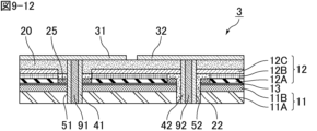
- FIG. 8 is a plan view illustrating an example of a capacitor element according to a second embodiment of the present invention.
- the anode plate 11 has a porous portion 11B on only one main surface of the core portion 11A, and each component such as the capacitor portion 10 (anode plate 11, dielectric layer 13, and cathode layer 12), sealing layer 20, and external electrode layer 30 (first external electrode layer 31 and second external electrode layer 32) is provided on only one side of the capacitor element 3.
- one end of the through-hole conductors 40 (first through-hole conductor 41 and second through-hole conductor 42) is electrically connected to the external electrode layer 30, but the other end is exposed to the surface on which the capacitor section 10, etc. are not provided.
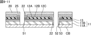
- FIG. 9-1 to FIG. 9-12 are schematic cross-sectional views illustrating an example of a method for manufacturing the capacitor element shown in FIG. 8.
- FIG. 9-1 shows the process of preparing an anode plate.
- FIG. 9-2 shows the process of forming a dielectric layer.
- FIG. 9-3 shows the process of forming an insulating mask layer.
- FIG. 9-4 shows the process of forming a solid electrolyte layer.
- FIG. 9-5 shows the process of forming a first conductive layer.
- FIG. 9-6 shows the process of forming a through hole.
- FIG. 9-7 shows the process of forming an insulating material.
- FIG. 9-8 shows the process of polishing the insulating material.
- FIG. 9-9 shows the process of forming a second conductive layer.
- FIG. 9-10 shows the process of forming a sealing layer.
- FIG. 9-11 shows the process of forming a first through hole and a second through hole.
- FIG. 9-12 shows the process of forming
- the capacitor element 3 shown in FIG. 8 may be formed, for example, as follows.
- the dielectric layer 13, the insulating mask layer 25, the solid electrolyte layer 12A, and the first conductive layer 12B are formed in the same manner as shown in Figures 6-2 to 6-5.
- the capacitor element sheet with the through holes 53 formed therein is placed on the carrier board CB in the same manner as shown in FIG. 6-6.
- the insulating material 22 is laminated and polished, and then the second conductive layer 12C, the sealing layer 20, the first through hole 51, the second through hole 52, the first through-hole conductor 41, the second through-hole conductor 42, the first external electrode layer 31, and the second external electrode layer 32 are formed.
- resin filling portions 91 and 92 may be formed as necessary.
- the capacitor element of the present invention is not limited to the above-described embodiment, and various applications and modifications can be made within the scope of the present invention with respect to the configuration, manufacturing conditions, and the like of the capacitor element.
- one capacitor section may be disposed inside the sealing layer, or multiple capacitor sections may be disposed inside the sealing layer.
- adjacent capacitor parts when multiple capacitor parts are arranged inside the sealing layer, adjacent capacitor parts only need to be physically separated from each other. Therefore, adjacent capacitor parts may be electrically separated from each other or electrically connected to each other. It is preferable that the part where adjacent capacitor parts are separated from each other is filled with an insulating material such as a sealing layer. The distance between adjacent capacitor parts may be constant in the thickness direction or may become smaller in the thickness direction.
- the multiple capacitor parts when multiple capacitor parts are arranged inside the sealing layer, the multiple capacitor parts may be arranged so as to be lined up in the planar direction, or so as to be stacked in the thickness direction, or a combination of both.
- the multiple capacitor parts may be arranged regularly or irregularly.
- the size and shape, etc. of the capacitor elements may be the same, or may be partially or entirely different. It is preferable that the configuration of each capacitor element is the same, but capacitor elements with different configurations may be included.
- the capacitor element of the present invention can be suitably used as a constituent material of a composite electronic component.
- a composite electronic component includes, for example, the capacitor element of the present invention, an external electrode layer provided on the surface of the sealing layer of the capacitor element and electrically connected to each of the anode plate and cathode layer of the capacitor element, and an electronic component connected to the external electrode layer.
- the electronic component connected to the external electrode layer may be a passive element or an active element. Both the passive element and the active element may be connected to the external electrode layer, or either the passive element or the active element may be connected to the external electrode layer. Also, a composite of a passive element and an active element may be connected to the external electrode layer.
- Passive elements include, for example, inductors. Active elements include memory, GPUs (Graphical Processing Units), CPUs (Central Processing Units), MPUs (Micro Processing Units), PMICs (Power Management ICs), etc.
- the capacitor element of the present invention has a sheet-like shape overall. Therefore, in a composite electronic component, the capacitor element can be treated like a mounting board, and electronic components can be mounted on the capacitor element. Furthermore, by making the electronic components to be mounted on the capacitor element into a sheet-like shape, it is also possible to connect the capacitor element and the electronic components in the thickness direction via through-hole conductors that penetrate each electronic component in the thickness direction. As a result, the active elements and passive elements can be configured like a single module.
- a switching regulator can be formed by electrically connecting the capacitor element of the present invention between a voltage regulator including a semiconductor active element and a load to which the converted DC voltage is supplied.
- a circuit layer may be formed on one side of a capacitor matrix sheet on which a plurality of capacitor elements of the present invention are laid out, and the capacitor elements may then be connected to passive or active elements.
- the capacitor element of the present invention may be placed in a cavity portion previously provided in a substrate, embedded in resin, and then a circuit layer may be formed on the resin.
- Another electronic component passive element or active element
- the capacitor element of the present invention may be mounted on a smooth carrier such as a wafer or glass, an outer layer made of resin may be formed, a circuit layer may be formed, and then the capacitor element may be connected to a passive or active element.
- a capacitor section including an anode plate having a porous portion on at least one main surface of a core portion, a dielectric layer provided on a surface of the porous portion, and a cathode layer provided on a surface of the dielectric layer; a sealing layer provided to cover the capacitor portion; a first through-hole conductor provided to penetrate the capacitor portion and the sealing layer in a thickness direction so as to be electrically connected directly to the anode plate, the first through-hole conductor having both ends extending to the surface of the sealing layer; a second through-hole conductor provided to penetrate the capacitor portion and the sealing layer in the thickness direction so as to be electrically connected directly to the cathode layer, the second through-hole conductor having both ends extending to the surface of the sealing layer; a first external electrode layer provided on a surface of the sealing layer so as to be electrically connected to the first through-hole conductor; a second external electrode layer provided on a surface of the sealing layer so as to be electrically connected to the second through-hole conductor
- the cathode layer, the first external electrode layer, and the second external electrode layer each include a copper layer;
- the thickness of the copper layer of the cathode layer is d1
- the thickness of the copper layer of the first external electrode layer is d2
- the thickness of the copper layer of the second external electrode layer is d3
- ⁇ 4> The capacitor element described in any one of ⁇ 1> to ⁇ 3> further comprising an internal via conductor that is provided so as to penetrate the sealing layer in the thickness direction, one end of which is electrically connected to the second external electrode layer and the other end of which is electrically connected to the cathode layer.
- the cathode layer includes: a solid electrolyte layer provided on a surface of the dielectric layer; a first conductor layer provided on the surface of the solid electrolyte layer; and a second conductor layer provided on the surface of the first conductor layer so as to be directly electrically connected to the second through-hole conductor.
Landscapes
- Engineering & Computer Science (AREA)
- Power Engineering (AREA)
- Microelectronics & Electronic Packaging (AREA)
- Fixed Capacitors And Capacitor Manufacturing Machines (AREA)
Abstract
コンデンサ素子1は、芯部11Aの少なくとも一方の主面に多孔質部11Bを有する陽極板11と、多孔質部11Bの表面に設けられた誘電体層13と、誘電体層13の表面に設けられた陰極層12と、を含むコンデンサ部10と、コンデンサ部10を覆うように設けられた封止層20と、陽極板11に電気的に直接接続されるようにコンデンサ部10及び封止層20を厚さ方向に貫通するように設けられ、両方の端部が封止層20の表面に引き出された第1スルーホール導体41と、陰極層12に電気的に直接接続されるようにコンデンサ部10及び封止層20を厚さ方向に貫通するように設けられ、両方の端部が封止層20の表面に引き出された第2スルーホール導体42と、第1スルーホール導体41に電気的に接続されるように封止層20の表面に設けられた第1外部電極層31と、第2スルーホール導体42に電気的に接続されるように封止層20の表面に設けられた第2外部電極層32と、を備え、第1外部電極層31の少なくとも一部は、厚さ方向において陰極層12に重なる。
Description
本発明は、コンデンサ素子に関する。
特許文献1には、少なくとも片面に多孔質部が設けられ所定の位置に貫通孔が形成された箔状の陽極と、上記陽極の多孔質部に形成された誘電体被膜と、上記誘電体被膜に形成された開口部を有する絶縁層と、上記絶縁層の開口部の上記誘電体被膜に形成された固体電解質層と、上記固体電解質層の少なくとも一部に形成され、上記陽極と略平行に配置された陰極と、上記絶縁層に形成された電極と、上記絶縁層及び上記陽極を貫通し、上記電極-上記陽極間を電気接続する及び/又は、上記絶縁層及び上記陰極を貫通し、上記電極-上記陰極間を電気接続するスルーホール電極を備え、上記スルーホール電極の少なくとも一つが、長孔形状である固体電解コンデンサが記載されている。
近年、電子機器の小型化及び高出力化に伴い、部品の高密度化が求められている。そのため、コンデンサ素子を電源直下の基板、例えばGPU(Graphical Processing Unit)基板等に埋め込むことが検討されている。当該用途では大電流が流されるが、従来のコンデンサ素子の構造では放熱性が不充分であり、コンデンサ素子の内部抵抗により熱が発生する可能性がある。このような各種部品からの発熱は、電子機器の安全性、信頼性、性能、寿命等に悪影響を及ぼす可能性がある。
特許文献1に記載の固体電解コンデンサについても、放熱性を向上するという点で改善の余地があった。
本発明は、上記の問題を解決するためになされたものであり、放熱性を向上することが可能なコンデンサ素子を提供することを目的とする。
本発明のコンデンサ素子は、芯部の少なくとも一方の主面に多孔質部を有する陽極板と、上記多孔質部の表面に設けられた誘電体層と、上記誘電体層の表面に設けられた陰極層と、を含むコンデンサ部と、上記コンデンサ部を覆うように設けられた封止層と、上記陽極板に電気的に直接接続されるように上記コンデンサ部及び上記封止層を厚さ方向に貫通するように設けられ、両方の端部が上記封止層の表面に引き出された第1スルーホール導体と、上記陰極層に電気的に直接接続されるように上記コンデンサ部及び上記封止層を上記厚さ方向に貫通するように設けられ、両方の端部が上記封止層の表面に引き出された第2スルーホール導体と、上記第1スルーホール導体に電気的に接続されるように上記封止層の表面に設けられた第1外部電極層と、上記第2スルーホール導体に電気的に接続されるように上記封止層の表面に設けられた第2外部電極層と、を備え、上記第1外部電極層の少なくとも一部は、上記厚さ方向において上記陰極層に重なる。
本発明によれば、放熱性を向上することが可能なコンデンサ素子を提供することができる。
以下、本発明のコンデンサ素子について説明する。なお、本発明は、以下の構成に限定されるものではなく、本発明の要旨を変更しない範囲において適宜変更されてもよい。また、以下において記載する個々の好ましい構成を複数組み合わせたものもまた本発明である。
以下に示す各実施形態は例示であり、異なる実施形態で示す構成の部分的な置換又は組み合わせが可能であることは言うまでもない。第2実施形態以降では、第1実施形態と共通の事項についての記載は省略し、異なる点を主に説明する。特に、同様の構成による同様の作用効果については、実施形態毎に逐次言及しない。
以下の説明において、各実施形態を特に区別しない場合、単に「本発明のコンデンサ素子」と言う。
本明細書において、要素間の関係性を示す用語(例えば「垂直」、「平行」、「直交」等)及び要素の形状を示す用語は、厳格な意味のみを表す表現ではなく、実質的に同等な範囲、例えば数%程度の差異をも含むことを意味する表現である。
以下に示す図面は模式図であり、その寸法、縦横比の縮尺等は実際の製品と異なる場合がある。
[第1実施形態]
図1は、本発明の第1実施形態に係るコンデンサ素子の一例を模式的に示す断面図である。図2は、図1に示すコンデンサ素子のA-A線に沿った平面図である。図3は、図1に示すコンデンサ素子のB-B線に沿った平面図である。図4は、図1に示すコンデンサ素子のC-C線に沿った平面図である。なお、図1は、図2~図4に示すコンデンサ素子のD-D線に沿った断面図である。
図1は、本発明の第1実施形態に係るコンデンサ素子の一例を模式的に示す断面図である。図2は、図1に示すコンデンサ素子のA-A線に沿った平面図である。図3は、図1に示すコンデンサ素子のB-B線に沿った平面図である。図4は、図1に示すコンデンサ素子のC-C線に沿った平面図である。なお、図1は、図2~図4に示すコンデンサ素子のD-D線に沿った断面図である。
図1~図4に示すコンデンサ素子1は、コンデンサ部10と、コンデンサ部10を覆うように設けられた封止層20と、コンデンサ部10及び封止層20を厚さ方向に貫通するように設けられ、両方の端部が封止層20の表面に引き出されたスルーホール導体40と、スルーホール導体40に電気的に接続されるように封止層20の表面に設けられた外部電極層30と、を備える。
図1~図4に示す例では、封止層20の内部に1個のコンデンサ部10が配置されている。封止層20の内部に配置されるコンデンサ部10の数は特に限定されず、1個でもよく、複数個でもよい。
コンデンサ部10は、芯部11Aの少なくとも一方の主面に多孔質部11Bを有する陽極板11と、多孔質部11Bの表面に設けられた誘電体層13と、誘電体層13の表面に設けられた陰極層12と、を含む。これにより、コンデンサ部10は、電解コンデンサを構成する。図1に示す例では、陽極板11は、芯部11Aの両方の主面に多孔質部11Bを有するが、芯部11Aのいずれか一方の主面のみに多孔質部11Bを有してもよい。
陰極層12は、例えば、誘電体層13の表面に設けられた固体電解質層12Aを含む。陰極層12が固体電解質層12Aを含む場合、コンデンサ部10は、固体電解コンデンサを構成する。
封止層20は、図1に示すように、コンデンサ部10の厚さ方向の相対する両方の主面に設けられていることが好ましい。封止層20によってコンデンサ部10が保護される。
封止層20は、1層のみから構成されてもよく、2層以上から構成されてもよい。封止層20が2層以上から構成される場合、各層を構成する材料は、それぞれ同じであってもよく、異なっていてもよい。
封止層20は、例えば、絶縁性樹脂シートを熱圧着する方法、絶縁性樹脂ペーストを塗工した後で熱硬化させる方法等により、コンデンサ部10を封止するように形成される。
図1に示す例では、スルーホール導体40は、陽極板11に電気的に接続される第1スルーホール導体41と、陰極層12に電気的に接続される第2スルーホール導体42と、を含む。
第1スルーホール導体41は、コンデンサ部10及び封止層20を厚さ方向に貫通する第1貫通孔51の少なくとも内壁面に設けられていればよい。第1スルーホール導体41は、第1貫通孔51の内壁面のみに設けられていてもよく、第1貫通孔51の内部全体に設けられていてもよい。
図3に示すように、厚さ方向からの平面視で、陰極層12の内部には、1個の第1スルーホール導体41が設けられていてもよく、2個以上の第1スルーホール導体41が設けられていてもよい。
第2スルーホール導体42は、コンデンサ部10及び封止層20を厚さ方向に貫通する第2貫通孔52の少なくとも内壁面に設けられていればよい。第2スルーホール導体42は、第2貫通孔52の内壁面のみに設けられていてもよく、第2貫通孔52の内部全体に設けられていてもよい。
図1に示すように、第2スルーホール導体42とコンデンサ部10(特に陽極板11)との間には、絶縁性材料22が充填されていることが好ましい。
図3に示すように、厚さ方向からの平面視で、陰極層12の内部には、1個の第2スルーホール導体42が設けられていてもよく、2個以上の第2スルーホール導体42が設けられていてもよい。
図1~図4には示されていないが、スルーホール導体40は、陽極板11及び陰極層12に電気的に接続されない第3スルーホール導体を含んでもよい。
外部電極層30は、第1スルーホール導体41及び陽極板11に電気的に接続される第1外部電極層31と、第2スルーホール導体42及び陰極層12に電気的に接続される第2外部電極層32と、を含む。
1個のコンデンサ部10に対して、1個の第1外部電極層31が設けられていてもよく、複数個の第1外部電極層31が設けられていてもよい。同様に、1個のコンデンサ部10に対して、1個の第2外部電極層32が設けられていてもよく、複数個の第2外部電極層32が設けられていてもよい。1個のコンデンサ部10に対して、第1外部電極層31の数は、第2外部電極層32の数と同じであってもよく、異なっていてもよい。
厚さ方向から見たときの外部電極層30の平面形状は特に限定されず、例えば、矩形(正方形又は長方形)、矩形以外の四角形、三角形、五角形、六角形等の多角形、円形、楕円形、これらを組み合わせた形状等が挙げられる。また、外部電極層30の平面形状は、L字型、C字型(コの字型)、階段型等であってもよい。
厚さ方向から見たときの第1外部電極層31の平面形状は、厚さ方向から見たときの第2外部電極層32の平面形状と同じであってもよく、異なっていてもよい。
陰極層12の引き出しは、後述する図5に示す例のように内部ビア導体によって行われてもよいが、図1に示す例では、第2スルーホール導体42が陰極層12に電気的に直接接続されており、陰極層12の引き出しは、第2スルーホール導体42によって行われている。このように、第2スルーホール導体42が陰極層12に電気的に直接接続されることで、内部ビア導体のみで引き出す場合に比べ、放熱の経路、すなわち放熱の面積を増加することができる。また、図1に示す例では、第1外部電極層31の少なくとも一部は、厚さ方向において陰極層12に重なっており、これによっても、放熱の面積が増加する。以上より、コンデンサ素子1の放熱性を向上することができる。また、その結果、コンデンサ素子1の発熱による温度上昇を抑制することができる。
また、第2スルーホール導体42が陰極層12に電気的に直接接続されることで、第2スルーホール導体42と陰極層12とが、異種材料である樹脂部を介さずに直に接するため、コンデンサ素子1の剛性を向上することができる。同様に、第1外部電極層31の少なくとも一部が厚さ方向において陰極層12に重なることで、第1外部電極層31の面積を大きくできるため、コンデンサ素子1の剛性を向上することができる。図1に示す例のように陰極層12の引き出しを内部ビア導体によって行わない場合、コンデンサ素子1の薄型化が可能となる一方、コンデンサ素子1の反りが発生する可能性があるが、第1外部電極層31が陰極層12に重なることでコンデンサ素子1の剛性が向上し、そのような反りの発生を抑制することもできる。
さらに、第1外部電極層31の少なくとも一部が厚さ方向において陰極層12に重なることで、第1外部電極層31の面積を大きくできるため、外部からコンデンサ部10に水分や酸素等が侵入するのを抑制することができる。
本明細書中、スルーホール導体が、陰極層や陽極板等の導電体層に電気的に直接接続されるとは、スルーホール導体がビア導体や外部電極層を介して導電体層に電気的に接続された構造(接続経路)だけを備えた場合を除外することを意味する。この場合、スルーホール導体は、貫通孔の内壁面で導電体層に電気的に接続される、すなわち、スルーホール導体の側壁部が導電体層に電気的に接続されることになる。図1に示す例では、第2スルーホール導体42は、第2貫通孔52の内壁面で陰極層12に電気的に接続されている。
また、図1に示す例では、第1スルーホール導体41も陽極板11に電気的に直接接続されており、第1スルーホール導体41は、第1貫通孔51の内壁面で陽極板11に電気的に接続されている。
第1外部電極層31は、図1に示すように、一部のみが厚さ方向において陰極層12に重なっていてもよい。第1外部電極層31の全体の面積に対する、厚さ方向において陰極層12に重なっている部分の面積の割合は、特に限定されないが、50%以上、90%以下であることが好ましく、60%以上、80%以下であることがより好ましい。
また、図1に示すように、陰極層12は、銅層12Cuを含み、第1外部電極層31は、銅層31Cuを含み、第2外部電極層32は、銅層32Cuを含んでもよい。この場合、陰極層12の銅層12Cuの厚みをd1、第1外部電極層31の銅層31Cuの厚みをd2、第2外部電極層32の銅層32Cuの厚みをd3とすると、d1≧d2かつd1≧d3を満たすことが好ましい。これにより、陰極層12への電流集中を抑制し、発熱を抑制することができる。また、陰極層12の銅層12Cuの体積を大きくして熱拡散を促進し、コンデンサ部10へのダメージを抑制することができる。
d2に対するd1の比率、すなわちd1/d2は、1<d1/d2<3を満たすことが好ましく、1.5<d1/d2<2.5を満たすことがより好ましい。d3に対するd1の比率、すなわちd1/d3は、1<d1/d3<3を満たすことが好ましく、1.5<d1/d3<2.5を満たすことがより好ましい。
なお、図1に示す例では、銅層12Cuは、後述する陰極層12の第2導電体層12Cであり、銅層31Cuは、第1外部電極層31であり、銅層32Cuは、第2外部電極層32である。
また、陰極層12が銅層12Cuを含む複数の層から構成される場合、銅層12Cuは、陰極層12を構成する複数の層のうち、第1外部電極層31及び第2外部電極層32に最も近い1以上の層であることが好ましい。
また、第1外部電極層31が銅層31Cuを含む複数の層から構成される場合、銅層31Cuは、陰極層12を構成する複数の層のうち、いずれの層であってもよい。第2外部電極層32についても同様である。
放熱性の観点からは、コンデンサ素子1の陽極と陰極の体積を合わせることが好ましい。そこで、陽極板11の体積と陰極層12の体積との比較に基づき、第1外部電極層31と第2外部電極層32との好ましい面積比率について説明する。
陽極板11の芯部11Aの厚みを例えば40μm以上、60μm以下とし、図2に示す図1のA-A線に沿った平面内において、陽極板11の芯部11Aの面積を略100%と仮定する。また、陽極板11の両方の主面側において、各陰極層12の銅層12Cuの厚みを例えば略30μmとし、図3に示す図1のB-B線に沿った平面内において、銅層12Cuの面積を略100%と仮定する。
ここで、銅の熱伝導率は、陽極板11の材料として好適なアルミニウムの熱伝導率の略1.7倍であり、上述のように、陽極板11の芯部11Aの面積と、芯部11Aの両側の各陰極層12の銅層12Cuの面積とは、略同じである。したがって、芯部11Aの両側の陰極層12の銅層12Cuの厚みの合計が60μmの場合、陽極板11の芯部11Aに必要な厚みは、60×1.7=102μmとなる。そのため、熱伝導性(放熱性)は陰極の方が陽極よりも有利となる。また、後述する第2実施形態のように、陰極層12に内部ビア導体が接続される場合は、熱伝導性(放熱性)は陰極の方がさらに有利となる。
以上より、内部の陽極及び陰極の体積のアンバランスを是正し、放熱性をより向上する観点からは、陽極板11に電気的に接続される第1外部電極層31の面積をS1、陰極層12に電気的に接続される第2外部電極層32の面積をS2としたとき、S1>S2を満たすことが好ましい。また、S1>S2を満たすことで、コンデンサ素子1が搭載される基板のアンジュレーション(うねり)も抑制することができる。
なお、本明細書中、単に「面積」という場合は、厚さ方向からの平面視における面積を意味する。
また、図1に示すように、コンデンサ部10の両方の主面側にそれぞれ第1外部電極層31及び第2外部電極層32が設けられる場合は、コンデンサ部10のそれぞれの主面側においてS1>S2を満たすことがより好ましいが、コンデンサ部10の少なくとも一方の主面側においてS1>S2を満たしてもよい。
S2に対するS1の比率、すなわちS1/S2は、1<S1/S2<3.5を満たすことが好ましく、1.5<S1/S2<3を満たすことがより好ましい。
なお、S1>S2やS1/S2等の比較は、コンデンサ部10の同一主面側に設けられた第1外部電極層31及び第2外部電極層32の面積に基づき行われる。
陰極層12は、誘電体層13の表面に設けられた固体電解質層12Aと、固体電解質層12Aの表面上に設けられた第1導電体層12Bと、第2スルーホール導体42に電気的に直接接続されるように第1導電体層12Bの表面上に設けられた第2導電体層12Cと、を含むことが好ましい。これにより、第2スルーホール導体42を、陰極層12に容易に電気的に直接接続することができる。
また、図1に示す例では、陽極板11の芯部11Aの両方の主面側に、同様の要素(部材)が配置されている。これよっても、コンデンサ素子1の反りの発生を抑制することができる。また、コンデンサ部10の静電容量を向上することができる。
また、コンデンサ素子1に設けられる第1スルーホール導体41及び第2スルーホール導体42の面積が同じであることが好ましく、コンデンサ素子1に設けられる第1スルーホール導体41及び第2スルーホール導体42の個数が同じであることがより好ましい。これにより、コンデンサ素子1の放熱性を均一化することができる。
また、コンデンサ素子1に設けられるスルーホール導体40(すなわち、第1スルーホール導体41及び第2スルーホール導体42を互いに区別しない。)は、等ピッチで配置されることが好ましい。これによっても、コンデンサ素子1の放熱性を均一化することができる。また、デラミネーションと呼ばれる剥離、例えば、陽極板からの陰極層の剥離等の発生を抑制することが可能である。
コンデンサ部10は、陽極板11の少なくとも一方の主面において、スルーホール導体40の周囲に設けられた絶縁マスク層25をさらに含むことが好ましい。
図1に示す例では、第1スルーホール導体41と陰極層12との間に絶縁マスク層25が設けられている。また、図1に示す例では、第2スルーホール導体42とコンデンサ部10(特に陽極板11)との間に絶縁性材料22が充填されており、この絶縁性材料22と陰極層12(例えば固体電解質層12A)との間に絶縁マスク層25が設けられている。
コンデンサ部10は、陽極板11の少なくとも一方の主面において、陰極層12(例えば固体電解質層12A。以下、この段落において同じ。)の周囲を囲むように設けられた絶縁マスク層25をさらに含んでもよい。陰極層12の周囲を絶縁マスク層25で囲むことによって、陽極板11と陰極層12との間の絶縁性が確保され、両者間の短絡が防止される。絶縁マスク層25は、陰極層12の周囲の一部を囲むように設けられていてもよいが、陰極層12の周囲の全体を囲むように設けられていることが好ましい。
図5は、本発明の第1実施形態に係るコンデンサ素子の別の一例を模式的に示す断面図である。
図5に示すコンデンサ素子2は、封止層20を厚さ方向に貫通するように設けられ、一方の端部が第2外部電極層32に電気的に接続され、他方の端部が陰極層12に電気的に接続された内部ビア導体60をさらに備える。このような内部ビア導体60を設けることによって、放熱性をより向上することができる。また、層間の密着性を向上し、デラミネーションの発生を抑制することが可能である。
図5に示す例では、内部ビア導体60の一方の端部が封止層20の表面に引き出されている。
また、内部ビア導体60は、陰極層12に電気的に接続されている。これにより、陰極層12が、内部ビア導体60及び第2スルーホール導体42を介して封止層20の外部に電気的に導出され、封止層20の外部に電気的に接続可能となる。陰極層12に電気的に接続される内部ビア導体60は、1個でもよく、2個以上でもよい。
図5には示されていないが、コンデンサ素子2には、陽極板11に電気的に接続される内部ビア導体60が含まれていてもよい。この場合、陽極板11が、内部ビア導体60を介して封止層20の外部に電気的に導出され、封止層20の外部に電気的に接続可能となる。陽極板11に電気的に接続される内部ビア導体60は、1個でもよく、2個以上でもよい。
以下では、コンデンサ素子1、2等の詳細な構成について説明する。
厚さ方向から見たときのコンデンサ部10の平面形状としては、例えば、矩形(正方形又は長方形)、矩形以外の四角形、三角形、五角形、六角形等の多角形、円形、楕円形、これらを組み合わせた形状等が挙げられる。また、コンデンサ部10の平面形状は、L字型、C字型(コの字型)、階段型等であってもよい。
陽極板11は、いわゆる弁作用を示す弁作用金属からなることが好ましい。弁作用金属としては、例えば、アルミニウム、タンタル、ニオブ、チタン、ジルコニウム等の金属単体、又は、これらの金属を少なくとも1種含む合金等が挙げられる。これらの中では、アルミニウム又はアルミニウム合金が好ましい。
陽極板11の形状は、平板状であることが好ましく、箔状であることがより好ましい。このように、本明細書中では、「板状」に「箔状」も含まれる。
陽極板11は、芯部11Aの少なくとも一方の主面に多孔質部11Bを有していればよい。つまり、陽極板11は、後述する第2実施形態のように芯部11Aの一方の主面のみに多孔質部11Bを有していてもよいし、芯部11Aの両方の主面に多孔質部11Bを有していてもよい。多孔質部11Bは、芯部11Aの表面に形成された多孔質層であることが好ましく、エッチング層であることがより好ましい。
エッチング処理前の陽極板11の厚さは、60μm以上、200μm以下であることが好ましい。エッチング処理後にエッチングされていない芯部11Aの厚さは、15μm以上、70μm以下であることが好ましい。多孔質部11Bの厚さは要求される耐電圧、静電容量に合わせて設計されるが、芯部11Aの両側の多孔質部11Bを合わせて10μm以上、180μm以下であることが好ましい。
多孔質部11Bの孔径は、10nm以上、600nm以下であることが好ましい。なお、多孔質部11Bの孔径とは、水銀ポロシメータにより測定されるメジアン径D50を意味する。多孔質部11Bの孔径は、例えばエッチングにおける各種条件を調整することにより制御することができる。
多孔質部11Bの表面に設けられる誘電体層13は、多孔質部11Bの表面状態を反映して多孔質になっており、微細な凹凸状の表面形状を有している。誘電体層13は、上記弁作用金属の酸化皮膜からなることが好ましい。例えば、陽極板11としてアルミニウム箔が用いられる場合、アジピン酸アンモニウム等を含む水溶液中でアルミニウム箔の表面に対して陽極酸化処理(化成処理ともいう)を行うことにより、酸化皮膜からなる誘電体層13を形成することができる。
誘電体層13の厚さは要求される耐電圧、静電容量に合わせて設計されるが、10nm以上、100nm以下であることが好ましい。
陰極層12が固体電解質層12Aを含む場合、固体電解質層12Aを構成する材料としては、例えば、ポリピロール類、ポリチオフェン類、ポリアニリン類等の導電性高分子等が挙げられる。これらの中では、ポリチオフェン類が好ましく、PEDOTと呼ばれるポリ(3,4-エチレンジオキシチオフェン)が特に好ましい。また、上記導電性高分子は、ポリスチレンスルホン酸(PSS)等のドーパントを含んでいてもよい。なお、固体電解質層12Aは、誘電体層13の細孔(凹部)を充填する内層と、誘電体層13を被覆する外層とを含むことが好ましい。
多孔質部11Bの表面からの固体電解質層12Aの厚さは、2μm以上、20μm以下であることが好ましい。
固体電解質層12Aは、例えば、3,4-エチレンジオキシチオフェン等のモノマーを含む処理液を用いて、誘電体層13の表面にポリ(3,4-エチレンジオキシチオフェン)等の重合膜を形成する方法や、ポリ(3,4-エチレンジオキシチオフェン)等のポリマーの分散液を誘電体層13の表面に塗布して乾燥させる方法等によって形成される。
固体電解質層12Aは、上記の処理液又は分散液を、スポンジ転写、スクリーン印刷、ディスペンサ塗布、インクジェット印刷等の方法によって誘電体層13の表面に塗布することにより、所定の領域に形成することができる。
陰極層12が第1導電体層12B及び第2導電体層12Cを含む場合、第1導電体層12B及び第2導電体層12Cは、それぞれ、導電性樹脂層及び金属層のうち、少なくとも1層を含む。第1導電体層12B及び第2導電体層12Cは、それぞれ、導電性樹脂層のみでもよく、金属層のみでもよいが、第1導電体層12Bは、導電性樹脂層のみから構成されることが好ましく、第2導電体層12Cは、金属層のみから構成されることが好ましい。第1導電体層12Bは、固体電解質層12Aの全面を被覆することが好ましい。
導電性樹脂層としては、例えば、銀フィラー、銅フィラー、ニッケルフィラー及びカーボンフィラーからなる群より選択される少なくとも1種の導電性フィラーを含む導電性接着剤層(導電性ペースト層)等が挙げられる。
金属層としては、例えば、金属めっき層、金属箔層等が挙げられる。金属層は、ニッケル、銅、銀及びこれらの金属を主成分とする合金からなる群より選択される少なくとも一種の金属からなることが好ましい。なお、「主成分」とは、重量割合が最も大きい元素成分をいう。
第1導電体層12Bは、例えば、固体電解質層12Aの表面に設けられたカーボンペースト層と、カーボンペースト層の表面に設けられた銅ペースト層と、を含む。
第2導電体層12Cは、例えば、銅めっき層、銅箔層等の銅層12Cuから構成される。
なお、第1導電体層12Bが銅ペースト層を含む場合は、上述の陰極層12の銅層12Cuの厚みd1は、第2導電体層12Cの銅層12Cuと、第1導電体層12Bの銅ペースト層とを合わせた厚みとする。
第1導電体層12Bのカーボンペースト層は、固体電解質層12Aと第1導電体層12Bの銅ペースト層とを電気的に及び機械的に接続させるために設けられている。カーボンペースト層は、カーボンペーストをスポンジ転写、スクリーン印刷、ディスペンサ塗布、インクジェット印刷等の方法によって固体電解質層12Aの表面に塗布することにより、所定の領域に形成することができる。なお、カーボンペースト層は、乾燥前の粘性のある状態で、次工程の銅ペースト層を積層することが好ましい。カーボンペースト層の厚さは、2μm以上、50μm以下であることが好ましい。
第1導電体層12Bの銅ペースト層は、銅ペーストをスポンジ転写、スクリーン印刷、スプレー塗布、ディスペンサ塗布、インクジェット印刷等の方法によってカーボンペースト層の表面に塗布することにより、所定の領域に形成することができる。銅ペースト層の厚さは、2μm以上、50μm以下であることが好ましい。
第2導電体層12Cの銅めっき層は、電解めっき、無電解めっき、スパッタ、真空蒸着等で成膜後、エッチング(ドライ又はウェット)でパターニングすることにより、所定の領域に形成することができる。銅めっき層の厚さは、2μm以上、35μm以下であることが好ましい。
第2導電体層12Cの銅箔層は、先にエッチング(ドライ、ウェット)でパターニングした銅箔をプレス機で積層、又は銅箔をプレス機で積層した後にエッチング(ドライ又はウェット)でパターニングすることにより、所定の領域に形成することができる。銅箔層の厚さは、3μm以上、35μm以下であることが好ましい。
封止層20は、絶縁性材料から構成される。この場合、封止層20は、絶縁性樹脂から構成されることが好ましい。
封止層20を構成する絶縁性樹脂としては、例えば、エポキシ樹脂、フェノール樹脂等が挙げられる。
封止層20は、フィラーをさらに含むことが好ましい。
封止層20に含まれるフィラーとしては、例えば、シリカ粒子、アルミナ粒子等の無機フィラーが挙げられる。
コンデンサ部10と封止層20との間には、例えば、応力緩和層、防湿膜等の層が設けられていてもよい。
絶縁マスク層25は、絶縁性材料から構成される。この場合、絶縁マスク層25は、絶縁性樹脂から構成されることが好ましい。
絶縁マスク層25を構成する絶縁性樹脂としては、例えば、ポリフェニルスルホン樹脂、ポリエーテルスルホン樹脂、シアン酸エステル樹脂、フッ素樹脂(テトラフルオロエチレン、テトラフルオロエチレン・パーフルオロアルキルビニルエーテル共重合体等)、ポリイミド樹脂、ポリアミドイミド樹脂、エポキシ樹脂、及び、それらの誘導体又は前駆体等が挙げられる。
絶縁マスク層25は、封止層20と同じ樹脂で構成されていてもよい。封止層20と異なり、絶縁マスク層25に無機フィラーが含有されるとコンデンサ部10の容量有効部に悪影響を及ぼすおそれがあるため、絶縁マスク層25は樹脂単独の系からなることが好ましい。
絶縁マスク層25は、例えば、絶縁性樹脂を含む組成物等のマスク材を、スポンジ転写、スクリーン印刷、ディスペンサ塗布、インクジェット印刷等の方法によって多孔質部11Bの表面に塗布することにより、所定の領域に形成することができる。
絶縁マスク層25は、多孔質部11Bに対して、誘電体層13よりも前のタイミングで形成されてもよいし、誘電体層13よりも後のタイミングで形成されてもよい。
第1外部電極層31は、陽極板11と電気的に接続されている。図1に示す例において、第1外部電極層31は、第1スルーホール導体41の表面に設けられており、コンデンサ部10の接続端子として機能する。図1に示す例において、第1外部電極層31は、第1スルーホール導体41を介して陽極板11に電気的に接続されており、陽極板11用の接続端子として機能する。
第1外部電極層31の構成材料としては、例えば、銀、金、銅等の低抵抗の金属を含有する金属材料等が挙げられる。この場合、第1外部電極層31は、例えば、第1スルーホール導体41の表面にめっき処理を行うことにより形成される。
第1外部電極層31と他の部材との間の密着性、ここでは、第1外部電極層31と第1スルーホール導体41との間の密着性を向上させるために、第1外部電極層31の構成材料として、銀フィラー、銅フィラー、ニッケルフィラー、及び、カーボンフィラーからなる群より選択される少なくとも1種の導電性フィラーと樹脂との混合材料(導電性ペースト材料)が用いられてもよい。
第1外部電極層31は、銅ペースト層、銅めっき層、銅箔層等の銅層31Cuを含んでもよい。第1外部電極層31の銅ペースト層、銅めっき層及び銅箔層は、第1導電体層12Bの銅ペースト層、第2導電体層12Cの銅めっき層及び銅箔層と同様にして形成することができる。
第2外部電極層32は、陰極層12と電気的に接続されている。図1に示す例において、第2外部電極層32は、第2スルーホール導体42の表面に設けられており、コンデンサ部10の接続端子として機能する。図1に示す例において、第2外部電極層32は、第2スルーホール導体42を介して陰極層12に電気的に接続されており、陰極層12用の接続端子として機能する。
第2外部電極層32の構成材料としては、例えば、銀、金、銅等の低抵抗の金属を含有する金属材料等が挙げられる。この場合、第2外部電極層32は、例えば、第2スルーホール導体42の表面にめっき処理を行うことにより形成される。
第2外部電極層32と他の部材との間の密着性、ここでは、第2外部電極層32と第2スルーホール導体42との間の密着性を向上させるために、第2外部電極層32の構成材料として、銀フィラー、銅フィラー、ニッケルフィラー、及び、カーボンフィラーからなる群より選択される少なくとも1種の導電性フィラーと樹脂との混合材料(導電性ペースト材料)が用いられてもよい。
第2外部電極層32は、銅ペースト層、銅めっき層、銅箔層等の銅層32Cuを含んでもよい。第2外部電極層32の銅ペースト層、銅めっき層及び銅箔層は、第1導電体層12Bの銅ペースト層、第2導電体層12Cの銅めっき層及び銅箔層と同様にして形成することができる。
第1外部電極層31及び第2外部電極層32の構成材料は、少なくとも種類の点で、互いに同じであることが好ましいが、互いに異なっていてもよい。
複数のコンデンサ部10が配置される場合、複数のコンデンサ部10の各々において、陽極板11に電気的に接続された第1外部電極層31と、陰極層12に電気的に接続された第2外部電極層32とが設けられてもよいし、複数のコンデンサ部10で第1外部電極層31及び第2外部電極層32の少なくとも一方が共通するように設けられていてもよい。
図1に示す例では、第1外部電極層31及び第2外部電極層32が、封止層20の両方の主面に設けられているが、封止層20の一方の主面のみに設けられていてもよい。
第1スルーホール導体41は、第1貫通孔51の内壁面で陽極板11に電気的に接続されている。より具体的には、第1スルーホール導体41は、面方向において第1貫通孔51の内壁面に対向する陽極板11の端面に電気的に接続されていることが好ましい。これにより、陽極板11は、第1スルーホール導体41を介して外部に電気的に導出される。
第1スルーホール導体41に電気的に接続される陽極板11の端面には、芯部11A及び多孔質部11Bが露出していることが好ましい。この場合、芯部11Aに加えて多孔質部11Bでも、第1スルーホール導体41との電気的な接続がなされる。
図2に示すように、厚さ方向から見たとき、第1スルーホール導体41は、第1貫通孔51の全周にわたって陽極板11に電気的に接続されていることが好ましい。この場合、放熱の経路が増加するため、コンデンサ素子1の放熱性をより向上することができる。また、陽極板11と第1スルーホール導体41との接続抵抗が低下しやすくなるため、等価直列抵抗(ESR)が低下しやすくなる。
第1スルーホール導体41は、例えば、以下のようにして形成される。まず、ドリル加工、レーザー加工等を行うことにより、コンデンサ部10及び封止層20を厚さ方向に貫通する第1貫通孔51を形成する。そして、第1貫通孔51の内壁面を、銅、金、銀等の低抵抗の金属を含有する金属材料でメタライズすることにより、第1スルーホール導体41を形成する。第1スルーホール導体41を形成する際、例えば、第1貫通孔51の内壁面を、無電解銅めっき処理、電解銅めっき処理等でメタライズすることにより、加工が容易になる。なお、第1スルーホール導体41を形成する方法については、第1貫通孔51の内壁面をメタライズする方法以外に、金属材料、金属と樹脂との複合材料等を第1貫通孔51に充填する方法であってもよい。
面方向において陽極板11と第1スルーホール導体41との間には、陽極接続層が設けられていてもよい。すなわち、陽極板11と第1スルーホール導体41とは、陽極接続層を介して電気的に接続されていてもよい。
陽極接続層が面方向において陽極板11と第1スルーホール導体41との間に設けられていることにより、陽極接続層が、陽極板11に対するバリア層、より具体的には、芯部11A及び多孔質部11Bに対するバリア層として機能する。陽極接続層が陽極板11に対するバリア層として機能すると、外部電極層30(例えば第1外部電極層31)を形成するための薬液処理時に生じる陽極板11の溶解が抑制され、ひいては、コンデンサ部10への薬液の浸入が抑制されるため、信頼性が向上しやすくなる。
陽極接続層は、ニッケルを主成分とする層を含むことが好ましい。この場合、陽極板11を構成する金属(例えば、アルミニウム)等へのダメージが低減されるため、陽極板11に対する陽極接続層のバリア性が向上しやすくなる。
なお、面方向において、陽極板11と第1スルーホール導体41との間には、陽極接続層が設けられていなくてもよい。この場合、第1スルーホール導体41は、陽極板11の端面に直に接続されていてもよい。
図1に示す例では、第1スルーホール導体41が第1貫通孔51の内壁面のみに設けられている。この場合、第1貫通孔51には、樹脂材料が充填されてなる樹脂充填部91が設けられていてもよい。樹脂充填部91は、第1貫通孔51内の第1スルーホール導体41で囲まれた空間に設けられる。樹脂充填部91が設けられることで第1貫通孔51内の空間が解消されると、第1スルーホール導体41のデラミネーションの発生が抑制される。なお、樹脂充填部91は、導体であってもよし、絶縁体であってもよい。
図1に示す例において、第2スルーホール導体42は、第2貫通孔52の内壁面で陰極層12、なかでも第2導電体層12Cに電気的に接続されている。より具体的には、第2スルーホール導体42は、面方向において第2貫通孔52の内壁面に対向する第2導電体層12Cの端面に電気的に接続されていることが好ましい。これにより、陰極層12は、第2スルーホール導体42を介して外部に電気的に導出される。
図3に示すように、厚さ方向から見たとき、第2スルーホール導体42は、第2貫通孔52の全周にわたって陰極層12、なかでも第2導電体層12Cに電気的に接続されていることが好ましい。この場合、放熱の経路が増加するため、コンデンサ素子1の放熱性をより向上することができる。また、陰極層12と第2スルーホール導体42との接続抵抗が低下しやすくなるため、等価直列抵抗(ESR)が低下しやすくなる。
第2スルーホール導体42は、例えば、以下のようにして形成される。まず、ドリル加工、レーザー加工等を行うことにより、コンデンサ部10を厚さ方向に貫通する貫通孔53を形成する。次に、上述した貫通孔53に絶縁性材料22を充填する。絶縁性材料22が充填された部分に対して、ドリル加工、レーザー加工等を行うことにより、第2貫通孔52を形成する。この際、絶縁性材料22を充填した貫通孔53の直径よりも第2貫通孔52の直径を小さくすることにより、面方向において、先に形成された貫通孔53の内壁面と第2貫通孔52の内壁面との間に絶縁性材料22が存在する状態にする。その後、第2貫通孔52の内壁面を、銅、金、銀等の低抵抗の金属を含有する金属材料でメタライズすることにより、第2スルーホール導体42を形成する。第2スルーホール導体42を形成する際、例えば、第2貫通孔52の内壁面を、無電解銅めっき処理、電解銅めっき処理等でメタライズすることにより、加工が容易になる。なお、第2スルーホール導体42を形成する方法については、第2貫通孔52の内壁面をメタライズする方法以外に、金属材料、金属と樹脂との複合材料等を第2貫通孔52に充填する方法であってもよい。
絶縁性材料22は、絶縁性樹脂から構成されることが好ましい。絶縁性材料22を構成する絶縁性樹脂としては、例えば、エポキシ樹脂、フェノール樹脂等が挙げられる。さらに、絶縁性材料22は、フィラーを含むことが好ましい。絶縁性材料22に含まれるフィラーとしては、例えば、シリカ粒子、アルミナ粒子、金属粒子等の無機フィラーが挙げられる。
絶縁性材料22は、封止層20と同じ材料から構成されてもよい。
面方向において、陰極層12、なかでも第2導電体層12Cと第2スルーホール導体42との間には、陽極接続層のような陰極接続層が設けられていてもよいが、設けられていないことが好ましい。後者の場合、第2スルーホール導体42は、第2導電体層12Cの端面に直に接続されていてもよい。
図1に示す例では、第2スルーホール導体42が第2貫通孔52の内壁面のみに設けられている。この場合、第2貫通孔52には、樹脂材料が充填されてなる樹脂充填部92が設けられていてもよい。樹脂充填部92は、第2貫通孔52内の第2スルーホール導体42で囲まれた空間に設けられる。樹脂充填部92が設けられることで第2貫通孔52内の空間が解消されると、第2スルーホール導体42のデラミネーションの発生が抑制される。なお、樹脂充填部92は、導体であってもよし、絶縁体であってもよい。
内部ビア導体60の構成材料としては、例えば、銀、金、銅等の低抵抗の金属を含有する金属材料等が挙げられる。
内部ビア導体60は、例えば、封止層20を厚さ方向に貫通する貫通孔に対して、上述した金属材料で内壁面にめっき処理を行ったり、導電性ペーストを充填した後に熱処理を行ったりすることにより形成される。
図6-1~図6-12は、図1に示すコンデンサ素子の製造方法の一例を説明する断面模式図である。図6-1は、陽極板を準備する工程を示す。図6-2は、誘電体層を形成する工程を示す。図6-3は、絶縁マスク層を形成する工程を示す。図6-4は、固体電解質層を形成する工程を示す。図6-5は、第1導電体層を形成する工程を示す。図6-6は、貫通孔を形成する工程を示す。図6-7は、絶縁性材料を形成する工程を示す。図6-8は、絶縁性材料を研磨する工程を示す。図6-9は、第2導電体層を形成する工程を示す。図6-10は、封止層を形成する工程を示す。図6-11は、第1貫通孔及び第2貫通孔を形成する工程を示す。図6-12は、スルーホール導体及び外部電極層を形成する工程を示す。
図1に示すコンデンサ素子1は、例えば、以下のようにして形成される。
まず、図6-1に示すように、芯部11Aの両方の主面に多孔質部11Bを有する陽極板11を準備する。
次に、図6-2に示すように、多孔質部11B上に誘電体層13を形成する。
次に、図6-3に示すように、誘電体層13上に絶縁マスク層25を形成する。
次に、図6-4に示すように、絶縁マスク層25で囲まれた領域において、誘電体層13上に固体電解質層12Aを形成する。
次に、図6-5に示すように、固体電解質層12A上に第1導電体層12Bを形成する。
次に、図6-6に示すように、絶縁マスク層25、誘電体層13及び陽極板11を貫通する貫通孔53を形成する。
次に、図6-7に示すように、絶縁マスク層25及び第1導電体層12Bを覆うように絶縁性材料22をラミネートし、貫通孔53に絶縁性材料22を充填する。
次に、図6-8に示すように、第1導電体層12Bが露出するまで絶縁性材料22を研磨して薄くする。
次に、図6-9に示すように、第1導電体層12B及び絶縁性材料22上に第2導電体層12Cを形成する。
次に、図6-10に示すように、第2導電体層12C及び絶縁性材料22を覆うように封止層20を形成する。
次に、図6-11に示すように、封止層20、絶縁性材料22、絶縁マスク層25、誘電体層13及び陽極板11を貫通する第1貫通孔51と、封止層20、第2導電体層12C及び絶縁性材料22を貫通する第2貫通孔52と、を形成する。第2貫通孔52は、貫通孔53が形成されていた領域の内側に位置する。
そして、図6-12に示すように、第1貫通孔51内に第1スルーホール導体41を形成し、第2貫通孔52内に第2スルーホール導体42を形成する。第1スルーホール導体41及び第2スルーホール導体42内には、それぞれ、樹脂充填部91及び92を形成してもよい。最後に、第1スルーホール導体41を覆うように封止層20上に第1外部電極層31を形成し、第2スルーホール導体42を覆うように封止層20上に第2外部電極層32を形成する。
図7-1~図7-6は、図1に示すコンデンサ素子の製造方法の別の一例を説明する断面模式図である。図7-1は、貫通孔を形成した後の状態を示す。図7-2は、絶縁性材料を形成する工程を示す。図7-3は、第2導電体層を形成する工程を示す。図7-4は、封止層を形成する工程を示す。図7-5は、第1貫通孔及び第2貫通孔を形成する工程を示す。図7-6は、スルーホール導体及び外部電極層を形成する工程を示す。
図1に示すコンデンサ素子1は、例えば、以下のようにして形成されてもよい。
まず、図7-1に示すように、図6-1~図6-6に示した場合と同様にして、絶縁マスク層25、誘電体層13及び陽極板11を貫通する貫通孔53を形成する。
次に、図7-2に示すように、樹脂材料を充填する方法、スクリーン印刷、ディスペンサ塗布、インクジェット印刷等により貫通孔53内のみに絶縁性材料22を形成する。
その後、図7-3~図7-6に示すように、図6-9~図6-12に示した場合と同様にして、第2導電体層12C、封止層20、第1貫通孔51、第2貫通孔52、第1スルーホール導体41、第2スルーホール導体42、第1外部電極層31及び第2外部電極層32を形成する。なお、必要に応じて樹脂充填部91及び92を形成してもよい。
[第2実施形態]
図8は、本発明の第2実施形態に係るコンデンサ素子の一例を模式的に示す平面図である。
図8は、本発明の第2実施形態に係るコンデンサ素子の一例を模式的に示す平面図である。
図8に示すコンデンサ素子3は、陽極板11が芯部11Aの一方の主面のみに多孔質部11Bを有し、コンデンサ素子3の片面のみに、コンデンサ部10(陽極板11、誘電体層13及び陰極層12)、封止層20、外部電極層30(第1外部電極層31及び第2外部電極層32)等の各部材が設けられている。
図8に示す例では、スルーホール導体40(第1スルーホール導体41及び第2スルーホール導体42)は、一方の端部が外部電極層30に電気的に接続されるが、他方の端部はコンデンサ部10等が設けられていない方の面に露出している。
図9-1~図9-12は、図8に示すコンデンサ素子の製造方法の一例を説明する断面模式図である。図9-1は、陽極板を準備する工程を示す。図9-2は、誘電体層を形成する工程を示す。図9-3は、絶縁マスク層を形成する工程を示す。図9-4は、固体電解質層を形成する工程を示す。図9-5は、第1導電体層を形成する工程を示す。図9-6は、貫通孔を形成する工程を示す。図9-7は、絶縁性材料を形成する工程を示す。図9-8は、絶縁性材料を研磨する工程を示す。図9-9は、第2導電体層を形成する工程を示す。図9-10は、封止層を形成する工程を示す。図9-11は、第1貫通孔及び第2貫通孔を形成する工程を示す。図9-12は、スルーホール導体及び外部電極層を形成する工程を示す。
図8に示すコンデンサ素子3は、例えば、以下のようにして形成されてもよい。
まず、図9-1に示すように、芯部11Aの一方の主面のみに多孔質部11Bを有する陽極板11を準備する。
次に、図9-2~図9-5に示すように、図6-2~図6-5に示した場合と同様にして、誘電体層13、絶縁マスク層25、固体電解質層12A及び第1導電体層12Bを形成する。
次に、図9-6に示すように、図6-6に示した場合と同様にして貫通孔53が形成されたコンデンサ素子シートをキャリアボードCB上に載置する。
その後、図9-7~図9-12に示すように、図6-7~図6-12に示した場合と同様にして、絶縁性材料22をラミネートしてから研磨した後、第2導電体層12C、封止層20、第1貫通孔51、第2貫通孔52、第1スルーホール導体41、第2スルーホール導体42、第1外部電極層31及び第2外部電極層32を形成する。なお、必要に応じて樹脂充填部91及び92を形成してもよい。
[その他の実施形態]
本発明のコンデンサ素子は、上記実施形態に限定されるものではなく、コンデンサ素子の構成、製造条件等に関し、本発明の範囲内において、種々の応用、変形を加えることが可能である。
本発明のコンデンサ素子は、上記実施形態に限定されるものではなく、コンデンサ素子の構成、製造条件等に関し、本発明の範囲内において、種々の応用、変形を加えることが可能である。
本発明のコンデンサ素子では、封止層の内部に、1個のコンデンサ部が配置されていてもよく、複数個のコンデンサ部が配置されていてもよい。
本発明のコンデンサ素子において、封止層の内部に複数個のコンデンサ部が配置されている場合、隣り合うコンデンサ部同士は、物理的に分断されていればよい。したがって、隣り合うコンデンサ部同士は、電気的に分断されていてもよく、電気的に接続されていてもよい。隣り合うコンデンサ部同士が分断された部分には、封止層等の絶縁性材料が充填されていることが好ましい。隣り合うコンデンサ部同士の間隔は、厚さ方向に一定でもよく、厚さ方向に小さくなってもよい。
本発明のコンデンサ素子において、封止層の内部に複数個のコンデンサ部が配置されている場合、複数個のコンデンサ部は、面方向に並ぶように配置されていてもよく、厚さ方向に積層するように配置されていてもよく、両者を組み合わせて配置されていてもよい。複数個のコンデンサ部は、規則的に配置されていてもよく、不規則に配置されていてもよい。コンデンサ素子の大きさ及び形状等は、それぞれ同じでもよく、一部又は全部が異なってもよい。コンデンサ素子の構成は、それぞれ同じであることが好ましいが、構成の異なるコンデンサ素子が含まれていてもよい。
本発明のコンデンサ素子は、複合電子部品の構成材料として好適に使用することができる。このような複合電子部品は、例えば、本発明のコンデンサ素子と、上記コンデンサ素子の封止層の表面に設けられ、上記コンデンサ素子の陽極板及び陰極層のそれぞれに電気的に接続された外部電極層と、上記外部電極層に接続された電子部品と、を備える。
複合電子部品において、外部電極層に接続される電子部品は、受動素子でもよく、能動素子でもよい。受動素子及び能動素子の両方が外部電極層に接続されてもよく、受動素子及び能動素子のいずれか一方が外部電極層に接続されてもよい。また、受動素子及び能動素子の複合体が外部電極層に接続されてもよい。
受動素子としては、例えば、インダクタ等が挙げられる。能動素子としては、メモリ、GPU(Graphical Processing Unit)、CPU(Central Processing Unit)、MPU(Micro Processing Unit)、PMIC(Power Management IC)等が挙げられる。
本発明のコンデンサ素子は、全体としてシート状の形状を有している。したがって、複合電子部品においては、コンデンサ素子を実装基板のように扱うことができ、コンデンサ素子上に電子部品を実装することができる。さらに、コンデンサ素子に実装する電子部品の形状をシート状にすることにより、各電子部品を厚さ方向に貫通するスルーホール導体を介して、コンデンサ素子と電子部品とを厚さ方向に接続することも可能である。その結果、能動素子及び受動素子を一括のモジュールのように構成することができる。
例えば、半導体アクティブ素子を含むボルテージレギュレータと、変換された直流電圧が供給される負荷との間に本発明のコンデンサ素子を電気的に接続し、スイッチングレギュレータを形成することができる。
複合電子部品においては、本発明のコンデンサ素子がさらに複数個レイアウトされたコンデンサマトリクスシートのいずれかの一方の面に回路層を形成した上で、受動素子又は能動素子に接続されていてもよい。
また、予め基板に設けたキャビティ部に本発明のコンデンサ素子を配置し、樹脂で埋め込んだ後、その樹脂上に回路層を形成してもよい。同基板の別のキャビティ部には、別の電子部品(受動素子又は能動素子)が搭載されていてもよい。
あるいは、本発明のコンデンサ素子をウエハ又はガラス等の平滑なキャリアの上に実装し、樹脂による外層部を形成した後、回路層を形成した上で、受動素子又は能動素子に接続されていてもよい。
本明細書には、以下の内容が開示されている。
<1>
芯部の少なくとも一方の主面に多孔質部を有する陽極板と、前記多孔質部の表面に設けられた誘電体層と、前記誘電体層の表面に設けられた陰極層と、を含むコンデンサ部と、
前記コンデンサ部を覆うように設けられた封止層と、
前記陽極板に電気的に直接接続されるように前記コンデンサ部及び前記封止層を厚さ方向に貫通するように設けられ、両方の端部が前記封止層の表面に引き出された第1スルーホール導体と、
前記陰極層に電気的に直接接続されるように前記コンデンサ部及び前記封止層を前記厚さ方向に貫通するように設けられ、両方の端部が前記封止層の表面に引き出された第2スルーホール導体と、
前記第1スルーホール導体に電気的に接続されるように前記封止層の表面に設けられた第1外部電極層と、
前記第2スルーホール導体に電気的に接続されるように前記封止層の表面に設けられた第2外部電極層と、を備え、
前記第1外部電極層の少なくとも一部は、前記厚さ方向において前記陰極層に重なる、コンデンサ素子。
芯部の少なくとも一方の主面に多孔質部を有する陽極板と、前記多孔質部の表面に設けられた誘電体層と、前記誘電体層の表面に設けられた陰極層と、を含むコンデンサ部と、
前記コンデンサ部を覆うように設けられた封止層と、
前記陽極板に電気的に直接接続されるように前記コンデンサ部及び前記封止層を厚さ方向に貫通するように設けられ、両方の端部が前記封止層の表面に引き出された第1スルーホール導体と、
前記陰極層に電気的に直接接続されるように前記コンデンサ部及び前記封止層を前記厚さ方向に貫通するように設けられ、両方の端部が前記封止層の表面に引き出された第2スルーホール導体と、
前記第1スルーホール導体に電気的に接続されるように前記封止層の表面に設けられた第1外部電極層と、
前記第2スルーホール導体に電気的に接続されるように前記封止層の表面に設けられた第2外部電極層と、を備え、
前記第1外部電極層の少なくとも一部は、前記厚さ方向において前記陰極層に重なる、コンデンサ素子。
<2>
前記陰極層、前記第1外部電極層及び前記第2外部電極層は、それぞれ、銅層を含み、
前記陰極層の銅層の厚みをd1、前記第1外部電極層の銅層の厚みをd2、前記第2外部電極層の銅層の厚みをd3としたとき、
d1≧d2かつd1≧d3を満たす、<1>に記載のコンデンサ素子。
前記陰極層、前記第1外部電極層及び前記第2外部電極層は、それぞれ、銅層を含み、
前記陰極層の銅層の厚みをd1、前記第1外部電極層の銅層の厚みをd2、前記第2外部電極層の銅層の厚みをd3としたとき、
d1≧d2かつd1≧d3を満たす、<1>に記載のコンデンサ素子。
<3>
前記第1外部電極層の面積をS1、前記第2外部電極層の面積をS2としたとき、
S1>S2を満たす、<1>又は<2>に記載のコンデンサ素子。
前記第1外部電極層の面積をS1、前記第2外部電極層の面積をS2としたとき、
S1>S2を満たす、<1>又は<2>に記載のコンデンサ素子。
<4>
前記封止層を前記厚さ方向に貫通するように設けられ、一方の端部が前記第2外部電極層に電気的に接続され、他方の端部が前記陰極層に電気的に接続された内部ビア導体をさらに備える、<1>~<3>のいずれか1つに記載のコンデンサ素子。
前記封止層を前記厚さ方向に貫通するように設けられ、一方の端部が前記第2外部電極層に電気的に接続され、他方の端部が前記陰極層に電気的に接続された内部ビア導体をさらに備える、<1>~<3>のいずれか1つに記載のコンデンサ素子。
<5>
前記陰極層は、前記誘電体層の表面上に設けられた固体電解質層と、前記固体電解質層の表面上に設けられた第1導電体層と、前記第2スルーホール導体に電気的に直接接続されるように前記第1導電体層の表面上に設けられた第2導電体層と、を含む、<1>~<4>のいずれか1つに記載のコンデンサ素子。
前記陰極層は、前記誘電体層の表面上に設けられた固体電解質層と、前記固体電解質層の表面上に設けられた第1導電体層と、前記第2スルーホール導体に電気的に直接接続されるように前記第1導電体層の表面上に設けられた第2導電体層と、を含む、<1>~<4>のいずれか1つに記載のコンデンサ素子。
1、2、3 コンデンサ素子
10 コンデンサ部
11 陽極板
11A 芯部
11B 多孔質部
12 陰極層
12A 固体電解質層
12B 第1導電体層
12C 第2導電体層
12Cu 陰極層の銅層
13 誘電体層
20 封止層
22 絶縁性材料
25 絶縁マスク層
30 外部電極層
31 第1外部電極層
31Cu 第1外部電極層の銅層
32 第2外部電極層
32Cu 第2外部電極層の銅層
40 スルーホール導体
41 第1スルーホール導体
42 第2スルーホール導体
51 第1貫通孔
52 第2貫通孔
53 貫通孔
60 内部ビア導体
91、92 樹脂充填部
10 コンデンサ部
11 陽極板
11A 芯部
11B 多孔質部
12 陰極層
12A 固体電解質層
12B 第1導電体層
12C 第2導電体層
12Cu 陰極層の銅層
13 誘電体層
20 封止層
22 絶縁性材料
25 絶縁マスク層
30 外部電極層
31 第1外部電極層
31Cu 第1外部電極層の銅層
32 第2外部電極層
32Cu 第2外部電極層の銅層
40 スルーホール導体
41 第1スルーホール導体
42 第2スルーホール導体
51 第1貫通孔
52 第2貫通孔
53 貫通孔
60 内部ビア導体
91、92 樹脂充填部
Claims (5)
- 芯部の少なくとも一方の主面に多孔質部を有する陽極板と、前記多孔質部の表面に設けられた誘電体層と、前記誘電体層の表面に設けられた陰極層と、を含むコンデンサ部と、
前記コンデンサ部を覆うように設けられた封止層と、
前記陽極板に電気的に直接接続されるように前記コンデンサ部及び前記封止層を厚さ方向に貫通するように設けられ、両方の端部が前記封止層の表面に引き出された第1スルーホール導体と、
前記陰極層に電気的に直接接続されるように前記コンデンサ部及び前記封止層を前記厚さ方向に貫通するように設けられ、両方の端部が前記封止層の表面に引き出された第2スルーホール導体と、
前記第1スルーホール導体に電気的に接続されるように前記封止層の表面に設けられた第1外部電極層と、
前記第2スルーホール導体に電気的に接続されるように前記封止層の表面に設けられた第2外部電極層と、を備え、
前記第1外部電極層の少なくとも一部は、前記厚さ方向において前記陰極層に重なる、コンデンサ素子。 - 前記陰極層、前記第1外部電極層及び前記第2外部電極層は、それぞれ、銅層を含み、
前記陰極層の銅層の厚みをd1、前記第1外部電極層の銅層の厚みをd2、前記第2外部電極層の銅層の厚みをd3としたとき、
d1≧d2かつd1≧d3を満たす、請求項1に記載のコンデンサ素子。 - 前記第1外部電極層の面積をS1、前記第2外部電極層の面積をS2としたとき、
S1>S2を満たす、請求項1又は2に記載のコンデンサ素子。 - 前記封止層を前記厚さ方向に貫通するように設けられ、一方の端部が前記第2外部電極層に電気的に接続され、他方の端部が前記陰極層に電気的に接続された内部ビア導体をさらに備える、請求項1~3のいずれか1項に記載のコンデンサ素子。
- 前記陰極層は、前記誘電体層の表面上に設けられた固体電解質層と、前記固体電解質層の表面上に設けられた第1導電体層と、前記第2スルーホール導体に電気的に直接接続されるように前記第1導電体層の表面上に設けられた第2導電体層と、を含む、請求項1~4のいずれか1項に記載のコンデンサ素子。
Priority Applications (3)
| Application Number | Priority Date | Filing Date | Title |
|---|---|---|---|
| JP2024564758A JP7619541B1 (ja) | 2023-06-16 | 2024-05-14 | コンデンサ素子 |
| CN202480003565.7A CN119631152A (zh) | 2023-06-16 | 2024-05-14 | 电容器元件 |
| US19/007,874 US20250166927A1 (en) | 2023-06-16 | 2025-01-02 | Capacitor element |
Applications Claiming Priority (2)
| Application Number | Priority Date | Filing Date | Title |
|---|---|---|---|
| JP2023-099240 | 2023-06-16 | ||
| JP2023099240 | 2023-06-16 |
Related Child Applications (1)
| Application Number | Title | Priority Date | Filing Date |
|---|---|---|---|
| US19/007,874 Continuation US20250166927A1 (en) | 2023-06-16 | 2025-01-02 | Capacitor element |
Publications (1)
| Publication Number | Publication Date |
|---|---|
| WO2024257530A1 true WO2024257530A1 (ja) | 2024-12-19 |
Family
ID=93852047
Family Applications (1)
| Application Number | Title | Priority Date | Filing Date |
|---|---|---|---|
| PCT/JP2024/017754 Ceased WO2024257530A1 (ja) | 2023-06-16 | 2024-05-14 | コンデンサ素子 |
Country Status (5)
| Country | Link |
|---|---|
| US (1) | US20250166927A1 (ja) |
| JP (1) | JP7619541B1 (ja) |
| CN (1) | CN119631152A (ja) |
| TW (1) | TWI898543B (ja) |
| WO (1) | WO2024257530A1 (ja) |
Families Citing this family (1)
| Publication number | Priority date | Publication date | Assignee | Title |
|---|---|---|---|---|
| US20250140483A1 (en) * | 2023-10-30 | 2025-05-01 | Saras Micro Devices, Inc. | Integrated passive devices with enhanced form factor |
Citations (4)
| Publication number | Priority date | Publication date | Assignee | Title |
|---|---|---|---|---|
| JP2004031641A (ja) * | 2002-06-26 | 2004-01-29 | Nec Toppan Circuit Solutions Inc | 印刷配線板及びその製造方法並びに半導体装置 |
| JP2006147606A (ja) * | 2004-11-16 | 2006-06-08 | Nec Toppan Circuit Solutions Inc | シート状コンデンサとその製造方法 |
| JP2007073787A (ja) * | 2005-09-08 | 2007-03-22 | Matsushita Electric Ind Co Ltd | 固体電解コンデンサ内蔵回路基板とその製造方法 |
| WO2023100630A1 (ja) * | 2021-12-01 | 2023-06-08 | 株式会社村田製作所 | モジュール及び半導体複合装置 |
Family Cites Families (4)
| Publication number | Priority date | Publication date | Assignee | Title |
|---|---|---|---|---|
| JP2003086463A (ja) * | 2001-09-10 | 2003-03-20 | Matsushita Electric Ind Co Ltd | 固体電解コンデンサの製造方法 |
| WO2018150886A1 (ja) * | 2017-02-17 | 2018-08-23 | 株式会社村田製作所 | 固体電解コンデンサ及びその製造方法 |
| JP7180561B2 (ja) * | 2019-03-29 | 2022-11-30 | 株式会社村田製作所 | コンデンサアレイ、及び、複合電子部品 |
| CN116235264B (zh) * | 2021-06-16 | 2024-10-18 | 株式会社村田制作所 | 电容器阵列 |
-
2024
- 2024-04-17 TW TW113114295A patent/TWI898543B/zh active
- 2024-05-14 WO PCT/JP2024/017754 patent/WO2024257530A1/ja not_active Ceased
- 2024-05-14 JP JP2024564758A patent/JP7619541B1/ja active Active
- 2024-05-14 CN CN202480003565.7A patent/CN119631152A/zh active Pending
-
2025
- 2025-01-02 US US19/007,874 patent/US20250166927A1/en active Pending
Patent Citations (4)
| Publication number | Priority date | Publication date | Assignee | Title |
|---|---|---|---|---|
| JP2004031641A (ja) * | 2002-06-26 | 2004-01-29 | Nec Toppan Circuit Solutions Inc | 印刷配線板及びその製造方法並びに半導体装置 |
| JP2006147606A (ja) * | 2004-11-16 | 2006-06-08 | Nec Toppan Circuit Solutions Inc | シート状コンデンサとその製造方法 |
| JP2007073787A (ja) * | 2005-09-08 | 2007-03-22 | Matsushita Electric Ind Co Ltd | 固体電解コンデンサ内蔵回路基板とその製造方法 |
| WO2023100630A1 (ja) * | 2021-12-01 | 2023-06-08 | 株式会社村田製作所 | モジュール及び半導体複合装置 |
Also Published As
| Publication number | Publication date |
|---|---|
| CN119631152A (zh) | 2025-03-14 |
| JPWO2024257530A1 (ja) | 2024-12-19 |
| US20250166927A1 (en) | 2025-05-22 |
| TW202501516A (zh) | 2025-01-01 |
| JP7619541B1 (ja) | 2025-01-22 |
| TWI898543B (zh) | 2025-09-21 |
Similar Documents
| Publication | Publication Date | Title |
|---|---|---|
| JP2023022094A (ja) | コンデンサ及び複合電子部品 | |
| JP7732589B2 (ja) | コンデンサ | |
| JP7597277B2 (ja) | コンデンサアレイ | |
| WO2023021881A1 (ja) | コンデンサ素子 | |
| US20250125098A1 (en) | Capacitor element | |
| JP7619541B1 (ja) | コンデンサ素子 | |
| WO2024070531A1 (ja) | コンデンサ素子 | |
| US20250273405A1 (en) | Capacitor element | |
| JP7619540B1 (ja) | コンデンサ素子 | |
| JP7776019B2 (ja) | コンデンサ素子 | |
| TWI831226B (zh) | 電容器 | |
| WO2024190398A1 (ja) | コンデンサ素子 | |
| JP7622919B1 (ja) | コンデンサ素子製造用基板及びコンデンサ素子の製造方法 | |
| JP7729487B2 (ja) | コンデンサアレイ | |
| JP7722616B2 (ja) | コンデンサアレイ | |
| TWI885959B (zh) | 內建電容器之基板 | |
| WO2026048931A1 (ja) | コンデンサ素子 | |
| WO2026048925A1 (ja) | コンデンサ素子 | |
| WO2026048934A1 (ja) | コンデンサ素子 | |
| WO2026048932A1 (ja) | コンデンサ素子 | |
| WO2025069676A1 (ja) | コンデンサ素子 | |
| WO2025057559A1 (ja) | コンデンサ素子 | |
| WO2025243714A1 (ja) | コンデンサ素子 | |
| WO2026038503A1 (ja) | 電子部品内蔵基板及び複合部品 | |
| WO2025084069A1 (ja) | コンデンサ内蔵基板 |
Legal Events
| Date | Code | Title | Description |
|---|---|---|---|
| WWE | Wipo information: entry into national phase |
Ref document number: 2024564758 Country of ref document: JP |
|
| WWE | Wipo information: entry into national phase |
Ref document number: 202480003565.7 Country of ref document: CN |
|
| 121 | Ep: the epo has been informed by wipo that ep was designated in this application |
Ref document number: 24823152 Country of ref document: EP Kind code of ref document: A1 |
|
| WWP | Wipo information: published in national office |
Ref document number: 202480003565.7 Country of ref document: CN |
|
| NENP | Non-entry into the national phase |
Ref country code: DE |