WO2024257574A1 - Dispositif de circuit électronique et procédé de fabrication de celui-ci - Google Patents
Dispositif de circuit électronique et procédé de fabrication de celui-ci Download PDFInfo
- Publication number
- WO2024257574A1 WO2024257574A1 PCT/JP2024/018969 JP2024018969W WO2024257574A1 WO 2024257574 A1 WO2024257574 A1 WO 2024257574A1 JP 2024018969 W JP2024018969 W JP 2024018969W WO 2024257574 A1 WO2024257574 A1 WO 2024257574A1
- Authority
- WO
- WIPO (PCT)
- Prior art keywords
- element substrate
- circuit board
- chip component
- main surface
- insulator
- Prior art date
- Legal status (The legal status is an assumption and is not a legal conclusion. Google has not performed a legal analysis and makes no representation as to the accuracy of the status listed.)
- Ceased
Links
Images







Classifications
-
- H—ELECTRICITY
- H05—ELECTRIC TECHNIQUES NOT OTHERWISE PROVIDED FOR
- H05K—PRINTED CIRCUITS; CASINGS OR CONSTRUCTIONAL DETAILS OF ELECTRIC APPARATUS; MANUFACTURE OF ASSEMBLAGES OF ELECTRICAL COMPONENTS
- H05K1/00—Printed circuits
- H05K1/18—Printed circuits structurally associated with non-printed electric components
- H05K1/181—Printed circuits structurally associated with non-printed electric components associated with surface mounted components
-
- H—ELECTRICITY
- H01—ELECTRIC ELEMENTS
- H01F—MAGNETS; INDUCTANCES; TRANSFORMERS; SELECTION OF MATERIALS FOR THEIR MAGNETIC PROPERTIES
- H01F17/00—Fixed inductances of the signal type
-
- H—ELECTRICITY
- H01—ELECTRIC ELEMENTS
- H01F—MAGNETS; INDUCTANCES; TRANSFORMERS; SELECTION OF MATERIALS FOR THEIR MAGNETIC PROPERTIES
- H01F27/00—Details of transformers or inductances, in general
- H01F27/06—Mounting, supporting or suspending transformers, reactors or choke coils not being of the signal type
-
- H—ELECTRICITY
- H01—ELECTRIC ELEMENTS
- H01F—MAGNETS; INDUCTANCES; TRANSFORMERS; SELECTION OF MATERIALS FOR THEIR MAGNETIC PROPERTIES
- H01F41/00—Apparatus or processes specially adapted for manufacturing or assembling magnets, inductances or transformers; Apparatus or processes specially adapted for manufacturing materials characterised by their magnetic properties
- H01F41/02—Apparatus or processes specially adapted for manufacturing or assembling magnets, inductances or transformers; Apparatus or processes specially adapted for manufacturing materials characterised by their magnetic properties for manufacturing cores, coils, or magnets
- H01F41/04—Apparatus or processes specially adapted for manufacturing or assembling magnets, inductances or transformers; Apparatus or processes specially adapted for manufacturing materials characterised by their magnetic properties for manufacturing cores, coils, or magnets for manufacturing coils
-
- H—ELECTRICITY
- H05—ELECTRIC TECHNIQUES NOT OTHERWISE PROVIDED FOR
- H05K—PRINTED CIRCUITS; CASINGS OR CONSTRUCTIONAL DETAILS OF ELECTRIC APPARATUS; MANUFACTURE OF ASSEMBLAGES OF ELECTRICAL COMPONENTS
- H05K3/00—Apparatus or processes for manufacturing printed circuits
- H05K3/22—Secondary treatment of printed circuits
- H05K3/28—Applying non-metallic protective coatings
- H05K3/284—Applying non-metallic protective coatings for encapsulating mounted components
-
- H—ELECTRICITY
- H10—SEMICONDUCTOR DEVICES; ELECTRIC SOLID-STATE DEVICES NOT OTHERWISE PROVIDED FOR
- H10W—GENERIC PACKAGES, INTERCONNECTIONS, CONNECTORS OR OTHER CONSTRUCTIONAL DETAILS OF DEVICES COVERED BY CLASS H10
- H10W70/00—Package substrates; Interposers; Redistribution layers [RDL]
- H10W70/60—Insulating or insulated package substrates; Interposers; Redistribution layers
-
- H—ELECTRICITY
- H10—SEMICONDUCTOR DEVICES; ELECTRIC SOLID-STATE DEVICES NOT OTHERWISE PROVIDED FOR
- H10W—GENERIC PACKAGES, INTERCONNECTIONS, CONNECTORS OR OTHER CONSTRUCTIONAL DETAILS OF DEVICES COVERED BY CLASS H10
- H10W90/00—Package configurations
-
- H—ELECTRICITY
- H05—ELECTRIC TECHNIQUES NOT OTHERWISE PROVIDED FOR
- H05K—PRINTED CIRCUITS; CASINGS OR CONSTRUCTIONAL DETAILS OF ELECTRIC APPARATUS; MANUFACTURE OF ASSEMBLAGES OF ELECTRICAL COMPONENTS
- H05K2201/00—Indexing scheme relating to printed circuits covered by H05K1/00
- H05K2201/10—Details of components or other objects attached to or integrated in a printed circuit board
- H05K2201/10007—Types of components
- H05K2201/1003—Non-printed inductor
Definitions
- the present invention relates to an electronic circuit device having a circuit board on which chip components are mounted, and a method for manufacturing the same.
- Patent Documents 1 and 2 disclose that loss due to eddy currents can be suppressed by replacing the portion that overlaps with the inductor in a planar view with an insulating material, without using the above-mentioned glass substrate or GaAs substrate.
- the object of the present invention is to provide an electronic circuit device and a manufacturing method thereof that suppresses the generation of eddy currents caused by providing an inductor in a chip component, as well as the stress and damage that occur when mounting the chip component on a circuit board.
- the device includes a chip component, a circuit board, and a coating resin
- the chip part is an element substrate having a first main surface and a second main surface in an opposing relationship; an insulating layer formed on the first main surface side of the element substrate; a coil conductor formed inside the insulator layer and configured to generate or receive a magnetic flux having a component perpendicular to the first main surface of the element substrate; a chip component side mounting electrode formed on the first main surface side and connecting the coil conductor or a circuit including the coil conductor to the circuit board; having the circuit board has circuit-board electrodes to which the chip component mounting electrodes are connected, the chip component side mounting electrodes are connected to the circuit board side electrodes, the coating resin is formed to coat a mounting surface of the circuit board on which the chip component is mounted, an insulator exposed portion at which the insulator layer surrounded by the element substrate is exposed; the second main surface of the element substrate, the insulator exposed portion, and a surface including the
- a method for manufacturing an electronic circuit device includes: a chip component is constructed by forming a recess or an opening on a side of a first main surface of an element substrate having a first main surface and a second main surface that are opposed to each other, forming an insulator inside the recess or the opening, forming an insulator layer on the side of the first main surface of the element substrate, forming a coil conductor in the insulator layer that generates or receives a magnetic flux having a perpendicular component to the insulator layer, and forming a chip component-side mounting electrode on a circuit board that connects the coil conductor or a circuit including the coil conductor, forming a circuit board side electrode to which the chip component side mounting electrode is connected on the circuit board;
- the chip component side mounting electrodes are connected to the circuit board side electrodes, a coating resin is applied to a mounting surface of the chip component on the circuit board;
- the element substrate and the insulator layer are ground from the second main surface side until
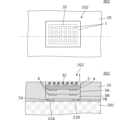
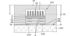
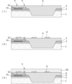
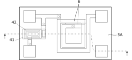
- FIG. 6 is a plan view of an electronic circuit device 302 according to the second embodiment, and the lower part of FIG. 6 is a vertical cross-sectional view taken along the dashed line in the plan view.
- FIG. 7 is a cross-sectional view of the chip part 102 before it is mounted on the circuit board 201.
- FIG. 8A to 8C are cross-sectional views showing a method for manufacturing the electronic circuit device 302 according to the second embodiment.
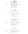
- FIG. 9 is a plan view showing a shape of the in-groove insulator 32 different from the example shown in FIG.
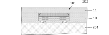
- FIG. 10 is a cross-sectional view of an electronic circuit device 303 according to the third embodiment.
- 11A to 11C are diagrams showing a method for manufacturing the electronic circuit device 304 according to the fourth embodiment.
- FIG. 12A to 12C are cross-sectional views showing a method for manufacturing an electronic circuit device according to the fifth embodiment.
- 13A to 13C are cross-sectional views showing a method for manufacturing an electronic circuit device according to the fifth embodiment.
- 14A to 14C are cross-sectional views showing a method for manufacturing an electronic circuit device according to the fifth embodiment.
- 15A to 15C are cross-sectional views showing a method for manufacturing an electronic circuit device according to the fifth embodiment.
- FIG. 16 is a plan view of the state shown in (10) in FIG.
- FIG. 17 is a circuit diagram of a circuit using electronic circuit device 305 configured in a predetermined position on a circuit board.
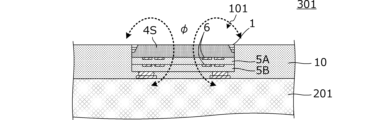
- First Embodiment 1 is a cross-sectional view of an electronic circuit device 301 according to the first embodiment.
- the electronic circuit device 301 includes a chip component 101, a circuit board 201, and a coating resin 10.
- the chip component 101 has an element substrate (described in detail later), an insulator exposed portion 4S, and insulator layers 5A and 5B.
- the insulator exposed portion 4S can be defined as an insulator embedded in the element substrate 1.
- the insulator exposed portion 4S will be described in detail later.
- the element substrate 1 has a first main surface and a second main surface that are opposite each other.
- the insulator exposed portion 4S is exposed on a surface that is continuous with the second main surface (top surface in FIG. 1) of the element substrate 1.
- the insulator layers 5A and 5B are formed with a coil conductor 6 that generates magnetic flux with a component in the vertical direction (up and down direction in FIG.
- the coil conductor 6 is formed in the stacking direction of the insulator exposed portion 4S and the insulator layers 5A and 5B to form a spiral, helical, or mixed spiral-helical coil.
- the chip component 101 has chip component side mounting electrodes 7A and 7B formed thereon, which connect the circuit to the circuit board 201.
- a continuous surface without sharp steps is formed on the surfaces of the insulator layer 4, the element substrate 1, and the coating resin 10.
- This "continuous surface” means a “flat surface,” “almost flat surface,” “flat and continuous surface,” etc.
- the above-mentioned “continuous surface” means a surface in which the proportion of acute-angled protrusions is smaller than the proportion of obtuse-angled protrusions.
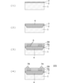
- This grinding exposes the insulator layer 4 to form the insulator exposed portion 4S. As a result, at least a portion of the coil opening formed by the coil conductor 6 is positioned within the insulator exposed portion 4S.
- FIG. 4 shows a coil conductor 6 that generates or receives a magnetic flux ⁇ component in a direction perpendicular to the exposed insulator portion 4S and insulator layers 5A and 5B.
- the area of the element substrate 1 of the chip component 101 is small, and the element substrate 1 is outside the coil opening, so the magnetic flux ⁇ is hardly blocked by the element substrate 1 of the chip component 101.
- the coating resin 10 is not magnetic.
- the circuit substrate 201 is also not magnetic, or contains almost no magnetic parts. This makes it possible to suppress losses due to eddy currents.
- the surface of the element substrate 1, the surface of the insulator exposed portion 4S, and the surface of the coating resin 10 form a continuous surface without sharp steps such as sharp points or recesses.
- the element substrate 1 is mounted on the circuit board while retaining a sufficient thickness, and the chip components and circuit board are fixed with a coating resin. After that, unnecessary Si substrate portions are removed. This makes it possible to mount the chip components, while ensuring mechanical strength when coated with the coating resin and improving electrical characteristics by suppressing eddy currents, and also to achieve a thinner overall circuit device.
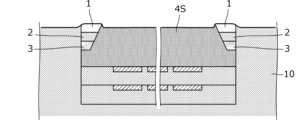
- the chip component 102 includes an element substrate 1, a passivation film 3, insulating layers 4, 5A, and 5B, a coil conductor 6, and chip component side mounting electrodes 7A and 7B.
- Chip component side mounting electrodes 7A and 7B are connected to circuit board side electrodes 21A and 21B of the circuit board 201.
- the mounting surface of the circuit board 201 on which the chip components 102 are mounted is covered with a coating resin 10.
- the groove insulators 32 are distributed on the element substrate 1, and the groove insulators 32 spread across the element substrate 1. Therefore, the area of the element substrate 1 of the chip component 102 is small. Also, the current loop of the eddy current flowing through the element substrate 1 is small. Therefore, losses due to eddy currents can be suppressed.
- FIG. 7 is a cross-sectional view of chip component 102 before it is mounted on circuit board 201 shown in FIG. 6.
- element substrate 1 such as a Si substrate
- a groove (trench) 30 is formed from the surface of element substrate 1, an inner surface of this groove is formed with groove insulator 31 made of an inorganic oxide film such as SiO2, and inside the groove is formed groove insulator 32 such as polysilicon.
- FIG. 8 is a cross-sectional view showing a manufacturing method of an electronic circuit device 302 according to the second embodiment.
- the chip component side mounting electrodes 7A, 7B of the chip component 102 are connected to the circuit board side electrodes 21A, 21B formed on the circuit board 201. That is, the chip component 102 is mounted on the mounting surface MS of the circuit board 201. For example, the chip component 102 is mounted at a position where the chip component side mounting electrodes 7A, 7B face the circuit board side electrodes 21A, 21B, and soldered by heating.
- chip component side mounting electrodes of the chip component 102 may be simply electrodes, and solder paste may be applied to the circuit board side electrodes 21A, 21B formed on the circuit board 201, the chip component side mounting electrodes 7A, 7B may be mounted, and soldered by heating.
- the mounting surface MS of the chip component on the circuit board 201 is coated with coating resin 10.
- the coating height of this coating resin 10 is higher than the top surface of the chip component 102.
- FIG. 9 is a plan view showing a shape of the groove insulator 32 different from the example shown in FIG. 6.
- a plurality of groove insulators 32 each extending horizontally are formed on the element substrate 1.
- a plurality of groove insulators 32 each extending vertically are formed on the element substrate 1. Even with such a pattern of groove insulators 32, the area of the element substrate 1 is small, and the current loop of the eddy current flowing through the element substrate 1 is small.
- the groove insulators 32 are formed in a vertical lattice shape on the element substrate 1.
- the groove insulators 32 are formed on the element substrate 1, each having a plurality of portions extending vertically and a portion connecting them horizontally. Even with this shape, the current loop of the eddy currents attempting to flow through the element substrate 1 is effectively made small.
- the grinding speed of SiO2 is slower than that of Si, so even if high speed processing is performed from the start of grinding to the trench, the grinding speed slows down when the trench is reached. Therefore, while high speed processing can shorten the time required for manufacturing, the amount of grinding can be controlled with high precision after the trench is reached.
- FIG. 10 is a cross-sectional view of an electronic circuit device 303 according to the third embodiment.
- chip components 101 are mounted on a circuit board 201, the mounting surface of the circuit board 201 on which the chip components 101 are mounted is covered with a coating resin 10, and the upper surfaces of the chip components 101 and the coating resin 10 are covered with an outer protective coating resin 11.
- This electronic circuit device 303 has a structure in which the upper surface of the electronic circuit device 301 shown in FIG. 1 is further coated with an outer protective resin 11.
- the chip component 101 mounted on the circuit board 201 may be covered with a coating resin 10 and an outer protective resin 11. This improves the external environment of the chip component 101 while maintaining the thinness and flatness of the electronic circuit device 303.
- the chip component side mounting electrodes 7A, 7B of the chip component 101 are connected to the circuit board side electrodes 21A, 21B formed on the circuit board 201. In other words, the chip component 101 is mounted on the mounting surface MS of the circuit board 201.
- the mounting surface MS of the chip component 101 on the circuit board 201 is coated with the coating resin 10.
- the planar coverage of the coating resin 10 is large enough to cover the chip component 101.
- the height of the coating resin 10 is higher than the top surface of the chip component 101.
- the coating resin 10, element substrate 1, and insulator layer 4 are ground to a depth that will later become the chip surface CS. This removes a portion of the element substrate 1 and insulator layer 4 of the chip component 101.
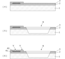
- FIG. 12 is a cross-sectional view showing a method for manufacturing an electronic circuit device according to the fifth embodiment.
- Numbers (1) to (12) in FIGS. 12 to 15 indicate the general process steps. Hereinafter, the process steps will be explained in numerical order.
- An element substrate 1, such as a Si substrate, is placed in the manufacturing equipment.
- An oxide film 2 such as SiO2 is formed on the surface of the element substrate 1.
- a capacitor electrode 41 is formed on the surface of the oxide film 2 and shaped into a predetermined pattern.
- a dielectric layer 40 is formed on the upper surface of the capacitor electrode 41 and shaped into a predetermined pattern.
- a capacitor electrode 42 is formed on the upper surface of the dielectric layer 40 and shaped into a predetermined pattern.
- a capacitor is formed by the dielectric layer 40 and the capacitor electrodes 41 and 42.
- a passivation film 3 is formed over the entire area including the capacitor by CVD or other methods.
- a recess R of a predetermined depth is formed from the surface of the passivation film 3 to the element substrate 1 by, for example, dry etching or sandblasting.
- Holes (vias) V reaching the capacitor electrodes 41 and 42 are formed, for example, by trial etching. Note that the recesses shown in (5) may be formed after these holes V are formed.
- An insulating layer 4 is formed from the bottom surface of the recess R to a position at a predetermined height above the passivation film 3.
- This insulating layer 4 is an organic insulating film for leveling purposes that flatten the surface, and is, for example, a photosensitive organic film such as epoxy resin, polyimide-polybenzoxazole (PBO), or polyimide (PI).
- a first layer of the conductor or coil conductor 6 is formed, which is connected to the hole (via) V that reaches the capacitor electrodes 41, 42.
- a Cu film is formed to a thickness of 1 ⁇ m or more, and then Ti, TiN is formed on the surface to a thickness of 10 nm to 100 nm.
- An adhesive layer may also be formed between the Cu film or Al film and the insulator layer 4.
- the coil conductor 6 is formed by semi-additive plating (SAP), lift-off, wet etching, etc.
- An insulator layer 5A such as an organic insulating film is formed over the entire upper area of the conductor that is conductive to the capacitor electrodes 41, 42 and the first layer of the coil conductor 6, and a hole (via) V that is conductive to the capacitor electrode 41 is formed.
- An insulator layer 5B such as an organic insulating film is formed over the entire upper area of the second layer of the conductor and coil conductor 6 that are conductive to the capacitor electrodes 41 and 42, and a hole (via) V is formed to provide electrical conductivity to the chip component side mounting electrode.
- the chip component 105 is mounted on a circuit board, and the insulator layer 4 is left open with no element substrate 1 present, for example in the same manner as in the process shown in FIG. 3.
- FIG. 17 is a circuit diagram of a circuit using the electronic circuit device 305 of this embodiment configured at a predetermined position on a circuit board.
- the circuit has the ends of an inductor L and a capacitor C connected to each other.
- This chip component 105 can be used as an element in which an inductor L and a capacitor C are connected in series, or as an element in which they are connected in parallel.
- the covering height of the coating resin 10 on the circuit board 201 is higher than the height of the chip components, but the covering height of the coating resin 10 on the circuit board 201 may be substantially the same height as the upper surface of the chip components. Even in this case, when the element substrate 1 of the chip components is ground to expose the insulator layer while the chip components are mounted on the circuit board 201, the stress on the chip components can be suppressed.
- the above explanation describes the coil conductor 6 generating magnetic flux and the generation of eddy currents due to that magnetic flux, but if the coil formed by the coil conductor receives a magnetic flux component perpendicular to the insulating layer, the generation of eddy currents due to that magnetic flux can be similarly suppressed.
- the entire coil opening was present within the area formed by the exposed insulator portion 4S when viewed in the stacking direction of the element substrate 1 and the insulator layers 5A and 5B.
- the eddy current suppression effect of the Si substrate is achieved.
- the entire coil opening was within the formation area of the insulator exposed portion when viewed in the stacking direction of the element substrate 1 and the insulator layers 5A and 5B, but even if at least a portion of the coil opening of the coil conductor is only within the formation area of the insulator exposed portion when viewed in the stacking direction, the effect of suppressing eddy currents by the Si substrate is achieved.
- Figures 3, 6, 8, 11, etc. show the vicinity of a single chip component, multiple chip components can be mounted on a circuit board and the chip components can be ground simultaneously.
- a capacitor is shown as an example of a circuit element other than a coil conductor at the position where the element substrate 1 is present when viewed in the stacking direction of the element substrate 1 and the insulator layers, but other elements may also be formed.
- diodes, transistors, and MOS capacitors may be formed using part of the element substrate 1 as circuit elements other than the coil conductor.
- the electronic circuit device and manufacturing method of the present invention may be provided in the following forms:
- the device includes a chip component, a circuit board, and a coating resin
- the chip part is an element substrate having a first main surface and a second main surface in an opposing relationship; an insulating layer formed on the first main surface side of the element substrate; a coil conductor formed inside the insulator layer and configured to generate or receive a magnetic flux having a component perpendicular to the first main surface of the element substrate; a chip component side mounting electrode formed on the first main surface side and connecting the coil conductor or a circuit including the coil conductor to the circuit board; having the circuit board has circuit-board electrodes to which the chip component mounting electrodes are connected, the chip component side mounting electrodes are connected to the circuit board side electrodes, the coating resin is formed to coat a mounting surface of the circuit board on which the chip component is mounted, an insulator exposed portion at which the insulator layer surrounded by the element substrate is exposed; the second main surface of the element substrate, the insulator exposed portion, and a surface including the coating resin form a continuous surface; at least
- the insulator exposed portion has an area of the second main surface smaller than an area of the first main surface of the element substrate;
- a circuit element other than the coil conductor is formed at a position where the element substrate is present as viewed in a direction perpendicular to the second main surface;
- the element substrate is a semiconductor substrate.
- a chip component is constructed by forming a recess or an opening on a side of a first main surface of an element substrate having a first main surface and a second main surface that are opposed to each other, forming an insulator inside the recess or the opening, forming an insulator layer on the side of the first main surface of the element substrate, forming a coil conductor in the insulator layer that generates or receives a magnetic flux having a perpendicular component to the insulator layer, and forming a chip component-side mounting electrode on a circuit board that connects the coil conductor or a circuit including the coil conductor, forming a circuit board side electrode to which the chip component side mounting electrode is connected on the circuit board;
- the chip component side mounting electrodes are connected to the circuit board side electrodes, a coating resin is applied to a mounting surface of the chip component on the circuit board;
- the element substrate and the insulator layer are ground from the second main surface side until the insulator inside the recess or the opening is exposed from the
Landscapes
- Engineering & Computer Science (AREA)
- Power Engineering (AREA)
- Microelectronics & Electronic Packaging (AREA)
- Manufacturing & Machinery (AREA)
- Coils Or Transformers For Communication (AREA)
Abstract
Un dispositif de circuit électronique (301) comprend un composant de puce (101), une carte de circuit imprimé (201) et une résine de revêtement (10). Le composant de puce (101) est monté sur la carte de circuit imprimé (201), et la résine de revêtement (10) est appliquée pour revêtir une surface de montage de la carte de circuit imprimé (201). La surface d'un substrat d'élément (1), la surface d'une couche isolante et la surface de la résine de revêtement (10) constituent une surface continue dans laquelle, vue dans la direction de stratification du substrat d'élément (1) et de la couche isolante, il y a une partie exposée d'isolant (4S) où aucun substrat d'élément (1) n'est présent en raison de l'exposition de la couche isolante. Au moins une partie d'une ouverture de bobine formée par un conducteur de bobine (6) est située à l'intérieur de la zone de la partie exposée d'isolant (4S).
Priority Applications (3)
| Application Number | Priority Date | Filing Date | Title |
|---|---|---|---|
| CN202480038562.7A CN121312327A (zh) | 2023-06-13 | 2024-05-23 | 电子电路装置及其制造方法 |
| JP2025527608A JPWO2024257574A1 (fr) | 2023-06-13 | 2024-05-23 | |
| US19/411,892 US20260096028A1 (en) | 2023-06-13 | 2025-12-08 | Electronic circuit device and method for manufacturing the same |
Applications Claiming Priority (2)
| Application Number | Priority Date | Filing Date | Title |
|---|---|---|---|
| JP2023-096990 | 2023-06-13 | ||
| JP2023096990 | 2023-06-13 |
Related Child Applications (1)
| Application Number | Title | Priority Date | Filing Date |
|---|---|---|---|
| US19/411,892 Continuation US20260096028A1 (en) | 2023-06-13 | 2025-12-08 | Electronic circuit device and method for manufacturing the same |
Publications (1)
| Publication Number | Publication Date |
|---|---|
| WO2024257574A1 true WO2024257574A1 (fr) | 2024-12-19 |
Family
ID=93851789
Family Applications (1)
| Application Number | Title | Priority Date | Filing Date |
|---|---|---|---|
| PCT/JP2024/018969 Ceased WO2024257574A1 (fr) | 2023-06-13 | 2024-05-23 | Dispositif de circuit électronique et procédé de fabrication de celui-ci |
Country Status (4)
| Country | Link |
|---|---|
| US (1) | US20260096028A1 (fr) |
| JP (1) | JPWO2024257574A1 (fr) |
| CN (1) | CN121312327A (fr) |
| WO (1) | WO2024257574A1 (fr) |
Citations (5)
| Publication number | Priority date | Publication date | Assignee | Title |
|---|---|---|---|---|
| JPS6464240A (en) * | 1987-09-03 | 1989-03-10 | Tdk Corp | Ic package |
| JPH0555043A (ja) * | 1991-08-22 | 1993-03-05 | Fujitsu Ltd | 小型コイルとその製造方法,磁気ヘツドの製造方法及び磁気記憶装置 |
| US5844299A (en) * | 1997-01-31 | 1998-12-01 | National Semiconductor Corporation | Integrated inductor |
| JP2002343904A (ja) * | 2001-05-21 | 2002-11-29 | Matsushita Electric Ind Co Ltd | 半導体装置 |
| US20050040430A1 (en) * | 2001-12-11 | 2005-02-24 | Infineon Technologies Ag | Diode circuit and method of producing a diode circuit |
-
2024
- 2024-05-23 CN CN202480038562.7A patent/CN121312327A/zh active Pending
- 2024-05-23 WO PCT/JP2024/018969 patent/WO2024257574A1/fr not_active Ceased
- 2024-05-23 JP JP2025527608A patent/JPWO2024257574A1/ja active Pending
-
2025
- 2025-12-08 US US19/411,892 patent/US20260096028A1/en active Pending
Patent Citations (5)
| Publication number | Priority date | Publication date | Assignee | Title |
|---|---|---|---|---|
| JPS6464240A (en) * | 1987-09-03 | 1989-03-10 | Tdk Corp | Ic package |
| JPH0555043A (ja) * | 1991-08-22 | 1993-03-05 | Fujitsu Ltd | 小型コイルとその製造方法,磁気ヘツドの製造方法及び磁気記憶装置 |
| US5844299A (en) * | 1997-01-31 | 1998-12-01 | National Semiconductor Corporation | Integrated inductor |
| JP2002343904A (ja) * | 2001-05-21 | 2002-11-29 | Matsushita Electric Ind Co Ltd | 半導体装置 |
| US20050040430A1 (en) * | 2001-12-11 | 2005-02-24 | Infineon Technologies Ag | Diode circuit and method of producing a diode circuit |
Also Published As
| Publication number | Publication date |
|---|---|
| JPWO2024257574A1 (fr) | 2024-12-19 |
| US20260096028A1 (en) | 2026-04-02 |
| CN121312327A (zh) | 2026-01-09 |
Similar Documents
| Publication | Publication Date | Title |
|---|---|---|
| KR102440119B1 (ko) | 반도체 패키지 및 그 제조방법 | |
| TW464996B (en) | Semiconductor device and its manufacturing process | |
| KR101059334B1 (ko) | 반도체 장치 및 그 실장 구조와, 그 제조 방법 | |
| US9147587B2 (en) | Interconnect substrate with embedded semiconductor device and built-in stopper and method of making the same | |
| JP2005327984A (ja) | 電子部品及び電子部品実装構造の製造方法 | |
| US20160351504A1 (en) | Semiconductor package and mounting structure thereof | |
| US9633989B2 (en) | ESD protection device | |
| US20170236765A1 (en) | Chip part and method for manufacturing a chip part | |
| US9087847B2 (en) | Thermally enhanced interconnect substrate with embedded semiconductor device and built-in stopper and method of making the same | |
| KR20080084572A (ko) | 반도체장치 및 그 제조방법 | |
| TW202145385A (zh) | 內埋元件的基板結構及其製造方法 | |
| WO2010050091A1 (fr) | Dispositif à semi-conducteur | |
| US12489068B2 (en) | Redistribution substrate having embedded inductor | |
| KR20160066311A (ko) | 반도체 패키지 및 반도체 패키지의 제조방법 | |
| TW202234603A (zh) | 貫通電極基板、半導體裝置及貫通電極基板之製造方法 | |
| JP7140530B2 (ja) | 電子部品およびその製造方法 | |
| TWI651741B (zh) | 附電容器之半導體裝置 | |
| TWI624011B (zh) | 封裝結構及其製法 | |
| CN108695299A (zh) | 电子封装件及其承载结构与制法 | |
| CN210467824U (zh) | 半导体封装结构 | |
| WO2024257574A1 (fr) | Dispositif de circuit électronique et procédé de fabrication de celui-ci | |
| CN102190279A (zh) | 半导体装置 | |
| JP2006049557A (ja) | 半導体装置 | |
| TW201611695A (zh) | 無核心層封裝基板與其製造方法 | |
| CN114078787B (zh) | 基板结构及其制法 |
Legal Events
| Date | Code | Title | Description |
|---|---|---|---|
| 121 | Ep: the epo has been informed by wipo that ep was designated in this application |
Ref document number: 24823196 Country of ref document: EP Kind code of ref document: A1 |
|
| ENP | Entry into the national phase |
Ref document number: 2025527608 Country of ref document: JP Kind code of ref document: A |
|
| WWE | Wipo information: entry into national phase |
Ref document number: 2025527608 Country of ref document: JP |
|
| NENP | Non-entry into the national phase |
Ref country code: DE |