WO2024257574A1 - 電子回路装置及びその製造方法 - Google Patents
電子回路装置及びその製造方法 Download PDFInfo
- Publication number
- WO2024257574A1 WO2024257574A1 PCT/JP2024/018969 JP2024018969W WO2024257574A1 WO 2024257574 A1 WO2024257574 A1 WO 2024257574A1 JP 2024018969 W JP2024018969 W JP 2024018969W WO 2024257574 A1 WO2024257574 A1 WO 2024257574A1
- Authority
- WO
- WIPO (PCT)
- Prior art keywords
- element substrate
- circuit board
- chip component
- main surface
- insulator
- Prior art date
- Legal status (The legal status is an assumption and is not a legal conclusion. Google has not performed a legal analysis and makes no representation as to the accuracy of the status listed.)
- Ceased
Links
Images







Classifications
-
- H—ELECTRICITY
- H05—ELECTRIC TECHNIQUES NOT OTHERWISE PROVIDED FOR
- H05K—PRINTED CIRCUITS; CASINGS OR CONSTRUCTIONAL DETAILS OF ELECTRIC APPARATUS; MANUFACTURE OF ASSEMBLAGES OF ELECTRICAL COMPONENTS
- H05K1/00—Printed circuits
- H05K1/18—Printed circuits structurally associated with non-printed electric components
- H05K1/181—Printed circuits structurally associated with non-printed electric components associated with surface mounted components
-
- H—ELECTRICITY
- H01—ELECTRIC ELEMENTS
- H01F—MAGNETS; INDUCTANCES; TRANSFORMERS; SELECTION OF MATERIALS FOR THEIR MAGNETIC PROPERTIES
- H01F17/00—Fixed inductances of the signal type
-
- H—ELECTRICITY
- H01—ELECTRIC ELEMENTS
- H01F—MAGNETS; INDUCTANCES; TRANSFORMERS; SELECTION OF MATERIALS FOR THEIR MAGNETIC PROPERTIES
- H01F27/00—Details of transformers or inductances, in general
- H01F27/06—Mounting, supporting or suspending transformers, reactors or choke coils not being of the signal type
-
- H—ELECTRICITY
- H01—ELECTRIC ELEMENTS
- H01F—MAGNETS; INDUCTANCES; TRANSFORMERS; SELECTION OF MATERIALS FOR THEIR MAGNETIC PROPERTIES
- H01F41/00—Apparatus or processes specially adapted for manufacturing or assembling magnets, inductances or transformers; Apparatus or processes specially adapted for manufacturing materials characterised by their magnetic properties
- H01F41/02—Apparatus or processes specially adapted for manufacturing or assembling magnets, inductances or transformers; Apparatus or processes specially adapted for manufacturing materials characterised by their magnetic properties for manufacturing cores, coils, or magnets
- H01F41/04—Apparatus or processes specially adapted for manufacturing or assembling magnets, inductances or transformers; Apparatus or processes specially adapted for manufacturing materials characterised by their magnetic properties for manufacturing cores, coils, or magnets for manufacturing coils
-
- H—ELECTRICITY
- H05—ELECTRIC TECHNIQUES NOT OTHERWISE PROVIDED FOR
- H05K—PRINTED CIRCUITS; CASINGS OR CONSTRUCTIONAL DETAILS OF ELECTRIC APPARATUS; MANUFACTURE OF ASSEMBLAGES OF ELECTRICAL COMPONENTS
- H05K3/00—Apparatus or processes for manufacturing printed circuits
- H05K3/22—Secondary treatment of printed circuits
- H05K3/28—Applying non-metallic protective coatings
- H05K3/284—Applying non-metallic protective coatings for encapsulating mounted components
-
- H—ELECTRICITY
- H10—SEMICONDUCTOR DEVICES; ELECTRIC SOLID-STATE DEVICES NOT OTHERWISE PROVIDED FOR
- H10W—GENERIC PACKAGES, INTERCONNECTIONS, CONNECTORS OR OTHER CONSTRUCTIONAL DETAILS OF DEVICES COVERED BY CLASS H10
- H10W70/00—Package substrates; Interposers; Redistribution layers [RDL]
- H10W70/60—Insulating or insulated package substrates; Interposers; Redistribution layers
-
- H—ELECTRICITY
- H10—SEMICONDUCTOR DEVICES; ELECTRIC SOLID-STATE DEVICES NOT OTHERWISE PROVIDED FOR
- H10W—GENERIC PACKAGES, INTERCONNECTIONS, CONNECTORS OR OTHER CONSTRUCTIONAL DETAILS OF DEVICES COVERED BY CLASS H10
- H10W90/00—Package configurations
-
- H—ELECTRICITY
- H05—ELECTRIC TECHNIQUES NOT OTHERWISE PROVIDED FOR
- H05K—PRINTED CIRCUITS; CASINGS OR CONSTRUCTIONAL DETAILS OF ELECTRIC APPARATUS; MANUFACTURE OF ASSEMBLAGES OF ELECTRICAL COMPONENTS
- H05K2201/00—Indexing scheme relating to printed circuits covered by H05K1/00
- H05K2201/10—Details of components or other objects attached to or integrated in a printed circuit board
- H05K2201/10007—Types of components
- H05K2201/1003—Non-printed inductor
Definitions
- the present invention relates to an electronic circuit device having a circuit board on which chip components are mounted, and a method for manufacturing the same.
- Patent Documents 1 and 2 disclose that loss due to eddy currents can be suppressed by replacing the portion that overlaps with the inductor in a planar view with an insulating material, without using the above-mentioned glass substrate or GaAs substrate.
- the object of the present invention is to provide an electronic circuit device and a manufacturing method thereof that suppresses the generation of eddy currents caused by providing an inductor in a chip component, as well as the stress and damage that occur when mounting the chip component on a circuit board.
- the device includes a chip component, a circuit board, and a coating resin
- the chip part is an element substrate having a first main surface and a second main surface in an opposing relationship; an insulating layer formed on the first main surface side of the element substrate; a coil conductor formed inside the insulator layer and configured to generate or receive a magnetic flux having a component perpendicular to the first main surface of the element substrate; a chip component side mounting electrode formed on the first main surface side and connecting the coil conductor or a circuit including the coil conductor to the circuit board; having the circuit board has circuit-board electrodes to which the chip component mounting electrodes are connected, the chip component side mounting electrodes are connected to the circuit board side electrodes, the coating resin is formed to coat a mounting surface of the circuit board on which the chip component is mounted, an insulator exposed portion at which the insulator layer surrounded by the element substrate is exposed; the second main surface of the element substrate, the insulator exposed portion, and a surface including the
- a method for manufacturing an electronic circuit device includes: a chip component is constructed by forming a recess or an opening on a side of a first main surface of an element substrate having a first main surface and a second main surface that are opposed to each other, forming an insulator inside the recess or the opening, forming an insulator layer on the side of the first main surface of the element substrate, forming a coil conductor in the insulator layer that generates or receives a magnetic flux having a perpendicular component to the insulator layer, and forming a chip component-side mounting electrode on a circuit board that connects the coil conductor or a circuit including the coil conductor, forming a circuit board side electrode to which the chip component side mounting electrode is connected on the circuit board;
- the chip component side mounting electrodes are connected to the circuit board side electrodes, a coating resin is applied to a mounting surface of the chip component on the circuit board;
- the element substrate and the insulator layer are ground from the second main surface side until
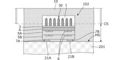
- FIG. 6 is a plan view of an electronic circuit device 302 according to the second embodiment, and the lower part of FIG. 6 is a vertical cross-sectional view taken along the dashed line in the plan view.
- FIG. 7 is a cross-sectional view of the chip part 102 before it is mounted on the circuit board 201.
- FIG. 8A to 8C are cross-sectional views showing a method for manufacturing the electronic circuit device 302 according to the second embodiment.
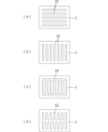
- FIG. 9 is a plan view showing a shape of the in-groove insulator 32 different from the example shown in FIG.
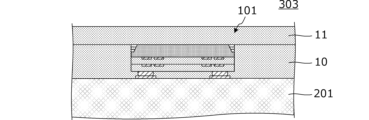
- FIG. 10 is a cross-sectional view of an electronic circuit device 303 according to the third embodiment.
- 11A to 11C are diagrams showing a method for manufacturing the electronic circuit device 304 according to the fourth embodiment.
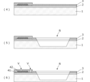
- FIG. 12A to 12C are cross-sectional views showing a method for manufacturing an electronic circuit device according to the fifth embodiment.
- 13A to 13C are cross-sectional views showing a method for manufacturing an electronic circuit device according to the fifth embodiment.
- 14A to 14C are cross-sectional views showing a method for manufacturing an electronic circuit device according to the fifth embodiment.
- 15A to 15C are cross-sectional views showing a method for manufacturing an electronic circuit device according to the fifth embodiment.
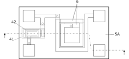
- FIG. 16 is a plan view of the state shown in (10) in FIG.
- FIG. 17 is a circuit diagram of a circuit using electronic circuit device 305 configured in a predetermined position on a circuit board.
- First Embodiment 1 is a cross-sectional view of an electronic circuit device 301 according to the first embodiment.
- the electronic circuit device 301 includes a chip component 101, a circuit board 201, and a coating resin 10.
- the chip component 101 has an element substrate (described in detail later), an insulator exposed portion 4S, and insulator layers 5A and 5B.
- the insulator exposed portion 4S can be defined as an insulator embedded in the element substrate 1.
- the insulator exposed portion 4S will be described in detail later.
- the element substrate 1 has a first main surface and a second main surface that are opposite each other.
- the insulator exposed portion 4S is exposed on a surface that is continuous with the second main surface (top surface in FIG. 1) of the element substrate 1.
- the insulator layers 5A and 5B are formed with a coil conductor 6 that generates magnetic flux with a component in the vertical direction (up and down direction in FIG.
- the coil conductor 6 is formed in the stacking direction of the insulator exposed portion 4S and the insulator layers 5A and 5B to form a spiral, helical, or mixed spiral-helical coil.
- the chip component 101 has chip component side mounting electrodes 7A and 7B formed thereon, which connect the circuit to the circuit board 201.
- a continuous surface without sharp steps is formed on the surfaces of the insulator layer 4, the element substrate 1, and the coating resin 10.
- This "continuous surface” means a “flat surface,” “almost flat surface,” “flat and continuous surface,” etc.
- the above-mentioned “continuous surface” means a surface in which the proportion of acute-angled protrusions is smaller than the proportion of obtuse-angled protrusions.
- This grinding exposes the insulator layer 4 to form the insulator exposed portion 4S. As a result, at least a portion of the coil opening formed by the coil conductor 6 is positioned within the insulator exposed portion 4S.
- FIG. 4 shows a coil conductor 6 that generates or receives a magnetic flux ⁇ component in a direction perpendicular to the exposed insulator portion 4S and insulator layers 5A and 5B.
- the area of the element substrate 1 of the chip component 101 is small, and the element substrate 1 is outside the coil opening, so the magnetic flux ⁇ is hardly blocked by the element substrate 1 of the chip component 101.
- the coating resin 10 is not magnetic.
- the circuit substrate 201 is also not magnetic, or contains almost no magnetic parts. This makes it possible to suppress losses due to eddy currents.
- the surface of the element substrate 1, the surface of the insulator exposed portion 4S, and the surface of the coating resin 10 form a continuous surface without sharp steps such as sharp points or recesses.
- the element substrate 1 is mounted on the circuit board while retaining a sufficient thickness, and the chip components and circuit board are fixed with a coating resin. After that, unnecessary Si substrate portions are removed. This makes it possible to mount the chip components, while ensuring mechanical strength when coated with the coating resin and improving electrical characteristics by suppressing eddy currents, and also to achieve a thinner overall circuit device.
- the chip component 102 includes an element substrate 1, a passivation film 3, insulating layers 4, 5A, and 5B, a coil conductor 6, and chip component side mounting electrodes 7A and 7B.
- Chip component side mounting electrodes 7A and 7B are connected to circuit board side electrodes 21A and 21B of the circuit board 201.
- the mounting surface of the circuit board 201 on which the chip components 102 are mounted is covered with a coating resin 10.
- the groove insulators 32 are distributed on the element substrate 1, and the groove insulators 32 spread across the element substrate 1. Therefore, the area of the element substrate 1 of the chip component 102 is small. Also, the current loop of the eddy current flowing through the element substrate 1 is small. Therefore, losses due to eddy currents can be suppressed.
- FIG. 7 is a cross-sectional view of chip component 102 before it is mounted on circuit board 201 shown in FIG. 6.
- element substrate 1 such as a Si substrate
- a groove (trench) 30 is formed from the surface of element substrate 1, an inner surface of this groove is formed with groove insulator 31 made of an inorganic oxide film such as SiO2, and inside the groove is formed groove insulator 32 such as polysilicon.
- FIG. 8 is a cross-sectional view showing a manufacturing method of an electronic circuit device 302 according to the second embodiment.
- the chip component side mounting electrodes 7A, 7B of the chip component 102 are connected to the circuit board side electrodes 21A, 21B formed on the circuit board 201. That is, the chip component 102 is mounted on the mounting surface MS of the circuit board 201. For example, the chip component 102 is mounted at a position where the chip component side mounting electrodes 7A, 7B face the circuit board side electrodes 21A, 21B, and soldered by heating.
- chip component side mounting electrodes of the chip component 102 may be simply electrodes, and solder paste may be applied to the circuit board side electrodes 21A, 21B formed on the circuit board 201, the chip component side mounting electrodes 7A, 7B may be mounted, and soldered by heating.
- the mounting surface MS of the chip component on the circuit board 201 is coated with coating resin 10.
- the coating height of this coating resin 10 is higher than the top surface of the chip component 102.
- FIG. 9 is a plan view showing a shape of the groove insulator 32 different from the example shown in FIG. 6.
- a plurality of groove insulators 32 each extending horizontally are formed on the element substrate 1.
- a plurality of groove insulators 32 each extending vertically are formed on the element substrate 1. Even with such a pattern of groove insulators 32, the area of the element substrate 1 is small, and the current loop of the eddy current flowing through the element substrate 1 is small.
- the groove insulators 32 are formed in a vertical lattice shape on the element substrate 1.
- the groove insulators 32 are formed on the element substrate 1, each having a plurality of portions extending vertically and a portion connecting them horizontally. Even with this shape, the current loop of the eddy currents attempting to flow through the element substrate 1 is effectively made small.
- the grinding speed of SiO2 is slower than that of Si, so even if high speed processing is performed from the start of grinding to the trench, the grinding speed slows down when the trench is reached. Therefore, while high speed processing can shorten the time required for manufacturing, the amount of grinding can be controlled with high precision after the trench is reached.
- FIG. 10 is a cross-sectional view of an electronic circuit device 303 according to the third embodiment.
- chip components 101 are mounted on a circuit board 201, the mounting surface of the circuit board 201 on which the chip components 101 are mounted is covered with a coating resin 10, and the upper surfaces of the chip components 101 and the coating resin 10 are covered with an outer protective coating resin 11.
- This electronic circuit device 303 has a structure in which the upper surface of the electronic circuit device 301 shown in FIG. 1 is further coated with an outer protective resin 11.
- the chip component 101 mounted on the circuit board 201 may be covered with a coating resin 10 and an outer protective resin 11. This improves the external environment of the chip component 101 while maintaining the thinness and flatness of the electronic circuit device 303.
- the chip component side mounting electrodes 7A, 7B of the chip component 101 are connected to the circuit board side electrodes 21A, 21B formed on the circuit board 201. In other words, the chip component 101 is mounted on the mounting surface MS of the circuit board 201.
- the mounting surface MS of the chip component 101 on the circuit board 201 is coated with the coating resin 10.
- the planar coverage of the coating resin 10 is large enough to cover the chip component 101.
- the height of the coating resin 10 is higher than the top surface of the chip component 101.
- the coating resin 10, element substrate 1, and insulator layer 4 are ground to a depth that will later become the chip surface CS. This removes a portion of the element substrate 1 and insulator layer 4 of the chip component 101.
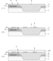
- FIG. 12 is a cross-sectional view showing a method for manufacturing an electronic circuit device according to the fifth embodiment.
- Numbers (1) to (12) in FIGS. 12 to 15 indicate the general process steps. Hereinafter, the process steps will be explained in numerical order.
- An element substrate 1, such as a Si substrate, is placed in the manufacturing equipment.
- An oxide film 2 such as SiO2 is formed on the surface of the element substrate 1.
- a capacitor electrode 41 is formed on the surface of the oxide film 2 and shaped into a predetermined pattern.
- a dielectric layer 40 is formed on the upper surface of the capacitor electrode 41 and shaped into a predetermined pattern.
- a capacitor electrode 42 is formed on the upper surface of the dielectric layer 40 and shaped into a predetermined pattern.
- a capacitor is formed by the dielectric layer 40 and the capacitor electrodes 41 and 42.
- a passivation film 3 is formed over the entire area including the capacitor by CVD or other methods.
- a recess R of a predetermined depth is formed from the surface of the passivation film 3 to the element substrate 1 by, for example, dry etching or sandblasting.
- Holes (vias) V reaching the capacitor electrodes 41 and 42 are formed, for example, by trial etching. Note that the recesses shown in (5) may be formed after these holes V are formed.
- An insulating layer 4 is formed from the bottom surface of the recess R to a position at a predetermined height above the passivation film 3.
- This insulating layer 4 is an organic insulating film for leveling purposes that flatten the surface, and is, for example, a photosensitive organic film such as epoxy resin, polyimide-polybenzoxazole (PBO), or polyimide (PI).
- a first layer of the conductor or coil conductor 6 is formed, which is connected to the hole (via) V that reaches the capacitor electrodes 41, 42.
- a Cu film is formed to a thickness of 1 ⁇ m or more, and then Ti, TiN is formed on the surface to a thickness of 10 nm to 100 nm.
- An adhesive layer may also be formed between the Cu film or Al film and the insulator layer 4.
- the coil conductor 6 is formed by semi-additive plating (SAP), lift-off, wet etching, etc.
- An insulator layer 5A such as an organic insulating film is formed over the entire upper area of the conductor that is conductive to the capacitor electrodes 41, 42 and the first layer of the coil conductor 6, and a hole (via) V that is conductive to the capacitor electrode 41 is formed.
- An insulator layer 5B such as an organic insulating film is formed over the entire upper area of the second layer of the conductor and coil conductor 6 that are conductive to the capacitor electrodes 41 and 42, and a hole (via) V is formed to provide electrical conductivity to the chip component side mounting electrode.
- the chip component 105 is mounted on a circuit board, and the insulator layer 4 is left open with no element substrate 1 present, for example in the same manner as in the process shown in FIG. 3.
- FIG. 17 is a circuit diagram of a circuit using the electronic circuit device 305 of this embodiment configured at a predetermined position on a circuit board.
- the circuit has the ends of an inductor L and a capacitor C connected to each other.
- This chip component 105 can be used as an element in which an inductor L and a capacitor C are connected in series, or as an element in which they are connected in parallel.
- the covering height of the coating resin 10 on the circuit board 201 is higher than the height of the chip components, but the covering height of the coating resin 10 on the circuit board 201 may be substantially the same height as the upper surface of the chip components. Even in this case, when the element substrate 1 of the chip components is ground to expose the insulator layer while the chip components are mounted on the circuit board 201, the stress on the chip components can be suppressed.
- the above explanation describes the coil conductor 6 generating magnetic flux and the generation of eddy currents due to that magnetic flux, but if the coil formed by the coil conductor receives a magnetic flux component perpendicular to the insulating layer, the generation of eddy currents due to that magnetic flux can be similarly suppressed.
- the entire coil opening was present within the area formed by the exposed insulator portion 4S when viewed in the stacking direction of the element substrate 1 and the insulator layers 5A and 5B.
- the eddy current suppression effect of the Si substrate is achieved.
- the entire coil opening was within the formation area of the insulator exposed portion when viewed in the stacking direction of the element substrate 1 and the insulator layers 5A and 5B, but even if at least a portion of the coil opening of the coil conductor is only within the formation area of the insulator exposed portion when viewed in the stacking direction, the effect of suppressing eddy currents by the Si substrate is achieved.
- Figures 3, 6, 8, 11, etc. show the vicinity of a single chip component, multiple chip components can be mounted on a circuit board and the chip components can be ground simultaneously.
- a capacitor is shown as an example of a circuit element other than a coil conductor at the position where the element substrate 1 is present when viewed in the stacking direction of the element substrate 1 and the insulator layers, but other elements may also be formed.
- diodes, transistors, and MOS capacitors may be formed using part of the element substrate 1 as circuit elements other than the coil conductor.
- the electronic circuit device and manufacturing method of the present invention may be provided in the following forms:
- the device includes a chip component, a circuit board, and a coating resin
- the chip part is an element substrate having a first main surface and a second main surface in an opposing relationship; an insulating layer formed on the first main surface side of the element substrate; a coil conductor formed inside the insulator layer and configured to generate or receive a magnetic flux having a component perpendicular to the first main surface of the element substrate; a chip component side mounting electrode formed on the first main surface side and connecting the coil conductor or a circuit including the coil conductor to the circuit board; having the circuit board has circuit-board electrodes to which the chip component mounting electrodes are connected, the chip component side mounting electrodes are connected to the circuit board side electrodes, the coating resin is formed to coat a mounting surface of the circuit board on which the chip component is mounted, an insulator exposed portion at which the insulator layer surrounded by the element substrate is exposed; the second main surface of the element substrate, the insulator exposed portion, and a surface including the coating resin form a continuous surface; at least
- the insulator exposed portion has an area of the second main surface smaller than an area of the first main surface of the element substrate;
- a circuit element other than the coil conductor is formed at a position where the element substrate is present as viewed in a direction perpendicular to the second main surface;
- the element substrate is a semiconductor substrate.
- a chip component is constructed by forming a recess or an opening on a side of a first main surface of an element substrate having a first main surface and a second main surface that are opposed to each other, forming an insulator inside the recess or the opening, forming an insulator layer on the side of the first main surface of the element substrate, forming a coil conductor in the insulator layer that generates or receives a magnetic flux having a perpendicular component to the insulator layer, and forming a chip component-side mounting electrode on a circuit board that connects the coil conductor or a circuit including the coil conductor, forming a circuit board side electrode to which the chip component side mounting electrode is connected on the circuit board;
- the chip component side mounting electrodes are connected to the circuit board side electrodes, a coating resin is applied to a mounting surface of the chip component on the circuit board;
- the element substrate and the insulator layer are ground from the second main surface side until the insulator inside the recess or the opening is exposed from the
Landscapes
- Engineering & Computer Science (AREA)
- Power Engineering (AREA)
- Microelectronics & Electronic Packaging (AREA)
- Manufacturing & Machinery (AREA)
- Coils Or Transformers For Communication (AREA)
Abstract
電子回路装置(301)は、チップ部品(101)と、回路基板(201)と、被覆樹脂(10)と、を備える。回路基板(201)にはチップ部品(101)が実装され、被覆樹脂(10)が回路基板(201)の実装面に被覆される。素子基板(1)の表面と絶縁体層の表面と被覆樹脂(10)の表面とは、連続面を成し、素子基板(1)及び絶縁体層の積層方向に視て、絶縁体層の露出による素子基板(1)の無い絶縁体露出部(4S)を有する。コイル導体(6)によるコイル開口部の少なくとも一部は絶縁体露出部(4S)の領域内にある。
Description
本発明は、チップ部品が搭載された回路基板を備える電子回路装置及びその製造方法に関する。
複数のパッシブコンポーネントを単一基板に集積して構成するIPD(Integrated Passive Device)素子は広く知られている。この基板としては、半導体素子の基板で一般的なSi基板が用いられる。又はSi基板にインダクタを形成した場合に、Si基板に渦電流が流れることによる損失を懸念して、ガラス基板やGaAs基板が用いられる。
一方、GaAs基板やガラス基板などの絶縁体基板を用いるとダイオードやMOSキャパシタなどの回路構成要素が構成できない。
上記ガラス基板やGaAs基板を用いることなく、インダクタと平面視で重なる部分を絶縁性材料に置き換えることで、渦電流による損失を抑制することが特許文献1、特許文献2に開示されている。
特許文献1、特許文献2に記載の集積回路装置では、Si基板に生じる渦電流による損失を抑制するために、平面視でインダクタに重なる部分のSi基板の一部を絶縁材料部材に置き換えている。
ところが、Si基板の一部を他の絶縁材料部材に置換すると、素子そのものが薄くなったり、Si基板のうち絶縁材料部材に置き換える部分が増加することで機械的な強度が低下したりする。これらのことにより、回路基板に対する上記集積回路装置の搭載時の応力や、リフローなどによる実装時の熱衝撃・応力により集積回路装置が破損するおそれがある。
そこで、本発明の目的は、チップ部品にインダクタを設けることによる渦電流の発生、及び回路基板へのチップ部品の搭載時の応力や実装時の破損を抑制した電子回路装置及びその製造方法を提供することにある。
(A)本開示の一例としての電子回路装置は、
チップ部品と、回路基板と、被覆樹脂と、を備え、
前記チップ部品は、
互いに反対面関係にある第1主面と第2主面とを有する素子基板と、
前記素子基板の前記第1主面の側に形成された絶縁体層と、
前記絶縁体層の内部に形成され、前記素子基板の前記第1主面の垂直方向成分を有する磁束を発生又は受けるコイル導体と、
前記第1主面の側に形成され前記回路基板に前記コイル導体又は当該コイル導体を含む回路を接続するチップ部品側実装電極と、
を有し、
前記回路基板は前記チップ部品側実装電極が接続される回路基板側電極を有し、
前記回路基板側電極に前記チップ部品側実装電極が接続され、
前記被覆樹脂は、前記チップ部品が実装される前記回路基板の実装面に被覆形成され、
前記素子基板に囲まれた前記絶縁体層が露出する絶縁体露出部を有し、
前記素子基板の前記第2主面、前記絶縁体露出部及び前記被覆樹脂を含む面は連続面を成し、
前記コイル導体によるコイル開口部の少なくとも一部は、前記素子基板の前記第2主面に垂直方向に視て前記絶縁体露出部の形成領域内にある、
ことを特徴とする。
チップ部品と、回路基板と、被覆樹脂と、を備え、
前記チップ部品は、
互いに反対面関係にある第1主面と第2主面とを有する素子基板と、
前記素子基板の前記第1主面の側に形成された絶縁体層と、
前記絶縁体層の内部に形成され、前記素子基板の前記第1主面の垂直方向成分を有する磁束を発生又は受けるコイル導体と、
前記第1主面の側に形成され前記回路基板に前記コイル導体又は当該コイル導体を含む回路を接続するチップ部品側実装電極と、
を有し、
前記回路基板は前記チップ部品側実装電極が接続される回路基板側電極を有し、
前記回路基板側電極に前記チップ部品側実装電極が接続され、
前記被覆樹脂は、前記チップ部品が実装される前記回路基板の実装面に被覆形成され、
前記素子基板に囲まれた前記絶縁体層が露出する絶縁体露出部を有し、
前記素子基板の前記第2主面、前記絶縁体露出部及び前記被覆樹脂を含む面は連続面を成し、
前記コイル導体によるコイル開口部の少なくとも一部は、前記素子基板の前記第2主面に垂直方向に視て前記絶縁体露出部の形成領域内にある、
ことを特徴とする。
(B)本開示の一例としての電子回路装置の製造方法は、
互いに反対面関係にある第1主面と第2主面とを有する素子基板の前記第1主面の側に凹部又は開口部を形成し、前記凹部又は前記開口部の内部に絶縁体を形成し、前記素子基板の前記第1主面の側に絶縁体層を形成し、前記絶縁体層に前記絶縁体層に対する垂直方向成分を有する磁束を発生又は受けるコイル導体を形成し、回路基板に前記コイル導体又は当該コイル導体を含む回路を接続するチップ部品側実装電極を形成する、ことでチップ部品を構成し、
前記チップ部品側実装電極が接続される回路基板側電極を前記回路基板に形成し、
前記回路基板側電極に前記チップ部品側実装電極を接続し、
前記回路基板への前記チップ部品の実装面に被覆樹脂を被覆し、
前記凹部又は前記開口部の内部の前記絶縁体が前記素子基板から露出するまで、前記素子基板及び前記絶縁体層を前記第2主面側から研削することで、前記素子基板の前記第2主面、前記凹部又は前記開口部の内部の前記絶縁体、及び前記被覆樹脂を含む面に連続面を形成する、
ことを特徴とする。
互いに反対面関係にある第1主面と第2主面とを有する素子基板の前記第1主面の側に凹部又は開口部を形成し、前記凹部又は前記開口部の内部に絶縁体を形成し、前記素子基板の前記第1主面の側に絶縁体層を形成し、前記絶縁体層に前記絶縁体層に対する垂直方向成分を有する磁束を発生又は受けるコイル導体を形成し、回路基板に前記コイル導体又は当該コイル導体を含む回路を接続するチップ部品側実装電極を形成する、ことでチップ部品を構成し、
前記チップ部品側実装電極が接続される回路基板側電極を前記回路基板に形成し、
前記回路基板側電極に前記チップ部品側実装電極を接続し、
前記回路基板への前記チップ部品の実装面に被覆樹脂を被覆し、
前記凹部又は前記開口部の内部の前記絶縁体が前記素子基板から露出するまで、前記素子基板及び前記絶縁体層を前記第2主面側から研削することで、前記素子基板の前記第2主面、前記凹部又は前記開口部の内部の前記絶縁体、及び前記被覆樹脂を含む面に連続面を形成する、
ことを特徴とする。
本発明によれば、チップ部品にインダクタを設けることによる渦電流の発生、及び回路基板へのチップ部品の搭載時の応力や実装時の破損を抑制した電子回路装置及びその製造方法が得られる。
以降、図を参照して幾つかの具体的な例を挙げて、本発明を実施するための複数の形態を示す。各図中には同一箇所に同一符号を付している。要点の説明又は理解の容易性を考慮して、実施形態を説明の便宜上、複数の実施形態に分けて示すが、異なる実施形態で示した構成の部分的な置換又は組み合わせは可能である。第2の実施形態以降では第1の実施形態と共通の事柄についての記述を省略し、異なる点についてのみ説明する。特に、同様の構成による同様の作用効果については実施形態毎には逐次言及しない。
《第1の実施形態》
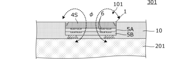
図1は第1の実施形態に係る電子回路装置301の断面図である。この電子回路装置301はチップ部品101と、回路基板201と、被覆樹脂10と、を備えている。
図1は第1の実施形態に係る電子回路装置301の断面図である。この電子回路装置301はチップ部品101と、回路基板201と、被覆樹脂10と、を備えている。
チップ部品101は、素子基板(後に詳細に示す。)1と、絶縁体露出部4Sと、絶縁体層5A,5Bとを有する。絶縁体露出部4Sは素子基板1に埋め込まれた絶縁体と定義できる。絶縁体露出部4Sについては後に詳細に示す。素子基板1は互いに反対面関係にある第1主面と第2主面とを有する。絶縁体露出部4Sは素子基板1の第2主面(図1における上面)に連続する面で露出する。また、絶縁体層5A,5Bには、素子基板1の第1主面の垂直方向(図1における上下方向)成分の磁束を発生又はその方向の磁束成分を受けるコイル導体6が形成されている。コイル導体6は、絶縁体露出部4S及び絶縁体層5A,5Bの積層方向に形成されて、スパイラル状、ヘリカル状又はスパイラル状ヘリカル状混在のコイルを形成する。
また、チップ部品101には、回路基板201に回路を接続するチップ部品側実装電極7A,7Bが形成されている。
回路基板201には、チップ部品101のチップ部品側実装電極7A,7Bが接続される回路基板側電極21A,21Bが形成されている。
回路基板201の回路基板側電極21A,21Bにはチップ部品側実装電極7A,7Bがそれぞれ接続されている。
チップ部品101が実装される回路基板201の実装面にはチップ部品101を取り囲むように被覆樹脂10が被覆されている。
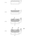
図2及び図3は第1の実施形態に係る電子回路装置301の製造方法について示す断面図である。図2及び図3に示す(1)から(7)は概略的な工程の手順を示す番号である。但し、(1)から(4)までは説明の都合上、単一のチップ部品の状態で図示しているが、実際は複数のチップ部品が並んだウエハー状態で製造する。また、(5)から(7)は単一のチップ部品に分離した後の状態で、電子回路装置の部分について図示している。以降、工程の番号順にその内容を説明する。
(1)例えばSi基板等の素子基板1の表面にSiO2等の酸化膜2を形成、その表面に窒化膜(Si2N4)等のパッシベーション膜をCVD等で形成する。
(2)パッシベーション膜表面から素子基板1まで所定深さの凹部を形成し、その凹部の底面からパッシベーション膜より所定高さの位置まで絶縁体層4を例えばドライエッチングやサンドブラストで形成する。この絶縁体層4はその表面を平坦化するレベリング用の有機絶縁膜であって、例えば、エポキシ樹脂、ポリイミド・ポリベンゾオキサゾール(PBO)、ポリイミド(PI)等の有機膜である。
(3)絶縁体層4の表面に絶縁体層5A,5Bを形成するとともにCuやAl等の導体部材でコイル導体6を形成する。これらコイル導体6の上下の表面に例えばTi,TiNを10nmから100nm形成する。このTi,TiN膜の成膜により、樹脂層との密着力が向上する。
(4)表面の絶縁体層5Bの表面に、はんだ等によるチップ部品側実装電極7A,7Bを形成する。この(4)までの工程によりチップ部品101の主要部を構成する。なお、図2中の(4)及びそれ以降の図4まではチップ部品側実装電極7A,7Bとコイル導体6との接続部のパターンは図示を省略している。コイル導体6の平面形状や層間接続及びチップ部品側実装電極7A,7Bとの接続構造については後に具体例を示す。
(5)回路基板201に形成した回路基板側電極21A,21Bにチップ部品101のチップ部品側実装電極7A,7Bをそれぞれ接続する。すなわち、回路基板201の実装面MSにチップ部品101を実装する。例えば、回路基板側電極21A,21Bにチップ部品側実装電極7A,7Bが対向する位置にチップ部品101を搭載し、加熱することによりはんだ付けする。なお、チップ部品101のチップ部品側実装電極は単なる電極とし、回路基板201に形成した回路基板側電極21A,21Bにはんだペーストを塗布し、チップ部品側実装電極7A,7Bを搭載し、加熱することではんだ付けしてもよい。
(6)回路基板201へのチップ部品101の実装面MSに被覆樹脂10を被覆する。この被覆樹脂10の被覆高さはチップ部品101の上面より高い。
(7)図3中で(6)に図示したように、後にチップ表面CSとなる深さまで被覆樹脂10、素子基板1及び絶縁体層4を研削する。このことにより、チップ部品101の素子基板1及び絶縁体層4の一部を削除する。このように絶縁体露出部4Sは素子基板1に埋め込まれた絶縁体層4の露出部と定義できる。
この研削工程により、後に詳細に示すように、絶縁体層4、素子基板1及び被覆樹脂10の表面に角張った段差部の無い連続面(研削面)を形成する。この「連続面」とは「平坦状の面」、「ほぼ平坦な面」、「平坦状に連続する面」などといった意味である。また、鋭角突起部や鈍角突起部等の種々の角度の突起部がある場合、上記「連続面」は、鋭角突起部の割合が鈍角突起部の割合より小さい面といった意味である。上記段差部については後に詳述する。この研削により絶縁体層4を露出させて絶縁体露出部4Sを形成する。このことにより、コイル導体6によるコイル開口部の少なくとも一部を絶縁体露出部4S内に配置する。
上述のとおり、チップ表面CSとなる深さまで被覆樹脂10、素子基板1及び絶縁体層4を研削すれば、絶縁体層4を露出させて絶縁体露出部4Sを形成できるが、素子基板の無い絶縁体露出部4Sがコイル導体6から素子基板1の方向へ先細り形状であることを利用してもよい。つまり、図2中の(3)から図3中の(7)等に示したように、絶縁体露出部4Sは素子基板1の第1主面における面積より、素子基板1の第2主面における面積の方が小さいため、すなわち先細り形状であるため、図3中で(6)(7)に示したように、チップ部品101の研削量に応じて絶縁体層4の露出面積が変化する。そのため、この露出面積が適正になるように被覆樹脂10及びチップ部品101の研削量を容易に定めることができる。
図4は、絶縁体露出部4S、絶縁体層5A,5Bに対する垂直方向に磁束φ成分を発生又は受けるコイル導体6を示す図である。チップ部品101の素子基板1の面積は小さく、素子基板1はコイル開口部の外側にあるので、磁束φはチップ部品101の素子基板1でほとんど遮られない。また、被覆樹脂10は磁性体ではない。回路基板201も磁性体ではない、又は磁性体部を殆ど含まない。そのため、渦電流による損失を抑制できる。
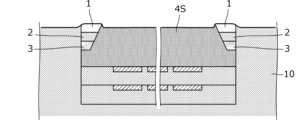
図5は、素子基板1の表面、絶縁体露出部4Sの表面及び被覆樹脂10の表面の位置関係や形状を示す図である。この図5に表れているように、素子基板1はSi基板等であり、絶縁体樹脂に比べて硬質であるので、図3中に(6)(7)で示したように、チップ表面CSとなる深さまで被覆樹脂10、素子基板1及び絶縁体層4を同時に研削すると、素子基板1は被覆樹脂10及び絶縁体露出部4Sより突出した状態となる。但し、素子基板1と絶縁体露出部4Sと被覆樹脂10とは一体化されたものであるので、素子基板1の表面と絶縁体露出部4Sの表面と被覆樹脂10の表面とは尖りや凹みといった角張った段差部の無い連続面を成している。この「連続面」とは、既に記述したとおり、例えば「平坦状の面」、「ほぼ平坦な面」、「平坦状に連続する面」などといった意味である。つまり、素子基板1が突出していても、「素子基板1の表面、絶縁体露出部4Sの表面及び被覆樹脂10の表面が連続面を成している」ことに相当する。また、研削は面で行っていくため、素子基板1が大きく突出している場合は、素子基板1のみを研削していくため、電子回路装置全体として見た時はほぼ平坦な連続面となっている。
本実施形態によれば、素子基板1が十分な厚みを持った状態で回路基板に実装し、被覆樹脂でチップ部品と回路基板を固定したのち、不要なSi基板部を除去することにより、チップ部品の実装と、被覆樹脂の被覆時の機械的強度の確保と渦電流の抑制による電気的特性の向上とを両立でき、さらには回路装置全体での薄型化も実現できる。
《第2の実施形態》
第2の実施形態では、素子基板の内部に絶縁体形成部が形成されて、素子基板の内部から絶縁体形成部の露出された絶縁体露出部を有するチップ部品及び電子回路装置について例示する。
第2の実施形態では、素子基板の内部に絶縁体形成部が形成されて、素子基板の内部から絶縁体形成部の露出された絶縁体露出部を有するチップ部品及び電子回路装置について例示する。
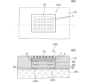
図6の上部は、第2の実施形態に係る電子回路装置302の平面図であり、図6の下部は上記平面図における一点鎖線での縦断面図である。
電子回路装置302は、チップ部品102と、回路基板201と、被覆樹脂10と、を備える。
チップ部品102は、素子基板1、パッシベーション膜3、絶縁体層4,5A,5B、コイル導体6及びチップ部品側実装電極7A,7B等を備える。
素子基板1の表面には溝内絶縁体32が露出している。コイル導体6は絶縁体層4及び絶縁体層5Aに形成されていて、絶縁体層4に対する垂直方向(図1における上下方向)に磁束成分を発生又はその方向の磁束成分を受ける。コイル導体6は、絶縁体層4,5A,5Bの積層方向に形成されて、スパイラル状又はヘリカル状のコイル回路を形成する。
回路基板201には、チップ部品102のチップ部品側実装電極7A,7Bが接続される回路基板側電極21A,21Bが形成されている。
回路基板201の回路基板側電極21A,21Bにはチップ部品側実装電極7A,7Bが接続されている。
チップ部品102が実装される回路基板201の実装面には被覆樹脂10が被覆されている。
このように、素子基板1に溝内絶縁体32が分布していて、また素子基板1に溝内絶縁体32が拡がっている。このため、チップ部品102の素子基板1の面積は小さい。また、素子基板1に流れようとする渦電流の電流ループは小さなものとなる。そのため、渦電流による損失を抑制できる。
図7は、図6に示した回路基板201に実装される前の状態でのチップ部品102の断面図である。Si基板等の素子基板1の内部には素子基板1の表面から溝(トレンチ)30が形成されていて、この溝の内面にSiO2等の無機酸化膜による溝内絶縁体31が形成されていて、溝の内部にポリシリコン等の溝内絶縁体32が形成されている。
素子基板1の上面にはパッシベーション膜3が形成されていて、その状部に絶縁体層4,5A,5Bが形成されている。絶縁体層4の上面及び絶縁体層5Aの上面にコイル導体6が形成されている。絶縁体層5Bの上面にはチップ部品側実装電極7A,7Bが形成されている。
図8は第2の実施形態に係る電子回路装置302の製造方法について示す断面図である。まず、回路基板201に形成した回路基板側電極21A,21Bに、チップ部品102のチップ部品側実装電極7A,7Bを接続する。すなわち、回路基板201の実装面MSにチップ部品102を実装する。例えば、回路基板側電極21A,21Bにチップ部品側実装電極7A,7Bが対向する位置にチップ部品102を搭載し、加熱することによりはんだ付けする。なお、チップ部品102のチップ部品側実装電極は単なる電極とし、回路基板201に形成した回路基板側電極21A,21Bにはんだペーストを塗布し、チップ部品側実装電極7A,7Bを搭載し、加熱することではんだ付けしてもよい。
次に、回路基板201へのチップ部品の実装面MSに被覆樹脂10を被覆する。この被覆樹脂10の被覆高さはチップ部品102の上面より高い。
図8に図示したように、後にチップ表面CSとなる深さまで被覆樹脂10、素子基板1及び溝30を研削する。このことにより、チップ部品102の素子基板1及び溝内絶縁体31,32の一部を削除する。このことにより、溝内絶縁体31,32、素子基板1及び被覆樹脂10の表面に、角張った段差部の無い連続面(研削面)を形成する。被覆樹脂10の研削により溝内絶縁体31,32を露出させて溝内絶縁体31,32の露出部を形成する。このことにより、コイル導体6によるコイル開口部の少なくとも一部が、素子基板1及び絶縁体層4,5A,5Bの積層方向に視て、絶縁体露出部の形成領域内にある。
なお、図6から図8まではチップ部品側実装電極7A,7Bとコイル導体6との接続部のパターンは図示を省略している。
図9は図6に示した例とは異なる溝内絶縁体32の形状を示す平面図である。図9において、(a)で示すチップ部品では、素子基板1にそれぞれ横長に延伸した複数の溝内絶縁体32が形成されている。(b)で示すチップ部品では、素子基板1にそれぞれ縦長に延伸した複数の溝内絶縁体32が形成されている。これらのような溝内絶縁体32のパターンであっても、素子基板1の面積は小さく、素子基板1に流れようとする渦電流の電流ループは小さなものとなる。(c)で示す部品では、素子基板1に縦格子状の溝内絶縁体32が形成されている。このように、素子基板1に流れる渦電流路を溝内絶縁体32で閉じることにより、素子基板1に流れようとする渦電流の電流ループは効果的に小さなものとなる。(d)で示す部品では、素子基板1にそれぞれ縦方向に延伸する複数の部分とそれらを横方向に連続させる部分を有する溝内絶縁体32が形成されている。このような形状であっても、素子基板1に流れようとする渦電流の電流ループは効果的に小さなものとなる。
本実施形態によれば、Siに比べてSiO2の研削速度は遅いので、研削の開始からトレンチに至るまで高速で処理しても、トレンチに達したところで研削速度が遅くなる。そのため、高速処理で製造に必要な時間を短縮しつつも、トレンチに達した以降は研削量を高精度に制御できる。
《第3の実施形態》
第3の実施形態ではチップ部品を密封した電子回路装置について例示する。
第3の実施形態ではチップ部品を密封した電子回路装置について例示する。
図10は第3の実施形態に係る電子回路装置303の断面図である。この電子回路装置303は、回路基板201にチップ部品101が実装されていて、チップ部品101が実装されている回路基板201の実装面に被覆樹脂10が被覆されていて、チップ部品101及び被覆樹脂10の上面に外被保護樹脂11が被覆されている。
この電子回路装置303は図1に示した電子回路装置301の上面に外被保護樹脂11をさらに被覆した構造を成している。
本実施形態で示すように、回路基板201に実装したチップ部品101を被覆樹脂10及び外被保護樹脂11で被覆してもよい。これにより、電子回路装置303の薄型化や平坦性を保ちつつチップ部品101の外的環境が向上する。
《第4の実施形態》
第4の実施形態では、これまでに示した実施形態とは異なる被覆樹脂の形状及びその形成方法について例示する。
第4の実施形態では、これまでに示した実施形態とは異なる被覆樹脂の形状及びその形成方法について例示する。
図11に示す(1)から(4)は概略的な工程の手順を示す番号である。以降、工程の番号順にその内容を説明する。
(1)回路基板201に形成した回路基板側電極21A,21Bにチップ部品101のチップ部品側実装電極7A,7Bを接続する。すなわち、回路基板201の実装面MSにチップ部品101を実装する。
(2)回路基板201へのチップ部品101の実装面MSに被覆樹脂10を被覆する。この被覆樹脂10の被覆平面範囲はチップ部品101を覆う広さである。被覆樹脂10の高さはチップ部品101の上面より高い。
(3)図11中で(2)に図示したように、後にチップ表面CSとなる深さまで被覆樹脂10、素子基板1及び絶縁体層4を研削する。このことにより、チップ部品101の素子基板1及び絶縁体層4の一部を削除する。
(4)チップ部品101が実装されている回路基板201の実装面に外被保護樹脂11を被覆する。
《第5の実施形態》
第5の実施形態では、素子基板及び絶縁体層の積層方向に視て素子基板の存在する位置にコイル導体以外の回路素子が形成されている電子回路装置について例示する。
第5の実施形態では、素子基板及び絶縁体層の積層方向に視て素子基板の存在する位置にコイル導体以外の回路素子が形成されている電子回路装置について例示する。
図12は第5の実施形態に係る電子回路装置の製造方法について示す断面図である。図12から図15に示す(1)から(12)は概略的な工程の手順を示す番号である。以降、工程の番号順にその内容を説明する。
(1)例えばSi基板等の素子基板1を製造装置に投入する。
(2)素子基板1の表面にSiO2等の酸化膜2を形成する。
(3)酸化膜2の表面にキャパシタ電極41を形成し、それを所定パターンに形成する。キャパシタ電極41の上面に誘電体層40を形成し、それを所定パターンに形成する。誘電体層40の上面にキャパシタ電極42を形成し、それを所定パターンに形成する。誘電体層40及びキャパシタ電極41,42によってキャパシタを構成する。
(4)上記キャパシタを含む全域にパッシベーション膜3をCVD等で形成する。
(5)パッシベーション膜3の表面から素子基板1まで所定深さの凹部Rを例えばドライエッチングやサンドブラストで形成する。
(6)キャパシタ電極41,42に達する孔部(ビア)Vを例えばトライエッチング等で形成する。なお、これら孔部Vを形成してから(5)に示した凹部を形成してもよい。
(7)上記凹部Rの底面からパッシベーション膜3より所定高さの位置まで絶縁体層4を形成する。この絶縁体層4はその表面を平坦化するレベリング用の有機絶縁膜であり、例えば、エポキシ樹脂、ポリイミド・ポリベンゾオキサゾール(PBO)、ポリイミド(PI)等の感光性有機膜である。
(8)キャパシタ電極41,42に達する孔部(ビア)Vに繋がる導体やコイル導体6の第1層を形成する。例えばCu膜を1μm以上形成し、その表面に例えばTi,TiNを10nmから100nm形成する。また、Cu膜やAl膜と絶縁体層4との間に密着層を形成してもよい。コイル導体6はSAP(Semi Additive Plating)、リフトオフ、Wet etching等で上記導体やコイル導体6を形成する。
(9)キャパシタ電極41,42に導通する導体やコイル導体6の第1層の上部全域に有機絶縁膜等の絶縁体層5Aを形成し、キャパシタ電極41に導通する孔部(ビア)Vを形成する。
(10)キャパシタ電極41,42に導通する導体やコイル導体6の第2層を第1層と同様の方法で形成する。図16はこの状態での平面図である。
(11)キャパシタ電極41,42に導通する導体やコイル導体6の第2層の上部全域に有機絶縁膜等の絶縁体層5Bを形成し、チップ部品側実装電極を導通させるための孔部(ビア)Vを形成する。
(12)上記孔部(ビア)に、はんだ等のチップ部品側実装電極7A,7Bを形成し、ウエハーから各チップを分離する。
その後は、このチップ部品105を回路基板に実装し、例えば図3に示した工程と同様にして、絶縁体層4を素子基板1の無い開放状態にする。
図17は、回路基板の所定位置に構成した、本実施形態の電子回路装置305による回路の回路図である。この例では、インダクタLとキャパシタCの端部同士が接続された回路である。このチップ部品105はインダクタLとキャパシタCとが直列接続された素子として、又は並列接続された素子として用いることができる。
最後に、本発明は上述した各実施形態に限られるものではない。当業者によって適宜変形及び変更が可能である。本発明の範囲は、上述の実施形態ではなく、特許請求の範囲によって示される。さらに、本発明の範囲には、特許請求の範囲内と均等の範囲内での実施形態からの変形及び変更が含まれる。
例えば、各実施形態において、回路基板201に対する被覆樹脂10の被覆高さはチップ部品の高さより高い例を示したが、回路基板201に対する被覆樹脂10の被覆高さはチップ部品の上面と略同一高さであってもよい。その場合でも、回路基板201にチップ部品を実装した状態でチップ部品の素子基板1を研削して絶縁体層を露出させる際に、チップ部品に対する応力を抑制できる。
また、以上の説明ではコイル導体6が磁束を発生し、その磁束による渦電流の発生について述べたが、絶縁体層に対する垂直方向の磁束成分をコイル導体によるコイルが受ける場合、その磁束による渦電流の発生を同様に抑制できる。
また、第1の実施形態では、素子基板1及び絶縁体層5A,5Bの積層方向に視て、コイル開口の全体が、絶縁体露出部4Sで形成される領域内に存在する例を示したが、コイル導体によるコイル開口部の少なくとも一部が、上記積層方向に視て絶縁体露出領域内にあるだけでも、Si基板による渦電流の抑制効果は生じる。
また、第2の実施形態では素子基板1及び絶縁体層5A,5Bの積層方向に視て、コイル開口の全体が絶縁体露出部の形成領域内にある例を示したが、コイル導体によるコイル開口部の少なくとも一部が、上記積層方向に視て、絶縁体露出部の形成領域内にあるだけでも、Si基板による渦電流の抑制効果は生じる。
また、図3、図6、図8、図11等では単一のチップ部品の近傍について図示したが、回路基板に複数のチップ部品を実装し、それらチップ部品について同時に研削加工することもできる。
また、第5の実施形態では、素子基板1及び絶縁体層の積層方向に視て、素子基板1の存在する位置にコイル導体以外の回路素子の例としてキャパシタを示したが、それ以外の素子を形成してもよい。
また、素子基板1の一部を用いるダイオードやトランジスタやMOSキャパシタをコイル導体以外の回路素子として形成してもよい。
本発明の電子回路装置及びその製造方法は次に記載の各態様で提供されてもよい。
<1>
チップ部品と、回路基板と、被覆樹脂と、を備え、
前記チップ部品は、
互いに反対面関係にある第1主面と第2主面とを有する素子基板と、
前記素子基板の前記第1主面の側に形成された絶縁体層と、
前記絶縁体層の内部に形成され、前記素子基板の前記第1主面の垂直方向成分を有する磁束を発生又は受けるコイル導体と、
前記第1主面の側に形成され前記回路基板に前記コイル導体又は当該コイル導体を含む回路を接続するチップ部品側実装電極と、
を有し、
前記回路基板は前記チップ部品側実装電極が接続される回路基板側電極を有し、
前記回路基板側電極に前記チップ部品側実装電極が接続され、
前記被覆樹脂は、前記チップ部品が実装される前記回路基板の実装面に被覆形成され、
前記素子基板に囲まれた前記絶縁体層が露出する絶縁体露出部を有し、
前記素子基板の前記第2主面、前記絶縁体露出部及び前記被覆樹脂を含む面は連続面を成し、
前記コイル導体によるコイル開口部の少なくとも一部は、前記素子基板の前記第2主面に垂直方向に視て前記絶縁体露出部の形成領域内にある、
電子回路装置。
チップ部品と、回路基板と、被覆樹脂と、を備え、
前記チップ部品は、
互いに反対面関係にある第1主面と第2主面とを有する素子基板と、
前記素子基板の前記第1主面の側に形成された絶縁体層と、
前記絶縁体層の内部に形成され、前記素子基板の前記第1主面の垂直方向成分を有する磁束を発生又は受けるコイル導体と、
前記第1主面の側に形成され前記回路基板に前記コイル導体又は当該コイル導体を含む回路を接続するチップ部品側実装電極と、
を有し、
前記回路基板は前記チップ部品側実装電極が接続される回路基板側電極を有し、
前記回路基板側電極に前記チップ部品側実装電極が接続され、
前記被覆樹脂は、前記チップ部品が実装される前記回路基板の実装面に被覆形成され、
前記素子基板に囲まれた前記絶縁体層が露出する絶縁体露出部を有し、
前記素子基板の前記第2主面、前記絶縁体露出部及び前記被覆樹脂を含む面は連続面を成し、
前記コイル導体によるコイル開口部の少なくとも一部は、前記素子基板の前記第2主面に垂直方向に視て前記絶縁体露出部の形成領域内にある、
電子回路装置。
<2>
前記絶縁体露出部は、前記素子基板の前記第1主面の面積に比べて前記第2主面の面積が小さい、
<1>に記載の電子回路装置。
前記絶縁体露出部は、前記素子基板の前記第1主面の面積に比べて前記第2主面の面積が小さい、
<1>に記載の電子回路装置。
<3>
前記第2主面に垂直方向に視て前記素子基板の存在する位置に前記コイル導体以外の回路素子が形成されている、
<1>又は<2>に記載の電子回路装置。
前記第2主面に垂直方向に視て前記素子基板の存在する位置に前記コイル導体以外の回路素子が形成されている、
<1>又は<2>に記載の電子回路装置。
<4>
前記素子基板は半導体基板である、
<1>から<3>のいずれかに記載の電子回路装置。
前記素子基板は半導体基板である、
<1>から<3>のいずれかに記載の電子回路装置。
<5>
前記チップ部品が実装された前記回路基板の面に外被保護樹脂が被覆された、
<1>から<4>のいずれかに記載の電子回路装置。
前記チップ部品が実装された前記回路基板の面に外被保護樹脂が被覆された、
<1>から<4>のいずれかに記載の電子回路装置。
<6>
互いに反対面関係にある第1主面と第2主面とを有する素子基板の前記第1主面の側に凹部又は開口部を形成し、前記凹部又は前記開口部の内部に絶縁体を形成し、前記素子基板の前記第1主面の側に絶縁体層を形成し、前記絶縁体層に前記絶縁体層に対する垂直方向成分を有する磁束を発生又は受けるコイル導体を形成し、回路基板に前記コイル導体又は当該コイル導体を含む回路を接続するチップ部品側実装電極を形成する、ことでチップ部品を構成し、
前記チップ部品側実装電極が接続される回路基板側電極を前記回路基板に形成し、
前記回路基板側電極に前記チップ部品側実装電極を接続し、
前記回路基板への前記チップ部品の実装面に被覆樹脂を被覆し、
前記凹部又は前記開口部の内部の前記絶縁体が前記素子基板から露出するまで、前記素子基板及び前記絶縁体層を前記第2主面側から研削することで、前記素子基板の前記第2主面、前記凹部又は前記開口部の内部の前記絶縁体、及び前記被覆樹脂を含む面に連続面を形成する、
電子回路装置の製造方法。
互いに反対面関係にある第1主面と第2主面とを有する素子基板の前記第1主面の側に凹部又は開口部を形成し、前記凹部又は前記開口部の内部に絶縁体を形成し、前記素子基板の前記第1主面の側に絶縁体層を形成し、前記絶縁体層に前記絶縁体層に対する垂直方向成分を有する磁束を発生又は受けるコイル導体を形成し、回路基板に前記コイル導体又は当該コイル導体を含む回路を接続するチップ部品側実装電極を形成する、ことでチップ部品を構成し、
前記チップ部品側実装電極が接続される回路基板側電極を前記回路基板に形成し、
前記回路基板側電極に前記チップ部品側実装電極を接続し、
前記回路基板への前記チップ部品の実装面に被覆樹脂を被覆し、
前記凹部又は前記開口部の内部の前記絶縁体が前記素子基板から露出するまで、前記素子基板及び前記絶縁体層を前記第2主面側から研削することで、前記素子基板の前記第2主面、前記凹部又は前記開口部の内部の前記絶縁体、及び前記被覆樹脂を含む面に連続面を形成する、
電子回路装置の製造方法。
C…キャパシタ
CS…チップ表面
L…インダクタ
MS…実装面
R…凹部
V…孔部
1…素子基板
2…酸化膜
3…パッシベーション膜
4,5A,5B…絶縁体層
4S…絶縁体露出部
5A,5B…絶縁体層
6…コイル導体
7A,7B…チップ部品側実装電極
10…被覆樹脂
11…外被保護樹脂
21A,21B…回路基板側電極
30…溝
31,32…溝内絶縁体
40…誘電体層
41,42…キャパシタ電極
101,102…チップ部品
201…回路基板
301,302,303,304,305…電子回路装置
CS…チップ表面
L…インダクタ
MS…実装面
R…凹部
V…孔部
1…素子基板
2…酸化膜
3…パッシベーション膜
4,5A,5B…絶縁体層
4S…絶縁体露出部
5A,5B…絶縁体層
6…コイル導体
7A,7B…チップ部品側実装電極
10…被覆樹脂
11…外被保護樹脂
21A,21B…回路基板側電極
30…溝
31,32…溝内絶縁体
40…誘電体層
41,42…キャパシタ電極
101,102…チップ部品
201…回路基板
301,302,303,304,305…電子回路装置
Claims (6)
- チップ部品と、回路基板と、被覆樹脂と、を備え、
前記チップ部品は、
互いに反対面関係にある第1主面と第2主面とを有する素子基板と、
前記素子基板の前記第1主面の側に形成された絶縁体層と、
前記絶縁体層の内部に形成され、前記素子基板の前記第1主面の垂直方向成分を有する磁束を発生又は受けるコイル導体と、
前記第1主面の側に形成され前記回路基板に前記コイル導体又は当該コイル導体を含む回路を接続するチップ部品側実装電極と、
を有し、
前記回路基板は前記チップ部品側実装電極が接続される回路基板側電極を有し、
前記回路基板側電極に前記チップ部品側実装電極が接続され、
前記被覆樹脂は、前記チップ部品が実装される前記回路基板の実装面に被覆形成され、
前記素子基板に囲まれた前記絶縁体層が露出する絶縁体露出部を有し、
前記素子基板の前記第2主面、前記絶縁体露出部及び前記被覆樹脂を含む面は連続面を成し、
前記コイル導体によるコイル開口部の少なくとも一部は、前記素子基板の前記第2主面に垂直方向に視て前記絶縁体露出部の形成領域内にある、
電子回路装置。 - 前記絶縁体露出部は、前記素子基板の前記第1主面の面積に比べて前記第2主面の面積が小さい、
請求項1に記載の電子回路装置。 - 前記第2主面に垂直方向に視て前記素子基板の存在する位置に前記コイル導体以外の回路素子が形成されている、
請求項1又は2に記載の電子回路装置。 - 前記素子基板は半導体基板である、
請求項1から3のいずれかに記載の電子回路装置。 - 前記チップ部品が実装された前記回路基板の面に外被保護樹脂が被覆された、
請求項1から4のいずれかに記載の電子回路装置。 - 互いに反対面関係にある第1主面と第2主面とを有する素子基板の前記第1主面の側に凹部又は開口部を形成し、前記凹部又は前記開口部の内部に絶縁体を形成し、前記素子基板の前記第1主面の側に絶縁体層を形成し、前記絶縁体層に前記絶縁体層に対する垂直方向成分を有する磁束を発生又は受けるコイル導体を形成し、回路基板に前記コイル導体又は当該コイル導体を含む回路を接続するチップ部品側実装電極を形成する、ことでチップ部品を構成し、
前記チップ部品側実装電極が接続される回路基板側電極を前記回路基板に形成し、
前記回路基板側電極に前記チップ部品側実装電極を接続し、
前記回路基板への前記チップ部品の実装面に被覆樹脂を被覆し、
前記凹部又は前記開口部の内部の前記絶縁体が前記素子基板から露出するまで、前記素子基板及び前記絶縁体層を前記第2主面側から研削することで、前記素子基板の前記第2主面、前記凹部又は前記開口部の内部の前記絶縁体、及び前記被覆樹脂を含む面に連続面を形成する、
電子回路装置の製造方法。
Priority Applications (3)
| Application Number | Priority Date | Filing Date | Title |
|---|---|---|---|
| CN202480038562.7A CN121312327A (zh) | 2023-06-13 | 2024-05-23 | 电子电路装置及其制造方法 |
| JP2025527608A JPWO2024257574A1 (ja) | 2023-06-13 | 2024-05-23 | |
| US19/411,892 US20260096028A1 (en) | 2023-06-13 | 2025-12-08 | Electronic circuit device and method for manufacturing the same |
Applications Claiming Priority (2)
| Application Number | Priority Date | Filing Date | Title |
|---|---|---|---|
| JP2023-096990 | 2023-06-13 | ||
| JP2023096990 | 2023-06-13 |
Related Child Applications (1)
| Application Number | Title | Priority Date | Filing Date |
|---|---|---|---|
| US19/411,892 Continuation US20260096028A1 (en) | 2023-06-13 | 2025-12-08 | Electronic circuit device and method for manufacturing the same |
Publications (1)
| Publication Number | Publication Date |
|---|---|
| WO2024257574A1 true WO2024257574A1 (ja) | 2024-12-19 |
Family
ID=93851789
Family Applications (1)
| Application Number | Title | Priority Date | Filing Date |
|---|---|---|---|
| PCT/JP2024/018969 Ceased WO2024257574A1 (ja) | 2023-06-13 | 2024-05-23 | 電子回路装置及びその製造方法 |
Country Status (4)
| Country | Link |
|---|---|
| US (1) | US20260096028A1 (ja) |
| JP (1) | JPWO2024257574A1 (ja) |
| CN (1) | CN121312327A (ja) |
| WO (1) | WO2024257574A1 (ja) |
Citations (5)
| Publication number | Priority date | Publication date | Assignee | Title |
|---|---|---|---|---|
| JPS6464240A (en) * | 1987-09-03 | 1989-03-10 | Tdk Corp | Ic package |
| JPH0555043A (ja) * | 1991-08-22 | 1993-03-05 | Fujitsu Ltd | 小型コイルとその製造方法,磁気ヘツドの製造方法及び磁気記憶装置 |
| US5844299A (en) * | 1997-01-31 | 1998-12-01 | National Semiconductor Corporation | Integrated inductor |
| JP2002343904A (ja) * | 2001-05-21 | 2002-11-29 | Matsushita Electric Ind Co Ltd | 半導体装置 |
| US20050040430A1 (en) * | 2001-12-11 | 2005-02-24 | Infineon Technologies Ag | Diode circuit and method of producing a diode circuit |
-
2024
- 2024-05-23 CN CN202480038562.7A patent/CN121312327A/zh active Pending
- 2024-05-23 WO PCT/JP2024/018969 patent/WO2024257574A1/ja not_active Ceased
- 2024-05-23 JP JP2025527608A patent/JPWO2024257574A1/ja active Pending
-
2025
- 2025-12-08 US US19/411,892 patent/US20260096028A1/en active Pending
Patent Citations (5)
| Publication number | Priority date | Publication date | Assignee | Title |
|---|---|---|---|---|
| JPS6464240A (en) * | 1987-09-03 | 1989-03-10 | Tdk Corp | Ic package |
| JPH0555043A (ja) * | 1991-08-22 | 1993-03-05 | Fujitsu Ltd | 小型コイルとその製造方法,磁気ヘツドの製造方法及び磁気記憶装置 |
| US5844299A (en) * | 1997-01-31 | 1998-12-01 | National Semiconductor Corporation | Integrated inductor |
| JP2002343904A (ja) * | 2001-05-21 | 2002-11-29 | Matsushita Electric Ind Co Ltd | 半導体装置 |
| US20050040430A1 (en) * | 2001-12-11 | 2005-02-24 | Infineon Technologies Ag | Diode circuit and method of producing a diode circuit |
Also Published As
| Publication number | Publication date |
|---|---|
| JPWO2024257574A1 (ja) | 2024-12-19 |
| US20260096028A1 (en) | 2026-04-02 |
| CN121312327A (zh) | 2026-01-09 |
Similar Documents
| Publication | Publication Date | Title |
|---|---|---|
| KR102440119B1 (ko) | 반도체 패키지 및 그 제조방법 | |
| TW464996B (en) | Semiconductor device and its manufacturing process | |
| KR101059334B1 (ko) | 반도체 장치 및 그 실장 구조와, 그 제조 방법 | |
| US9147587B2 (en) | Interconnect substrate with embedded semiconductor device and built-in stopper and method of making the same | |
| JP2005327984A (ja) | 電子部品及び電子部品実装構造の製造方法 | |
| US20160351504A1 (en) | Semiconductor package and mounting structure thereof | |
| US9633989B2 (en) | ESD protection device | |
| US20170236765A1 (en) | Chip part and method for manufacturing a chip part | |
| US9087847B2 (en) | Thermally enhanced interconnect substrate with embedded semiconductor device and built-in stopper and method of making the same | |
| KR20080084572A (ko) | 반도체장치 및 그 제조방법 | |
| TW202145385A (zh) | 內埋元件的基板結構及其製造方法 | |
| WO2010050091A1 (ja) | 半導体装置 | |
| US12489068B2 (en) | Redistribution substrate having embedded inductor | |
| KR20160066311A (ko) | 반도체 패키지 및 반도체 패키지의 제조방법 | |
| TW202234603A (zh) | 貫通電極基板、半導體裝置及貫通電極基板之製造方法 | |
| JP7140530B2 (ja) | 電子部品およびその製造方法 | |
| TWI651741B (zh) | 附電容器之半導體裝置 | |
| TWI624011B (zh) | 封裝結構及其製法 | |
| CN108695299A (zh) | 电子封装件及其承载结构与制法 | |
| CN210467824U (zh) | 半导体封装结构 | |
| WO2024257574A1 (ja) | 電子回路装置及びその製造方法 | |
| CN102190279A (zh) | 半导体装置 | |
| JP2006049557A (ja) | 半導体装置 | |
| TW201611695A (zh) | 無核心層封裝基板與其製造方法 | |
| CN114078787B (zh) | 基板结构及其制法 |
Legal Events
| Date | Code | Title | Description |
|---|---|---|---|
| 121 | Ep: the epo has been informed by wipo that ep was designated in this application |
Ref document number: 24823196 Country of ref document: EP Kind code of ref document: A1 |
|
| ENP | Entry into the national phase |
Ref document number: 2025527608 Country of ref document: JP Kind code of ref document: A |
|
| WWE | Wipo information: entry into national phase |
Ref document number: 2025527608 Country of ref document: JP |
|
| NENP | Non-entry into the national phase |
Ref country code: DE |