WO2025004902A1 - Carte de câblage - Google Patents
Carte de câblage Download PDFInfo
- Publication number
- WO2025004902A1 WO2025004902A1 PCT/JP2024/022016 JP2024022016W WO2025004902A1 WO 2025004902 A1 WO2025004902 A1 WO 2025004902A1 JP 2024022016 W JP2024022016 W JP 2024022016W WO 2025004902 A1 WO2025004902 A1 WO 2025004902A1
- Authority
- WO
- WIPO (PCT)
- Prior art keywords
- conductor
- insulating layer
- hole
- wiring board
- wiring conductor
- Prior art date
- Legal status (The legal status is an assumption and is not a legal conclusion. Google has not performed a legal analysis and makes no representation as to the accuracy of the status listed.)
- Ceased
Links
Images






Classifications
-
- H—ELECTRICITY
- H05—ELECTRIC TECHNIQUES NOT OTHERWISE PROVIDED FOR
- H05K—PRINTED CIRCUITS; CASINGS OR CONSTRUCTIONAL DETAILS OF ELECTRIC APPARATUS; MANUFACTURE OF ASSEMBLAGES OF ELECTRICAL COMPONENTS
- H05K1/00—Printed circuits
- H05K1/02—Details
- H05K1/11—Printed elements for providing electric connections to or between printed circuits
-
- H—ELECTRICITY
- H05—ELECTRIC TECHNIQUES NOT OTHERWISE PROVIDED FOR
- H05K—PRINTED CIRCUITS; CASINGS OR CONSTRUCTIONAL DETAILS OF ELECTRIC APPARATUS; MANUFACTURE OF ASSEMBLAGES OF ELECTRICAL COMPONENTS
- H05K3/00—Apparatus or processes for manufacturing printed circuits
- H05K3/46—Manufacturing multilayer circuits
Definitions
- the present invention relates to a wiring board.
- At least one through hole is formed in the core insulating layer of the wiring board, as described in Patent Document 1.
- a through hole conductor is located inside the through hole, and electrical continuity is provided between the upper and lower sides of the wiring board via the through hole conductor.
- the through hole conductor and the wiring conductor e.g., a signal wiring conductor, etc.
- the wiring conductor are usually connected via a land on the surface of the core insulating layer.
- the wiring board according to the present disclosure includes a first insulating layer having a first surface and a second surface located on the opposite side to the first surface, a through hole penetrating the first insulating layer from the first surface to the second surface, a through hole conductor located on the inner wall surface of the through hole, a first wiring conductor located on the first surface and electrically connected to the through hole conductor, and a second wiring conductor located on the second surface and electrically connected to the through hole conductor.
- the through hole conductor includes a first portion located around the entire inner wall surface and a second portion connecting the first portion and the first wiring conductor.
- the first portion has a first end portion located on the first surface side and a second end portion located on the second surface side in the thickness direction of the first insulating layer. At least the first end portion is located closer to the second surface side than the first surface in the thickness direction.
- the second portion is connected to a first region that is a part of the first end portion, and is located from the first region to the first surface in the thickness direction.
- FIG. 2 is an explanatory diagram for explaining a wiring board according to an embodiment of the present disclosure.
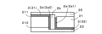
- 2A is an enlarged explanatory diagram for explaining region X shown in FIG. 1
- FIG. 2B is an oblique view showing one embodiment of a through-hole conductor
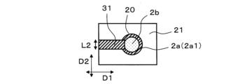
- FIG. 2C is a plan view of region A shown in FIG. 2A as viewed from the direction of arrow A.
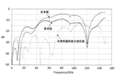
- 13 is data showing a simulation result of electrical characteristics of a conventional wiring board.
- 13 is data showing a simulation result of electrical characteristics of a conventional wiring board.
- the land is positioned so as to surround the opening of the through hole. Therefore, the current (signal) flowing through the wiring conductor located on the surface of the core insulation layer branches to the left and right at the land. As a result, when the branched signals join together, they collide, disrupting the signal flow and causing the signal to accumulate at the land, locally increasing the potential. When a signal accumulates at the land and the potential increases locally, the subsequent signal is reflected, decreasing the signal transmittance. This decrease in signal transmittance is likely to occur in plated through holes (PTH: Plated Through Hole) located only on the inner wall surface of the through hole. Therefore, there is a demand for a wiring board that reduces signal reflection at plated through holes and improves signal transmittance.
- PTH Plated Through Hole
- the wiring board according to the present disclosure has the configuration described in the section on means for solving the above problems, thereby reducing signal reflection in plated through holes and improving signal transmittance.
- FIG. 1 is an explanatory diagram for explaining a wiring board 1 according to an embodiment of the present disclosure.
- the wiring board 1 according to the embodiment includes an insulating layer 2, a conductor layer 3, and a solder resist 4.
- the insulating layer 2 includes a first insulating layer 21, a second insulating layer 22, and a third insulating layer 23.
- the first insulating layer 21 has a first surface 211 and a second surface 212 located on the opposite side to the first surface 211.
- the first insulating layer 21 is not particularly limited as long as it is made of an insulating material. Examples of insulating materials include resins such as epoxy resin, bismaleimide-triazine resin, polyimide resin, and polyphenylene ether resin. Only one type of these resins may be used, or two or more types may be used in combination.
- the first insulating layer 21 corresponds to the insulating layer for the core.
- the thickness of the first insulating layer 21 is not particularly limited.
- the first insulating layer 21 may have a thickness of, for example, 10 ⁇ m or more and 1500 ⁇ m or less.
- the first insulating layer 21 may contain a reinforcing material.
- reinforcing materials include insulating cloth materials such as glass fiber, glass nonwoven fabric, aramid nonwoven fabric, aramid fiber, and polyester fiber. Only one type of reinforcing material may be used, or two or more types may be used in combination.
- the first insulating layer 21 may have inorganic insulating fillers such as silica, barium sulfate, talc, clay, glass, calcium carbonate, and titanium oxide dispersed therein. Only one type of inorganic insulating filler may be used, or two or more types may be used in combination.
- the first surface 211 and the second surface 212 of the first insulating layer 21 are provided with a build-up layer in which conductor layers 3 and insulating layers 2 are alternately stacked. At least two conductor layers 3 and at least one insulating layer 2 are provided in each build-up layer.
- the insulating layer 2 in contact with the first surface 211 corresponds to the second insulating layer 22
- the insulating layer 2 in contact with the second surface 212 corresponds to the third insulating layer 23.
- the insulating layer 2 constituting the build-up layer is not particularly limited as long as it is made of an insulating material.
- insulating materials include resins such as epoxy resin, bismaleimide-triazine resin, polyimide resin, and polyphenylene ether resin. These resins may be used alone or in combination of two or more types.
- the insulating layers 2 constituting the build-up layer may be made of the same resin or different resins.
- the insulating layers 2 and the first insulating layer 21 constituting the build-up layer may be made of the same resin or different resins.
- the thickness of the insulating layer 2 constituting the build-up layer is not particularly limited.
- the insulating layer 2 constituting the build-up layer may have a thickness of, for example, 5 ⁇ m or more and 100 ⁇ m or less.
- the insulating layers 2 constituting the build-up layer may each have the same thickness, or may have different thicknesses.
- the insulating layer 2 constituting the build-up layer may contain a reinforcing material.
- reinforcing materials include insulating cloth materials such as glass fiber, glass nonwoven fabric, aramid nonwoven fabric, aramid fiber, and polyester fiber. Only one type of reinforcing material may be used, or two or more types may be used in combination.
- the insulating layer 2 constituting the build-up layer may have inorganic insulating fillers such as silica, barium sulfate, talc, clay, glass, calcium carbonate, and titanium oxide dispersed therein. Only one type of inorganic insulating filler may be used, or two or more types may be used in combination.
- the conductor layer 3 is not limited as long as it is a conductor such as a metal.
- the conductor layer 3 is formed of a metal such as copper.
- the thickness of the conductor layer 3 is not particularly limited, and is, for example, 1 ⁇ m or more and 70 ⁇ m or less.
- the "first wiring conductor 31" included in the conductor layer 3 is located on the first surface 211 of the first insulating layer 21 and is electrically connected to the through-hole conductor 2a described later.
- the "second wiring conductor 32" included in the conductor layer 3 is located on the second surface 212 of the first insulating layer 21 and is electrically connected to the through-hole conductor 2a described later.
- the conductor layer 3 includes a power supply conductor, a ground conductor, and a signal conductor.
- the first wiring conductor 31 may be a "first signal wiring conductor” and the second wiring conductor 32 may be a "second signal wiring conductor”.
- via-hole conductors 3a are located to electrically connect the upper and lower surfaces of the insulating layer 2.
- the via-hole conductors 3a are located in via holes that are formed to penetrate the insulating layer 2.
- the via-hole conductors 3a are part of the conductor layer 3, and are formed of a metal such as copper.
- a solder resist 4 may be located on the surface of the build-up layer.
- the solder resist 4 is made of a resin, such as an acrylic-modified epoxy resin.
- the solder resist 4 has openings to electrically connect the conductor layer 3 and the electrodes of the elements via solder 5. Examples of the elements include semiconductor integrated circuit elements and optoelectronic elements.
- the through-hole conductor 2a is located in the first insulating layer 21 to electrically connect the top and bottom surfaces of the first insulating layer 21.
- the through-hole conductor 2a is located in a through-hole 20 that penetrates the first insulating layer 21 from the top surface to the bottom surface.
- the through-hole conductor 2a is formed of a metal such as copper.
- the through-hole conductor 2a is electrically connected to the first wiring conductor 31 located on the first surface 211 of the first insulating layer 21 and the second wiring conductor 32 located on the second surface 212 of the first insulating layer 21.
- FIG. 2A is an enlarged explanatory diagram for explaining the region X shown in FIG. 1.
- the through-hole conductor 2a is located only on the inner wall surface of the through-hole 20.
- resin 2b is located in the through-hole 20.
- Resin 2b is located so as to be surrounded by the through-hole conductor 2a.
- Resin 2b is a filling resin that fills the space surrounded by the through-hole conductor 2a.
- resins that can be used include epoxy resin, bismaleimide-triazine resin, polyimide resin, and polyphenylene ether resin. Two or more of these resins may be mixed together.
- the through-hole conductor 2a includes a first portion 2a1, a second portion 2a2, and a third portion 2a3.
- the thickness of the through-hole conductor 2a is set appropriately depending on the diameter of the through-hole 20.
- the thickness of the through-hole conductor 2a may be approximately 1% or more and 30% or less of the radius of the through-hole 20.
- the first portion 2a1 of the through-hole conductor 2a has a first end 2a11 located on the first surface 211 side and a second end 2a12 located on the second surface 212 side in the thickness direction of the first insulating layer 21.
- FIG. 2B is a perspective view showing one embodiment of the through-hole conductor 2a.
- the first portion 2a1 of the through-hole conductor 2a is located around the entire inner wall surface of the through-hole 20.
- FIG. 2C is a plan view of the area A shown in FIG. 2A as viewed from the direction of arrow A.
- At least the first end 2a11 is located closer to the second surface 212 than the first surface 211 in the thickness direction of the first insulating layer 21, as shown in Figures 2A and 2B. In other words, at least the first end 2a11 is not flush with the first surface 211, but is recessed from the first surface 211.
- the second portion 2a2 of the through-hole conductor 2a is connected to a first region that is a part of the first end 2a11 of the first portion 2a1, as shown in Figures 2A and 2B.
- the second portion 2a2 is not located along the entire inner wall surface of the through-hole 20, as shown in Figure 2B.
- the second portion 2a2 is located from the first region to the first surface 211 in the thickness direction of the first insulating layer 21.
- the second portion 2a2 is in contact with the first wiring conductor 31.
- the first wiring conductor 31 is in contact with the end of the second portion 2a2 opposite the first portion 2a1. Because the second portion 2a2 is not positioned along the entire inner wall surface of the through-hole 20, the current (signal) flowing through the first wiring conductor 31 does not branch to the left and right at the through-hole conductor 2a. Therefore, the branched signals do not merge, causing the flow to become turbulent and stagnate, as in the conventional case. As a result, reflection of the subsequent signal is reduced, and the transmittance of the signal is improved.
- the length L1 of the second portion 2a2 is not limited.
- the length L2 of the first wiring conductor 31 in the second direction D2 may be the same as the length L1 of the second portion 2a2.
- the length L2 of the first wiring conductor 31 and the length L1 of the second portion 2a2 are the same is defined not only as being completely the same, but also as being the same within a range of about ⁇ 10%. In other words, if the length L1 is 1, and the length L2 is 0.9 to 1.1, the length L1 and the length L2 are defined as being the same.
- the first wiring conductor 31 may be a first signal wiring conductor.
- one second portion 2a2 is located at the first end 2a11. Multiple second portions 2a2 may be located at the first end 2a11. Multiple first wiring conductors 31 may also be located depending on the number of second portions 2a2.
- the through hole 20 has a first recess 2b1 with the first end 2a11 as its bottom.
- the first recess 2b1 is a recess whose wall surfaces are the resin 2b and the first insulating layer 21, and whose bottom is an area other than the first area of the first end 2a11.
- the shape of the bottom may be, for example, a C-shape in which a part of a ring is cut off in a plan view.
- a part of the second insulating layer 22 is located in the first recess 2b1. This structure reduces peeling of the second insulating layer 22.
- the through-hole conductor 2a includes a third portion 2a3. As shown in FIG. 2A, the third portion 2a3 is connected to a second region that is a part of the second end 2a12 of the first portion 2a1. In other words, unlike the first portion 2a1, the third portion 2a3 is not located along the entire inner wall surface of the through-hole 20. The third portion 2a3 is located from the second region to the second surface 212 in the thickness direction of the first insulating layer 21.
- the third portion 2a3 is in contact with the second wiring conductor 32.
- the second wiring conductor 32 is in contact with the end of the third portion 2a3 opposite the first portion 2a1. Because the third portion 2a3 is not located along the entire inner wall surface of the through-hole 20, the current (signal) flowing through the second wiring conductor 32 does not branch to the left and right at the through-hole conductor 2a. Therefore, the signal transmittance is improved compared to when the third portion 2a3 is not located.
- the length of the third portion 2a3 is not limited.
- the direction in which the second wiring conductor 32 extends from the third portion 2a3 is the third direction (the same direction as the first direction D1) and the direction perpendicular to the third direction is the fourth direction (the same direction as the second direction D2)
- the length of the second wiring conductor 32 in the fourth direction and the length of the third portion 2a3 may be the same.
- the definition of "having the same length" is as described above, and a detailed explanation will be omitted.
- the second wiring conductor 32 may be a second signal wiring conductor.
- the third portion 2a3 may be located at one position at the second end 2a12, or multiple positions may be located. Depending on the number of third portions 2a3, multiple second wiring conductors 32 may also be located.
- a second recess 2b2 is located, with the second end 2a12 as its bottom.
- the second recess 2b2 is a recess whose wall surfaces are the resin 2b and the third insulating layer 23, and whose bottom is an area other than the second area of the second end 2a12.
- the shape of the bottom may be, for example, a C-shape in which a part of a ring is cut off in a plan view.
- a part of the third insulating layer 23 is located in the second recess 2b2. With this structure, peeling of the third insulating layer 23 is reduced.
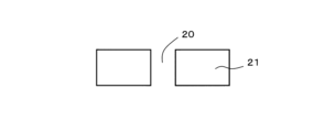
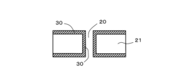
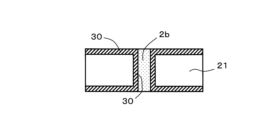
- Figures 3A to 3H are explanatory diagrams for explaining one embodiment of a method for forming the through-hole conductor 2a located in region X shown in Figure 1.
- through holes 20 are formed so as to penetrate the top and bottom surfaces of the first insulating layer 21.
- the size and number of the through holes 20 are set appropriately depending on the size of the wiring board 1 to be finally obtained.
- the through holes 20 are formed using, for example, a drill, a laser, or a blast. If necessary, a desmear process is performed to remove resin residues, etc.
- conductors 30 are formed on the upper and lower surfaces of the first insulating layer 21 and on the inner wall surface of the through hole 20.
- the conductors 30 are formed, for example, by precipitating a metal such as copper by plating such as electrolytic plating.
- a seed layer may be formed on the upper and lower surfaces of the first insulating layer 21 and on the inner wall surface of the formed through hole 20 before electrolytic plating.
- the formation of the seed layer allows metal to be efficiently precipitated by electrolytic plating.
- the seed layer is formed of a metal such as copper by, for example, electroless plating.
- resin 2b is filled into through-hole 20.
- Resin 2b is as described above, and a detailed description is omitted.
- FIG. 3E is a plan view of region B shown in Figure 3D, viewed from the direction of arrow B.
- the resist 6 is, for example, a dry film resist.
- the conductor 30 covered with the resist 6 is protected.
- the resist 6 may be formed to cover not only the conductor 30 to be protected, but also part of the resin 2b. By forming the resist 6 to cover part of the resin 2b, the conductor 30 to be protected is less likely to be eroded during the etching process described below.
- the conductor 30 that is not covered with the resist 6 is removed by an etching process. Not only the conductor 30 formed on the top and bottom surfaces of the first insulating layer 21, but also a part of the conductor 30 formed on the inner wall surface of the through hole 20 is removed. The removed parts correspond to the first recess 2b1 and the second recess 2b2.
- the resist 6 is removed.
- the second insulating layer 22 is formed on the first surface 211 of the first insulating layer 21 so as to cover the first wiring conductor 31.
- the third insulating layer 23 is formed on the second surface 212 of the first insulating layer 21 so as to cover the second wiring conductor 32.
- a portion of the second insulating layer 22 is located in the first recess 2b1, and a portion of the third insulating layer 23 is located in the second recess 2b2.
- Figures 4A to 4D are explanatory diagrams for explaining one embodiment of the method for forming the through-hole conductor 2a located in region Y shown in Figure 1.
- the through-hole conductor 2a located in region X is formed of the first portion 2a1, the second portion 2a2, and the third portion 2a3.
- the through-hole conductor 2a located in region Y is formed of the first portion 2a1 and the second portion 2a2, and does not include the third portion 2a3.
- the through-hole conductor 2a does not need to be formed of the first portion 2a1, the second portion 2a2, and the third portion 2a3, but only needs to be formed of the first portion 2a1 and the second portion 2a2.
- the through-hole conductor 2a formed of the first portion 2a1 and the second portion 2a2 is as shown in Figures 3A to 3C up until the process in which the resin 2b is filled into the through-hole 20, and detailed description will be omitted.
- a resist 6 is formed to remove unnecessary parts of the formed conductor 30.
- the resist 6 is formed to prevent the third portion 2a3 from being formed, i.e., so that a land is formed at one end of the through-hole 20.
- the conductor 30 that is not covered with the resist 6 is removed by an etching process. Not only the conductor 30 formed on the top and bottom surfaces of the first insulating layer 21, but also a part of the conductor 30 formed on the inner wall surface of the through hole 20 is removed. The removed part corresponds to the first recess 2b1. In other words, the second recess 2b2 shown in FIG. 3F is not formed in FIG. 4B.
- a second insulating layer 22 is formed on the first surface 211 of the first insulating layer 21 so as to cover the first wiring conductor 31.
- a third insulating layer 23 is formed on the second surface 212 of the first insulating layer 21 so as to cover the second wiring conductor 32.
- a portion of the second insulating layer 22 is located in the first recess 2b1.
- Figure 5 shows data showing the results of a simulation of the electrical characteristics of the wiring board 1 according to one embodiment of the present disclosure.
- the simulation model uses a first insulating layer 21 (corresponding to the insulating layer for the core, shaped like a square with sides of 6 mm and a thickness of 800 ⁇ m) made of epoxy resin, with a conductor layer 3 of 25 ⁇ m thick copper provided on the first insulating layer 21 (insulating layer for the core).
- the diameter of the through hole 20 is 120 ⁇ m, and the length L1 of the second portion 2a2 of the through hole conductor 2a and the length L2 of the conductor layer 3 (first wiring conductor 31) connected to the second portion 2a2 are both 44 ⁇ m.
- Insertion loss is a measurement of the signal that passes through the output terminal when a signal is input to the input terminal. The higher the dB value, the better the electrical characteristics, and a value of -5 dB or more is usually required at 140 GHz.
- Reflection loss is a measurement of the signal that is reflected back at the input terminal when a signal is input to the input terminal. The smaller the dB value, the better the electrical characteristics, and a value of -15 dB or less is usually required at 140 GHz. As shown in Figure 5, for the wiring board 1 according to one embodiment, the insertion loss at 140 GHz is -5 dB or more, and the reflection loss is -15 dB or less.
- Figures 6 and 7 show data showing the simulation results of the electrical characteristics of the conventional wiring board, together with the simulation results shown in Figure 5 (measured values after application of the present invention).
- Figure 6 shows data showing the insertion loss, which shows that the conventional wiring board is less than -5 dB at 140 GHz and does not meet the required value.
- Figure 7 shows data showing the reflection loss, which shows that the conventional wiring board is greater than -15 dB at 140 GHz and does not meet the required value.
- the measured insertion loss at 140 GHz is -5 dB or more, as shown in FIG. 6, and meets the required value.
- the measured return loss at 140 GHz is -15 dB or less, and meets the required value, as shown in FIG. 7.
- the wiring board 1 according to one embodiment meets the required values for both insertion loss and return loss at 140 GHz, and has improved insertion loss and return loss compared to conventional wiring boards. Therefore, it can be seen that the wiring board according to the present disclosure has excellent electrical properties.
- the wiring board according to the present disclosure includes a first insulating layer having a first surface and a second surface located on the opposite side to the first surface, a through hole penetrating the first insulating layer from the first surface to the second surface, a through hole conductor located on the inner wall surface of the through hole, a first wiring conductor located on the first surface and electrically connected to the through hole conductor, and a second wiring conductor located on the second surface and electrically connected to the through hole conductor.
- the through hole conductor includes a first portion located around the entire inner wall surface and a second portion connecting the first portion and the first wiring conductor.
- the first portion has a first end portion located on the first surface side and a second end portion located on the second surface side in the thickness direction of the first insulating layer. At least the first end portion is located closer to the second surface than the first surface in the thickness direction.
- the second portion is connected to a first region that is a part of the first end portion, and is located from the first region to the first surface in the thickness direction.
- the through-hole conductor further includes a third portion connecting the first portion and the second wiring conductor.
- the second end portion is located closer to the first surface than the second surface in the thickness direction.
- the third portion is connected to a second region of a part of the second end portion and is located from the second region to the second surface in the thickness direction.
- the first wiring conductor includes a first signal wiring conductor located on the first surface
- the second wiring conductor includes a second signal wiring conductor located on the second surface
- the first signal wiring conductor is connected to the second portion
- the second signal wiring conductor is connected to the third portion.
- a direction in which the first signal wiring conductor extends from the second portion is defined as a first direction and a direction perpendicular to the first direction is defined as a second direction
- a length of the first signal wiring conductor in the second direction is equal to a length of the second portion
- a direction in which the second signal wiring conductor extends from the third portion is defined as a third direction and a direction perpendicular to the third direction is defined as a fourth direction
- a length of the second signal wiring conductor in the fourth direction is equal to a length of the third portion.
- a portion of the second insulating layer is located in a first recess having walls formed of the resin and the first insulating layer and a bottom formed of an area other than the first area of the first end.
- a portion of the third insulating layer is located in a second recess having wall surfaces of the resin and the first insulating layer and a bottom surface of an area other than the second region of the second end.
Landscapes
- Engineering & Computer Science (AREA)
- Microelectronics & Electronic Packaging (AREA)
- Manufacturing & Machinery (AREA)
- Structure Of Printed Boards (AREA)
- Printing Elements For Providing Electric Connections Between Printed Circuits (AREA)
Abstract
La présente invention concerne une première couche isolante (21) ayant une première surface (211) et une seconde surface (212) positionnée sur le côté opposé à la première surface, un trou traversant (20) pénétrant dans la première couche isolante de la première surface à la seconde surface, un conducteur de trou traversant (2a) positionné sur la surface de paroi interne du trou traversant, un premier conducteur de câblage (31) positionné sur la première surface et connecté électriquement au conducteur de trou traversant, et un second conducteur de câblage (32) positionné sur la seconde surface et connecté électriquement au conducteur de trou traversant. Le conducteur de trou traversant comprend une première partie (2a1) positionnée sur toute la circonférence de la surface de paroi interne, et une seconde partie (2a2) reliant la première partie et le premier conducteur de câblage. La première partie a une première partie d'extrémité située sur le premier côté de surface et une seconde partie d'extrémité située sur le second côté de surface dans la direction de l'épaisseur de la première couche isolante. La première partie d'extrémité est située plus près du côté de la seconde surface que la première surface dans la direction de l'épaisseur. La seconde partie est reliée à une première région constituant une partie de la première partie d'extrémité, et est positionnée de la première région à la première surface dans la direction de l'épaisseur.
Applications Claiming Priority (2)
| Application Number | Priority Date | Filing Date | Title |
|---|---|---|---|
| JP2023-106911 | 2023-06-29 | ||
| JP2023106911 | 2023-06-29 |
Publications (1)
| Publication Number | Publication Date |
|---|---|
| WO2025004902A1 true WO2025004902A1 (fr) | 2025-01-02 |
Family
ID=93939031
Family Applications (1)
| Application Number | Title | Priority Date | Filing Date |
|---|---|---|---|
| PCT/JP2024/022016 Ceased WO2025004902A1 (fr) | 2023-06-29 | 2024-06-18 | Carte de câblage |
Country Status (2)
| Country | Link |
|---|---|
| TW (1) | TW202508377A (fr) |
| WO (1) | WO2025004902A1 (fr) |
Citations (6)
| Publication number | Priority date | Publication date | Assignee | Title |
|---|---|---|---|---|
| JPH0637416A (ja) * | 1992-07-14 | 1994-02-10 | Fujitsu Ltd | プリント配線板 |
| JPH06338687A (ja) * | 1993-05-31 | 1994-12-06 | Nec Corp | 多層印刷配線板およびその製造方法 |
| JPH1154869A (ja) * | 1997-08-07 | 1999-02-26 | Hitachi Ltd | 実装基板とそれを用いた電子装置 |
| JP2001210953A (ja) * | 2000-01-27 | 2001-08-03 | Ngk Spark Plug Co Ltd | 配線基板及び配線基板の製造方法 |
| JP2005175189A (ja) * | 2003-12-11 | 2005-06-30 | Fuji Xerox Co Ltd | プリント配線基板 |
| WO2019082845A1 (fr) * | 2017-10-25 | 2019-05-02 | 株式会社Soken | Ligne de transmission à haute fréquence |
-
2024
- 2024-06-18 WO PCT/JP2024/022016 patent/WO2025004902A1/fr not_active Ceased
- 2024-06-25 TW TW113123589A patent/TW202508377A/zh unknown
Patent Citations (6)
| Publication number | Priority date | Publication date | Assignee | Title |
|---|---|---|---|---|
| JPH0637416A (ja) * | 1992-07-14 | 1994-02-10 | Fujitsu Ltd | プリント配線板 |
| JPH06338687A (ja) * | 1993-05-31 | 1994-12-06 | Nec Corp | 多層印刷配線板およびその製造方法 |
| JPH1154869A (ja) * | 1997-08-07 | 1999-02-26 | Hitachi Ltd | 実装基板とそれを用いた電子装置 |
| JP2001210953A (ja) * | 2000-01-27 | 2001-08-03 | Ngk Spark Plug Co Ltd | 配線基板及び配線基板の製造方法 |
| JP2005175189A (ja) * | 2003-12-11 | 2005-06-30 | Fuji Xerox Co Ltd | プリント配線基板 |
| WO2019082845A1 (fr) * | 2017-10-25 | 2019-05-02 | 株式会社Soken | Ligne de transmission à haute fréquence |
Also Published As
| Publication number | Publication date |
|---|---|
| TW202508377A (zh) | 2025-02-16 |
Similar Documents
| Publication | Publication Date | Title |
|---|---|---|
| KR100702554B1 (ko) | 다층 전자 장치 캐리어의 개량된 적층 비아 구조 | |
| US6996903B2 (en) | Formation of multisegmented plated through holes | |
| JP7155261B2 (ja) | 無線周波数回路におけるアディティブ製造技術(amt)ファラデー境界 | |
| US6072375A (en) | Waveguide with edge grounding | |
| JP2002353588A (ja) | 配線基板及び配線基板の製造方法 | |
| US20140034363A1 (en) | Multi-layer transmission lines | |
| US4646436A (en) | Shielded interconnection boards | |
| JP7097139B2 (ja) | 配線基板 | |
| EP0668713B1 (fr) | Procédé de fabrication d'un panneau à micro-ondes multicouche, et panneau obtenu par ce procédé | |
| US20100308941A1 (en) | High-frequency line structure on resin substrate and method of manufacturing the same | |
| TWI815528B (zh) | 電路板結構 | |
| WO2025004902A1 (fr) | Carte de câblage | |
| US7290333B2 (en) | Manufacturing method of a multilayer printed wiring board | |
| US7196906B1 (en) | Circuit board having segments with different signal speed characteristics | |
| JP7397718B2 (ja) | 印刷配線板及び印刷配線板の製造方法 | |
| US6441319B1 (en) | Inserted components for via connection of signal tracks to achieve continuous impedance matching in multi-layer substrate | |
| WO2022176853A1 (fr) | Carte de circuit imprimé | |
| US6459347B1 (en) | Method for vertical connection of conductors in a device in the microwave range | |
| WO2025070312A1 (fr) | Carte de câblage et structure de montage l'utilisant | |
| US20230292431A1 (en) | Shielded signal vias in printed circuit boards for high-frequency and broadband signals | |
| WO2025070043A1 (fr) | Carte de câblage et structure de boîtier la comprenant | |
| WO2025089165A1 (fr) | Carte de câblage et structure de montage l'utilisant | |
| WO2026070212A1 (fr) | Carte de câblage et structure de montage | |
| US20250168970A1 (en) | Wiring board | |
| WO2026028759A1 (fr) | Carte de câblage et structure de montage |
Legal Events
| Date | Code | Title | Description |
|---|---|---|---|
| 121 | Ep: the epo has been informed by wipo that ep was designated in this application |
Ref document number: 24831764 Country of ref document: EP Kind code of ref document: A1 |
|
| NENP | Non-entry into the national phase |
Ref country code: DE |