WO2025018351A1 - Source de lumière, dispositif de mesure, procédé de fabrication de source de lumière et procédé de fabrication de dispositif de mesure - Google Patents
Source de lumière, dispositif de mesure, procédé de fabrication de source de lumière et procédé de fabrication de dispositif de mesure Download PDFInfo
- Publication number
- WO2025018351A1 WO2025018351A1 PCT/JP2024/025538 JP2024025538W WO2025018351A1 WO 2025018351 A1 WO2025018351 A1 WO 2025018351A1 JP 2024025538 W JP2024025538 W JP 2024025538W WO 2025018351 A1 WO2025018351 A1 WO 2025018351A1
- Authority
- WO
- WIPO (PCT)
- Prior art keywords
- light
- emitting chip
- light source
- semiconductor laser
- conductive pattern
- Prior art date
- Legal status (The legal status is an assumption and is not a legal conclusion. Google has not performed a legal analysis and makes no representation as to the accuracy of the status listed.)
- Ceased
Links
Images





Classifications
-
- G—PHYSICS
- G01—MEASURING; TESTING
- G01S—RADIO DIRECTION-FINDING; RADIO NAVIGATION; DETERMINING DISTANCE OR VELOCITY BY USE OF RADIO WAVES; LOCATING OR PRESENCE-DETECTING BY USE OF THE REFLECTION OR RERADIATION OF RADIO WAVES; ANALOGOUS ARRANGEMENTS USING OTHER WAVES
- G01S17/00—Systems using the reflection or reradiation of electromagnetic waves other than radio waves, e.g. lidar systems
- G01S17/88—Lidar systems specially adapted for specific applications
- G01S17/93—Lidar systems specially adapted for specific applications for anti-collision purposes
- G01S17/931—Lidar systems specially adapted for specific applications for anti-collision purposes of land vehicles
-
- G—PHYSICS
- G01—MEASURING; TESTING
- G01S—RADIO DIRECTION-FINDING; RADIO NAVIGATION; DETERMINING DISTANCE OR VELOCITY BY USE OF RADIO WAVES; LOCATING OR PRESENCE-DETECTING BY USE OF THE REFLECTION OR RERADIATION OF RADIO WAVES; ANALOGOUS ARRANGEMENTS USING OTHER WAVES
- G01S7/00—Details of systems according to groups G01S13/00, G01S15/00, G01S17/00
- G01S7/48—Details of systems according to groups G01S13/00, G01S15/00, G01S17/00 of systems according to group G01S17/00
- G01S7/481—Constructional features, e.g. arrangements of optical elements
-
- G—PHYSICS
- G01—MEASURING; TESTING
- G01S—RADIO DIRECTION-FINDING; RADIO NAVIGATION; DETERMINING DISTANCE OR VELOCITY BY USE OF RADIO WAVES; LOCATING OR PRESENCE-DETECTING BY USE OF THE REFLECTION OR RERADIATION OF RADIO WAVES; ANALOGOUS ARRANGEMENTS USING OTHER WAVES
- G01S7/00—Details of systems according to groups G01S13/00, G01S15/00, G01S17/00
- G01S7/48—Details of systems according to groups G01S13/00, G01S15/00, G01S17/00 of systems according to group G01S17/00
- G01S7/483—Details of pulse systems
- G01S7/484—Transmitters
-
- H—ELECTRICITY
- H01—ELECTRIC ELEMENTS
- H01S—DEVICES USING THE PROCESS OF LIGHT AMPLIFICATION BY STIMULATED EMISSION OF RADIATION [LASER] TO AMPLIFY OR GENERATE LIGHT; DEVICES USING STIMULATED EMISSION OF ELECTROMAGNETIC RADIATION IN WAVE RANGES OTHER THAN OPTICAL
- H01S5/00—Semiconductor lasers
- H01S5/02—Structural details or components not essential to laser action
- H01S5/022—Mountings; Housings
- H01S5/0233—Mounting configuration of laser chips
- H01S5/02345—Wire-bonding
-
- H—ELECTRICITY
- H01—ELECTRIC ELEMENTS
- H01S—DEVICES USING THE PROCESS OF LIGHT AMPLIFICATION BY STIMULATED EMISSION OF RADIATION [LASER] TO AMPLIFY OR GENERATE LIGHT; DEVICES USING STIMULATED EMISSION OF ELECTROMAGNETIC RADIATION IN WAVE RANGES OTHER THAN OPTICAL
- H01S5/00—Semiconductor lasers
- H01S5/02—Structural details or components not essential to laser action
- H01S5/022—Mountings; Housings
- H01S5/0235—Method for mounting laser chips
- H01S5/02355—Fixing laser chips on mounts
- H01S5/0236—Fixing laser chips on mounts using an adhesive
-
- H—ELECTRICITY
- H01—ELECTRIC ELEMENTS
- H01S—DEVICES USING THE PROCESS OF LIGHT AMPLIFICATION BY STIMULATED EMISSION OF RADIATION [LASER] TO AMPLIFY OR GENERATE LIGHT; DEVICES USING STIMULATED EMISSION OF ELECTROMAGNETIC RADIATION IN WAVE RANGES OTHER THAN OPTICAL
- H01S5/00—Semiconductor lasers
- H01S5/10—Construction or shape of the optical resonator, e.g. extended or external cavity, coupled cavities, bent-guide, varying width, thickness or composition of the active region
- H01S5/18—Surface-emitting [SE] lasers, e.g. having both horizontal and vertical cavities
- H01S5/183—Surface-emitting [SE] lasers, e.g. having both horizontal and vertical cavities having only vertical cavities, e.g. vertical cavity surface-emitting lasers [VCSEL]
Definitions
- the technology disclosed in this specification relates to a light source, a measurement device, a method for manufacturing a light source, and a method for manufacturing a measurement device.
- LiDAR Light Detection and Ranging
- a projector that projects (irradiates) laser light onto the measurement target
- a receiver that receives the reflected light that reflects the laser light off the measurement target.
- LiDAR outputs information about the measurement target by measuring the distance to the measurement target based on the difference between the timing when the projector emits the laser light and the timing when the receiver receives the reflected light.
- the floodlight comprises a light source and a projection lens through which the light emitted by the light source passes (see, for example, Patent Document 1).
- the light projector also has a semiconductor laser that emits laser light.
- the light receiver has a filter that passes laser light in a predetermined passband that is output from the light projector and reflected by the object to be measured, and a light receiving element that receives the laser light that has passed through the filter (see, for example, Patent Document 1).
- the inventors have considered using a light source including a light-emitting chip on which a surface-emitting element is arranged as a light source to be provided in a floodlight.
- This light source includes a light-emitting chip, a substrate, a conductive joint, and a wire.
- the light-emitting chip has a first surface electrically connected to the cathode of the surface-emitting element, and a second surface electrically connected to the anode of the surface-emitting element.
- a first conductive pattern and a second conductive pattern are formed on the substrate.
- the joint joins the first surface of the light-emitting chip to the first conductive pattern.
- the wire electrically connects the second surface of the light-emitting chip to the second conductive pattern.
- the cathode of the surface-emitting element may short-circuit to a conductive member, such as a wire or the anode of the surface-emitting element, via a conductive joint.
- This specification discloses a technology that can solve the problems mentioned above.
- a specified wavelength band is indicated on the spec sheet of a semiconductor laser.
- the specified wavelength band is a range of variation that is assumed in advance for the wavelength of the laser light emitted by the semiconductor laser.
- the specified wavelength band is specified, for example, based on the manufacturing variation of the semiconductor laser. In conventional measuring devices, it is assumed that the wavelength of the laser light from the semiconductor laser varies within the specified wavelength band, and the pass band of the filter of the optical receiver is set to a band that includes the specified wavelength band.
- the actual wavelength band of the laser light emitted by the semiconductor laser installed in the measuring device is only a part of the specified wavelength band.
- the passband of the filter is set to a bandwidth that is much wider than the wavelength band required for actual measurement.
- the light receiving element is prone to receiving not only the laser light emitted by the semiconductor laser, but also noise (external light such as sunlight that has a different wavelength from the semiconductor laser), which may result in a decrease in the measurement accuracy of the measuring device (for example, the measurable distance may become shorter).
- This specification discloses a technology that can solve the problems mentioned above.
- a light source includes a light emitting chip on which a surface light emitting element is arranged, the light emitting chip having a first surface electrically connected to the cathode of the surface light emitting element and a second surface electrically connected to the anode of the surface light emitting element, a substrate on which a first conductive pattern and a second conductive pattern are formed, a conductive joint that joins the first surface of the light emitting chip to the first conductive pattern, and a wire that electrically connects the second surface of the light emitting chip to the second conductive pattern, and includes a non-conductive protective part that is arranged on the outer periphery of the joint and covers at least a portion of the outer periphery of the joint.
- this light source can prevent the cathode of the surface-emitting element from shorting out to a conductive member, such as the anode of the surface-emitting element, via the joint.
- a connection portion to which the wire is electrically connected may be provided on the peripheral portion of the second surface of the light-emitting chip, and the protective portion may be configured to cover the outer peripheral surface of the joint on the side of the connection portion.
- the protective portion may be configured to cover the entire outer periphery of the joint.
- the protective part when viewed in a direction perpendicular to the light-emitting chip, at least a part of the outer peripheral surface of the joint is located inside the outer edge of the light-emitting chip, and the protective part may have a support part that is sandwiched between the light-emitting chip and the substrate.
- the support part of the protective part is interposed in the gap formed between the light-emitting chip and the substrate due to the absence of the joint. Therefore, according to this light source, it is possible to suppress damage to the light-emitting chip due to the application of a load to the light-emitting chip, for example, compared to a configuration in which a support part is not interposed.
- the protective portion may be in contact with the outer peripheral surface of the joint, and the area of the exposed surface of the protective portion may be larger than the contact area between the protective portion and the joint. According to this light source, the protective portion is in contact with the outer peripheral surface of the joint that functions as a conductive path. Also, the area of the exposed surface of the protective portion is larger than the contact area between the protective portion and the joint. Therefore, heat generated at the joint can be effectively released via the protective portion.
- the measurement device may include a light projector having a light source according to any one of (1) to (5) above, and a light receiver that receives the light output from the light projector and reflected by the object to be measured.
- a method for manufacturing a light source includes a light emitting chip on which a surface light emitting element is arranged, the light emitting chip having a first surface electrically connected to the cathode of the surface light emitting element and a second surface electrically connected to the anode of the surface light emitting element, and a substrate on which a first conductive pattern and a second conductive pattern are formed, the method including the steps of: applying a conductive first bonding material between the first surface of the light emitting chip and the first conductive pattern of the substrate, and applying a non-conductive second bonding material to at least a part of the periphery of the first bonding material; electrically connecting the second surface of the light emitting chip and the second conductive pattern by a wire; and hardening the first bonding material and the second bonding material to form a conductive bonding portion formed between the first surface of the light emitting chip and the substrate, and a protective portion covering at least a part of the outer circumferential surface of
- a light source is a light source including a light-emitting chip on which a surface-emitting element is arranged, the light-emitting chip having a first surface electrically connected to the cathode of the surface-emitting element and a second surface electrically connected to the anode of the surface-emitting element, a substrate on which a first conductive pattern and a second conductive pattern are formed, a conductive joint that joins the first surface of the light-emitting chip to the first conductive pattern, and a wire that electrically connects the second surface of the light-emitting chip to the second conductive pattern, and when viewed in a first direction perpendicular to the light-emitting chip, at least a part of the outer peripheral surface of the joint is located inside the outer edge of the light-emitting chip, and the connection part between the wire and the second surface is located inside the outer peripheral surface of the joint.
- this light source for example, compared to a configuration in which the joint part between the wire and the light-emitting chip is located outside the outer peripheral surface of the joint part, it is possible to suppress damage to the light-emitting chip due to, for example, application of a load to the connection part of the light-emitting chip.
- the periphery of the light-emitting region of the light-emitting chip when viewed in the first direction, may be located inside the outer peripheral surface of the joint, and the inclination angle ⁇ of a virtual plane passing through the ridge of the light-emitting region and the ridge of the outer peripheral surface of the joint with respect to the first direction may be 45 degrees or more.
- a measurement device includes a projector having a semiconductor laser that emits laser light, a filter that passes a specific passband of the laser light output from the projector and reflected by a measurement target, and a receiver having a light receiving element that receives the laser light that has passed through the filter, and the specific passband of the filter is a part of a specified wavelength band that is specified based on manufacturing variations of the semiconductor laser.
- the semiconductor laser includes a first semiconductor laser and a second semiconductor laser
- the filter includes a first filter that passes the laser light emitted by the first semiconductor laser and a second filter that passes the laser light emitted by the second semiconductor laser
- the first semiconductor laser and the second semiconductor laser have the same specified wavelength band
- the first filter and the second filter have different specific pass bands.
- the bandwidth of the specific passband may be configured to be 1/2 or less of the bandwidth of the specified wavelength band.
- a method for manufacturing a measuring device includes a projector having a semiconductor laser that emits laser light, a filter that passes a laser light in a specific passband among the laser light output from the projector and reflected by a measurement target, and a receiver having a light receiving element that receives the laser light that has passed through the filter, and includes a step of determining to which of a plurality of wavelength classes a selected semiconductor laser selected from a plurality of semiconductor lasers belongs by dividing a specified wavelength band that is specified based on manufacturing variations of the semiconductor lasers, and a step of arranging the filter having a specific passband corresponding to the wavelength class to which the selected semiconductor laser belongs in the receiver. According to this manufacturing method, a measuring device in which the influence of noise is more effectively suppressed can be efficiently manufactured.
- the technology disclosed in this specification can be realized in various forms, such as a light source, a measuring device equipped with the light source, a method for manufacturing a light source, a method for selecting filters, a method for manufacturing a measuring device, etc.
- FIG. 1 is a block diagram illustrating a schematic configuration of a measurement device 110 according to a first embodiment.
- 2 is an explanatory diagram showing the top surface configuration of a light source 122.
- FIG. 3 is an explanatory diagram showing a cross-sectional configuration of the light source 122 at the position of III-III in FIG. 2.
- 4 is a flowchart showing a part of a manufacturing process of the light source 122.
- 13 is an explanatory diagram showing a top view configuration of a light source 122a in the second embodiment.
- FIG. 6 is an explanatory diagram showing a cross-sectional configuration of the light source 122 taken along the line VI-VI in FIG. 5.
- FIG. 2 is a block diagram illustrating a schematic configuration of a measurement device 210 according to an embodiment.
- FIG. 1 is an explanatory diagram showing a prescribed wavelength band B of a semiconductor laser 223.
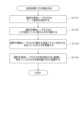
- FIG. 4 is a flowchart showing a part of a manufacturing process of the measuring device 210.
- FIG. 13 is an explanatory diagram showing classification of the prescribed wavelength band B.
- 1 is an explanatory diagram showing a specific pass band H1 for a first wavelength class f1;
- FIG. 11 is an explanatory diagram showing a specific pass band H2 for a second wavelength class f2.
- A. First embodiment: A-1. Configuration of the measuring device 110: 1 is a block diagram showing a schematic configuration of a measuring device 110 in the first embodiment.
- the measuring device 110 includes a projector 120 that irradiates an emitted light L1 (e.g., a light beam (laser light)) onto a measuring object W, and a receiver 130 that receives a reflected light L2 (return light) that is reflected by the measuring object W and returns from the emitted light L1, and functions as a flash LiDAR.
- L1 e.g., a light beam (laser light)
- L2 return light
- the measuring device 110 measures the difference between the timing at which the projector 120 emits the emitted light L1 and the timing at which the receiver 130 receives the reflected light L2 (time of flight of the laser light, hereinafter referred to as "TOF" (Time of Flight)) to obtain information about the measuring object W.
- TOF Time of Flight
- the measuring device 110 is mounted, for example, on a vehicle (not shown) equipped with AD or ADAS.
- the measuring device 110 assists in the detection of objects such as people and other vehicles while the vehicle is traveling, and provides various information to other devices and users that is useful for ensuring the safety of the driver of the vehicle and those around the vehicle, and for reducing damage to surrounding objects while the vehicle is being driven.
- the floodlight 120 has a light source 122, a floodlight optical system 124, a floodlight control device 126, and a current source 128.
- the light source 122 includes a light emitting source having one or more light emitting elements (not shown), or one or more light emitting element arrays (e.g., light emitting elements arranged in a line (one-dimensional) or surface (two-dimensional)). As described below, in this embodiment, the light emitting elements are surface light emitting elements 1110. The configuration of the light source 122 will be described later.
- the current source 128 supplies a current corresponding to a control signal input from the light projection control device 126 to the light emitting element that constitutes the light source 122.
- the current source 128 supplies, for example, a periodic square wave current to the light emitting element for turning on and off the current flowing through the light emitting element.
- the light-projection control device 126 generates a control signal for controlling the current source 128 and inputs it to the current source 128, thereby controlling the current (drive current) supplied from the current source 128 to the light-emitting element.
- the light-projection control device 126 inputs a signal indicating the timing at which the light-emitting element emits light (the timing at which the light-emitting element emits light; hereinafter referred to as "light-projection timing") to the TOF measurement device 40.
- the light-projection control device 126 periodically and repeatedly controls the on-off of the current flowing through the light-emitting element, for example, to cause the light-emitting element to emit light periodically and repeatedly.
- the projection optical system 124 adjusts the light distribution of the emitted light L1, for example, by applying optical effects (such as refraction, scattering, and diffraction) to the light emitted by the light source 122.
- the projection optical system 124 is configured using optical components, such as various lenses, such as collimating lenses, and reflectors (mirrors).
- the receiver 130 has a light receiving section 132 and a light receiving optical system 134.
- the light receiving optical system 134 collects reflected light L2, which is light L1 emitted from the projector 120 and reflected by the measurement target W or the like, on the light receiving unit 132.
- the light receiving optical system 134 is configured using optical components such as various lenses, such as a collecting lens, various filters, such as a wavelength filter, and a reflector (mirror).
- the light receiving unit 132 is a receiving light source having one or more light receiving elements (not shown), or one or more light receiving element arrays (e.g., light receiving elements arranged linearly (one-dimensionally) or planarly (two-dimensionally)).
- the light receiving elements are, for example, photodiodes, SPADs (Single Photon Avalanche Diodes), balanced photodetectors, etc.
- the light receiving unit 132 photoelectrically converts the reflected light L2 incident from the light receiving optical system 134 to generate a current (hereinafter referred to as the "receiving current") according to the intensity of the reflected light L2.
- the light receiving unit 132 inputs a signal indicating the timing (hereinafter referred to as the "receiving timing") at which the light receiving elements constituting the light receiving unit 132 receive the reflected light L2, and the receiving current generated by the light receiving elements, to the TOF measurement device 40.
- the measuring device 110 further includes a TOF measuring device 40, a controller 42, and a communication I/F (Interface) 50.
- the TOF measuring device 40 calculates the TOF based on a signal indicating the timing of light projection input from the light projection control device 126 and a signal indicating the timing of light reception input from the light receiving unit 132.
- the TOF measuring device 40 has, for example, a time measurement IC (integrated circuit) equipped with a TDC (time to digital converter) circuit.
- the TOF measuring device 40 inputs the calculated TOF and the light receiving current input from the light receiving unit 132 to the controller 42.
- the controller 42 has a processor (CPU (Central Processing Unit), MPU (Micro Processing Unit), ASIC (Application Specific Integrated Circuit), FPGA (Field Programmable Gate Array), DSP (Digital Signal Processor), etc.).
- the controller 42 generates information used for various measurements such as detection and ranging of the measurement target W based on the received light current and TOF input from the TOF measurement device 40.
- the information is, for example, a histogram used in time-correlated single photon counting, the distance to each point of the measurement target W, a point cloud (point cloud information), etc.
- the controller 42 also controls the light projection control device 126 and the light receiving unit 132.
- the controller 42 controls the light projection timing and light receiving timing described above, for example, by controlling the light projection control device 126 and the light receiving unit 132 so that the processing for generating the histogram is accelerated or optimized.
- the information generated by the controller 42 is provided (transmitted) to a device that uses the information (hereinafter referred to as "various use devices 60") via the communication I/F 50.
- the various utilization devices 60 perform, for example, the creation of environmental maps using point clouds, self-location estimation (SLAM (Simultaneous Localization and Mapping)) using scan matching algorithms (NDT (Normal Distributions Transform), ICP (Iterative Closest Point), etc.).
- SAM Simultaneous Localization and Mapping
- NDT Normal Distributions Transform
- ICP Iterative Closest Point
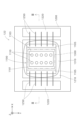
- FIG. 2 is an explanatory diagram showing the top surface configuration of the light source 122
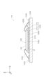
- Fig. 3 is an explanatory diagram showing the cross-sectional configuration of the light source 122 at the position III-III in Fig. 2.
- Figs. 2 and 3 show mutually orthogonal XYZ axes for specifying directions.
- the positive direction of the Z axis is referred to as the upward direction
- the negative direction of the Z axis is referred to as the downward direction
- the positive direction of the X axis is referred to as the rightward direction
- the negative direction of the X axis is referred to as the leftward direction
- the positive direction of the Y axis is referred to as the forward direction
- the negative direction of the Y axis is referred to as the backward direction.
- the light source 122 has a light-emitting chip 1100, a substrate 1200, a conductive joint 1300, and a wire 1250.
- the light-emitting chip 1100 is a surface-emitting element array in which multiple surface-emitting elements 1110 are two-dimensionally arranged on a substrate (semiconductor substrate, ceramic substrate, etc.).
- the surface-emitting element 1110 is a surface-emitting type laser light-emitting element, for example a VCSEL (Vertical Cavity Surface Emitting Laser).
- the light-emitting chip 1100 is a VCSEL array in which multiple VCSELs are arranged.
- the upper surface 1101 of the light-emitting chip 1100 includes a light-emitting region 1103 and a pair of connection regions 1105.
- the upper surface 1101 is an example of a second surface.
- the light-emitting region 1103 is an area in which a plurality of surface-emitting elements 1110 are arranged, and is an area in which light is emitted by the plurality of surface-emitting elements 1110.
- the light-emitting region 1103 is located in the center of the upper surface 1101 in the left-right direction.
- the pair of connection regions 1105 are arranged at both ends of the upper surface 1101 in the left-right direction. Each connection region 1105 is electrically connected to the anodes of the plurality of surface-emitting elements 1110.
- the lower surface 1102 of the light-emitting chip 1100 is electrically connected to the cathodes of the plurality of surface-emitting elements 1110.
- the lower surface 1102 is an example of a first surface.
- a first conductive pattern 1210 and a pair of second conductive patterns 1220 are formed on the substrate 1200.
- the first conductive pattern 1210 is disposed in the center of the substrate 1200 in the left-right direction.
- the pair of second conductive patterns 1220 are disposed at both ends of the substrate 1200 in the left-right direction.
- the joint 1300 is a conductive joint and is made of a conductive material.
- the conductive material may be, for example, a metal (sintered silver, gold-tin (Au-Sn) solder, tin-silver-copper (Sn-Ag-Cu) solder, etc.) or a resin containing a metal (for example, silver) filler.
- the joint 1300 joins the light-emitting chip 1100 and the first conductive pattern 1210 of the substrate 1200, and electrically connects the lower surface 1102 of the light-emitting chip 1100 and the first conductive pattern 1210. Specifically, the upper surface of the joint 1300 is joined in surface contact with the lower surface 1102 of the light-emitting chip 1100. The lower surface of the joint 1300 is joined in surface contact with the upper surface of the first conductive pattern 1210. As a result, the cathodes of the multiple surface-emitting elements 1110 are electrically connected to the first conductive pattern 1210 via the joint 1300.
- the wire 1250 electrically connects the connection area 1105 of the light-emitting chip 1100 and the second conductive pattern 1220 on the substrate 1200. One end of the wire 1250 is joined to the connection area 1105 of the light-emitting chip 1100, and the other end of the wire 1250 is joined to the second conductive pattern 1220.
- the left connection area 1105 and the left second conductive pattern 1220 are electrically connected by multiple wires 1250 arranged at intervals in the front-rear direction.
- the right connection area 1105 and the right second conductive pattern 1220 are electrically connected by multiple wires 1250 arranged at intervals in the front-rear direction.
- the wires 1250 are made of, for example, gold.
- the light source 122 has a configuration for suppressing the cathode of the surface light emitting element 1110 from being short-circuited to the conductive member via the joint 1300.
- the conductive member is, for example, the wire 1250, the second conductive pattern 1220, or another conductive member located around the light emitting chip 1100.
- the light source 122 has a protective section 1310.
- the protective section 1310 is a joint having non-conductivity, and is formed of a non-conductive material.
- the non-conductive material is, for example, a resin.
- the non-conductive material may also be a mixed material in which a filler made of a material having a higher thermal conductivity than resin (for example, a ceramic material such as aluminum oxide (Al 2 O 3 ) or aluminum nitride (AlN)) is mixed into resin in order to enhance heat dissipation.
- the protective portion 1310 covers the entire outer surface S1 of the joint portion 1300. In other words, the entire outer surface S1 of the joint portion 1300 is not exposed to the outside.
- the protective portion 1310 has a support portion 1312 and a protrusion 1314.
- the support portion 1312 is a portion of the protective portion 1310 that is sandwiched between the light emitting chip 1100 and the first conductive pattern 1210 (substrate 1200). Specifically, in this embodiment, when viewed in the vertical direction, the contour line of the joint portion 1300 is located inside the contour line of the light emitting chip 1100 over the entire circumference (see FIG. 2). Therefore, the peripheral portion of the lower surface 1102 of the light emitting chip 1100 is separated from the first conductive pattern 1210 in the vertical direction.
- the support portion 1312 of the protective portion 1310 is disposed in the gap between the peripheral portion of the lower surface 1102 of the light emitting chip 1100 and the first conductive pattern 1210.
- the upper surface of the support portion 1312 is in contact with the peripheral portion of the lower surface 1102 of the light emitting chip 1100, and the lower surface of the support portion 1312 is in contact with the first conductive pattern 1210. In this way, the support portion 1312 supports the peripheral portion of the lower surface 1102 of the light-emitting chip 1100.
- the support portion 1312 is disposed around the entire circumference of the joint portion 1300.
- the support portion 1312 is in contact with the outer peripheral surface S1 of the joint portion 1300 around the entire circumference.
- the up-down view is an example of a view in a direction perpendicular to the light-emitting chip 1100.
- the direction perpendicular to the light-emitting chip 1100 refers to a direction perpendicular to the light-emitting surface of the light-emitting chip 1100.
- the protruding portion 1314 is a portion of the protective portion 1310 that protrudes outward beyond the light emitting chip 1100 when viewed in the up-down direction.
- the area of the exposed surface S2 of the protruding portion 1314 is larger than the contact area (area of the outer peripheral surface S1) between the protective portion 1310 (support portion 1312) and the joint portion 1300.
- the protruding portion 1314 covers the entire outer peripheral surface S1 of the light emitting chip 1100. Therefore, the peripheral portion of the light emitting chip 1100 is protected by the protruding portion 1314.
- the exposed surface S2 of the protruding portion 1314 is a tapered surface that is inclined so as to widen toward the outer periphery as it approaches the substrate 1200. In this way, the exposed surface S2 of the protruding portion 1314 is secured widely, and therefore the heat dissipation by the protective portion 1310 is high.
- FIG. 4 is a flow chart showing a part of the manufacturing process of the light source 122. As shown in Fig. 4, a substrate 1200 on which a first conductive pattern 1210 and a second conductive pattern 1220 are formed is prepared (S1110).
- a first bonding material is applied between the lower surface 1102 of the light-emitting chip 1100 and the first conductive pattern 1210 of the substrate 1200, and a second bonding material is applied around the first bonding material (S1120).
- the first bonding material is made of a bonding material having electrical conductivity (e.g., a resin paste having adhesive properties that contains a conductive material, or solder), and forms the bonding portion 1300 when hardened.
- the second bonding material is made of a bonding material having no electrical conductivity (e.g., a resin paste having adhesive properties that does not contain a conductive material), and forms the protective portion 1310 when hardened.
- the light emitting chip 1100 and the first conductive pattern 1210 may be soldered with a first bonding material, which is solder, and then the second bonding material may be applied around the first bonding material.
- the first bonding material and the second bonding material having adhesive properties may be applied onto the first conductive pattern 1210, and then the light emitting chip 1100 may be placed on the first bonding material and the second bonding material.
- the order of application of the first conductive pattern 1210 may be either the first bonding material or the second bonding material.
- first bonding material and the second bonding material are cured to form a conductive bonding portion 1300 between the lower surface 1102 of the light emitting chip 1100 and the substrate 1200 (first conductive pattern 1210), and a protective portion 1310 covering the outer peripheral surface S1 of the bonding portion 1300 (S1130).
- connection area 1105) of the light-emitting chip 1100 and the second conductive pattern 1220 are electrically connected by the wire 1250 (S1140). If the second bonding material having non-conductivity (protective portion 1310 if hardened) does not exist around the first bonding material having conductivity (bonding portion 1300 if hardened), there is a risk that the wire 1250 will come into contact with the first bonding material and cause a short circuit when the wire 1250 is connected. However, in this embodiment, the second bonding material is disposed around the first bonding material, and the connection area 1105 side of the outer peripheral surface S1 of the first bonding material is not exposed to the outside.
- At least one of the first and second bonding materials may be cured before, after, or during the step S1140. After that, a predetermined post-processing is performed to complete the manufacture of the light source 122.
- the non-conductive protective portion 1310 covers the outer peripheral surface S1 of the conductive joint portion 1300 (see FIG. 2 and FIG. 3). Therefore, compared to a configuration in which the protective portion 1310 is not arranged on the outer peripheral side of the joint portion 1300, it is possible to suppress the cathode of the surface light emitting element 1110 from shorting to a conductive member such as the anode of the surface light emitting element 1110 through the joint portion 1300. Moreover, in this embodiment, the protective portion 1310 covers the entire outer peripheral surface S1 of the joint portion 1300. Therefore, it is possible to effectively suppress the cathode of the surface light emitting element 1110 from shorting to a conductive member through the joint portion 1300.
- the protective portion 1310 has a support portion 1312 that is sandwiched between the light-emitting chip 1100 and the first conductive pattern 1210 (substrate 1200). As a result, according to this embodiment, damage to the light-emitting chip 1100 due to the application of a load to the light-emitting chip 1100 can be suppressed, for example, compared to a configuration without the support portion 1312.
- the protective part 1310 is in contact with the outer peripheral surface S1 of the joint 1300, which functions as a conductive path.
- the area of the exposed surface S2 of the protrusion 1314 is larger than the contact area (area of the outer peripheral surface S1) between the joint 1300 and the support part 1312.
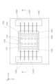
- Fig. 5 is an explanatory diagram showing the top configuration of light source 122a in the second embodiment
- Fig. 6 is an explanatory diagram showing the cross-sectional configuration of light source 122 at the position VI-VI in Fig. 5.
- the description of the same configurations as measuring device 110 of the above-mentioned first embodiment will be omitted as appropriate.
- the light source 122a has a different configuration from the light source 122 in the first embodiment. Specifically, the light source 122a is different in that the light source 122 does not include a protective portion 1310. However, in the second embodiment, the light source 122a also has a configuration for suppressing the cathode of the surface light emitting element 1110 from being short-circuited to the conductive member via the joint portion 1300.
- the light source 122a further satisfies the following first condition.
- First condition> When viewed from the top to bottom, the outer surface S1 of the joint 1300 is located inside the outer edge of the light-emitting chip 1100 (see Figure 5), and the connection portion 1252 between the wire 1250 and the upper surface 1101 (connection area 1105) of the light-emitting chip 1100 is located inside the outer surface S1 of the joint 1300. 6, a first distance D1 from the central axis C of the light-emitting chip 1100 to the outer peripheral surface S1 of the joint portion 1300 is shorter than a second distance D2 from the central axis C to the outer peripheral surface of the light-emitting chip 1100. In addition, a third distance D3 from the central axis C to the connection portion 1252 is shorter than the first distance D1.
- the light source 22a further satisfies the following second condition.
- ⁇ Second condition> When viewed from the vertical direction, the periphery of the light-emitting region 1103 of the light-emitting chip 1100 is located inside the outer peripheral surface S1 of the joint 1300, and the inclination angle ⁇ that a virtual plane L passing through the ridge line of the light-emitting region 1103 and the ridge line of the outer peripheral surface S1 of the joint 1300 makes with respect to the vertical direction is 45 degrees or more. 6, a fourth distance D4 from the central axis C to the periphery of the light emitting region 1103 is shorter than the first distance D1.
- the inclination angle ⁇ of the imaginary plane L with respect to the central axis C is 45 degrees or more.
- the outer peripheral surface S1 of the joint 1300 is located inside the outer edge of the light emitting chip 1100 when viewed in the vertical direction (see FIG. 5, first condition). Therefore, compared to a configuration in which the joint 1300 protrudes outside the light emitting chip 1100, for example, it is possible to suppress the cathode of the surface light emitting element 1110 from being short-circuited to the conductive member via the joint 1300.
- the outer edge of the first conductive pattern 1210 is also located inside the outer edge of the light emitting chip 1100 when viewed in the vertical direction (see FIG. 6).
- connection portion 1252 between the wire 1250 and the upper surface 1101 of the light-emitting chip 1100 is located inside the outer peripheral surface S1 of the joint portion 1300 (first condition). According to this embodiment, for example, compared to a configuration in which the connection portion 1252 is located outside the outer peripheral surface S1 of the joint portion 1300, it is possible to suppress damage to the light-emitting chip 1100 caused by application of a load to the connection portion 1252 of the light-emitting chip 1100.
- the periphery of the light-emitting region 1103 of the light-emitting chip 1100 is located inside the outer peripheral surface S1 of the joint 1300, and the inclination angle ⁇ of the imaginary plane L passing through the ridge of the light-emitting region 1103 and the ridge of the outer peripheral surface S1 of the joint 1300 with respect to the vertical direction is 45 degrees or more (second condition).
- the radiation angle at which the heat generated in the light-emitting region 1103 diffuses toward the lower surface 1102 of the light-emitting chip 1100 is 45 degrees or less with respect to the central axis C. Therefore, according to this embodiment, the heat generated in the light-emitting region 1103 can be effectively released to the outside by the joint 1300, compared to a configuration in which the inclination angle ⁇ is less than 45 degrees, for example.
- the configurations of the measuring device 110 and the light sources 122, 122a in the above embodiment are merely examples and can be modified in various ways.
- the light sources 122, 122a are illustrated as having a plurality of surface light emitting elements 1110 arranged thereon, but the light source may be configured to have a single surface light emitting element arranged thereon.
- the protective section 1310 has a joining function for joining the light emitting chip 1100 and the substrate 1200 (first conductive pattern 1210), but it may not have this joining function.
- the protective section 1310 may be fixedly disposed on the substrate 1200 and not joined to the light emitting chip 1100.
- the protective section 1310 is preferably in contact with the light emitting chip 1100, but may not be in contact with the light emitting chip 1100 and may cover only the lower part of the outer circumferential surface S1 of the joint section 1300.
- the protective part 1310 covers the entire outer surface S1 of the joint 1300, but the protective part 1310 only needs to cover at least a part of the outer surface S1 of the joint 1300.
- the protective part 1310 may be configured to cover only the connection area 1105 side of the outer surface S1 of the joint 1300. This effectively prevents the cathode of the surface-emitting element 1110 from shorting out to the wire 1250 via the joint 1300.
- the protective portion 1310 may not be in contact with the joint 1300. However, if the protective portion 1310 is in contact with the joint 1300, the heat dissipation property of dissipating heat generated at the joint 1300 by energization to the outside via the protective portion 1310 can be improved.
- the area of the exposed surface S2 of the protruding portion 1314 may be equal to or smaller than the contact area between the joint 1300 and the protective portion 1310.
- the exposed surface S2 of the protruding portion 1314 is not limited to a tapered surface, and may be a flat surface along the vertical direction or a curved surface.
- the configuration may not satisfy either the first condition or the second condition.
- the outer edge of the first conductive pattern 1210 may be located outside the outer edge of the light-emitting chip 1100 when viewed from the top to bottom.
- each component is merely examples, and the components may be formed from other materials.
- D-1. Configuration of the measuring device 210 7 is a block diagram showing a schematic configuration of the measuring device 210 in this embodiment. As shown in FIG. 7, the measuring device 210 includes a projector 220 that irradiates the measurement object W with emitted light L1 (e.g., a light beam (laser light)) and a receiver 230 that receives reflected light L2 (return light) that is reflected by the measurement object W and returns from the emitted light L1, and functions as a flash LiDAR.
- L1 e.g., a light beam (laser light)
- L2 return light
- the measuring device 210 is mounted, for example, on a vehicle (not shown) equipped with AD or ADAS.
- the measuring device 210 assists in the detection of objects such as people and other vehicles while the vehicle is traveling, and provides various information to other devices and users that is useful for ensuring the safety of the driver of the vehicle and those around the vehicle, and for reducing damage to surrounding objects while the vehicle is being driven.
- the floodlight 220 has a light source 222, a floodlight optical system 224, a floodlight control device 226, and a current source 228.
- the current source 228 supplies a current corresponding to a control signal input from the light projection control device 226 to the semiconductor laser 223 that constitutes the light source 222.
- the current source 228 supplies, for example, a periodic square wave current to the semiconductor laser 223 for turning on and off the current flowing through the semiconductor laser 223.
- the light-projection control device 226 generates a control signal for controlling the current source 228 and inputs the control signal to the current source 228, thereby controlling the current (drive current) supplied from the current source 228 to the semiconductor laser 223.
- the light-projection control device 226 inputs a signal indicating the timing of light projection at which the semiconductor laser 223 emits light to the TOF measurement device 40.
- the light-projection control device 226 periodically and repeatedly controls the on-off of the current flowing through the semiconductor laser 223, for example, thereby causing the semiconductor laser 223 to emit light periodically and repeatedly.
- the projection optical system 224 adjusts the light distribution of the emitted light L1, for example, by applying optical effects (such as refraction, scattering, and diffraction) to the light emitted by the light source 222.
- the projection optical system 224 is configured using optical components, such as various lenses, such as collimating lenses, and reflectors (mirrors).
- the receiver 230 has a light receiving section 232, a filter 233, and a light receiving optical system 234.
- the light receiving unit 232 is a receiving light source having one or more light receiving elements (not shown), or one or more light receiving element arrays (e.g., light receiving elements arranged linearly (one-dimensionally) or planarly (two-dimensionally)).
- the light receiving elements are, for example, photodiodes, SPADs (Single Photon Avalanche Diodes), balanced photodetectors, etc.
- the light receiving unit 232 photoelectrically converts the reflected light L2 incident from the light receiving optical system 234 to generate a current (hereinafter referred to as the "receiving current") according to the intensity of the reflected light L2.
- the light receiving unit 232 inputs a signal indicating the timing (hereinafter referred to as the "receiving timing") at which the light receiving elements constituting the light receiving unit 232 receive the reflected light L2, and the receiving current generated by the light receiving elements, to the TOF measurement device 40.
- the filter 233 is a wavelength filter that passes laser light of a specific pass band, for example a bandpass filter.
- the specific pass band of the filter 233 will be explained later.
- the filter 233 is disposed between the light receiving optical system 234 and the light receiving unit 232.
- the measurement device 210 further includes a TOF measurement device 40, a controller 42, and a communication I/F (Inter face) 50. Information generated by the controller 42 is provided (transmitted) to various utilization devices 60 via the communication I/F 50.
- Specific passband of filter 233 A specified wavelength band B is indicated on the specification sheet of the semiconductor laser 223.
- the specified wavelength band B is a variation range (bandwidth) that is assumed in advance for the wavelength of the laser light (emitted light L1) emitted by the semiconductor laser 223.
- the specified wavelength band B is specified based on, for example, manufacturing variations of the semiconductor laser 223.
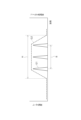
- FIG. 8 is an explanatory diagram showing the prescribed wavelength band B of the semiconductor laser 223.
- the horizontal axis of FIG. 8 shows the wavelength band of light
- the left vertical axis shows the laser intensity of the laser light (emitted light L1) emitted by the semiconductor laser 223, and the right vertical axis shows the filter transmittance of the filter 233 (the same applies to FIGS. 10 to 12 described below).
- Graph G1 in FIG. 8 shows the results of measuring the laser intensity of the laser light for multiple semiconductor lasers 223 (the same applies to FIGS. 10 to 12 described below).
- the peak wavelengths at which the laser intensity peaks are different for the multiple semiconductor lasers 223.
- the wavelengths (peak wavelengths) of the laser light vary for the multiple semiconductor lasers 223.
- the prescribed wavelength band B is a band that includes the range of variation in the peak wavelength that is assumed in advance for the semiconductor laser 223.
- Graph G2 in FIG. 8 shows the filter transmittance (the same applies to FIGS. 11 and 12 described below).
- Symbol H in FIG. 8 is the passband H of the filter of the comparative example.
- the passband H of the filter of the comparative example is set to a bandwidth that includes the specified wavelength band B. Therefore, the laser light emitted by all semiconductor lasers 223 whose peak wavelengths belong to the specified wavelength band B passes through the filter of the comparative example and is received by the light receiving unit 232.
- the passband H of the filter of the comparative example is set to a wide bandwidth that includes the specified wavelength band B.
- the specific passband of the filter 233 is a part of the specified wavelength band B.
- the specific passband of the filter 233 includes the peak wavelength of the laser light emitted by the semiconductor laser 223 implemented in the measurement device 210.
- the bandwidth of the specific passband of the filter 233 is 1/2 or less of the bandwidth of the specified wavelength band B.
- Fig. 9 is a flow chart showing a part of the manufacturing process of the measurement device 210
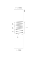
- Fig. 10 is an explanatory diagram showing the classification of the prescribed wavelength band B.
- the prescribed wavelength band B is divided into three wavelength classes f1 to f3.
- the three wavelength classes f1 to f3 are wavelength bands obtained, for example, by equally dividing the prescribed wavelength band B into three.
- the peak wavelength of a semiconductor laser 223 selected from the plurality of semiconductor lasers 223 (hereinafter, sometimes referred to as the "selected semiconductor laser 223") is measured (S2110).
- the selected semiconductor laser 223 is caused to emit light, and the peak wavelength of the laser light emitted by the selected semiconductor laser 223 is measured by a known wavelength measuring device (such as an optical wavelength meter).
- S2120 it is determined which wavelength class the peak wavelength of the selected semiconductor laser 223 belongs to. From the measurement results in S2110, it is determined which of the three wavelength classes f1 to f3 the selected semiconductor laser 223 belongs to. Note that at least a portion of the steps S2110 and S2120 may be performed manually by a person, or may be performed automatically by a machine such as a robot.
- FIG. 11 is an explanatory diagram showing a specific pass band H1 for the first wavelength class f1
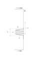
- FIG. 12 is an explanatory diagram showing a specific pass band H2 for the second wavelength class f2.
- the specific pass band H1 of the filter 233 when the peak wavelength of the selected semiconductor laser 223 belongs to the first wavelength class f1, the specific pass band H1 of the filter 233 is a band whose bandwidth is narrower than the specified wavelength band B and includes the first wavelength class f1.
- the specific pass band H2 of the filter 233 is a band whose bandwidth is narrower than the specified wavelength band B and includes the second wavelength class f2.
- the selected semiconductor laser 223 is placed in the light projector 220, and the corresponding filter 233 is placed in the light receiver 230 (S2140). After that, the remaining assembly steps are performed, and the manufacture of the measuring device 210 is completed. With this manufacturing method, it is possible to efficiently manufacture the measuring device 210 in which the effects of noise are more effectively suppressed.
- the specific pass band of the filter 233 is a part of the prescribed wavelength band B.
- the specific pass band of the filter 233 includes the peak wavelength of the laser light emitted by the semiconductor laser 223 mounted on the measuring device 210. Therefore, according to this embodiment, compared to a configuration in which the specific pass band of the filter 233 is the same as the prescribed wavelength band B, the influence of noise such as sunlight is suppressed, and the measurable distance can be improved.
- the bandwidth of the specific passband of the filter 233 is equal to or less than half the bandwidth of the specified wavelength band B. This makes it possible to more effectively suppress the effects of noise.
- the configurations of the measuring device 210, the light projector 220, and the light receiver 230 in the above embodiment are merely examples, and various modifications are possible.
- the filter 233 was placed between the light receiving optical system 234 and the light receiving section 232, but it may be placed in front of the light receiving optical system 234, or may be incorporated as a part of the light receiving optical system 234.
- the measuring device 210 is configured to include one semiconductor laser 223 and one filter 233, but this is not limited thereto, and may be configured to include multiple semiconductor lasers and multiple filters corresponding to each of the multiple semiconductor lasers.
- the projector 220 may have a first semiconductor laser and a second semiconductor laser, and the projector 220 may have a first filter that passes the laser light emitted by the first semiconductor laser and a second filter that passes the laser light emitted by the second semiconductor laser.
- it is preferable that the first semiconductor laser and the second semiconductor laser have the same specified wavelength band, and the first filter and the second filter have different specific pass bands.
- the specific pass band of the first filter is the specific pass band H1 corresponding to the first wavelength class f1.
- the specific passband of the first filter is the specific passband H2 corresponding to the first wavelength class f2.
- the bandwidth of the specific passband of filter 233 is 1/2 or less of the bandwidth of specified wavelength band B, but this is not limited thereto, and may be, for example, 1/3 or less of the bandwidth of specified wavelength band B, or 1/5 or less of the bandwidth of specified wavelength band B.
- the lower limit of the bandwidth of the specific passband of filter 233 is not particularly limited, and may be, for example, 1/100 or more, or 1/20 or more of the bandwidth of specified wavelength band B.
- the specified wavelength band B is divided equally into three and separated into three wavelength classes f1 to f3, but this is not limited thereto, and the specified wavelength band B may be separated into two wavelength classes, or into four or more wavelength classes. Furthermore, the bandwidths of at least two of the multiple wavelength classes may differ from each other.
- each component is merely examples, and the components may be formed from other materials.
- the multiple embodiments disclosed in this specification can be combined as appropriate, and configurations obtained by combining them are also included in this disclosure.
- the light source 122 in the first embodiment or the light source 122a in the second embodiment may be used as the light source 222 in the measurement device 210 in the third embodiment.
Landscapes
- Physics & Mathematics (AREA)
- General Physics & Mathematics (AREA)
- Engineering & Computer Science (AREA)
- Electromagnetism (AREA)
- Condensed Matter Physics & Semiconductors (AREA)
- Optics & Photonics (AREA)
- Computer Networks & Wireless Communication (AREA)
- Radar, Positioning & Navigation (AREA)
- Remote Sensing (AREA)
- Led Device Packages (AREA)
Abstract
Une source de lumière (122) comprend : une puce électroluminescente (1100) dans laquelle un élément électroluminescent de surface (1110) est disposé, la puce électroluminescente (1100) comportant une première surface (1102) qui est électriquement connectée à la cathode de l'élément électroluminescent de surface (1110), et une seconde surface (1101) qui est électriquement connectée à l'anode de l'élément électroluminescent de surface (1110) ; un substrat (1200) dans lequel un premier motif conducteur (1210) et un second motif conducteur (1220) sont formés ; une partie de jonction conductrice (1300) qui relie la première surface (1102) de la puce électroluminescente (1100) et le premier motif conducteur (1210) ; et un fil (1250) qui connecte électriquement la seconde surface (1101) de la puce électroluminescente (1100) et le second motif conducteur (1220). La source de lumière (122) comprend en outre une partie de protection non conductrice (1310) qui est disposée sur le côté périphérique externe de la partie de jonction (1300) et qui recouvre au moins une partie de la surface périphérique externe de la partie de jonction (1300).
Priority Applications (1)
| Application Number | Priority Date | Filing Date | Title |
|---|---|---|---|
| CN202480047306.4A CN121532915A (zh) | 2023-07-18 | 2024-07-16 | 光源、测定装置、光源的制造方法以及测定装置的制造方法 |
Applications Claiming Priority (4)
| Application Number | Priority Date | Filing Date | Title |
|---|---|---|---|
| JP2023-116441 | 2023-07-18 | ||
| JP2023116439A JP2025014157A (ja) | 2023-07-18 | 2023-07-18 | 光源、測定装置、および、光源の製造方法 |
| JP2023116441A JP2025014158A (ja) | 2023-07-18 | 2023-07-18 | 測定装置、および、測定装置の製造方法 |
| JP2023-116439 | 2023-07-18 |
Publications (1)
| Publication Number | Publication Date |
|---|---|
| WO2025018351A1 true WO2025018351A1 (fr) | 2025-01-23 |
Family
ID=94282168
Family Applications (1)
| Application Number | Title | Priority Date | Filing Date |
|---|---|---|---|
| PCT/JP2024/025538 Ceased WO2025018351A1 (fr) | 2023-07-18 | 2024-07-16 | Source de lumière, dispositif de mesure, procédé de fabrication de source de lumière et procédé de fabrication de dispositif de mesure |
Country Status (2)
| Country | Link |
|---|---|
| CN (1) | CN121532915A (fr) |
| WO (1) | WO2025018351A1 (fr) |
Citations (11)
| Publication number | Priority date | Publication date | Assignee | Title |
|---|---|---|---|---|
| JP2015153862A (ja) * | 2014-02-13 | 2015-08-24 | 株式会社リコー | 面発光レーザアレイ及びレーザ装置 |
| JP2020174097A (ja) * | 2019-04-10 | 2020-10-22 | 富士ゼロックス株式会社 | 発光装置、光学装置及び情報処理装置 |
| US20210116567A1 (en) * | 2019-10-18 | 2021-04-22 | Ai4 International Oy | Measurement device and method of operating therefor |
| JP2021105613A (ja) | 2017-07-28 | 2021-07-26 | オプシス テック リミテッド | 小角度発散を伴うvcselアレイlidar送信機 |
| JP2021136306A (ja) * | 2020-02-26 | 2021-09-13 | 富士フイルムビジネスイノベーション株式会社 | 発光装置、光学装置及び情報処理装置 |
| JP2021150628A (ja) * | 2020-03-24 | 2021-09-27 | 富士フイルムビジネスイノベーション株式会社 | 発光装置、光学装置、計測装置及び情報処理装置 |
| JP2021153135A (ja) * | 2020-03-24 | 2021-09-30 | 富士フイルムビジネスイノベーション株式会社 | 発光装置、光学装置、計測装置及び情報処理装置 |
| JP2021197404A (ja) * | 2020-06-10 | 2021-12-27 | スタンレー電気株式会社 | 発光装置 |
| JP2023067922A (ja) * | 2016-06-06 | 2023-05-16 | パイオニア株式会社 | 装置および方法 |
| JP2023116441A (ja) | 2008-10-24 | 2023-08-22 | 株式会社半導体エネルギー研究所 | 半導体装置 |
| JP2023116439A (ja) | 2023-04-25 | 2023-08-22 | 株式会社ニューギン | 遊技機 |
-
2024
- 2024-07-16 WO PCT/JP2024/025538 patent/WO2025018351A1/fr not_active Ceased
- 2024-07-16 CN CN202480047306.4A patent/CN121532915A/zh active Pending
Patent Citations (11)
| Publication number | Priority date | Publication date | Assignee | Title |
|---|---|---|---|---|
| JP2023116441A (ja) | 2008-10-24 | 2023-08-22 | 株式会社半導体エネルギー研究所 | 半導体装置 |
| JP2015153862A (ja) * | 2014-02-13 | 2015-08-24 | 株式会社リコー | 面発光レーザアレイ及びレーザ装置 |
| JP2023067922A (ja) * | 2016-06-06 | 2023-05-16 | パイオニア株式会社 | 装置および方法 |
| JP2021105613A (ja) | 2017-07-28 | 2021-07-26 | オプシス テック リミテッド | 小角度発散を伴うvcselアレイlidar送信機 |
| JP2020174097A (ja) * | 2019-04-10 | 2020-10-22 | 富士ゼロックス株式会社 | 発光装置、光学装置及び情報処理装置 |
| US20210116567A1 (en) * | 2019-10-18 | 2021-04-22 | Ai4 International Oy | Measurement device and method of operating therefor |
| JP2021136306A (ja) * | 2020-02-26 | 2021-09-13 | 富士フイルムビジネスイノベーション株式会社 | 発光装置、光学装置及び情報処理装置 |
| JP2021150628A (ja) * | 2020-03-24 | 2021-09-27 | 富士フイルムビジネスイノベーション株式会社 | 発光装置、光学装置、計測装置及び情報処理装置 |
| JP2021153135A (ja) * | 2020-03-24 | 2021-09-30 | 富士フイルムビジネスイノベーション株式会社 | 発光装置、光学装置、計測装置及び情報処理装置 |
| JP2021197404A (ja) * | 2020-06-10 | 2021-12-27 | スタンレー電気株式会社 | 発光装置 |
| JP2023116439A (ja) | 2023-04-25 | 2023-08-22 | 株式会社ニューギン | 遊技機 |
Also Published As
| Publication number | Publication date |
|---|---|
| CN121532915A (zh) | 2026-02-13 |
Similar Documents
| Publication | Publication Date | Title |
|---|---|---|
| US11862929B2 (en) | Laser diode packaging module, distance detection device, and electronic device | |
| JP7082043B2 (ja) | レーザダイオードを用いた特殊一体型光源 | |
| US11609311B2 (en) | Pulsed light irradiation/detection device, and optical radar device | |
| US11710945B2 (en) | Projection of patterned and flood illumination | |
| US20220114835A1 (en) | Light-emitting device, optical device, and information processing device | |
| JPH09222540A (ja) | 高さの低い光学的サブアセンブリ | |
| KR102523975B1 (ko) | 광원 일체형 광 센싱 시스템 및 이를 포함하는 전자 기기 | |
| US12483002B2 (en) | Semiconductor laser device | |
| JP2016092364A (ja) | 発光装置及び灯具 | |
| CN112993744B (zh) | 光源装置 | |
| US12149050B2 (en) | Low divergence vertical cavity surface emitting lasers, and modules and host devices incorporating the same | |
| CN113079708A (zh) | 激光二极管封装模块及距离探测装置、电子设备 | |
| CN109655806A (zh) | 传感器设备 | |
| JP2004152875A (ja) | 半導体レーザモジュール | |
| US11502479B2 (en) | Optical device, light-source device, detector, and electronic device | |
| JP2025014157A (ja) | 光源、測定装置、および、光源の製造方法 | |
| CN121532915A (zh) | 光源、测定装置、光源的制造方法以及测定装置的制造方法 | |
| US12548972B2 (en) | Light source module, distance-measuring apparatus, and mobile object | |
| KR20190142576A (ko) | 표면발광 레이저패키지 및 이를 포함하는 광 모듈 | |
| JP6734654B2 (ja) | 受光モジュール及び受光モジュールの製造方法 | |
| WO2024094469A1 (fr) | Système de capteur optique actif à dissipation de chaleur | |
| WO2022255146A1 (fr) | Dispositif émetteur de lumière et dispositif de mesure de distance | |
| US11867375B2 (en) | Radiation-emitting semiconductor chip, rear light for a motor vehicle, motor vehicle, and optical distance measurement device | |
| JPWO2018180658A1 (ja) | 波長変換素子及び発光装置 | |
| JP2023116281A (ja) | 投光器、及び測定装置 |
Legal Events
| Date | Code | Title | Description |
|---|---|---|---|
| 121 | Ep: the epo has been informed by wipo that ep was designated in this application |
Ref document number: 24843141 Country of ref document: EP Kind code of ref document: A1 |
|
| WWE | Wipo information: entry into national phase |
Ref document number: 2024843141 Country of ref document: EP |
|
| NENP | Non-entry into the national phase |
Ref country code: DE |