WO2025028131A1 - 積層セラミックコンデンサ - Google Patents
積層セラミックコンデンサ Download PDFInfo
- Publication number
- WO2025028131A1 WO2025028131A1 PCT/JP2024/023950 JP2024023950W WO2025028131A1 WO 2025028131 A1 WO2025028131 A1 WO 2025028131A1 JP 2024023950 W JP2024023950 W JP 2024023950W WO 2025028131 A1 WO2025028131 A1 WO 2025028131A1
- Authority
- WO
- WIPO (PCT)
- Prior art keywords
- multilayer ceramic
- ceramic capacitor
- laminate
- end surface
- electrode
- Prior art date
- Legal status (The legal status is an assumption and is not a legal conclusion. Google has not performed a legal analysis and makes no representation as to the accuracy of the status listed.)
- Pending
Links
Images


Classifications
-
- H—ELECTRICITY
- H01—ELECTRIC ELEMENTS
- H01G—CAPACITORS; CAPACITORS, RECTIFIERS, DETECTORS, SWITCHING DEVICES, LIGHT-SENSITIVE OR TEMPERATURE-SENSITIVE DEVICES OF THE ELECTROLYTIC TYPE
- H01G4/00—Fixed capacitors; Processes of their manufacture
- H01G4/30—Stacked capacitors
-
- H—ELECTRICITY
- H01—ELECTRIC ELEMENTS
- H01G—CAPACITORS; CAPACITORS, RECTIFIERS, DETECTORS, SWITCHING DEVICES, LIGHT-SENSITIVE OR TEMPERATURE-SENSITIVE DEVICES OF THE ELECTROLYTIC TYPE
- H01G4/00—Fixed capacitors; Processes of their manufacture
- H01G4/35—Feed-through capacitors or anti-noise capacitors
Definitions
- the present invention relates to a multilayer ceramic capacitor.
- a three-terminal multilayer ceramic capacitor comprises an inner layer portion in which dielectric layers having end surface exposed internal electrodes arranged on end surfaces and dielectric layers having side surface internal electrodes arranged on side surfaces are alternately stacked, and outer layer portions arranged on one side and the other side in a stacking direction of the inner layer portion; and external electrodes including end surface external electrodes arranged on the end surfaces and connected to the end surface exposed internal electrodes, and side surface external electrodes arranged on the side surfaces and connected to the side surface internal electrodes (see Patent Document 1).
- a three-terminal multilayer ceramic capacitor can have lower impedance at high frequencies by being made smaller.
- the lower impedance achieved by making the capacitor smaller is due to a decrease in the equivalent series inductance (hereinafter referred to as "ESL") of the multilayer ceramic capacitor.
- ESL equivalent series inductance
- An object of the present invention is to provide a multilayer ceramic capacitor in which external electrodes are not easily peeled off from the laminate.
- the present invention provides a multilayer ceramic capacitor that includes a laminate having an inner layer portion in which dielectric layers and internal electrodes are alternately laminated in a plurality of layers, and outer layer portions arranged on one side and the other side of the lamination direction of the inner layer portion, and an external electrode that is provided on at least one surface of the laminate in a direction intersecting the lamination direction and includes a main surface side folded portion that covers a part of the outer layer portion, and a multilayer ceramic capacitor in which a mixed layer of dielectric and metal is provided in the covering portion of the outer layer portion that is covered by the main surface side folded portion.
- the present invention provides a multilayer ceramic capacitor in which the external electrodes are less likely to peel off from the laminate.
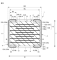
- FIG. 1 is a schematic perspective view of a multilayer ceramic capacitor 1.
- FIG. 2 is a cross-sectional view of the multilayer ceramic capacitor 1 according to the embodiment taken along line II-II in FIG. 3 is a cross-sectional view of the multilayer ceramic capacitor 1 according to the embodiment taken along the line III-III in FIG. 2 is a cross-sectional view taken along an end surface exposed internal electrode 15A of the multilayer ceramic capacitor 1.
- FIG. 2 is a cross-sectional view taken along a side surface exposed internal electrode 15B of the multilayer ceramic capacitor 1.
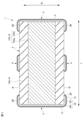
- FIG. 4 is a cross-sectional view of an embodiment of the multilayer ceramic capacitor 1 taken along the IV-IV direction in the portion of the outer layer 12 in FIG. 1.
- 2A to 2C are diagrams illustrating a manufacturing process of a laminate 2 in a manufacturing method of a multilayer ceramic capacitor 1.
- 2 is a flowchart illustrating a method for manufacturing the multilayer ceramic capacitor 1.
- FIG. 1 is a schematic perspective view of the multilayer ceramic capacitor 1.
- FIG. 2 is a cross-sectional view of an embodiment of the multilayer ceramic capacitor 1 cut in the II-II direction in FIG. 1.
- FIG. 3 is a cross-sectional view of an embodiment of the multilayer ceramic capacitor 1 cut in the III-III direction in FIG. 1.
- the multilayer ceramic capacitor 1 is a three-terminal multilayer ceramic capacitor 1 including a laminate 2, end surface external electrodes 3 provided on both end surfaces C in the length direction L of the laminate 2, and side surface external electrodes 4 provided on both side surfaces B in the width direction W of the laminate 2.
- the laminate 2 includes an inner layer portion 11 in which a dielectric layer 14 and an internal electrode 15 are laminated, and an outer layer portion 12.
- the terminology used to indicate the orientation of the multilayer ceramic capacitor 1 refers to the direction in which the dielectric layers 14 and internal electrodes 15 are stacked in the multilayer ceramic capacitor 1 as the stacking direction T.
- the direction that intersects with the stacking direction T and in which the pair of end face external electrodes 3 are provided is referred to as the length direction L.
- the direction that intersects with both the length direction L and the stacking direction T is referred to as the width direction W.
- the stacking direction T, the length direction L, and the width direction W are mutually orthogonal.
- a pair of outer surfaces on both sides of the stacking direction T are referred to as main surfaces A
- a pair of outer surfaces extending in the stacking direction T and on both sides of the width direction W are referred to as side surfaces B
- a pair of outer surfaces extending in the stacking direction T and on both sides of the length direction L are referred to as end surfaces C.
- the multilayer ceramic capacitor 1 is shown in FIG.
- the dimension LC in the length direction L is 0.10 mm or more and 0.70 mm or less
- the dimension WC in the width direction W is 0.05 mm or more and 0.40 mm or less
- the dimension TC in the stacking direction T is 0.10 mm or more and 0.55 mm or less.
- the capacitance of the multilayer ceramic capacitor 1 is 0.022 ⁇ F or more and 10 ⁇ F or less, and preferably 1.0 ⁇ F or more and 2.2 ⁇ F or less.
- the ESL of the multilayer ceramic capacitor 1 is preferably 65 pH or less at 100 MHz, and 50 pH or less at 1 GHz.
- the capacitance of the multilayer ceramic capacitor 1 can be measured using an LCR meter (manufactured by Agilent Technologies, model number: E4980A) under conditions of 1 kHz and 0.5 Vrms.
- the ESL of the multilayer ceramic capacitor 1 can be calculated from the measured impedance value at a specified frequency using a network analyzer (manufactured by Agilent Technologies, model number: E5080A).
- the laminate 2 includes an inner layer portion 11 and outer layer portions 12 disposed on both sides of the inner layer portion 11 in the stacking direction T.
- the corners and ridges of the laminate 2 are preferably rounded. The corners are portions where three faces of the laminate 2 intersect, and the ridges are portions where two faces of the laminate 2 intersect.
- the dimensions of the laminate 2 are as shown in FIG.
- the dimension LL in the length direction L is 0.09 mm or more and 0.69 mm or less
- the dimension WL in the width direction W is 0.04 mm or more and 0.39 mm or less
- the dimension TL in the stacking direction T is 0.09 mm or more and 0.54 mm or less.
- the inner layer portion 11 includes a plurality of dielectric layers 14 and internal electrodes 15 laminated in a lamination direction T.
- the dielectric layer 14 is made of a ceramic material.
- the ceramic material used is one that contains at least one of Ca, Zr, and Ti as its main component.
- the main component is, for example, a ceramic material having a perovskite structure represented by the general formula ABO 3 containing Ca and Zr. Examples of ceramic materials having such a perovskite structure include, but are not limited to, BaTiO 3 (barium titanate) and CaZrO 3 (calcium zirconate).
- the main component of the ceramic material forming the dielectric layer 14 may contain all of Ca, Zr, and Ti.
- the internal electrodes 15 are preferably made of a metal material such as Ni, Cu, Ag, Pd, an Ag-Pd alloy, or Au.
- the internal electrode 15 has a plurality of end-exposed internal electrodes 15A and a plurality of side-exposed internal electrodes 15B arranged alternately. When there is no need to distinguish between the end-exposed internal electrodes 15A and the side-exposed internal electrodes 15B, they will be collectively referred to as the internal electrodes 15.
- FIG. 4 is a cross-sectional view along the end-face exposed internal electrode 15A of the multilayer ceramic capacitor 1.
- FIG. 5 is a cross-sectional view along the side-face exposed internal electrode 15B of the multilayer ceramic capacitor 1.
- End face exposed internal electrode 15A As shown in Fig. 4, the end surface exposed internal electrode 15A extends between both end faces C in the length direction L of the laminate 2 and is spaced a certain distance from both side faces B in the width direction W.
- the end surface exposed internal electrode 15A has an end surface facing portion 15Aa located in the center between both end faces C and an end surface drawn portion 15Ab extending from the end surface facing portion 15Aa to both end faces C.
- the end surface facing portion 15Aa and the end surface drawn portion 15Ab have the same dimension in the width direction W, and the end surface exposed internal electrode 15A is substantially rectangular as a whole including the end surface facing portion 15Aa and the end surface drawn portion 15Ab.
- the end surface drawn portions 15Ab extending from the end surface facing portion 15Aa to both end faces C extend to both end faces C, respectively, are exposed at the end faces C of the laminate 2, and are connected to the end surface external electrodes 3 provided on both end faces C in the length direction L of the laminate 2.
- the side surface exposed internal electrode 15B has a side surface facing portion 15Ba located in the center between both side surfaces B, and a side surface drawn portion 15Bb extending from the side surface facing portion 15Ba to both side surfaces B.
- the side surface facing portion 15Ba is a substantially rectangular shape slightly smaller than the laminate 2, and is spaced a certain distance from both side surfaces B in the width direction W.
- the dimension of the side extension portion 15Bb in the length direction L is smaller than the dimension of the side facing portion 15Ba in the length direction L.
- the side extension portion 15Bb extends to both side surfaces B, is exposed to the side surface B of the laminate 2, and is connected to the side external electrodes 4 provided on both side surfaces of the laminate 2 in the width direction W.
- the end surface facing portion 15Aa and the side surface facing portion 15Ba face each other and form a capacitor portion.
- the dielectric layer 14 is formed by alternately stacking multiple layers of a first dielectric layer 14A having an end-surface-exposed internal electrode 15A exposed on the end surface C, and a second dielectric layer 14B having a side-surface-exposed internal electrode 15B exposed on a portion of the side surface B.
- the outer layer portion 12 is a dielectric layer disposed on the main surface A side of the inner layer portion 11.
- the outer layer portion 12 is made of the same material as the dielectric layer 14 of the inner layer portion 11.
- End surface external electrode 3 End surface external electrodes 3 are disposed on both end surfaces C of the laminate 2. To the end surface external electrodes 3, end surface drawn portions 15Ab of end surface exposed internal electrodes 15A are connected.
- Side external electrode 4 Side surface external electrodes 4 are disposed on both side surfaces B of the laminate 2. To the side surface external electrodes 4, side surface drawn portions 15Bb of side surface exposed internal electrodes 15B are connected.
- the end face external electrode 3 and the side face external electrode 4 include a base electrode layer 31 and a plating layer 32 arranged on the base electrode layer 31.
- the plating layer 32 includes a Ni (nickel) plating layer 321 arranged on the base electrode layer 31 and a Sn (tin) plating layer 322 arranged on the Ni plating layer 321.
- the end face external electrode 3 and the side face external electrode 4 may have a structure in which, for example, the base electrode layer 31 is made of Ni, and a Cu plating layer, a Ni plating layer, and a Sn plating layer are arranged on top of it in that order.
- the end face external electrode 3 includes an end face electrode main surface side folded portion 3A that covers not only the end face C but also a part of the main surface A, and an end face electrode side surface side folded portion 3B that covers a part of the side surface B.
- the side surface external electrode 4 includes a side surface electrode main surface side folded portion 4A that covers not only the side surface B but also a part of the main surface A.
- (Mixed layer) 6 is a cross-sectional view of an embodiment in which the portion of the outer layer portion 12 in FIG. 1 of the multilayer ceramic capacitor 1 is cut in the IV-IV direction.
- An end surface side mixed layer 12Aa is provided on an end surface side covering portion 16a in the outer layer portion 12 that is covered by an end surface electrode main surface side folded portion 3A of the end surface external electrode 3.
- a side surface side mixed layer 12Ab is provided on a side surface side covering portion 16b in the outer layer portion 12 that is covered by a side surface electrode main surface side folded portion 4A of the side surface external electrode 4.
- covering portion 16a when it is not necessary to distinguish between the end surface side covering portion 16a and the side surface side covering portion 16b, they will be collectively referred to as covering portion 16.
- mixed layer 12A When it is not necessary to distinguish between the end surface side mixed layer 12Aa and the side surface side mixed layer 12Ab, they will be collectively referred to as mixed layer 12A.
- the mixed layer 12A includes a dielectric and a metal.
- the dielectric is the same as the dielectric that constitutes the outer layer 12, and the metal is preferably the same as the metal, such as Cu or Ni, that constitutes the external electrode.
- the ratio of metal to dielectric in mixed layer 12A is 0.001 mol% or more and 50 mol% or less.
- the ratio of metal to dielectric in mixed layer 12A can be measured, for example, by polishing a cross section of mixed layer 12A to expose it, performing a composition analysis using EDX (Energy Dispersive X-ray Spectroscopy), and calculating the ratio from the quantitative calculation values of each composition obtained from the analysis results.
- EDX Electronicgy Dispersive X-ray Spectroscopy
- the area occupied by the mixed layer 12A is 1% to 99% of the total area of the coated portion of the outer layer portion 12. Note that Figures 2 and 3 show a case where the area occupied by the mixed layer 12A is approximately 50% of the total area of the coated portion of the outer layer portion 12.
- the “covered portion of the outer layer portion 12" refers to the end surface side covered portion 16a, which is the area of the outer layer portion 12 covered by the end surface electrode main surface side folded portion 3A of the end surface external electrode 3, and the side surface side covered portion 16b, which is the area covered by the side surface electrode main surface side folded portion 4A of the side surface external electrode 4, as shown in Figures 2 and 3.
- a dimension L1 in the length direction L perpendicular to the end surface C where the end surface external electrode 3 is connected to the end surface exposed internal electrode 15A is 0.05 mm or more and 0.20 mm or less.
- the dimension W1 in the width direction W perpendicular to the side B where the side external electrode 4 is connected to the side exposed internal electrode 15B on the main surface A of the side electrode main surface side folded portion 4A of the side external electrode 4 is 0.05 mm or more and 0.20 mm or less.
- Fig. 7 is a diagram for explaining the steps for manufacturing the laminate 2 in the method for manufacturing the multilayer ceramic capacitor 1.
- Fig. 8 is a flow chart for explaining the method for manufacturing the multilayer ceramic capacitor 1.
- An end surface exposed internal electrode 15A is formed from a conductive paste on a ceramic green sheet 14A' that will become the first dielectric layer 14A.
- a side surface exposed internal electrode 15B is formed from a conductive paste on a ceramic green sheet 14B' that will become the second dielectric layer 14B.
- Ceramic green sheet 14A' and ceramic green sheet 14B' are strip-shaped sheets formed by forming a ceramic slurry containing ceramic powder, binder and solvent onto a carrier film using a die coater, gravure coater, microgravure coater, etc.
- the end-exposed internal electrodes 15A and side-exposed internal electrodes 15B are formed by printing, such as screen printing, gravure printing, letterpress printing, etc.
- Outer layer sheet forming step S2 A small amount of metal powder is printed, for example by inkjet printing, on a portion 16a' that will become the end face side covering portion 16a and a portion 16b' that will become the side face side covering portion 16b of the ceramic green sheet that will become the outer layer portion 12, to prepare a ceramic green sheet 12' for the outer layer portion before lamination.
- Ceramic green sheets 14A' to become the first dielectric layer 14A having end surface exposed internal electrodes 15A arranged thereon and ceramic green sheets 14B' to become the second dielectric layer 14B having side surface exposed internal electrodes 15B arranged thereon are laminated alternately.
- the ceramic green sheets 12' for the outer layers are placed one above the other with the metal powder printed on the outside, and then thermocompression bonded to form a mother block.
- Example electrode formation step S5 Next, side surface external electrodes 4 are formed on both side surfaces B of the laminate 2. Side surface drawn portions 15Bb of side surface exposed internal electrodes 15B are connected to the side surface external electrodes 4. The side surface external electrodes 4 are formed so as to cover not only the side surface B but also a portion of the side surface B side of the main surface A. At this time, the portion 16b' on the laminate 2 where the metal powder is printed is covered by the side surface electrode main surface side folded portion 4A of the side surface external electrodes 4 to become the side surface side covering portion 16b.
- end surface external electrodes 3 are formed on both end surfaces C of the laminate 2. End surface drawn-out portions 15Ab of the end surface exposed internal electrodes 15A are connected to the end surface external electrodes 3.
- the end surface external electrodes 3 are formed so as to cover not only the end surface C, but also a portion of the end surface C side of the main surface A and side surface B. At this time, the portion 16a' on the laminate 2 where the metal powder is printed is covered by the end surface electrode main surface side folded portion 3A of the end surface external electrode 3 to become the end surface side covering portion 16a.
- the laminate is heated in a nitrogen atmosphere for a predetermined time at the set firing temperature.
- the metal powder printed on the end surface side covering portions 16a and the side surface side covering portions 16b in the outer layer ceramic green sheets 12' diffuses into the outer layer portions 12.
- the end surface side mixed layer 12Aa is formed in the end surface side covering portion 16a
- the side surface side mixed layer 12Ab is formed in the side surface side covering portion 16b, thereby producing the multilayer ceramic capacitor 1 of the embodiment.
- an end surface side mixed layer 12Aa is formed in the end surface side covering portion of the outer layer portion 12 that is covered by the end surface electrode main surface side folded portion 3A of the end surface external electrode 3.
- a side surface side mixed layer 12Ab is formed in the side surface side covering portion of the outer layer portion 12 that is covered by the side surface electrode main surface side folded portion 4A of the side surface external electrode 4.
- the end face mixed layer 12Aa which is a mixture of dielectric and metal, is formed in this way, the metal contained in the end face mixed layer 12Aa bonds with the metal contained in the end face external electrode 3, improving the adhesion strength between the end face electrode main surface side folded portion 3A of the end face external electrode 3 and the outer layer portion 12, thereby improving the strength resistance of the multilayer ceramic capacitor 1 against external stress.
- the metal contained in the side mixed layer 12Ab bonds with the metal contained in the side external electrode 4, improving the adhesion strength between the side electrode main surface side folded portion 4A of the side external electrode 4 and the outer layer portion 12, thereby improving the strength resistance of the multilayer ceramic capacitor 1 against external stress.
- a three-terminal multilayer ceramic capacitor 1 has mixed layers 12A provided in four locations on each of the two main surfaces A, namely, on the two end surface external electrodes 3 sides and the two side surface external electrodes 4 sides, for a total of eight locations.
- the mixed layer 12A may be provided on only one of the two main surfaces A sides.
- the mixed layer 12A may be provided in some, but not all, of the four locations on the two end surface external electrodes 3 sides and the two side surface external electrodes 4 sides.
- the multilayer ceramic capacitor may be a two-terminal one.
- the multilayer ceramic capacitor may include the end surface external electrode 3, the end surface electrode main surface side folded portion 3A, and the end surface side mixed layer 12Aa, but not the side surface external electrode 4, the side surface electrode main surface side folded portion 4A, or the side surface side mixed layer 12Ab.
- the mixed layer 12A is provided in the outer layer portion 12, but the mixed layer may be formed in the portion of the inner layer portion 11 that is covered by the folded portion of the dielectric layer 14.
- the present invention also includes the following.
- a laminate having an inner layer portion in which a plurality of dielectric layers and internal electrodes are alternately laminated, and outer layer portions arranged on one side and the other side of the lamination direction of the inner layer portion; an external electrode provided on at least one surface of the laminate in a direction intersecting the lamination direction and including a main surface side folded portion covering a part of the outer layer portion;
- a multilayer ceramic capacitor comprising: a mixed layer of a dielectric and a metal is provided on a covering portion of the outer layer portion that is covered by the main surface side folded portion; Multilayer ceramic capacitor.
- the internal electrodes are an end surface exposed internal electrode exposed at one and the other end surfaces in the longitudinal direction of the laminate; a side surface exposed internal electrode exposed on one and the other side surfaces in the width direction of the laminate,
- the external electrode is an end surface external electrode provided on the end surface of the laminate and connected to the end surface exposed internal electrode; a side surface external electrode provided on the side surface of the laminate and connected to the side surface exposed internal electrode;
- the multilayer ceramic capacitor according to ⁇ 1> which is a three-terminal type having
- the ratio of the metal to the dielectric in the mixed layer is 0.001 mol % or more and 50 mol % or less.
- ⁇ 4> In the laminate, when a direction intersecting the stacking direction is a length direction, and a direction intersecting the stacking direction and the length direction is a width direction, In each of a cross section passing through the stacking direction and the length direction, a cross section passing through the stacking direction and the width direction, and a cross section passing through the length direction and the width direction, an area occupied by the mixed layer is 1% or more and 99% or less of a total area of the covering portion.
- ⁇ 4> The multilayer ceramic capacitor according to any one of ⁇ 1> to ⁇ 3>.
- the internal electrodes are an end surface exposed internal electrode exposed at one and the other end surfaces in the longitudinal direction of the laminate; a side surface exposed internal electrode exposed on one and the other side surfaces in the width direction of the laminate,
- the external electrode is an end surface external electrode provided on the end surface of the laminate and connected to the end surface exposed internal electrode; a side surface external electrode provided on the side surface of the laminate and connected to the side surface exposed internal electrode; It is a three-terminal type having
- the main surface side folded portion is an end surface electrode main surface side folded portion included in the end surface external electrode; a side electrode main surface side folded portion included in the side electrode external electrode,
- the covering portion is an end surface side covering portion covered by the end surface electrode main surface side folded portion; a side surface covering portion covered by the side surface electrode main surface folded portion, the mixed layer is provided on both the end surface side covering portion and the side surface side covering portion
- the main surface side folded portion of the external electrode has a dimension of 0.05 to 0.20 mm in a direction perpendicular to a surface on the main surface where the external electrode is connected to the internal electrode.
- ⁇ 7> The dimension in the stacking direction is 0.55 mm or less
- ⁇ 6> The multilayer ceramic capacitor according to any one of ⁇ 1> to ⁇ 6>.
- the dimension in the length direction intersecting with the stacking direction is 0.10 mm or more and 0.70 mm or less, The dimension in the width direction intersecting the stacking direction and the length direction is 0.05 mm or more and 0.40 mm or less; ⁇ 8> The multilayer ceramic capacitor according to any one of ⁇ 1> to ⁇ 7>.
- the external electrodes contain Ni, ⁇ 9>
- the capacitance is 0.022 ⁇ F or more and 10 ⁇ F or less.
- the equivalent series inductance is 65 pH or less at 100 MHz and 50 pH or less at 1 GHz.
Landscapes
- Engineering & Computer Science (AREA)
- Power Engineering (AREA)
- Manufacturing & Machinery (AREA)
- Microelectronics & Electronic Packaging (AREA)
- Fixed Capacitors And Capacitor Manufacturing Machines (AREA)
- Ceramic Capacitors (AREA)
Abstract
外部電極が積層体から剥がれにくい積層セラミックコンデンサを提供する。誘電体層14と内部電極15とが交互に複数積層された内層部11、及び、前記内層部11の積層方向の一方と他方とに配置された外層部12を有する積層体2と、前記積層体2における、前記積層方向と交差する方向の少なくとも一方の面に設けられるとともに、前記外層部12の一部を覆う主面側折返部3A,4Aを含む外部電極3,4と、を備える積層セラミックコンデンサ1であって、前記外層部12における、前記主面側折返部3A,4Aによって覆われている被覆部16に、誘電体と金属との混合層12Aが設けられている。
Description
本発明は、積層セラミックコンデンサに関する。
昨今、モバイル機器製品を中心として、電子回路ラインの低インピーダンス化が重要となってきている。そして、電子回路ラインの低インピーダンス化のために、デカップリング用途となる三端子の積層セラミックコンデンサが多く用いられる。
三端子の積層セラミックコンデンサは、端面に露出する端面露出内部電極が配置された誘電体層と側面に露出する側面内部電極が配置された誘電体層とが交互に複数層積層された内層部、及び、内層部における積層方向の一方と他方とに配置された外層部を備える積層体と、端面に配置され、端面露出内部電極と接続された端面外部電極、及び、側面に配置され、側面内部電極と接続された側面外部電極を含む外部電極と、を備える(特許文献1参照)。
三端子の積層セラミックコンデンサは、小型化することで、さらに高周波特性における低インピーダンス化が可能となる。小型化による低インピーダンス化は、積層セラミックコンデンサの持つ等価直列インダクタンス(Equivalent Series Inductance、以下「ESL」という)の低下に由来する。
しかし、積層セラミックコンデンサが小型化すると、外部電極と内部電極との接触面積が小さくなる。ゆえに外部電極の積層体に対する接着力が低下し、外部電極が積層体から剥がれやすくなる。
本発明は、外部電極が積層体から剥がれにくい積層セラミックコンデンサを提供することを目的とする。
本発明は、外部電極が積層体から剥がれにくい積層セラミックコンデンサを提供することを目的とする。
上記課題を解決するために、本発明の積層セラミックコンデンサは、誘電体層と内部電極とが交互に複数積層された内層部、及び、前記内層部の積層方向の一方と他方とに配置された外層部を有する積層体と、前記積層体における、前記積層方向と交差する方向の少なくとも一方の面に設けられるとともに、前記外層部の一部を覆う主面側折返部を含む外部電極と、を備える積層セラミックコンデンサであって、前記外層部における、前記主面側折返部によって覆われている被覆部に、誘電体と金属との混合層が設けられている、積層セラミックコンデンサを提供する。
本発明によれば、外部電極が積層体から剥がれにくい積層セラミックコンデンサを提供することができる。
以下、本発明の実施形態の積層セラミックコンデンサ1について説明する。図1は、積層セラミックコンデンサ1の概略斜視図である。図2は、積層セラミックコンデンサ1の図1におけるII-II方向に切断した実施形態の断面図である。図3は、積層セラミックコンデンサ1の図1におけるIII-III方向に切断した実施形態の断面図である。
(積層セラミックコンデンサ1)
積層セラミックコンデンサ1は、積層体2と、積層体2の長さ方向Lの両端面Cに設けられた端面外部電極3と、積層体2の幅方向Wの両側面Bに設けられた側面外部電極4とを備える、三端子構造の積層セラミックコンデンサ1である。積層体2は、誘電体層14と内部電極15とが積層された内層部11と、外層部12とを備える。
積層セラミックコンデンサ1は、積層体2と、積層体2の長さ方向Lの両端面Cに設けられた端面外部電極3と、積層体2の幅方向Wの両側面Bに設けられた側面外部電極4とを備える、三端子構造の積層セラミックコンデンサ1である。積層体2は、誘電体層14と内部電極15とが積層された内層部11と、外層部12とを備える。
なお、本明細書において、積層セラミックコンデンサ1の向きを表わす用語として、積層セラミックコンデンサ1において、誘電体層14と内部電極15とが積層されている方向を積層方向Tとする。積層方向Tと交差し、一対の端面外部電極3が設けられている方向を長さ方向Lとする。長さ方向L及び積層方向Tのいずれにも交差する方向を幅方向Wとする。実施形態においては、積層方向Tと、長さ方向Lと、幅方向Wとは、互いに直交している。
また、以下の説明において、積層体2の6つの外表面のうち、積層方向Tの両側に設けられた一対の外表面を主面Aとし、積層方向Tに延び且つ幅方向Wの両側に設けられた一対の外表面を側面Bとし、積層方向Tに延び且つ長さ方向Lの両側に設けられた一対の外表面を端面Cとする。
積層セラミックコンデンサ1は、図2又は図3に示す、
長さ方向Lの寸法LCが0.10mm以上0.70mm以下、
幅方向Wの寸法WCが0.05mm以上0.40mm以下、
積層方向Tの寸法TCが0.10mm以上0.55mm以下である。
長さ方向Lの寸法LCが0.10mm以上0.70mm以下、
幅方向Wの寸法WCが0.05mm以上0.40mm以下、
積層方向Tの寸法TCが0.10mm以上0.55mm以下である。
さらに、積層セラミックコンデンサ1の静電容量は、0.022μF以上10μF以下であり、1.0μF以上2.2μF以下が好ましい。また、積層セラミックコンデンサ1のESLは、100MHzで65pH以下であり、1GHzで50pH以下が好ましい。
なお、積層セラミックコンデンサ1の静電容量は、LCRメーター(AgilentTechnologies社製、型番:E4980A)を用いて、1kHz、0.5Vrmsの条件で得ることができる。また、積層セラミックコンデンサ1のESLはネットワークアナライザー(AgilentTechnologies社製、型番:E5080A)により、所定の周波数のインピーダンスの測定値から算出して得ることができる。
(積層体2)
積層体2は、内層部11と、内層部11の積層方向Tの両側に配置される外層部12とを備える。積層体2は、角部及び稜線部に丸みが付けられていることが好ましい。角部は、積層体2の3面が交わる部分であり、稜線部は、積層体2の2面が交わる部分である。
積層体2は、内層部11と、内層部11の積層方向Tの両側に配置される外層部12とを備える。積層体2は、角部及び稜線部に丸みが付けられていることが好ましい。角部は、積層体2の3面が交わる部分であり、稜線部は、積層体2の2面が交わる部分である。
積層体2の寸法は、図2又は図3に示す、
長さ方向Lの寸法LLが0.09mm以上0.69mm以下、
幅方向Wの寸法WLが0.04mm以上0.39mm以下、
積層方向Tの寸法TLが0.09mm以上0.54mm以下である。
長さ方向Lの寸法LLが0.09mm以上0.69mm以下、
幅方向Wの寸法WLが0.04mm以上0.39mm以下、
積層方向Tの寸法TLが0.09mm以上0.54mm以下である。
(内層部11)
内層部11は、積層方向Tに沿って誘電体層14と内部電極15とが複数層積層されている。
内層部11は、積層方向Tに沿って誘電体層14と内部電極15とが複数層積層されている。
(誘電体層14)
誘電体層14は、セラミック材料で製造されている。セラミック材料としては、Ca、Zr、Tiのうちの少なくともいずれか1つを含むセラミック材料を主成分とするものが用いられる。具体的には、例えば、Ca及びZrを含む一般式ABO3で表されるペロブスカイト構造を有するセラミック材料を主成分とする。そのようなペロブスカイト構造を有するセラミック材料としては、例えば、BaTiO3(チタン酸バリウム)やCaZrO3(ジルコン酸カルシウム)など挙げられるが、これらに限定されない。また、誘電体層14を形成するセラミック材料の主成分としては、Ca、Zr、Tiの全てを含んでもよい。
誘電体層14は、セラミック材料で製造されている。セラミック材料としては、Ca、Zr、Tiのうちの少なくともいずれか1つを含むセラミック材料を主成分とするものが用いられる。具体的には、例えば、Ca及びZrを含む一般式ABO3で表されるペロブスカイト構造を有するセラミック材料を主成分とする。そのようなペロブスカイト構造を有するセラミック材料としては、例えば、BaTiO3(チタン酸バリウム)やCaZrO3(ジルコン酸カルシウム)など挙げられるが、これらに限定されない。また、誘電体層14を形成するセラミック材料の主成分としては、Ca、Zr、Tiの全てを含んでもよい。
(内部電極15)
内部電極15は、例えばNi、Cu、Ag、Pd、Ag-Pd合金、Au等に代表される金属材料により形成されていることが好ましい。
内部電極15は、例えばNi、Cu、Ag、Pd、Ag-Pd合金、Au等に代表される金属材料により形成されていることが好ましい。
内部電極15は、互いに交互に配置される複数の端面露出内部電極15Aと複数の側面露出内部電極15Bとを有する。端面露出内部電極15Aと側面露出内部電極15Bとを特に区別して説明する必要のない場合、まとめて内部電極15として説明する。
図4は、積層セラミックコンデンサ1の端面露出内部電極15Aに沿った断面図である。図5は、積層セラミックコンデンサ1の側面露出内部電極15Bに沿った断面図である。
(端面露出内部電極15A)
図4に示すように、端面露出内部電極15Aは、積層体2の長さ方向Lの両端面Cの間を延び、幅方向Wの両側面Bからは一定の距離、離間している。端面露出内部電極15Aは、両端面Cの間の中央部に位置する端面対向部15Aaと、端面対向部15Aaから両側の端面Cに延びる端面引出部15Abとを有する。実施形態において端面対向部15Aaと端面引出部15Abとは、幅方向Wの寸法が等しく、端面露出内部電極15Aは端面対向部15Aaと端面引出部15Abとを合わせて全体として略長方形である。端面対向部15Aaから両側の端面Cに延びる端面引出部15Abは、両側の端面Cにそれぞれ延びて積層体2の端面Cに露出し、積層体2の長さ方向Lの両端面Cに設けられた端面外部電極3に接続されている。
図4に示すように、端面露出内部電極15Aは、積層体2の長さ方向Lの両端面Cの間を延び、幅方向Wの両側面Bからは一定の距離、離間している。端面露出内部電極15Aは、両端面Cの間の中央部に位置する端面対向部15Aaと、端面対向部15Aaから両側の端面Cに延びる端面引出部15Abとを有する。実施形態において端面対向部15Aaと端面引出部15Abとは、幅方向Wの寸法が等しく、端面露出内部電極15Aは端面対向部15Aaと端面引出部15Abとを合わせて全体として略長方形である。端面対向部15Aaから両側の端面Cに延びる端面引出部15Abは、両側の端面Cにそれぞれ延びて積層体2の端面Cに露出し、積層体2の長さ方向Lの両端面Cに設けられた端面外部電極3に接続されている。
(側面露出内部電極15B)
図5に示すように、側面露出内部電極15Bは、両側面B間の中央に位置する側面対向部15Baと、側面対向部15Baから両側の側面Bにそれぞれ延びる側面引出部15Bbとを有する。側面対向部15Baは、積層体2よりも一回り小さい略長方形で、幅方向Wの両側面Bからは一定の距離、離間している。
図5に示すように、側面露出内部電極15Bは、両側面B間の中央に位置する側面対向部15Baと、側面対向部15Baから両側の側面Bにそれぞれ延びる側面引出部15Bbとを有する。側面対向部15Baは、積層体2よりも一回り小さい略長方形で、幅方向Wの両側面Bからは一定の距離、離間している。
側面引出部15Bbの長さ方向Lの寸法は、側面対向部15Baの長さ方向Lの寸法より小さい。側面引出部15Bbは、両側の側面Bにそれぞれ延びて積層体2の側面Bに露出し、積層体2の幅方向Wの両側面に設けられた側面外部電極4に接続されている。
端面対向部15Aaと側面対向部15Baとは互いに対向し、コンデンサ部を形成している。
誘電体層14は、端面Cに露出する端面露出内部電極15Aが配置された第1誘電体層14Aと、側面Bの一部に露出する側面露出内部電極15Bが配置された第2誘電体層14Bと、が交互に複数層積層されている。
(外層部12)
図2及び図3に戻り、外層部12は、内層部11の主面A側に配置されている誘電体層である。外層部12は、内層部11の誘電体層14と同じ材料で製造されている。
図2及び図3に戻り、外層部12は、内層部11の主面A側に配置されている誘電体層である。外層部12は、内層部11の誘電体層14と同じ材料で製造されている。
(端面外部電極3)
積層体2の両端面Cには端面外部電極3が配置されている。端面外部電極3には端面露出内部電極15Aの端面引出部15Abが接続されている。
積層体2の両端面Cには端面外部電極3が配置されている。端面外部電極3には端面露出内部電極15Aの端面引出部15Abが接続されている。
(側面外部電極4)
積層体2の両側面Bには側面外部電極4が配置されている。側面外部電極4には側面露出内部電極15Bの側面引出部15Bbが接続されている。
積層体2の両側面Bには側面外部電極4が配置されている。側面外部電極4には側面露出内部電極15Bの側面引出部15Bbが接続されている。
端面外部電極3及び側面外部電極4は、下地電極層31と、下地電極層31上に配置されためっき層32とを含む。めっき層32は、下地電極層31の上に配置されたNi(ニッケル)めっき層321と、Niめっき層321の上に配置されたSn(錫)めっき層322とを含む。ただし、これに限定されず、端面外部電極3及び側面外部電極4は、例えば、下地電極層31をNiで製造し、その上に、Cuめっき層、Niめっき層、Snめっき層を順に配置した構造であってもよい。
(折返部)
端面外部電極3は、端面Cだけでなく、主面Aの一部を覆う端面電極主面側折返部3Aと、側面B側の一部を覆う端面電極側面側折返部3Bとを含む。側面外部電極4は、側面Bだけでなく、主面Aの一部を覆う側面電極主面側折返部4Aを含む。端面電極主面側折返部3Aと側面電極主面側折返部4Aとを区別して説明する必要のない場合、まとめて折返部として説明する。
端面外部電極3は、端面Cだけでなく、主面Aの一部を覆う端面電極主面側折返部3Aと、側面B側の一部を覆う端面電極側面側折返部3Bとを含む。側面外部電極4は、側面Bだけでなく、主面Aの一部を覆う側面電極主面側折返部4Aを含む。端面電極主面側折返部3Aと側面電極主面側折返部4Aとを区別して説明する必要のない場合、まとめて折返部として説明する。
(混合層)
図6は、積層セラミックコンデンサ1の図1における、外層部12の部分をIV-IV方向に切断した実施形態の断面図である。外層部12における、端面外部電極3の端面電極主面側折返部3Aによって覆われた端面側被覆部16aには、端面側混合層12Aaが設けられている。外層部12における、側面外部電極4の側面電極主面側折返部4Aによって覆われた側面側被覆部16bには、側面側混合層12Abが設けられている。
図6は、積層セラミックコンデンサ1の図1における、外層部12の部分をIV-IV方向に切断した実施形態の断面図である。外層部12における、端面外部電極3の端面電極主面側折返部3Aによって覆われた端面側被覆部16aには、端面側混合層12Aaが設けられている。外層部12における、側面外部電極4の側面電極主面側折返部4Aによって覆われた側面側被覆部16bには、側面側混合層12Abが設けられている。
なお、本明細書において端面側被覆部16aと側面側被覆部16bとを区別して説明する必要のない場合、まとめて被覆部16として説明する。端面側混合層12Aa及び側面側混合層12Abを区別して説明する必要のない場合、まとめて混合層12Aとして説明する。
混合層12Aは、誘電体と金属とを含む。誘電体は、実施形態では外層部12を構成する誘電体と同じ誘電体であり、金属は、外部電極を構成する例えば、Cu、Niといった金属と同じ金属が好ましい。
混合層12Aにおける、誘電体に対する金属の割合は、0.001mol%以上50mol%以下である。なお、混合層12Aの誘電体に対する金属の割合は、一例として、混合層12Aの断面を研磨によって露出させて、EDX(Energy Dispersive X-ray Spectroscopy)による組成分析を行い、分析結果より得られた各組成の定量計算値より比率を算出することで測定することができる。
図2に示す、幅方向Wの中央において積層方向T及び長さ方向Lを通る断面、図3に示す、長さ方向Lの中央において積層方向T及び幅方向Wを通る断面において、混合層12Aが占める面積は、外層部12における被覆部の全体面積の1%以上99%以下である。なお、図2及び図3においては、混合層12Aが占める面積が、外層部12における被覆部の全体面積の50%程度である場合を図示している。
なお、本明細書において「外層部12における被覆部」とは、図2及び図3に示した、外層部12のうちの、端面外部電極3の端面電極主面側折返部3Aによって覆われた領域である端面側被覆部16a、及び、側面外部電極4の側面電極主面側折返部4Aによって覆われた領域である側面側被覆部16bを指す。
(折返部の寸法)
図2に示すように、端面外部電極3の端面電極主面側折返部3Aの主面A上における、端面外部電極3が端面露出内部電極15Aと接続されている端面Cに対して垂直な、長さ方向Lの寸法L1は、0.05mm以上0.20mm以下である。
側面外部電極4の側面電極主面側折返部4Aの主面A上における、側面外部電極4が側面露出内部電極15Bと接続されている側面Bに対して垂直な、幅方向Wの寸法W1は、0.05mm以上0.20mm以下である。
図2に示すように、端面外部電極3の端面電極主面側折返部3Aの主面A上における、端面外部電極3が端面露出内部電極15Aと接続されている端面Cに対して垂直な、長さ方向Lの寸法L1は、0.05mm以上0.20mm以下である。
側面外部電極4の側面電極主面側折返部4Aの主面A上における、側面外部電極4が側面露出内部電極15Bと接続されている側面Bに対して垂直な、幅方向Wの寸法W1は、0.05mm以上0.20mm以下である。
(積層セラミックコンデンサ1の製造方法)
次に、実施形態の積層セラミックコンデンサ1の製造方法について説明する。図7は積層セラミックコンデンサ1の製造方法における積層体2の製造工程を説明する図である。図8は積層セラミックコンデンサ1の製造方法を説明するフローチャートである。
次に、実施形態の積層セラミックコンデンサ1の製造方法について説明する。図7は積層セラミックコンデンサ1の製造方法における積層体2の製造工程を説明する図である。図8は積層セラミックコンデンサ1の製造方法を説明するフローチャートである。
(内層部用シート形成工程S1)
第1誘電体層14Aとなるセラミックグリーンシート14A’に、導電性ペーストにより端面露出内部電極15Aを形成する。また、同じく第2誘電体層14Bとなるセラミックグリーンシート14B’に、導電性ペーストにより側面露出内部電極15Bを形成する。
第1誘電体層14Aとなるセラミックグリーンシート14A’に、導電性ペーストにより端面露出内部電極15Aを形成する。また、同じく第2誘電体層14Bとなるセラミックグリーンシート14B’に、導電性ペーストにより側面露出内部電極15Bを形成する。
セラミックグリーンシート14A’及びセラミックグリーンシート14B’は、セラミックス粉末、バインダ及び溶剤を含むセラミックスラリーがキャリアフィルム上においてダイコータ、グラビアコータ、マイクログラビアコータ等を用いてシート状に成形された帯状のシートである。
端面露出内部電極15A、側面露出内部電極15Bは、例えば、スクリーン印刷、グラビア印刷、凸版印刷等の印刷によって形成する。
(外層部用シート形成工程S2)
外層部12となるセラミックグリーンシートにおける、端面側被覆部16aとなる部分16a’及び側面側被覆部16bとなる部分16b’に、例えばインクジェット印刷で微量の金属粉を印刷して積層前の外層部用セラミックグリーンシート12’を作製する。
外層部12となるセラミックグリーンシートにおける、端面側被覆部16aとなる部分16a’及び側面側被覆部16bとなる部分16b’に、例えばインクジェット印刷で微量の金属粉を印刷して積層前の外層部用セラミックグリーンシート12’を作製する。
(積層工程S3)
端面露出内部電極15Aが配置された第1誘電体層14Aとなるセラミックグリーンシート14A’と、側面露出内部電極15Bが配置された第2誘電体層14Bとなるセラミックグリーンシート14B’とを交互に積層する。
端面露出内部電極15Aが配置された第1誘電体層14Aとなるセラミックグリーンシート14A’と、側面露出内部電極15Bが配置された第2誘電体層14Bとなるセラミックグリーンシート14B’とを交互に積層する。
続いて、外層部用セラミックグリーンシート12’を金属粉が印刷された面が外側になるようにして上下に配置して、熱圧着することでマザーブロックを形成する。
(マザーブロック切断工程S4)
次いで、マザーブロックを長さ方向Lと幅方向Wとに切断して分割し、直方体の積層体2を複数製造する。
次いで、マザーブロックを長さ方向Lと幅方向Wとに切断して分割し、直方体の積層体2を複数製造する。
(外部電極形成工程S5)
次に、積層体2の両側面Bに側面外部電極4を形成する。側面外部電極4には側面露出内部電極15Bの側面引出部15Bbが接続される。側面外部電極4は、側面Bだけでなく、主面Aの側面B側の一部も覆うように形成する。このとき、積層体2における、金属粉が印刷された部分16b’は、側面外部電極4の側面電極主面側折返部4Aによって覆われて側面側被覆部16bとなる。
次に、積層体2の両側面Bに側面外部電極4を形成する。側面外部電極4には側面露出内部電極15Bの側面引出部15Bbが接続される。側面外部電極4は、側面Bだけでなく、主面Aの側面B側の一部も覆うように形成する。このとき、積層体2における、金属粉が印刷された部分16b’は、側面外部電極4の側面電極主面側折返部4Aによって覆われて側面側被覆部16bとなる。
そして、積層体2の両端面Cに端面外部電極3を形成する。端面外部電極3には端面露出内部電極15Aの端面引出部15Abが接続される。端面外部電極3は、端面Cだけでなく、主面A及び側面Bの端面C側の一部も覆うように形成する。このとき、積層体2における、金属粉が印刷された部分16a’は、端面外部電極3の端面電極主面側折返部3Aによって覆われて端面側被覆部16aとなる。
(焼成工程S6)
そして、設定された焼成温度で、窒素雰囲気中で所定時間加熱する。端面外部電極3及び側面外部電極4を積層体2に焼き付けると、外層部用セラミックグリーンシート12’における、端面側被覆部16a及び側面側被覆部16bに印刷された金属粉が、外層部12に拡散する。これにより、端面側被覆部16aに端面側混合層12Aaが形成され、側面側被覆部16bに側面側混合層12Abが形成され、実施形態の積層セラミックコンデンサ1が製造される。
そして、設定された焼成温度で、窒素雰囲気中で所定時間加熱する。端面外部電極3及び側面外部電極4を積層体2に焼き付けると、外層部用セラミックグリーンシート12’における、端面側被覆部16a及び側面側被覆部16bに印刷された金属粉が、外層部12に拡散する。これにより、端面側被覆部16aに端面側混合層12Aaが形成され、側面側被覆部16bに側面側混合層12Abが形成され、実施形態の積層セラミックコンデンサ1が製造される。
(実施形態の効果)
本実施形態の積層セラミックコンデンサ1によると、外層部12における、端面外部電極3の端面電極主面側折返部3Aによって覆われた端面側被覆部に、端面側混合層12Aaが形成される。外層部12における、側面外部電極4の側面電極主面側折返部4Aによって覆われた側面側被覆部に、側面側混合層12Abが形成される。
本実施形態の積層セラミックコンデンサ1によると、外層部12における、端面外部電極3の端面電極主面側折返部3Aによって覆われた端面側被覆部に、端面側混合層12Aaが形成される。外層部12における、側面外部電極4の側面電極主面側折返部4Aによって覆われた側面側被覆部に、側面側混合層12Abが形成される。
このように、誘電体と金属とが混合された端面側混合層12Aaが形成されると、端面側混合層12Aaに含まれる金属が端面外部電極3に含まれる金属と結合し、端面外部電極3の端面電極主面側折返部3Aと外層部12との密着強度が向上し、よって積層セラミックコンデンサ1としての外的応力に対する強度耐性が向上する。
誘電体と金属とが混合された側面側混合層12Abが形成されると、側面側混合層12Abに含まれる金属が側面外部電極4に含まれる金属と結合し、側面外部電極4の側面電極主面側折返部4Aと外層部12との密着強度が向上し、よって積層セラミックコンデンサ1としての外的応力に対する強度耐性が向上する。
これにより、端面外部電極3及び側面外部電極4が、積層体2から剥がれにくい積層セラミックコンデンサ1を提供することができる。
以上、本発明の実施形態について説明したが、本発明は前述した実施形態に限定されることなく、種々の変更及び変形が可能である。
例えば、実施形態では三端子の積層セラミックコンデンサ1であって、混合層12Aが2つの主面A側それぞれにおいて、2つの端面外部電極3側及び2つの側面外部電極4側の4か所、合計8か所に設けられている例について説明した。しかし、これに限定されず、混合層12Aは、2つの主面A側の一方のみに設けられていてもよい。また、2つの端面外部電極3側及び2つの側面外部電極4側の4か所のうちの全てではなく、一部に設けられていてもよい。
また、三端子の積層セラミックコンデンサ1でなく、二端子の積層セラミックコンデンサであってもよい。すなわち、端面外部電極3、端面電極主面側折返部3A、端面側混合層12Aaを含むが、側面外部電極4、側面電極主面側折返部4A、側面側混合層12Abを含まない積層セラミックコンデンサであってもよい。
また、実施形態で混合層12Aは外層部12に設けられている形態について説明したが、内層部11の誘電体層14における折返部により覆われている部分に混合層が形成されていてもよい。
さらに、本発明は以下のものも含む。
<1>誘電体層と内部電極とが交互に複数積層された内層部、及び、前記内層部の積層方向の一方と他方とに配置された外層部を有する積層体と、
前記積層体における、前記積層方向と交差する方向の少なくとも一方の面に設けられるとともに、前記外層部の一部を覆う主面側折返部を含む外部電極と、
を備える積層セラミックコンデンサであって、
前記外層部における、前記主面側折返部によって覆われている被覆部に、誘電体と金属との混合層が設けられている、
積層セラミックコンデンサ。
<1>誘電体層と内部電極とが交互に複数積層された内層部、及び、前記内層部の積層方向の一方と他方とに配置された外層部を有する積層体と、
前記積層体における、前記積層方向と交差する方向の少なくとも一方の面に設けられるとともに、前記外層部の一部を覆う主面側折返部を含む外部電極と、
を備える積層セラミックコンデンサであって、
前記外層部における、前記主面側折返部によって覆われている被覆部に、誘電体と金属との混合層が設けられている、
積層セラミックコンデンサ。
<2>前記積層体における、前記積層方向と交差する方向を長さ方向、前記積層方向及び前記長さ方向と交差する方向を幅方向としたときに、
前記内部電極は、
前記積層体の前記長さ方向の一方と他方の面である端面に露出する端面露出内部電極と、
前記積層体の前記幅方向の一方と他方の面である側面に露出する側面露出内部電極と、を備え、
前記外部電極は、
前記積層体の前記端面に設けられ、前記端面露出内部電極に接続される端面外部電極と、
前記積層体の前記側面に設けられ、前記側面露出内部電極に接続される側面外部電極と、
を備える三端子型である、<1>に記載の積層セラミックコンデンサ。
前記内部電極は、
前記積層体の前記長さ方向の一方と他方の面である端面に露出する端面露出内部電極と、
前記積層体の前記幅方向の一方と他方の面である側面に露出する側面露出内部電極と、を備え、
前記外部電極は、
前記積層体の前記端面に設けられ、前記端面露出内部電極に接続される端面外部電極と、
前記積層体の前記側面に設けられ、前記側面露出内部電極に接続される側面外部電極と、
を備える三端子型である、<1>に記載の積層セラミックコンデンサ。
<3>前記混合層の、前記誘電体に対する前記金属の割合は、0.001mol%以上50mol%以下である、
<1>又は<2>に記載の積層セラミックコンデンサ。
<1>又は<2>に記載の積層セラミックコンデンサ。
<4>前記積層体における、前記積層方向と交差する方向を長さ方向、前記積層方向及び前記長さ方向と交差する方向を幅方向としたときに、
前記積層方向と前記長さ方向とを通る断面、前記積層方向と前記幅方向とを通る断面、及び前記長さ方向と前記幅方向を通る断面のそれぞれにおいて、前記混合層が占める面積は、前記被覆部の全体面積の、1%以上99%以下である、
<1>から<3>のいずれかに記載の積層セラミックコンデンサ。
前記積層方向と前記長さ方向とを通る断面、前記積層方向と前記幅方向とを通る断面、及び前記長さ方向と前記幅方向を通る断面のそれぞれにおいて、前記混合層が占める面積は、前記被覆部の全体面積の、1%以上99%以下である、
<1>から<3>のいずれかに記載の積層セラミックコンデンサ。
<5>前記積層体における、前記積層方向と交差する方向を長さ方向、前記積層方向及び前記長さ方向と交差する方向を幅方向としたときに、
前記内部電極は、
前記積層体の前記長さ方向の一方と他方の面である端面に露出する端面露出内部電極と、
前記積層体の前記幅方向の一方と他方の面である側面に露出する側面露出内部電極と、を備え、
前記外部電極は、
前記積層体の前記端面に設けられ、前記端面露出内部電極に接続される端面外部電極と、
前記積層体の前記側面に設けられ、前記側面露出内部電極に接続される側面外部電極と、
を備える三端子型であり、
前記主面側折返部は、
前記端面外部電極に含まれる端面電極主面側折返部と、
前記側面外部電極に含まれる側面電極主面側折返部とを有し、
前記被覆部は、
前記端面電極主面側折返部によって覆われた端面側被覆部と、
前記側面電極主面側折返部によって覆われた側面側被覆部とを有し、
前記混合層は、前記端面側被覆部と前記側面側被覆部との両方に設けられている、
<1>から<4>のいずれかに記載の積層セラミックコンデンサ。
<6>前記外部電極の前記主面側折返部は、前記主面上における、該外部電極が前記内部電極に接続されている面に対して垂直な方向の寸法が0.05~0.20mmである、
<1>から<5>のいずれかに記載の積層セラミックコンデンサ。
<1>から<5>のいずれかに記載の積層セラミックコンデンサ。
<7>前記積層方向の寸法が、0.55mm以下である、
<1>から<6>のいずれかに記載の積層セラミックコンデンサ。
<1>から<6>のいずれかに記載の積層セラミックコンデンサ。
<8>前記積層方向と交差する長さ方向の寸法が、0.10mm以上0.70mm以下、
前記積層方向及び前記長さ方向と交差する幅方向の寸法が、0.05mm以上0.40mm以下である、
<1>から<7>のいずれかに記載の積層セラミックコンデンサ。
前記積層方向及び前記長さ方向と交差する幅方向の寸法が、0.05mm以上0.40mm以下である、
<1>から<7>のいずれかに記載の積層セラミックコンデンサ。
<9>前記外部電極は、Niを含む、
<1>から<8>のいずれかに記載の積層セラミックコンデンサ。
<1>から<8>のいずれかに記載の積層セラミックコンデンサ。
<10>静電容量が、0.022μF以上、10μF以下である、
<1>から<9>のいずれかに記載の積層セラミックコンデンサ。
<1>から<9>のいずれかに記載の積層セラミックコンデンサ。
<11>等価直列インダクタンスが、100MHzで65pH以下、1GHzで50pH以下である、
<1>から<10>のいずれかに記載の積層セラミックコンデンサ。
<1>から<10>のいずれかに記載の積層セラミックコンデンサ。
1 積層セラミックコンデンサ
3 端面外部電極
3A 端面電極主面側折返部
3B 端面電極側面側折返部
4 側面外部電極
4A 側面電極主面側折返部
11 内層部
12 外層部
12A 混合層
12Aa 端面側混合層
12Ab 側面側混合層
14 誘電体層
14A 第1誘電体層
14B 第2誘電体層
15 内部電極
15A 端面露出内部電極
15Aa 端面対向部
15Ab 端面引出部
15B 側面露出内部電極
15Ba 側面対向部
15Bb 側面引出部
16 被覆部
16a 端面側被覆部
16b 側面側被覆部
3 端面外部電極
3A 端面電極主面側折返部
3B 端面電極側面側折返部
4 側面外部電極
4A 側面電極主面側折返部
11 内層部
12 外層部
12A 混合層
12Aa 端面側混合層
12Ab 側面側混合層
14 誘電体層
14A 第1誘電体層
14B 第2誘電体層
15 内部電極
15A 端面露出内部電極
15Aa 端面対向部
15Ab 端面引出部
15B 側面露出内部電極
15Ba 側面対向部
15Bb 側面引出部
16 被覆部
16a 端面側被覆部
16b 側面側被覆部
Claims (11)
- 誘電体層と内部電極とが交互に複数積層された内層部、及び、前記内層部の積層方向の一方と他方とに配置された外層部を有する積層体と、
前記積層体における、前記積層方向と交差する方向の少なくとも一方の面に設けられるとともに、前記外層部の一部を覆う主面側折返部を含む外部電極と、
を備える積層セラミックコンデンサであって、
前記外層部における、前記主面側折返部によって覆われている被覆部に、誘電体と金属との混合層が設けられている、
積層セラミックコンデンサ。 - 前記積層体における、前記積層方向と交差する方向を長さ方向、前記積層方向及び前記長さ方向と交差する方向を幅方向としたときに、
前記内部電極は、
前記積層体の前記長さ方向の一方と他方の面である端面に露出する端面露出内部電極と、
前記積層体の前記幅方向の一方と他方の面である側面に露出する側面露出内部電極と、を備え、
前記外部電極は、
前記積層体の前記端面に設けられ、前記端面露出内部電極に接続される端面外部電極と、
前記積層体の前記側面に設けられ、前記側面露出内部電極に接続される側面外部電極と、
を備える三端子型である、請求項1に記載の積層セラミックコンデンサ。 - 前記混合層の、前記誘電体に対する前記金属の割合は、0.001mol%以上50mol%以下である、
請求項1または請求項2に記載の積層セラミックコンデンサ。 - 前記積層体における、前記積層方向と交差する方向を長さ方向、前記積層方向及び前記長さ方向と交差する方向を幅方向としたときに、
前記積層方向と前記長さ方向とを通る断面、前記積層方向と前記幅方向とを通る断面、及び前記長さ方向と前記幅方向を通る断面のそれぞれにおいて、前記混合層が占める面積は、前記被覆部の全体面積の、1%以上99%以下である、
請求項1から請求項3のいずれか1項に記載の積層セラミックコンデンサ。 - 前記積層体における、前記積層方向と交差する方向を長さ方向、前記積層方向及び前記長さ方向と交差する方向を幅方向としたときに、
前記内部電極は、
前記積層体の前記長さ方向の一方と他方の面である端面に露出する端面露出内部電極と、
前記積層体の前記幅方向の一方と他方の面である側面に露出する側面露出内部電極と、を備え、
前記外部電極は、
前記積層体の前記端面に設けられ、前記端面露出内部電極に接続される端面外部電極と、
前記積層体の前記側面に設けられ、前記側面露出内部電極に接続される側面外部電極と、
を備える三端子型であり、
前記主面側折返部は、
前記端面外部電極に含まれる端面電極主面側折返部と、
前記側面外部電極に含まれる側面電極主面側折返部とを有し、
前記被覆部は、
前記端面電極主面側折返部によって覆われた端面側被覆部と、
前記側面電極主面側折返部によって覆われた側面側被覆部とを有し、
前記混合層は、前記端面側被覆部と前記側面側被覆部との両方に設けられている、
請求項1から請求項4のいずれか1項に記載の積層セラミックコンデンサ。 - 前記外部電極の前記主面側折返部は、主面上における、該外部電極が前記内部電極に接続されている面に対して垂直な方向の寸法が0.05mm以上0.20mm以下である、
請求項1から請求項5のいずれか1項に記載の積層セラミックコンデンサ。 - 前記積層方向の寸法が、0.10mm以上0.55mm以下である、
請求項1から請求項6のいずれか1項に記載の積層セラミックコンデンサ。 - 前記積層方向と交差する長さ方向の寸法が、0.10mm以上0.70mm以下、
前記積層方向及び前記長さ方向と交差する幅方向の寸法が、0.05mm以上0.40mm以下である、
請求項1から請求項7のいずれか1項に記載の積層セラミックコンデンサ。 - 前記外部電極は、Niを含む、
請求項1から請求項8のいずれか1項に記載の積層セラミックコンデンサ。 - 静電容量が、0.022μF以上、10μF以下である、
請求項1から請求項9のいずれか1項に記載の積層セラミックコンデンサ。 - 等価直列インダクタンスが、100MHzで65pH以下、1GHzで50pH以下である、
請求項1から請求項10のいずれか1項に記載の積層セラミックコンデンサ。
Applications Claiming Priority (2)
| Application Number | Priority Date | Filing Date | Title |
|---|---|---|---|
| JP2023126521 | 2023-08-02 | ||
| JP2023-126521 | 2023-08-02 |
Publications (1)
| Publication Number | Publication Date |
|---|---|
| WO2025028131A1 true WO2025028131A1 (ja) | 2025-02-06 |
Family
ID=94394420
Family Applications (1)
| Application Number | Title | Priority Date | Filing Date |
|---|---|---|---|
| PCT/JP2024/023950 Pending WO2025028131A1 (ja) | 2023-08-02 | 2024-07-02 | 積層セラミックコンデンサ |
Country Status (1)
| Country | Link |
|---|---|
| WO (1) | WO2025028131A1 (ja) |
Citations (6)
| Publication number | Priority date | Publication date | Assignee | Title |
|---|---|---|---|---|
| JPH05129152A (ja) * | 1991-10-31 | 1993-05-25 | Taiyo Yuden Co Ltd | 積層磁器コンデンサ及びその製造方法 |
| JPH06151234A (ja) * | 1992-10-31 | 1994-05-31 | Taiyo Yuden Co Ltd | 積層電子部品及びその製造方法 |
| JPH07201636A (ja) * | 1993-12-30 | 1995-08-04 | Taiyo Yuden Co Ltd | 積層電子部品及びその製造方法 |
| JP2022187374A (ja) * | 2021-06-07 | 2022-12-19 | 株式会社村田製作所 | 積層セラミックコンデンサ |
| JP2023033089A (ja) * | 2021-08-27 | 2023-03-09 | サムソン エレクトロ-メカニックス カンパニーリミテッド. | キャパシタ部品及びキャパシタ部品の製造方法 |
| JP2023091706A (ja) * | 2021-12-20 | 2023-06-30 | サムソン エレクトロ-メカニックス カンパニーリミテッド. | 積層セラミック電子部品 |
-
2024
- 2024-07-02 WO PCT/JP2024/023950 patent/WO2025028131A1/ja active Pending
Patent Citations (6)
| Publication number | Priority date | Publication date | Assignee | Title |
|---|---|---|---|---|
| JPH05129152A (ja) * | 1991-10-31 | 1993-05-25 | Taiyo Yuden Co Ltd | 積層磁器コンデンサ及びその製造方法 |
| JPH06151234A (ja) * | 1992-10-31 | 1994-05-31 | Taiyo Yuden Co Ltd | 積層電子部品及びその製造方法 |
| JPH07201636A (ja) * | 1993-12-30 | 1995-08-04 | Taiyo Yuden Co Ltd | 積層電子部品及びその製造方法 |
| JP2022187374A (ja) * | 2021-06-07 | 2022-12-19 | 株式会社村田製作所 | 積層セラミックコンデンサ |
| JP2023033089A (ja) * | 2021-08-27 | 2023-03-09 | サムソン エレクトロ-メカニックス カンパニーリミテッド. | キャパシタ部品及びキャパシタ部品の製造方法 |
| JP2023091706A (ja) * | 2021-12-20 | 2023-06-30 | サムソン エレクトロ-メカニックス カンパニーリミテッド. | 積層セラミック電子部品 |
Similar Documents
| Publication | Publication Date | Title |
|---|---|---|
| CN112563026B (zh) | 多层陶瓷电容器及制造多层陶瓷电容器的方法 | |
| JP6852253B2 (ja) | 積層セラミック電子部品及びその製造方法 | |
| KR101971870B1 (ko) | 전자부품의 제조 방법 | |
| KR101993861B1 (ko) | 적층 세라믹 콘덴서 | |
| US11342118B2 (en) | Multilayer ceramic capacitor and method of manufacturing multilayer ceramic capacitor | |
| KR101197787B1 (ko) | 적층형 세라믹 캐패시터 및 이의 제조방법 | |
| JP7234951B2 (ja) | 積層セラミックコンデンサ | |
| JP2020068227A (ja) | 積層セラミック電子部品 | |
| US20210005387A1 (en) | Multilayer ceramic capacitor | |
| JP2020167236A (ja) | 3端子型積層セラミックコンデンサおよび3端子型積層セラミックコンデンサの製造方法 | |
| JP7629280B2 (ja) | セラミック電子部品およびその製造方法 | |
| JP6373247B2 (ja) | 積層セラミック電子部品及びその製造方法 | |
| US11735371B2 (en) | Multilayer ceramic capacitor | |
| JP2022053270A (ja) | 積層セラミックコンデンサ | |
| JP2023098648A (ja) | 積層型電子部品 | |
| WO2025028131A1 (ja) | 積層セラミックコンデンサ | |
| CN119816908A (zh) | 层叠陶瓷电容器 | |
| WO2025028128A1 (ja) | 積層セラミックコンデンサ | |
| WO2025028129A1 (ja) | 積層セラミックコンデンサ | |
| WO2025028130A1 (ja) | 積層セラミックコンデンサ | |
| WO2025028132A1 (ja) | 積層セラミックコンデンサ | |
| US20260120955A1 (en) | Multilayer ceramic capacitor and method for manufacturing multilayer ceramic capacitor | |
| WO2025088852A1 (ja) | 積層セラミックコンデンサ | |
| JP2024141302A (ja) | 積層セラミックコンデンサ | |
| WO2024176663A1 (ja) | 積層セラミック電子部品及びその製造方法 |
Legal Events
| Date | Code | Title | Description |
|---|---|---|---|
| 121 | Ep: the epo has been informed by wipo that ep was designated in this application |
Ref document number: 24848790 Country of ref document: EP Kind code of ref document: A1 |
|
| NENP | Non-entry into the national phase |
Ref country code: DE |