WO2025105263A1 - Dispositif d'alimentation électrique - Google Patents
Dispositif d'alimentation électrique Download PDFInfo
- Publication number
- WO2025105263A1 WO2025105263A1 PCT/JP2024/039431 JP2024039431W WO2025105263A1 WO 2025105263 A1 WO2025105263 A1 WO 2025105263A1 JP 2024039431 W JP2024039431 W JP 2024039431W WO 2025105263 A1 WO2025105263 A1 WO 2025105263A1
- Authority
- WO
- WIPO (PCT)
- Prior art keywords
- conductive path
- power supply
- switch
- unit
- power
- Prior art date
- Legal status (The legal status is an assumption and is not a legal conclusion. Google has not performed a legal analysis and makes no representation as to the accuracy of the status listed.)
- Pending
Links
Images


Classifications
-
- B—PERFORMING OPERATIONS; TRANSPORTING
- B60—VEHICLES IN GENERAL
- B60R—VEHICLES, VEHICLE FITTINGS, OR VEHICLE PARTS, NOT OTHERWISE PROVIDED FOR
- B60R16/00—Electric or fluid circuits specially adapted for vehicles and not otherwise provided for; Arrangement of elements of electric or fluid circuits specially adapted for vehicles and not otherwise provided for
- B60R16/02—Electric or fluid circuits specially adapted for vehicles and not otherwise provided for; Arrangement of elements of electric or fluid circuits specially adapted for vehicles and not otherwise provided for electric constitutive elements
- B60R16/03—Electric or fluid circuits specially adapted for vehicles and not otherwise provided for; Arrangement of elements of electric or fluid circuits specially adapted for vehicles and not otherwise provided for electric constitutive elements for supply of electrical power to vehicle subsystems or for
- B60R16/033—Electric or fluid circuits specially adapted for vehicles and not otherwise provided for; Arrangement of elements of electric or fluid circuits specially adapted for vehicles and not otherwise provided for electric constitutive elements for supply of electrical power to vehicle subsystems or for characterised by the use of electrical cells or batteries
-
- H—ELECTRICITY
- H02—GENERATION; CONVERSION OR DISTRIBUTION OF ELECTRIC POWER
- H02J—ELECTRIC POWER NETWORKS; CIRCUIT ARRANGEMENTS OR SYSTEMS FOR SUPPLYING OR DISTRIBUTING ELECTRIC POWER; SYSTEMS FOR STORING ELECTRIC ENERGY
- H02J1/00—Circuit arrangements for DC mains or DC distribution networks
-
- H—ELECTRICITY
- H02—GENERATION; CONVERSION OR DISTRIBUTION OF ELECTRIC POWER
- H02J—ELECTRIC POWER NETWORKS; CIRCUIT ARRANGEMENTS OR SYSTEMS FOR SUPPLYING OR DISTRIBUTING ELECTRIC POWER; SYSTEMS FOR STORING ELECTRIC ENERGY
- H02J7/00—Circuit arrangements for charging or discharging batteries or for supplying loads from batteries
Definitions
- This disclosure relates to a power supply device.
- Patent Document 1 discloses an on-board power supply device.
- This on-board power supply device includes a main power supply unit that supplies the output power of a first on-board power supply to the input side of an important load via a main path via a main semiconductor switch, and a sub power supply unit that supplies the output power of a second on-board power supply to the input side of the important load via a sub path via a sub semiconductor switch.
- the on-board power supply device also includes a bypass power supply unit that supplies the output power of the second on-board power supply to the input side of the important load via a bypass path that bypasses the main semiconductor switch and the sub semiconductor switch.
- Patent Document 1 In the configuration of Patent Document 1, two power supply systems are provided as power supply paths to the load to achieve power redundancy, but there are insufficient measures in place to prevent power drops when switching between power sources.
- This disclosure has been made based on the above-mentioned circumstances, and aims to provide a power supply device that can maintain the power supplied to a load.
- the power supply device of the present disclosure comprises: A power supply device included in an in-vehicle system including a first power supply unit, a second power supply unit, a load, a first conductive path to which power is supplied from the first power supply unit, a second conductive path to which power is supplied from the second power supply unit, and a third conductive path provided between a connection point between the first conductive path and the second conductive path and the load, a first switch provided in the first conductive path; a second switch provided in the second conductive path; a power storage unit that supplies power to the load via the third conductive path; a reverse current prevention unit that prevents a current from flowing from the power storage unit to the first switch via the third conductive path and a current from flowing from the power storage unit to the second switch via the third conductive path; Equipped with.
- the technology disclosed herein can maintain the power supplied to the load.
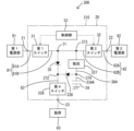
- FIG. 1 is a block diagram illustrating a schematic example of an in-vehicle system including a power supply device according to the first embodiment.
- FIG. 2 is a block diagram illustrating a schematic example of an in-vehicle system including a power supply device according to the second embodiment.
- FIG. 3 is a block diagram illustrating a schematic example of an in-vehicle system including a power supply device according to the third embodiment.
- a power supply device included in an in-vehicle system including a first power supply unit, a second power supply unit, a load, a first conductive path to which power is supplied from the first power supply unit, a second conductive path to which power is supplied from the second power supply unit, and a third conductive path provided between a connection point between the first conductive path and the second conductive path and the load, a first switch provided in the first conductive path; a second switch provided in the second conductive path; a power storage unit that supplies power to the load via the third conductive path; a reverse current prevention unit that prevents a current from flowing from the power storage unit to the first switch via the third conductive path and a current from flowing from the power storage unit to the second switch via the third conductive path;
- a power supply device comprising:
- the first conductive path can be cut off by the first switch. Then, after a power failure of the first power supply unit, power can be supplied from the storage unit to the load via the third conductive path.
- the second conductive path can be cut off by the second switch, and after a power failure, power can be supplied from the storage unit to the load.
- the backflow prevention unit can prevent a current from flowing from the storage unit to the first switch via the third conductive path, and a current from the storage unit to the second switch via the third conductive path. Therefore, the power supply device can realize a configuration that can maintain the power supplied to the load.
- the power supply device of [2] above by providing a backflow prevention unit in the third conductive path, a configuration can be realized that prevents backflow from the storage unit to the first conductive path and the second conductive path. Therefore, the power supply device can have a simpler configuration than when backflow prevention units are provided in both the first conductive path and the second conductive path.
- the power supply device according to any one of [1] to [3], which is configured as a junction box and includes a case member that houses the first switch, the second switch, the power storage unit, and the backflow prevention unit.
- components such as the first switch, the second switch, the power storage unit, and the backflow prevention unit can be consolidated in a junction box, making the device more compact and simplifying the structure.
- a power supply device comprising a fourth conductive path electrically connected to both ends of the reverse current prevention unit and a resistor provided in the fourth conductive path, the fourth conductive path being connected to the third conductive path at a second connection point, the storage unit being electrically connected in the fourth conductive path between the second connection point and the resistor, and a second reverse current prevention unit provided in the fourth conductive path between the second connection point and the storage unit, preventing a current flow from the third conductive path to the storage unit via the second connection point.
- FIG. 1 shows an in-vehicle system 100 including a power supply device 10.
- the in-vehicle system 100 is a system mounted on a vehicle.
- the in-vehicle system 100 includes a first power supply unit 91, a second power supply unit 92, and a load 93.
- the in-vehicle system 100 can supply power from the first power supply unit 91 to the load 93, and can also supply power from the second power supply unit 92 to the load 93.
- the in-vehicle system 100 includes a first conductive path 81, a second conductive path 82, and a third conductive path 83.
- the first conductive path 81 and the second conductive path 82 are provided between a first power supply unit 91 and a second power supply unit 92.
- the first conductive path 81 has one end electrically connected to the first power supply unit 91.
- the second conductive path 82 has one end electrically connected to the second power supply unit 92.
- the other end of the first conductive path 81 and the other end of the second conductive path 82 are electrically connected at a first connection point 71.
- the first connection point 71 corresponds to the "connection point" in this disclosure.
- the third conductive path 83 is provided between the first connection point 71 and a load 93. One end of the third conductive path 83 is electrically connected to the first connection point 71. The other end of the third conductive path 83 is electrically connected to the load 93.
- connection objects preferably means a configuration in which the connection objects are connected in a mutually conductive state (a state in which current can flow) so that the potentials of both connection objects are equal.
- electrically connected may also mean a configuration in which the connection objects are connected in a state in which they can be conductive with an electrical component interposed between them.
- the first conductive path 81 has a first electrical path 81A and a second electrical path 81B.
- the first electrical path 81A constitutes one end side (first power supply unit 91 side) of the first conductive path 81.
- the second electrical path 81B constitutes the other end side (first connection point 71 side) of the first conductive path 81.
- the second conductive path 82 has a third electrical path 82A and a fourth electrical path 82B.
- the third electrical path 82A constitutes one end side (the second power supply unit 92 side) of the second conductive path 82.
- the fourth electrical path 82B constitutes the other end side (the first connection point 71 side) of the second conductive path 82.
- the first power supply unit 91 supplies power to the first conductive path 81.
- the first power supply unit 91 is, for example, a high-voltage battery.
- the first power supply unit 91 may be, for example, a secondary battery such as a lithium-ion battery or a sodium-ion battery, or may be another type of storage battery.
- the high-potential terminal of the first power supply unit 91 is electrically connected to one end of the first conductive path 81.
- the second power supply unit 92 supplies power to the second conductive path 82.
- the second power supply unit 92 is, for example, a low-voltage battery.
- the second power supply unit 92 may be, for example, a secondary battery such as a lithium-ion battery or a lead battery, or may be another type of storage battery.
- the output voltage of the second power supply unit 92 is lower than the output voltage of the first power supply unit 91.
- the high-potential terminal of the second power supply unit 92 is electrically connected to one end of the second conductive path 82.
- the load 93 is, for example, an electrical load used in a vehicle.
- the load 93 is, for example, an electric brake.
- the power supply device 10 is, for example, an electric connection box, more specifically, a junction box.
- the power supply device 10 is electrically connected to a first power supply unit 91, a second power supply unit 92, and a load 93.
- the power supply device 10 has a case member 20, a first terminal 21, a second terminal 22, and a third terminal 23.
- the case member 20 constitutes the outer shell of the power supply device 10.
- the first terminal 21, the second terminal 22, and the third terminal 23 are provided on the case member 20.
- the first terminal 21 is provided between the first power supply unit 91 and a first switch 31 described later (in the middle of the first electrical path 81A).
- the first terminal 21 is electrically connected to the first power supply unit 91 and receives power from the first power supply unit 91.
- the second terminal 22 is provided between the second power supply unit 92 and a second switch 32 described later (in the middle of the third electrical path 82A).
- the second terminal 22 is electrically connected to the second power supply unit 92 and receives power from the second power supply unit 92.
- the third terminal 23 is provided between the load 93 and a second connection point 72 (described later) (in the middle of the third conductive path 83).
- the third terminal 23 is electrically connected to the
- the power supply device 10 has a first switch 31, a second switch 32, and a control unit 33.
- the first switch 31 is provided in the first conductive path 81.
- the first switch 31 is provided between the first electrical path 81A and the second electrical path 81B.
- One end of the first switch 31 is electrically connected to the first electrical path 81A.
- the other end of the first switch 31 is electrically connected to the second electrical path 81B.
- the first switch 31 switches between a first permissive state in which bidirectional current flow is permitted through the first switch 31 and a first blocking state in which current flow from the second electrical path 81B to the first electrical path 81A is blocked.
- the first switch 31 allows current to flow from the first electrical path 81A to the second electrical path 81B when in the first blocking state.
- the first switch 31 includes, for example, a MOSFET.
- the first switch 31 is in the first permissive state when the MOSFET is in the ON state.
- the first switch 31 is in the first blocking state when the MOSFET is in the OFF state.
- the first switch 31 is, for example, an IPD (Intelligent Power Device) that includes a protection circuit, etc.
- the second switch 32 is provided in the second conductive path 82.
- the second switch 32 is provided between the third electrical path 82A and the fourth electrical path 82B.
- One end of the second switch 32 is electrically connected to the third electrical path 82A.
- the other end of the second switch 32 is electrically connected to the fourth electrical path 82B.
- the second switch 32 switches between a second permissive state in which bidirectional current flow is permitted through the second switch 32, and a second blocking state in which current flow from the fourth electrical path 82B to the third electrical path 82A is blocked.
- the second switch 32 allows current to flow from the third electrical path 82A to the fourth electrical path 82B when in the second blocking state.
- the second switch 32 includes, for example, a MOSFET.
- the second switch 32 is in the second permissive state when the MOSFET is in the ON state.
- the second switch 32 is in the second blocking state when the MOSFET is in the OFF state.
- the second switch 32 is, for example, an IPD (Intelligent Power Device) that includes a protection circuit, etc.
- the control unit 33 is an information processing device having information processing functions, calculation functions, control functions, etc.
- the control unit 33 is mainly composed of a microcomputer, for example, and has a calculation device such as a CPU (Central Processing Unit), and a memory such as a ROM (Read Only Memory) or a RAM (Random Access Memory), etc.
- the control unit 33 has a function of transmitting control signals to the first switch 31 and the second switch 32, etc. to control their operation.
- the control unit 33 can supply power to the load 93 from both the first power supply unit 91 and the second power supply unit 92.
- the first switch 31 is in the first permissible state and the second switch 32 is in the second permissible state, it is preferable that power be supplied to the load 93 from the first power supply unit 91.
- the power supply device 10 has an abnormality detection unit (not shown).
- the abnormality detection unit functions to determine whether a ground fault has occurred in the first electrical path 81A or the third electrical path 82A.
- the abnormality detection unit functions to determine whether a ground fault has occurred in the first electrical path 81A or the third electrical path 82A.
- a configuration for determining whether a ground fault has occurred in the third electrical path 82A is shown, but a configuration for determining whether a ground fault has occurred in the first electrical path 81A can also be provided in the same way.
- the abnormality detection unit has, for example, a current detection unit (current sensor) (not shown) provided in the second conductive path 82 (for example, the fourth electrical path 82B).
- the current detection unit detects the magnitude and direction of the current flowing in the second conductive path 82.
- the current detection unit detects the current flowing from the second power supply unit 92 side to the first connection point 71 side, and detects the current flowing from the first connection point 71 side to the second power supply unit 92 side.
- the abnormality detection unit can determine that a ground fault has occurred in the third electrical path 82A.
- the abnormality detection unit may also detect the current flowing from the first connection point 71 to the second power supply unit 92 using the current detection unit, and determine that a ground fault has occurred in the third electrical path 82A if the current value exceeds a threshold current.
- the abnormality detection unit has, for example, a voltage detection unit (voltage detection circuit) (not shown) provided in the second conductive path 82.
- the voltage detection unit detects the voltage of the second conductive path 82 (more specifically, the third electrical path 82A). For example, if a ground fault occurs in the second conductive path 82 when the first switch 31 is in the first permissive state and the second switch 32 is in the second permissive state, a current from the first power supply unit 91 and a current from the second power supply unit 92 flow in the second conductive path 82. If the voltage of the second conductive path 82 falls below a threshold voltage, it can be determined that a ground fault has occurred in the third electrical path 82A.
- the power supply device 10 further includes a power storage unit 34 and a backflow prevention unit 35.
- the case member 20 houses the first switch 31, the second switch 32, the control unit 33, the power storage unit 34, and the backflow prevention unit 35.
- the power storage unit 34 supplies power to the load 93 via the third conductive path 83.
- the power storage unit 34 is configured, for example, by an electric double layer capacitor.
- the power storage unit 34 may be configured, for example, by connecting a plurality of electric double layer capacitors in series.
- One end of the power storage unit 34 is electrically connected to the third conductive path 83.
- the power storage unit 34 is connected to the third conductive path 83 via a conductive path 34A.
- One end of the conductive path 34A is connected to the second connection point 72 in the third conductive path 83.
- the other end of the conductive path 34A is connected to one end of the power storage unit 34.
- the reverse current prevention unit 35 is provided in the third conductive path 83 between the storage unit 34 and the first connection point 71.
- the reverse current prevention unit 35 prevents current flow from the storage unit 34 to the first switch 31 via the third conductive path 83, and current flow from the storage unit 34 to the second switch 32 via the third conductive path 83.
- the reverse current prevention unit 35 is composed of a rectifier diode (e.g., an ideal diode) such as a PN junction diode.
- the anode of the reverse current prevention unit 35 is electrically connected to the first connection point 71.
- a voltage based on the power supply voltage of the first power supply unit 91 and a voltage based on the power supply voltage of the second power supply unit 92 are applied to the anode of the reverse current prevention unit 35.
- the cathode of the reverse current prevention unit 35 is electrically connected to the second connection point 72.
- the control unit 33 switches the first switch 31 from the first cut-off state to the first permissive state, and switches the second switch 32 from the second cut-off state to the second permissive state. This causes power to be supplied from the first power supply unit 91 or the second power supply unit 92 to the load 93.
- the start condition may be, for example, that the start switch of the vehicle is switched from an OFF state to an ON state, or may be another condition.
- the start switch is an ignition switch in the case of a vehicle equipped with an engine, and is a power switch in the case of an electric vehicle.
- the second conductive path can be cut off by the second switch 32.
- power can be supplied from the power storage unit 34 to the load 93 via the third conductive path 83, so that the power supply to the load 93 can be maintained seamlessly.
- the abnormality detection unit power can be supplied from the power storage unit 34 to the load 93 until the second switch 32 is switched from the second permissive state to the second cut-off state.
- the backflow prevention unit 35 can prevent current from flowing from the power storage unit 34 to the first switch 31 via the third conductive path 83, and current from the power storage unit 34 to the second switch 32 via the third conductive path 83. This allows power to be supplied from the power storage unit 34 only to the load 93.
- the control unit 33 may maintain the second switch 32 in the second cut-off state even if current no longer flows from the first connection point 71 to the second power supply unit 92.
- the control unit 33 returns the second switch 32 to the second permissive state if a return condition is satisfied.
- the return condition may be a condition that is met, for example, every time a predetermined time has elapsed.
- the return condition may be that the output voltage of the second power supply unit 92 has become equal to or greater than a return voltage.
- the return condition may be that the temperature of the second switch 32 has become equal to or greater than a return temperature.
- the power supply device 10 can perform the same control as when the third electrical path 82A has a ground fault.
- the first electrical path 81A has a ground fault while the first switch 31 is in the first permissive state and the second switch 32 is in the second permissive state
- a current from the first power supply unit 91 and a current from the second power supply unit 92 flow through the first electrical path 81A.
- a current flows from the first connection point 71 side to the first power supply unit 91 side
- a ground fault is detected by the abnormality detection unit
- the control unit 33 switches the first switch 31 from the first permissive state to the first cut-off state. This cuts off the flow of current from the first connection point 71 side to the first power supply unit 91 side, and power from the second power supply unit 92 is supplied to the load 93.
- the power supply unit 91 after a power failure of the first power supply unit 91, power can be supplied from the power storage unit 34 to the load 93 via the third conductive path 83, so that the power supply to the load 93 can be maintained seamlessly. Specifically, after a ground fault or the like is detected by the abnormality detection unit, power can be supplied from the power storage unit 34 to the load 93 until the first switch 31 is switched from the first permissive state to the first cut-off state. Furthermore, the backflow prevention unit 35 can prevent the flow of current from the power storage unit 34 to the first switch 31 via the third conductive path 83, and the flow of current from the power storage unit 34 to the second switch 32 via the third conductive path 83. This allows the power from the power storage unit 34 to be supplied only to the load 93.
- Example of effect of power supply device 10 In the power supply device 10, when a ground fault or the like occurs on the first power supply unit 91 side of the first switch 31 in the first conductive path 81, causing a power failure of the first power supply unit 91, the first switch 31 can cut off the first conductive path 81. After the power failure of the first power supply unit 91, power can be supplied from the power storage unit 34 to the load 93 via the third conductive path 83, so that the power supply to the load 93 can be maintained. Similarly, in the case of a power failure of the second power supply unit 92, the second switch 32 can cut off the second conductive path 82, so that the power supply from the power storage unit 34 to the load 93 can be maintained after the power failure.
- the backflow prevention unit 35 can prevent the flow of current from the power storage unit 34 to the first switch 31 via the third conductive path 83 and the flow of current from the power storage unit 34 to the second switch 32 via the third conductive path 83. Therefore, the power supply device 10 can realize a configuration capable of maintaining the power supply to the load 93 .
- the backflow prevention unit 35 is provided in the third conductive path 83 between the power storage unit 34 and the first connection point 71.
- the power supply device 10 by providing the backflow prevention unit 35 in the third conductive path 83, a configuration can be realized that prevents backflow from the power storage unit 34 to the first conductive path 81 and the second conductive path 82. Therefore, the power supply device 10 can have a simpler configuration than when the backflow prevention unit 35 is provided in both the first conductive path 81 and the second conductive path 82.
- Second Embodiment A power supply device 210 of the second embodiment differs from the first embodiment in that a third switch 236 is provided in the third conductive path 83.
- the same components as those in the first embodiment are denoted by the same reference numerals, and detailed description thereof will be omitted.
- the in-vehicle system 200 includes a power supply device 210.
- the power supply device 210 further includes a third switch 236.
- the case member 20 houses the first switch 31, the second switch 32, the control unit 33, the power storage unit 34, the backflow prevention unit 35, and the third switch 236.
- the third switch 236 is provided in series with the reverse current prevention unit 35 between the first connection point 71 and the reverse current prevention unit 35 in the third conductive path 83. One end of the third switch 236 is electrically connected to the first connection point 71. The other end of the third switch 236 is electrically connected to the anode of the reverse current prevention unit 35.
- the third switch 236 switches between a third permissive state in which bidirectional current flow is permitted through the third switch 236, and a third blocking state in which current flow from the first connection point 71 side to the reverse current prevention unit 35 side is blocked.
- the third switch 236 includes, for example, a MOSFET.
- the third switch 236 is in the third permissive state when the MOSFET is in the ON state.
- the third switch 236 is in the third blocking state when the MOSFET is in the OFF state.
- the third switch 236 is, for example, an IPD (Intelligent Power Device) with a built-in protection circuit, etc.
- the control unit 33 controls the operation by sending a control signal to the third switch 236.
- the third switch 236 may be configured, for example, as a pair of MOSFETs having parasitic diodes oriented in opposite directions.
- a ground fault in the load 93 can be detected by providing an abnormality detection unit in the third conductive path 83 that has a similar configuration to the abnormality detection unit described above.
- the abnormality detection unit can determine that a ground fault has occurred in the load 93 when the current flowing from the second connection point 72 side to the load 93 side exceeds a threshold current. Also, for example, it can be determined that a ground fault has occurred in the third conductive path 83 when the voltage of the third conductive path 83 becomes equal to or lower than the threshold voltage.
- the control unit 33 switches the third switch 236 from the third permissive state to the third cut-off state. This cuts off the flow of current from the first connection point 71 side to the load 93 side. In this way, by cutting off the third conductive path 83 with the third switch 236, it is possible to prevent an overcurrent from flowing from the first conductive path 81 side and the second conductive path 82 side to the load 93 side in the event of a ground fault in the load 93.
- the first switch 31 is configured to allow current to flow from the first electrical path 81A to the second electrical path 81B when in the first cut-off state, i.e., if the first switch 31 is a MOSFET having a parasitic diode that allows current to flow from the first electrical path 81A to the second electrical path 81B, then by setting the third switch 236 to the third cut-off state, it is possible to prevent dark current from flowing from the first power supply unit 91 or the second power supply unit 92.
- a power supply device 310 of the third embodiment differs from that of the first embodiment in that some components are added.
- the same components as those of the first embodiment are denoted by the same reference numerals, and detailed description thereof will be omitted.
- the in-vehicle system 300 further includes a fourth conductive path 384.
- the fourth conductive path 384 is electrically connected to both ends of the backflow prevention unit 35.
- One end of the fourth conductive path 384 is connected to the second conductive path (fourth electrical path 82B) at the third connection point 373.
- the other end of the fourth conductive path 384 is connected to the third conductive path 83 at the second connection point 372.
- the power supply device 310 further includes a resistor 337, a second backflow prevention unit 338, and a fourth switch 339.
- the case member 20 houses the first switch 31, the second switch 32, the control unit 33, the power storage unit 34, the backflow prevention unit 35, the resistor 337, the second backflow prevention unit 338, and the fourth switch 339.
- the power storage unit 34 is connected to the fourth conductive path 384 via a conductive path 334A.
- One end of the conductive path 334A is connected to a fourth connection point 374 in the fourth conductive path 384.
- the other end of the conductive path 334A is connected to one end of the power storage unit 34.
- the power storage unit 34 is electrically connected in the fourth conductive path 384 between the second connection point 372 and a resistor 337 described below.
- the resistor 337 is provided in the fourth conductive path 384 between the second connection point 372 and the fourth connection point 374. One end of the resistor 337 is electrically connected to the second connection point 372. The other end of the resistor 337 is electrically connected to the fourth connection point 374.
- the second reverse current prevention unit 338 is provided in the fourth conductive path 384 between the second connection point 372 and the power storage unit 34.
- the second reverse current prevention unit 338 prevents current from flowing from the third conductive path 83 to the power storage unit 34 via the second connection point 372.
- the second reverse current prevention unit 338 is composed of a rectifier diode (e.g., an ideal diode) such as a PN junction diode.
- the anode of the second reverse current prevention unit 338 is electrically connected to the fourth connection point 374.
- the cathode of the second reverse current prevention unit 338 is electrically connected to the second connection point 372.
- the resistor 337 is provided in the fourth conductive path 384 electrically connected to both ends of the backflow prevention unit 35, when power supply from at least one of the first power supply unit 91 and the second power supply unit 92 starts, it is possible to prevent a rush current from flowing into the power storage unit 34 from the side opposite the second connection point 372 in the fourth conductive path 384.
- the second backflow prevention unit 338 is provided between the second connection point 372 and the power storage unit 34 in the fourth conductive path 384, it is possible to prevent a rush current from flowing into the power storage unit 34 from the second connection point 372 side in the fourth conductive path 384.
- the fourth switch 339 is provided between the second connection point 372 and the load 93 in the third conductive path 83. One end of the fourth switch 339 is electrically connected to the second connection point 372. The other end of the fourth switch 339 is electrically connected to the load 93. The fourth switch 339 switches between a fourth permissive state in which bidirectional current flow is permitted through the fourth switch 339 and a fourth blocked state in which current flow from the load 93 side to the first connection point 71 side is blocked.
- the fourth switch 339 includes, for example, a MOSFET.
- the fourth switch 339 is in the fourth permissive state when the MOSFET is in the ON state.
- the fourth switch 339 is in the fourth blocked state when the MOSFET is in the OFF state.
- the fourth switch 339 is, for example, an IPD (Intelligent Power Device) with a built-in protection circuit, etc.
- the control unit 33 controls the operation of the fourth switch 339 by sending a control signal to the fourth switch 339.
- the fourth switch 339 may be configured, for example, as a pair of MOSFETs having parasitic diodes oriented in opposite directions.
- the third conductive path 83 with the fourth switch 339 by interrupting the third conductive path 83 with the fourth switch 339, it is possible to prevent current from flowing from at least one of the first power supply unit 91 and the second power supply unit 92 to the load 93 side via the resistor 337 and the second backflow prevention unit 338, and to prevent current from flowing to the load 93 side via the backflow prevention unit 35.
- the third conductive path 83 with the fourth switch 339 it is possible to prevent overcurrent from flowing from the first conductive path 81 side and the second conductive path 82 side to the load 93 side in the event of a ground fault at the load 93.
- the backflow prevention unit 35 is provided in the third conductive path 83.
- the backflow prevention unit 35 may be provided in at least one of the first conductive path 81 and the second conductive path 82.
- the anode of the backflow prevention unit 35 is electrically connected to the first power supply unit 91, and the cathode is electrically connected to the first connection point 71.
- the backflow prevention unit 35 is provided in the second conductive path 82, the anode of the backflow prevention unit 35 is electrically connected to the second power supply unit 92, and the cathode is electrically connected to the first connection point 71.
- the first power supply unit 91 is configured as a battery.
- the first power supply unit 91 may have a battery and a voltage conversion unit.
- the voltage conversion unit is configured, for example, by a DCDC converter.
- the voltage conversion unit steps up or steps down the voltage input from the battery side and outputs it to the first conductive path 81 side.
- the voltage conversion unit also performs a conversion operation of stepping up or steps down the voltage input from the first conductive path 81 side and outputting it to the battery side.
- the first switch 31 is configured to allow current to flow from the first electrical path 81A to the second electrical path 81B when in the first cut-off state.
- the first switch 31 may be configured to also cut off the flow of current from the second electrical path 81B to the first electrical path 81A when in the first cut-off state.
- the first switch 31 may be configured as a pair of MOSFETs in series having parasitic diodes that are oriented in opposite directions (butted together).
- the second switch 32 is configured to allow current to flow from the third electrical path 82A to the fourth electrical path 82B when in the second cut-off state.
- the second switch 32 may be configured to also cut off the flow of current from the fourth electrical path 82B to the third electrical path 82A when in the second cut-off state.
- the second switch 32 may be configured as a pair of MOSFETs having parasitic diodes oriented in opposite directions.
- the first switch 31 and the second switch 32 are configured as MOSFETs. In contrast, the first switch 31 and the second switch 32 may be configured as mechanical switches.
- the reverse current prevention unit 35 is configured as a diode.
- the reverse current prevention unit 35 may be configured as a parasitic diode of a MOSFET provided between the first connection point 71 and the second connection point 72 in the third conductive path 83.
- a conductive path may be provided that branches off from the first conductive path 81 or the second conductive path 82 to supply power to a load other than the load 93.
- one end of the fourth conductive path 384 is connected to the second conductive path 82.
- one end of the fourth conductive path 384 may be connected to the first conductive path 81.
- Power supply device 20 Case member 21: First terminal 22: Second terminal 23: Third terminal 31: First switch 32: Second switch 33: Control unit 34: Power storage unit 34A: Conduction path 35: Backflow prevention unit 71: First connection point (connection point) 72: Second connection point 81: First conductive path 81A: First electrical path 81B: Second electrical path 82: Second conductive path 82A: Third electrical path 82B: Fourth electrical path 83: Third conductive path 91: First power supply unit 92: Second power supply unit 93: Load 100: In-vehicle system 200: In-vehicle system 210: Power supply device 236: Third switch 300: In-vehicle system 310: Power supply device 334A: Conductive path 337: Resistor 338: Second backflow prevention unit 339: Fourth switch 372: Second connection point 373: Third connection point 374: Fourth connection point 384: Fourth conductive path
Landscapes
- Engineering & Computer Science (AREA)
- Power Engineering (AREA)
- Mechanical Engineering (AREA)
- Charge And Discharge Circuits For Batteries Or The Like (AREA)
- Direct Current Feeding And Distribution (AREA)
Abstract
La présente invention concerne un dispositif d'alimentation électrique capable de maintenir l'alimentation électrique d'une charge. Le dispositif d'alimentation électrique (10) comprend : un premier commutateur (31) disposé sur un premier trajet conducteur (81) ; un second commutateur (32) disposé sur un second trajet conducteur (82) ; une unité de stockage d'énergie (34) pour fournir de l'énergie à une charge (93) par l'intermédiaire d'un troisième trajet conducteur (83) ; et une unité de prévention de reflux (35) pour empêcher l'écoulement de courant de l'unité de stockage d'énergie (34) au premier commutateur (31) par l'intermédiaire du troisième trajet conducteur (83) et l'écoulement de courant de l'unité de stockage d'énergie (34) au second commutateur (32) par l'intermédiaire du troisième trajet conducteur (83).
Applications Claiming Priority (2)
| Application Number | Priority Date | Filing Date | Title |
|---|---|---|---|
| JP2023193587A JP2025080442A (ja) | 2023-11-14 | 2023-11-14 | 電力供給装置 |
| JP2023-193587 | 2023-11-14 |
Publications (1)
| Publication Number | Publication Date |
|---|---|
| WO2025105263A1 true WO2025105263A1 (fr) | 2025-05-22 |
Family
ID=95742252
Family Applications (1)
| Application Number | Title | Priority Date | Filing Date |
|---|---|---|---|
| PCT/JP2024/039431 Pending WO2025105263A1 (fr) | 2023-11-14 | 2024-11-06 | Dispositif d'alimentation électrique |
Country Status (2)
| Country | Link |
|---|---|
| JP (1) | JP2025080442A (fr) |
| WO (1) | WO2025105263A1 (fr) |
Citations (8)
| Publication number | Priority date | Publication date | Assignee | Title |
|---|---|---|---|---|
| JP2004338577A (ja) * | 2003-05-16 | 2004-12-02 | Hitachi Ltd | 車両用電力供給装置及び電力供給方法 |
| KR20080002302U (ko) * | 2006-12-27 | 2008-07-02 | 주식회사 유라코퍼레이션 | 도난경보기용 보조전원공급장치 |
| JP2010178500A (ja) * | 2009-01-29 | 2010-08-12 | Nippon Telegr & Teleph Corp <Ntt> | 放電器、放電方法および直流電源システム |
| WO2016111340A1 (fr) * | 2015-01-09 | 2016-07-14 | 株式会社オートネットワーク技術研究所 | Dispositif d'alimentation électrique d'automobile et boîtier électrique |
| JP2017169307A (ja) * | 2016-03-15 | 2017-09-21 | 株式会社オートネットワーク技術研究所 | 電源装置 |
| WO2020008549A1 (fr) * | 2018-07-04 | 2020-01-09 | 東芝三菱電機産業システム株式会社 | Dispositif d'alimentation électrique sans coupure |
| US20210098986A1 (en) * | 2019-09-27 | 2021-04-01 | Aptiv Technologies Limited | Electronic device |
| JP2022171072A (ja) * | 2021-04-30 | 2022-11-11 | 矢崎総業株式会社 | 電源システム |
-
2023
- 2023-11-14 JP JP2023193587A patent/JP2025080442A/ja active Pending
-
2024
- 2024-11-06 WO PCT/JP2024/039431 patent/WO2025105263A1/fr active Pending
Patent Citations (8)
| Publication number | Priority date | Publication date | Assignee | Title |
|---|---|---|---|---|
| JP2004338577A (ja) * | 2003-05-16 | 2004-12-02 | Hitachi Ltd | 車両用電力供給装置及び電力供給方法 |
| KR20080002302U (ko) * | 2006-12-27 | 2008-07-02 | 주식회사 유라코퍼레이션 | 도난경보기용 보조전원공급장치 |
| JP2010178500A (ja) * | 2009-01-29 | 2010-08-12 | Nippon Telegr & Teleph Corp <Ntt> | 放電器、放電方法および直流電源システム |
| WO2016111340A1 (fr) * | 2015-01-09 | 2016-07-14 | 株式会社オートネットワーク技術研究所 | Dispositif d'alimentation électrique d'automobile et boîtier électrique |
| JP2017169307A (ja) * | 2016-03-15 | 2017-09-21 | 株式会社オートネットワーク技術研究所 | 電源装置 |
| WO2020008549A1 (fr) * | 2018-07-04 | 2020-01-09 | 東芝三菱電機産業システム株式会社 | Dispositif d'alimentation électrique sans coupure |
| US20210098986A1 (en) * | 2019-09-27 | 2021-04-01 | Aptiv Technologies Limited | Electronic device |
| JP2022171072A (ja) * | 2021-04-30 | 2022-11-11 | 矢崎総業株式会社 | 電源システム |
Also Published As
| Publication number | Publication date |
|---|---|
| JP2025080442A (ja) | 2025-05-26 |
Similar Documents
| Publication | Publication Date | Title |
|---|---|---|
| JP6610439B2 (ja) | 電源装置 | |
| US6239515B1 (en) | Circuit for the protection of electrical devices | |
| EP1175324B1 (fr) | Frein a architecture de systeme electrique par cable avec sources electriques multiples et protection de circuit | |
| JP7539117B2 (ja) | 蓄電装置及びそれを備える車両 | |
| JP6635304B2 (ja) | リレー装置及び車載システム | |
| CN108604809A (zh) | 继电器装置以及电源装置 | |
| CN104704698B (zh) | 用于多电压电网的保护电路装置 | |
| JP2014007883A (ja) | 回路保護装置 | |
| US20190237988A1 (en) | Relay device and power supply device | |
| JP7613247B2 (ja) | 車載用切替装置 | |
| JP2004338577A (ja) | 車両用電力供給装置及び電力供給方法 | |
| JP7658248B2 (ja) | 地絡検出装置 | |
| JP7578910B2 (ja) | 車載用切替装置 | |
| CN214124811U (zh) | 一种驱动电路 | |
| JP2006340450A (ja) | 電池保護回路 | |
| JP2025080442A (ja) | 電力供給装置 | |
| US20250047090A1 (en) | Fuse Circuit Assembly for An Energy System and Energy System | |
| KR20230011495A (ko) | 차량 온보드 전기 네트워크 스위치, 모터 차량 온보드 전기 네트워크 및 모터 차량 온보드 전기 네트워크 스위치 작동 방법 | |
| US20240275264A1 (en) | Circuit arrangement and electrical system | |
| US11721970B2 (en) | On-board electrical system for a vehicle and process for operating an on-board electrical system | |
| US11626722B2 (en) | On-board power supply system for a vehicle | |
| WO2025234030A1 (fr) | Dispositif de coupure embarqué | |
| WO2024241477A1 (fr) | Dispositif de suppression de surtension | |
| JP2002112470A (ja) | オフラインupsシステム | |
| US20240364131A1 (en) | Power supply system |
Legal Events
| Date | Code | Title | Description |
|---|---|---|---|
| 121 | Ep: the epo has been informed by wipo that ep was designated in this application |
Ref document number: 24891301 Country of ref document: EP Kind code of ref document: A1 |