CN1044526C - 半导体存贮装置 - Google Patents
半导体存贮装置 Download PDFInfo
- Publication number
- CN1044526C CN1044526C CN95100739A CN95100739A CN1044526C CN 1044526 C CN1044526 C CN 1044526C CN 95100739 A CN95100739 A CN 95100739A CN 95100739 A CN95100739 A CN 95100739A CN 1044526 C CN1044526 C CN 1044526C
- Authority
- CN
- China
- Prior art keywords
- word line
- level
- potential
- circuit
- node
- Prior art date
- Legal status (The legal status is an assumption and is not a legal conclusion. Google has not performed a legal analysis and makes no representation as to the accuracy of the status listed.)
- Expired - Lifetime
Links
- 239000004065 semiconductor Substances 0.000 title claims abstract description 38
- 238000006243 chemical reaction Methods 0.000 claims abstract description 73
- 230000015572 biosynthetic process Effects 0.000 claims description 10
- 239000000758 substrate Substances 0.000 claims description 4
- 239000003990 capacitor Substances 0.000 claims description 3
- 230000003071 parasitic effect Effects 0.000 claims description 3
- 238000007599 discharging Methods 0.000 claims 1
- 230000007257 malfunction Effects 0.000 abstract description 7
- 238000010586 diagram Methods 0.000 description 14
- 101100084617 Arabidopsis thaliana PBG1 gene Proteins 0.000 description 13
- 230000000694 effects Effects 0.000 description 13
- 230000009471 action Effects 0.000 description 11
- 230000008859 change Effects 0.000 description 8
- 238000005516 engineering process Methods 0.000 description 8
- 230000009977 dual effect Effects 0.000 description 4
- 239000000203 mixture Substances 0.000 description 3
- 230000008901 benefit Effects 0.000 description 2
- 239000012467 final product Substances 0.000 description 2
- 230000006870 function Effects 0.000 description 2
- 230000002093 peripheral effect Effects 0.000 description 2
- 239000000047 product Substances 0.000 description 2
- 230000002123 temporal effect Effects 0.000 description 2
- 241001269238 Data Species 0.000 description 1
- 230000000295 complement effect Effects 0.000 description 1
- 230000008602 contraction Effects 0.000 description 1
- 238000006880 cross-coupling reaction Methods 0.000 description 1
- 230000008676 import Effects 0.000 description 1
- 238000000034 method Methods 0.000 description 1
Images


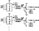

Classifications
-
- G—PHYSICS
- G11—INFORMATION STORAGE
- G11C—STATIC STORES
- G11C11/00—Digital stores characterised by the use of particular electric or magnetic storage elements; Storage elements therefor
- G11C11/21—Digital stores characterised by the use of particular electric or magnetic storage elements; Storage elements therefor using electric elements
- G11C11/34—Digital stores characterised by the use of particular electric or magnetic storage elements; Storage elements therefor using electric elements using semiconductor devices
- G11C11/40—Digital stores characterised by the use of particular electric or magnetic storage elements; Storage elements therefor using electric elements using semiconductor devices using transistors
- G11C11/401—Digital stores characterised by the use of particular electric or magnetic storage elements; Storage elements therefor using electric elements using semiconductor devices using transistors forming cells needing refreshing or charge regeneration, i.e. dynamic cells
- G11C11/4063—Auxiliary circuits, e.g. for addressing, decoding, driving, writing, sensing or timing
- G11C11/407—Auxiliary circuits, e.g. for addressing, decoding, driving, writing, sensing or timing for memory cells of the field-effect type
-
- G—PHYSICS
- G11—INFORMATION STORAGE
- G11C—STATIC STORES
- G11C8/00—Arrangements for selecting an address in a digital store
- G11C8/08—Word line control circuits, e.g. drivers, boosters, pull-up circuits, pull-down circuits, precharging circuits, for word lines
-
- G—PHYSICS
- G11—INFORMATION STORAGE
- G11C—STATIC STORES
- G11C8/00—Arrangements for selecting an address in a digital store
- G11C8/10—Decoders
Landscapes
- Engineering & Computer Science (AREA)
- Microelectronics & Electronic Packaging (AREA)
- Computer Hardware Design (AREA)
- Dram (AREA)
- Static Random-Access Memory (AREA)
- Semiconductor Memories (AREA)
Applications Claiming Priority (4)
| Application Number | Priority Date | Filing Date | Title |
|---|---|---|---|
| JP008921/94 | 1994-01-31 | ||
| JP892194 | 1994-01-31 | ||
| JPP07-008471 | 1995-01-21 | ||
| JP7008471A JPH07254275A (ja) | 1994-01-31 | 1995-01-23 | 半導体記憶装置 |
Publications (2)
| Publication Number | Publication Date |
|---|---|
| CN1117645A CN1117645A (zh) | 1996-02-28 |
| CN1044526C true CN1044526C (zh) | 1999-08-04 |
Family
ID=26342986
Family Applications (1)
| Application Number | Title | Priority Date | Filing Date |
|---|---|---|---|
| CN95100739A Expired - Lifetime CN1044526C (zh) | 1994-01-31 | 1995-01-28 | 半导体存贮装置 |
Country Status (6)
| Country | Link |
|---|---|
| US (7) | US5825714A (fr) |
| EP (5) | EP0665556B1 (fr) |
| JP (1) | JPH07254275A (fr) |
| KR (1) | KR100201723B1 (fr) |
| CN (1) | CN1044526C (fr) |
| DE (4) | DE69526460T2 (fr) |
Families Citing this family (43)
| Publication number | Priority date | Publication date | Assignee | Title |
|---|---|---|---|---|
| JPH07254275A (ja) * | 1994-01-31 | 1995-10-03 | Toshiba Corp | 半導体記憶装置 |
| JP3134798B2 (ja) * | 1996-11-15 | 2001-02-13 | 日本電気株式会社 | 電圧発生回路 |
| KR100234878B1 (ko) * | 1997-01-13 | 1999-12-15 | 윤종용 | 반도체 메모리 장치 |
| JPH10241364A (ja) * | 1997-02-28 | 1998-09-11 | Toshiba Corp | Dram装置及びロジック混載lsi |
| US6009037A (en) * | 1997-09-25 | 1999-12-28 | Texas Instruments Incorporated | Dynamic logic memory addressing circuits, systems, and methods with reduced capacitively loaded predecoders |
| JPH11306751A (ja) * | 1998-04-22 | 1999-11-05 | Toshiba Corp | 半導体記憶装置 |
| US6321296B1 (en) * | 1998-08-04 | 2001-11-20 | International Business Machines Corporation | SDRAM L3 cache using speculative loads with command aborts to lower latency |
| JP4398551B2 (ja) | 1998-12-25 | 2010-01-13 | 株式会社東芝 | 半導体装置 |
| DE69927364D1 (de) * | 1999-07-28 | 2005-10-27 | St Microelectronics Srl | Einzige Speisespannungsschaltung für nichtflüchtigen Speicher mit hierarchischem Reihendekodierer |
| JP3566608B2 (ja) * | 1999-12-28 | 2004-09-15 | Necエレクトロニクス株式会社 | 半導体集積回路 |
| JP3534681B2 (ja) | 2000-06-01 | 2004-06-07 | 松下電器産業株式会社 | 半導体記憶装置 |
| DE10038925A1 (de) * | 2000-08-09 | 2002-03-14 | Infineon Technologies Ag | Elektronische Treiberschaltung für Wortleitungen einer Speichermatrix und Speichervorrichtung |
| JP2002298579A (ja) * | 2001-03-29 | 2002-10-11 | Toshiba Corp | 半導体記憶装置 |
| DE10116358A1 (de) | 2001-04-02 | 2002-11-07 | Micronas Gmbh | Vorrichtung und Verfahren zur Erfassung und Unterdrückung von Störungen |
| US6426914B1 (en) * | 2001-04-20 | 2002-07-30 | International Business Machines Corporation | Floating wordline using a dynamic row decoder and bitline VDD precharge |
| US6597623B2 (en) * | 2001-06-28 | 2003-07-22 | Intel Corporation | Low power architecture for register files |
| KR100477040B1 (ko) * | 2001-09-10 | 2005-03-18 | 가부시끼가이샤 도시바 | 반도체 기억 장치 |
| US6628565B2 (en) * | 2001-11-05 | 2003-09-30 | Micron Technology, Inc. | Predecode column architecture and method |
| US6785186B2 (en) * | 2002-08-21 | 2004-08-31 | Micron Technology, Inc. | Design of an high speed xdecoder driving a large wordline load consuming less switching current for use in high speed syncflash memory |
| JP4439185B2 (ja) * | 2003-02-07 | 2010-03-24 | パナソニック株式会社 | 半導体記憶装置 |
| US7200050B2 (en) * | 2003-05-26 | 2007-04-03 | Semiconductor Energy Laboratory Co., Ltd. | Memory unit and semiconductor device |
| JP2005025907A (ja) * | 2003-07-03 | 2005-01-27 | Hitachi Ltd | 半導体集積回路装置 |
| US7016233B2 (en) * | 2004-05-17 | 2006-03-21 | Taiwan Semiconductor Manufacturing Co., Ltd. | Wordline decoder and memory device |
| KR100634439B1 (ko) * | 2004-10-26 | 2006-10-16 | 삼성전자주식회사 | 퓨즈프리 회로, 퓨즈프리 반도체 집적회로 및 퓨즈프리불휘발성 메모리 장치, 그리고 퓨즈프리 방법 |
| CN100533584C (zh) * | 2004-12-21 | 2009-08-26 | 新唐科技股份有限公司 | 串行只读存储器装置以及存储器系统 |
| US7151711B2 (en) * | 2005-02-23 | 2006-12-19 | United Memories, Inc. | Self-addressed subarray precharge |
| US7355905B2 (en) | 2005-07-01 | 2008-04-08 | P.A. Semi, Inc. | Integrated circuit with separate supply voltage for memory that is different from logic circuit supply voltage |
| US7884645B2 (en) * | 2008-01-31 | 2011-02-08 | Qualcomm Incorporated | Voltage level shifting circuit and method |
| JP2009238323A (ja) * | 2008-03-27 | 2009-10-15 | Fujitsu Microelectronics Ltd | 半導体記憶装置、画像処理システムおよび画像処理方法 |
| US8139426B2 (en) * | 2008-08-15 | 2012-03-20 | Qualcomm Incorporated | Dual power scheme in memory circuit |
| US7924633B2 (en) * | 2009-02-20 | 2011-04-12 | International Business Machines Corporation | Implementing boosted wordline voltage in memories |
| JP4913878B2 (ja) | 2009-05-27 | 2012-04-11 | ルネサスエレクトロニクス株式会社 | ワード線選択回路、ロウデコーダ |
| JP2011034658A (ja) * | 2009-08-06 | 2011-02-17 | Fujitsu Semiconductor Ltd | 半導体記憶装置、ワード線の昇圧方法、及びシステム |
| JP5300709B2 (ja) | 2009-12-14 | 2013-09-25 | 株式会社東芝 | 半導体記憶装置 |
| JP2011198445A (ja) * | 2010-03-24 | 2011-10-06 | Toshiba Corp | 半導体記憶装置 |
| US8737137B1 (en) * | 2013-01-22 | 2014-05-27 | Freescale Semiconductor, Inc. | Flash memory with bias voltage for word line/row driver |
| WO2015162682A1 (fr) * | 2014-04-22 | 2015-10-29 | ユニサンティス エレクトロニクス シンガポール プライベート リミテッド | Dispositif à semi-conducteurs |
| CN104506180A (zh) * | 2014-12-12 | 2015-04-08 | 长沙景嘉微电子股份有限公司 | 一种高速电平转换电路 |
| WO2017019714A1 (fr) * | 2015-07-27 | 2017-02-02 | Power Down Semiconductor Llc | Décodeur de faible puissance utilisant un circuit d'attaque résonant |
| CN113990372B (zh) | 2015-07-27 | 2025-03-18 | 电力荡半导体有限公司 | 采用谐振驱动电路的低功耗sram位单元 |
| US10109365B2 (en) * | 2016-11-28 | 2018-10-23 | Taiwan Semiconductor Manufacturing Company Limited | Word line driver |
| US10658026B2 (en) | 2017-05-26 | 2020-05-19 | Taiwan Semiconductor Manufacturing Company Limited | Word line pulse width control circuit in static random access memory |
| KR20230109003A (ko) * | 2022-01-12 | 2023-07-19 | 에스케이하이닉스 주식회사 | 반도체장치 및 반도체시스템 |
Citations (1)
| Publication number | Priority date | Publication date | Assignee | Title |
|---|---|---|---|---|
| EP0498251A2 (fr) * | 1991-02-05 | 1992-08-12 | International Business Machines Corporation | Circuit d'attaque de ligne de mot pour mémoires dynamiques à accès aléatoire |
Family Cites Families (32)
| Publication number | Priority date | Publication date | Assignee | Title |
|---|---|---|---|---|
| US4344005A (en) * | 1978-07-18 | 1982-08-10 | Rca Corporation | Power gated decoding |
| JPS583325A (ja) * | 1981-06-29 | 1983-01-10 | Fujitsu Ltd | インバ−タ回路 |
| JPS5979488A (ja) * | 1982-10-28 | 1984-05-08 | Nec Corp | Mosメモリ回路 |
| DE3677274D1 (de) * | 1985-07-01 | 1991-03-07 | Nec Corp | Speicherschaltung mit wortzeilenrauschunterdrueckungsschaltungen. |
| US5448517A (en) * | 1987-06-29 | 1995-09-05 | Kabushiki Kaisha Toshiba | Electrically programmable nonvolatile semiconductor memory device with NAND cell structure |
| JPH0821849B2 (ja) * | 1988-10-25 | 1996-03-04 | 富士通株式会社 | 半導体記憶装置 |
| JP2911918B2 (ja) * | 1989-08-30 | 1999-06-28 | 富士通株式会社 | 半導体記憶装置 |
| GB2243233A (en) * | 1990-04-06 | 1991-10-23 | Mosaid Inc | DRAM word line driver |
| JPH0438790A (ja) * | 1990-06-01 | 1992-02-07 | Toshiba Corp | ダイナミック型半導体記憶装置 |
| US5103113A (en) * | 1990-06-13 | 1992-04-07 | Texas Instruments Incorporated | Driving circuit for providing a voltage boasted over the power supply voltage source as a driving signal |
| JPH04106794A (ja) * | 1990-08-27 | 1992-04-08 | Fujitsu Ltd | 半導体記憶装置 |
| JP2564695B2 (ja) * | 1990-09-14 | 1996-12-18 | 富士通株式会社 | 半導体記憶装置 |
| JPH04225182A (ja) * | 1990-12-26 | 1992-08-14 | Toshiba Corp | 半導体記憶装置 |
| JP2829135B2 (ja) * | 1990-12-27 | 1998-11-25 | 株式会社東芝 | 半導体記憶装置 |
| US5202855A (en) * | 1991-01-14 | 1993-04-13 | Motorola, Inc. | DRAM with a controlled boosted voltage level shifting driver |
| JP2835215B2 (ja) * | 1991-07-25 | 1998-12-14 | 株式会社東芝 | 不揮発性半導体記憶装置 |
| KR0113252Y1 (ko) * | 1991-12-24 | 1998-04-14 | 문정환 | 워드라인 전압 공급회로 |
| JPH0817231B2 (ja) * | 1992-01-29 | 1996-02-21 | 東京工業大学長 | 組織ドープ構造半導体装置 |
| JPH0684354A (ja) * | 1992-05-26 | 1994-03-25 | Nec Corp | 行デコーダ回路 |
| KR960006373B1 (ko) * | 1992-10-31 | 1996-05-15 | 삼성전자주식회사 | 반도체 메모리 장치의 워드라인 구동회로 |
| JP3267436B2 (ja) * | 1993-04-19 | 2002-03-18 | 三菱電機株式会社 | 半導体装置 |
| JPH07254275A (ja) * | 1994-01-31 | 1995-10-03 | Toshiba Corp | 半導体記憶装置 |
| JP3080829B2 (ja) * | 1994-02-17 | 2000-08-28 | 株式会社東芝 | カスケード型メモリセル構造を有した多バンクシンクロナスメモリシステム |
| JP3667787B2 (ja) * | 1994-05-11 | 2005-07-06 | 株式会社ルネサステクノロジ | 半導体記憶装置 |
| US5637229A (en) * | 1995-02-17 | 1997-06-10 | Enviroguard, Inc. | Self flocculating separation medium and method |
| US5615164A (en) * | 1995-06-07 | 1997-03-25 | International Business Machines Corporation | Latched row decoder for a random access memory |
| JP3159359B2 (ja) * | 1995-06-22 | 2001-04-23 | 日本電気株式会社 | 半導体装置 |
| JPH09134591A (ja) * | 1995-11-07 | 1997-05-20 | Oki Micro Design Miyazaki:Kk | 半導体メモリ装置 |
| KR0179553B1 (ko) * | 1995-12-29 | 1999-04-15 | 김주용 | 로오 디코더 및 컬럼 디코더 회로 |
| JP3759648B2 (ja) * | 1996-03-04 | 2006-03-29 | 株式会社ルネサステクノロジ | 半導体記憶装置 |
| KR100246311B1 (ko) * | 1996-09-17 | 2000-03-15 | 김영환 | 반도체 메모리소자 |
| US6009023A (en) * | 1998-05-26 | 1999-12-28 | Etron Technology, Inc. | High performance DRAM structure employing multiple thickness gate oxide |
-
1995
- 1995-01-23 JP JP7008471A patent/JPH07254275A/ja not_active Abandoned
- 1995-01-27 US US08/379,290 patent/US5825714A/en not_active Expired - Lifetime
- 1995-01-28 CN CN95100739A patent/CN1044526C/zh not_active Expired - Lifetime
- 1995-01-30 KR KR1019950001885A patent/KR100201723B1/ko not_active Expired - Fee Related
- 1995-01-31 EP EP95101293A patent/EP0665556B1/fr not_active Expired - Lifetime
- 1995-01-31 DE DE69526460T patent/DE69526460T2/de not_active Expired - Lifetime
- 1995-01-31 EP EP95101295A patent/EP0665557B1/fr not_active Expired - Lifetime
- 1995-01-31 EP EP95101292A patent/EP0665555B1/fr not_active Expired - Lifetime
- 1995-01-31 EP EP00101652A patent/EP1005046A3/fr not_active Withdrawn
- 1995-01-31 DE DE69518343T patent/DE69518343T2/de not_active Expired - Lifetime
- 1995-01-31 EP EP99124040A patent/EP0991077B1/fr not_active Expired - Lifetime
- 1995-01-31 DE DE69509931T patent/DE69509931T2/de not_active Expired - Lifetime
- 1995-01-31 DE DE69510834T patent/DE69510834T2/de not_active Expired - Lifetime
-
1996
- 1996-08-14 US US08/696,738 patent/US5793695A/en not_active Expired - Lifetime
-
1997
- 1997-08-06 US US08/907,030 patent/US5838629A/en not_active Expired - Lifetime
-
1998
- 1998-10-09 US US09/168,673 patent/US6044035A/en not_active Expired - Lifetime
-
1999
- 1999-10-25 US US09/425,291 patent/US6141291A/en not_active Expired - Lifetime
- 1999-12-02 US US09/453,086 patent/US6160752A/en not_active Expired - Lifetime
-
2000
- 2000-07-17 US US09/618,163 patent/US6269047B1/en not_active Expired - Fee Related
Patent Citations (2)
| Publication number | Priority date | Publication date | Assignee | Title |
|---|---|---|---|---|
| EP0498251A2 (fr) * | 1991-02-05 | 1992-08-12 | International Business Machines Corporation | Circuit d'attaque de ligne de mot pour mémoires dynamiques à accès aléatoire |
| EP0498251A3 (en) * | 1991-02-05 | 1993-11-24 | Ibm | Word line driver circuit for dynamic random access memories |
Also Published As
| Publication number | Publication date |
|---|---|
| CN1117645A (zh) | 1996-02-28 |
| EP0665555B1 (fr) | 1999-07-21 |
| DE69510834T2 (de) | 1999-12-02 |
| EP0665556A2 (fr) | 1995-08-02 |
| EP0665555A2 (fr) | 1995-08-02 |
| EP0665557A3 (fr) | 1995-10-11 |
| EP0665555A3 (fr) | 1995-10-11 |
| DE69518343D1 (de) | 2000-09-21 |
| EP0991077A2 (fr) | 2000-04-05 |
| KR950024217A (ko) | 1995-08-21 |
| EP1005046A3 (fr) | 2000-07-05 |
| DE69526460D1 (de) | 2002-05-23 |
| DE69509931T2 (de) | 1999-10-28 |
| KR100201723B1 (ko) | 1999-06-15 |
| US6044035A (en) | 2000-03-28 |
| DE69526460T2 (de) | 2002-11-07 |
| US6160752A (en) | 2000-12-12 |
| EP0991077B1 (fr) | 2002-04-17 |
| US5838629A (en) | 1998-11-17 |
| US5825714A (en) | 1998-10-20 |
| JPH07254275A (ja) | 1995-10-03 |
| EP0665556A3 (fr) | 1995-10-11 |
| EP0665556B1 (fr) | 2000-08-16 |
| US6141291A (en) | 2000-10-31 |
| DE69518343T2 (de) | 2001-02-01 |
| EP0665557A2 (fr) | 1995-08-02 |
| DE69510834D1 (de) | 1999-08-26 |
| DE69509931D1 (de) | 1999-07-08 |
| US5793695A (en) | 1998-08-11 |
| EP0665557B1 (fr) | 1999-06-02 |
| US6269047B1 (en) | 2001-07-31 |
| EP1005046A2 (fr) | 2000-05-31 |
| EP0991077A3 (fr) | 2000-07-05 |
Similar Documents
| Publication | Publication Date | Title |
|---|---|---|
| CN1044526C (zh) | 半导体存贮装置 | |
| US8270247B2 (en) | Word line driving circuit and semiconductor storage device | |
| US6545923B2 (en) | Negatively biased word line scheme for a semiconductor memory device | |
| US8022750B2 (en) | Boost circuit | |
| KR100271840B1 (ko) | 회로 면적의 증대를 억제하면서 복수의 전위를 출력할 수 있는내부 전위 발생 회로 | |
| US6456541B2 (en) | Booster circuit for raising voltage by sequentially transferring charges from input terminals of booster units to output terminals thereof in response to clock signals having different phases | |
| US6154387A (en) | Semiconductor memory device utilizing a polarization state of a ferroelectric film | |
| US8717816B2 (en) | Semiconductor memory device | |
| TW578155B (en) | A circuit of boosting a voltage for use in a flash memory device | |
| US7345946B1 (en) | Dual-voltage wordline drive circuit with two stage discharge | |
| CN101620886A (zh) | 用于闪存器件的字线增压器 | |
| US20030111682A1 (en) | Nonvolatile memory and processing system | |
| JP3250525B2 (ja) | 半導体記憶装置 | |
| CN1305073C (zh) | 闪存中的字线译码结构 | |
| CN1695291A (zh) | 半导体集成电路装置 | |
| JP4112824B2 (ja) | 半導体記憶装置 | |
| US6515911B2 (en) | Circuit structure for providing a hierarchical decoding in semiconductor memory devices | |
| US20020159296A1 (en) | High speed decoder for flash memory | |
| JPH10289574A (ja) | 電圧発生回路を有した半導体装置 | |
| US20030043642A1 (en) | Low voltage charge pump apparatus and method | |
| US5737267A (en) | Word line driver circuit | |
| JP4475762B2 (ja) | 階層型列デコーダを有する単一電源電圧不揮発性記憶装置 | |
| US7965561B2 (en) | Row selector occupying a reduced device area for semiconductor memory devices | |
| US6256250B1 (en) | Power supply circuit | |
| JP4243027B2 (ja) | 改良されたワードラインブースト回路 |
Legal Events
| Date | Code | Title | Description |
|---|---|---|---|
| C10 | Entry into substantive examination | ||
| SE01 | Entry into force of request for substantive examination | ||
| C06 | Publication | ||
| PB01 | Publication | ||
| C14 | Grant of patent or utility model | ||
| GR01 | Patent grant | ||
| C17 | Cessation of patent right | ||
| CX01 | Expiry of patent term |
Expiration termination date: 20150128 Granted publication date: 19990804 |