EP0498251A2 - Circuit d'attaque de ligne de mot pour mémoires dynamiques à accès aléatoire - Google Patents
Circuit d'attaque de ligne de mot pour mémoires dynamiques à accès aléatoire Download PDFInfo
- Publication number
- EP0498251A2 EP0498251A2 EP92101270A EP92101270A EP0498251A2 EP 0498251 A2 EP0498251 A2 EP 0498251A2 EP 92101270 A EP92101270 A EP 92101270A EP 92101270 A EP92101270 A EP 92101270A EP 0498251 A2 EP0498251 A2 EP 0498251A2
- Authority
- EP
- European Patent Office
- Prior art keywords
- transistor
- voltage
- wordline
- substrate
- capacitor
- Prior art date
- Legal status (The legal status is an assumption and is not a legal conclusion. Google has not performed a legal analysis and makes no representation as to the accuracy of the status listed.)
- Withdrawn
Links
Images




Classifications
-
- G—PHYSICS
- G11—INFORMATION STORAGE
- G11C—STATIC STORES
- G11C11/00—Digital stores characterised by the use of particular electric or magnetic storage elements; Storage elements therefor
- G11C11/21—Digital stores characterised by the use of particular electric or magnetic storage elements; Storage elements therefor using electric elements
- G11C11/34—Digital stores characterised by the use of particular electric or magnetic storage elements; Storage elements therefor using electric elements using semiconductor devices
- G11C11/40—Digital stores characterised by the use of particular electric or magnetic storage elements; Storage elements therefor using electric elements using semiconductor devices using transistors
- G11C11/401—Digital stores characterised by the use of particular electric or magnetic storage elements; Storage elements therefor using electric elements using semiconductor devices using transistors forming cells needing refreshing or charge regeneration, i.e. dynamic cells
- G11C11/4063—Auxiliary circuits, e.g. for addressing, decoding, driving, writing, sensing or timing
- G11C11/407—Auxiliary circuits, e.g. for addressing, decoding, driving, writing, sensing or timing for memory cells of the field-effect type
- G11C11/408—Address circuits
- G11C11/4085—Word line control circuits, e.g. word line drivers, - boosters, - pull-up, - pull-down, - precharge
-
- G—PHYSICS
- G11—INFORMATION STORAGE
- G11C—STATIC STORES
- G11C11/00—Digital stores characterised by the use of particular electric or magnetic storage elements; Storage elements therefor
- G11C11/21—Digital stores characterised by the use of particular electric or magnetic storage elements; Storage elements therefor using electric elements
- G11C11/34—Digital stores characterised by the use of particular electric or magnetic storage elements; Storage elements therefor using electric elements using semiconductor devices
- G11C11/40—Digital stores characterised by the use of particular electric or magnetic storage elements; Storage elements therefor using electric elements using semiconductor devices using transistors
- G11C11/401—Digital stores characterised by the use of particular electric or magnetic storage elements; Storage elements therefor using electric elements using semiconductor devices using transistors forming cells needing refreshing or charge regeneration, i.e. dynamic cells
- G11C11/4063—Auxiliary circuits, e.g. for addressing, decoding, driving, writing, sensing or timing
- G11C11/407—Auxiliary circuits, e.g. for addressing, decoding, driving, writing, sensing or timing for memory cells of the field-effect type
- G11C11/408—Address circuits
- G11C11/4087—Address decoders, e.g. bit - or word line decoders; Multiple line decoders
Definitions
- the present application relates to dynamic random access memory CMOS integrated circuits. Specifically, a circuit for accessing the word line of an array of memory cells is disclosed, having an improved access time.
- DRAM dynamic random access memory
- the DRAM architecture is typically implemented in CMOS technology, wherein a substrate of P+ material supports an array of storage cells.
- the storage cells typically include a capacitor which is a trench formed in a surface of an N-well formed on a substrate doped to a P+ level. The capacitor trench extends from the surface of the N-well into the P+ substrate.
- each memory cell supports an access transistor which is configured as a PMOS transistor.
- the PMOS transistor has a drain connected to the trench capacitor and a source which constitutes a bit line and input to a relevant sense amplifier.
- Each of the PMOS transistors are formed in an N-well, and all of the N-wells of the access transistors are connected together.
- the foregoing structure provides for high alpha particle immunity because of the N-well.
- One end of the trench capacitor has a direct connection to the heavily doped substrate which is connected to a common ground terminal.
- any noise appearing on the heavily-doped substrate is effectively isolated by the common ground represented by the substrate.
- the memory cells are organized in rows, each row having a common wordline connected to each gate of the gates of all the access transistors of a row.
- the access transistors for all the cells are rendered conductive, connecting the memory cell capacitor to a respective bit line and sense amplifier. Reading of the wordline is inhibited by asserting the voltage potential VDD on the wordline.
- a series of steps are carried out to identify which of the memory cells are to be read. Thereafter the voltage potential is read on the identified memory cell capacitor to determine the logical value represented by voltage stored on the memory cell.
- a logic signal from off the DRAM chip is first decoded and latched defining the wordline of the memory cells for which the data is sought. Once sufficient settling time has elapsed to be certain a complete decode has been effected, the wordline is driven for all the memory cells of a row. Additional time is needed to set the sense amplifier to establish a logic state which corresponds to the memory cell data value. Further steps are then needed to read the sense amplifier logic state and buffer its state to drive an off-chip logic circuit.
- the foregoing time required to access the memory cells of interest may be upwards to 70 nanoseconds. This time limits the DRAM performance and practitioners in the art have concentrated their efforts in reducing the access time.
- the present invention seeks to shorten such access time by greatly improving the speed for driving the wordline to the required voltage for reading a memory cell capacitor. Further, the effort is also directed to maintaining and increasing the signal produced from a memory cell defining either a 1 or 0, thus achieving an improved signal to noise ratio for the sensed logic state, along with an increase in access speed.
- a new DRAM architecture which employs a wordline driver capable of pulling the wordline to a negative potential.
- the wordline is driven by the circuit between a level of VDD, which will maintain the gates of the access transistors at VDD, to a negative potential in which the access transistor will change to a conducting state more rapidly than was previously obtained.
- the wordline driver circuit in accordance with the invention, includes an on-chip negative voltage generator connected to a trench capacitor.
- the trench capacitor is formed in the substrate, and isolated therefrom by a silicon dioxide composite insulator.
- the capacitance of the trench capacitor is set to be several fold times the total wordline capacitance.
- the trench capacitor is maintained at a negative voltage, which may be approximately -1 volts with respect to the substrate.
- the wordline is driven by a series combination of a PMOS pull-up transistor and NMOS pull-down transistor serially connected with the trench capacitor.
- the NMOS transistor conductive channel is formed by a P-well formed within a N-well on the substrate. This effectively isolates the pull-down transistor, and permits the wordline to be pulled to a negative level of -1 volts by selecting a threshold voltage to have a value of approximately VTN + VWLL, where VTN is the threshold voltage of an NMOS transistor built on the P on P+ substrate, and VWLL is the desired wordline pull-down voltage.
- Figure 1 is a schematic diagram of a circuit which is the preferred embodiment of the invention for driving the wordline of a DRAM.
- Figure 2 illustrates the cross-section of the semiconductor topography for implementing an NMOS transistor in a P-well formed in an N-well carried by a P+ substrate.
- Figure 3 illustrates the structure of the trench capacitor used for storage of a charge from the on-chip negative voltage generator.
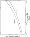
- Figure 4 illustrates the required P-well doping concentration to obtain the threshold voltage for the pull-down NMOS transistor.
- Figure 5 illustrates the pump circuit to generate a negative on-chip voltage.
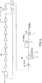
- Figure 6 illustrates the output voltage from the pump circuit as a function of time.
- Figure 7 illustrates a pump regulator circuit for maintaining the negative on-chip voltage to a constant -1 volt.
- FIG. 1 there is shown a circuit in accordance with the preferred embodiment which is capable of driving the wordline of a DRAM to a negative potential with respect to the substrate which is connected to the common ground connection.
- the wordline 10 shown in Figure 1 is connected to a plurality of access transistors, one of which, 19, is shown associated with each single bit memory storage location 11.
- the single bit storage locations are arranged in rows and columns.
- Each storage location includes a trench capacitor 14 formed in the substrate which in CMOS technology, is a P on P+ substrate.
- the trench capacitor 14 is accessed through the PMOS transistor 19, all of which is implemented in CMOS.
- the N-wells of each of the access transistors 19 are connected together and to the substrate, forming an outer N-well which is effectively grounded.
- the sense amplifier 15 includes two switching signal inputs 16 and 17 for setting the sense amplifier 15 in a state to detect the signal from the memory cell capacitor 14.
- An inverter chain 27 is shown which provides the requisite switching signals to 16 and 17 from a sense amplifier set signal generated on chip.
- the reading of the contents of the memory cell 14 occurs as follows: by bringing the wordline from VDDR to a lower potential, the access transistor 19 is enabled. Typically, this PMOS transistor requires a wordline drive voltage of -.8 volts or lower for optimum switching performance. In the prior art, the wordline was pulled to approximately 0 volts, equal to the potential on the substrate, thereby rendering the access transistor 19 conductive. At this time, the particular charge on the cell capacitor 14 representing a 1 or a 0 is applied to the bit line 18. The potential on bit line 18 is compared with a potential on bit line reference 29 by the sense amplifier 15. Depending on the difference between the potential on the cell capacitor 14 and the bit line reference 29, the sense amplifier 15 is set in one of two states.
- the speed at which the access transistor 19 is brought into conduction to permit the contents of the memory capacitor 14 to be read is at least partially dependent upon the potential on the wordline 10. By bringing the wordline 10 to a negative value with respect to the substrate, the speed at which the access transistor 19 is rendered conductive is increased.
- the present invention provides for such negative boosting of the wordline 10 by employing a constant negative voltage generator 26 and trench storage capacitor 25.
- the negative voltage generated on-chip from the generator 26 is stored on a trench capacitor 25 having a capacitance much larger than the wordline 10 capacitance.
- the wordline driver circuit includes a pull-down transistor 24 and pull-up transistor 23.
- the pull-down transistor 24 is shown as an NMOS transistor which is fabricated in a P-well of an N-well on the substrate.
- the pull-up transistor is a PMOS transistor 23 connected to the supply voltage VDDR.
- NMOS transistor 24 Normally, connecting any negative potential to the NMOS transistor 24 would tend to bias the transistor to a conducting condition. Therefore, in the prior art it was not considered practical to establish a negative voltage of -1 to the wordline 10, using the NMOS pull-down transistor 24. As will be evident from Figure 2, an NMOS transistor configured in a P-well, formed in a grounded N-well, permits the source of the NMOS transistor 24 to be returned to a negative voltage.
- Figure 2 illustrates in detail the topography of the NMOS transistor, the P-well 34 within an N-well structure 35 on a P on P+ substrate 33.
- This particular structure will avoid the consequence of connecting the source to a negative potential, wherein the transistor might be biased to a conducting condition holding the wordline at the negative potential.
- the P-well 34 forms the conduction channel for the NMOS transistor, and is at the same voltage as the source of the NMOS device.
- the source of the device is connected to the negative voltage generator.
- the N-well is connected to ground.
- the threshold voltage is established so that VTN + VWLL , where VWLL is the wordline pull-down voltage, and VTN is the threshold voltage of a conventional NMOS device built on a P substrate, which is between .5 and .6 volts. If the wordline pull-down voltage is nominally -1 volt, the preferred threshold for the P-well in N-well NMOS transistor is approximately 1.5 to 1.6 volts. Using a 1.5 to 1.6 volt threshold for the NMOS device permits the decoder stages to be implemented in regular PMOS and NMOS logic, providing the same noise margin to the wordline driver.
- Figure 4 illustrates the P-well doping concentration needed for the P-well in N-well NMOS transistor having conventional CMOS gate thicknesses of 15 nm and 12.5 nm which will obtain the required threshold voltage of 1.5 - 1.6 volts.
- CMOS technology will recognize other techniques such as ion implantation which will also achieve the needed threshold voltage.
- the wordline driver may be switched between a -1 volt potential and VDDR using the pull-up, pull-down combination of PMOS and NMOS transistors of Figure 1 doped according to the table of Figure 4.
- the trench capacitor 25 shown in Figure 1 for accumulating a charge from the negative voltage generator 26 is illustrated in Figure 3.
- the trench capacitor is derived from trenches and diffusion capacitance usurping approximately 90 x 90 sq. um of substrate surface area. This particular structure is smaller than the area of a conduction pad on the integrated circuit and represents a minimal impact on the surface area.
- a silicon dioxide/silicon nitride composite insulator 31, having a thickness of 10 nm is shown formed in the P+ substrate.
- a metal pad 32 is bonded to the top of the trench capacitor to facilitate connection to the negative voltage generator.
- the usual SiO2 surface insulator is shown covering the top portion of the trench capacitor.
- the substrate 33 forms the second terminal of the capacitor.
- the trench capacitor 25 is employed to reduce the change in the output voltage of the negative voltage generator 26.
- the capacitor 25 may be approximately 10 times larger than the wordline capacitance. In a 4 megabyte DRAM chip, a wordline capacitance of approximately 15 pf is experienced, and a trench capacitor of 100 pf will provide the stability to the negative voltage generator 26 output signal.
- VDDR is not greater than VDD.
- the circuit may be necessary where the potential VDDR is reduced from the high logic signal level produced by the decoder 30.
- the circuit may be necessary where the maximum voltage levels on the transistors 22 and 24 may have to be limited due to device reliability requirements.
- the decoder 30 supplies a high logic level greater than VDDR, regulation can be obtained with transistor 20 and transistor 21 such as to reduce the effects of the higher logic signal levels on the wordline pull-up and pull-down transistors 23 and 24.
- FIG. 5 there is shown a pump circuit to generate a negative potential.
- This negative potential is regulated with the pump regulator of Figure 7, producing a regulated potential of -1 volt.
- a ring oscillator comprising a NAND gate 41, a series of inverters 42 and an output buffer amplifier 43.
- the ring oscillator operates when an ENABLE is applied to the X input of NAND gate 41.
- This control signal will be provided by the pump regulator of Figure 7.
- the pump regulator of Figure 7 When the pump regulator of Figure 7 has determined that the capacitor 25 voltage is below a reference voltage, which in the preferred embodiment is -1 volt, NAND gate 41 will be enabled.
- the ring oscillator produces a square wave pulse signal with respect to the ground, i.e., the substrate connection for the DRAM.
- a clamping circuit 44 is shown which receives from the buffer amplifier 43 the square wave pulse signal.
- a first PMOS transistor 45 is connected to operate as a capacitor. In the shown configuration, the source, drain and N-well are all connected to receive the pulsing square wave signal from inverting amplifier 43.
- the PMOS transistor 47 is connected between the gate of PMOS transistor 45 and the capacitor 25.
- the capacitor 25 is connected to the negative going pulse train signal of the output amplifier 43 via the PMOS transistor 45 gate.
- the node K goes positive with respect to the node L, and the PMOS transistor 47 is in a non-conducting condition.
- a PMOS transistor 46 having its source and drain connected together, and its gate and N-well connected to ground, operates as a forward biased diode sinking the positive going signal transitions to ground.
- the net effect of the foregoing clamp circuit is to charge the capacitor 25 negatively with respect to the substrate during negative transitions of the squarewave signal.
- the negative transitions of the squarewave signal from the ring oscillator result in the negative charging of capacitor 25.
- the charge on capacitor 25 leaks somewhat, but retains the majority of the charge received during the negative-going signal excursion.
- a pump regulator provides an enable and disable logic level to the NAND gate 41 of Figure 5.
- This enable signal is developed from a latch 50.
- Latch 50 receives on one reference node 52 a current from the source voltage VDD through a connected PMOS transistor 55.
- a complementary node 51 receives through a PMOS transistor 54 a similar current, under control of a gate signal.
- the gate signal applied to the PMOS transistor 54 is taken from the node L, representing the charging end of the capacitor 25.
- transistor 54 will conduct, as the -1 volt level is exceeded, tending to switch the latch 50 by providing the required imbalance between switching nodes 51 and 52.
- the inverter chain 56 will apply the appropriate logic level signal to NAND gate 41, thus disabling the ring oscillator.
- the ring oscillator will remain in a disabled condition until the latch 50 is switched by detecting a capacitor voltage at node L to be less than -1 volt. At this point, node 52 will be receiving a greater current than node 51 and thereafter the latch 50 switches to enable NAND gate 41.
Landscapes
- Engineering & Computer Science (AREA)
- Microelectronics & Electronic Packaging (AREA)
- Computer Hardware Design (AREA)
- Dram (AREA)
- Semiconductor Memories (AREA)
Applications Claiming Priority (2)
| Application Number | Priority Date | Filing Date | Title |
|---|---|---|---|
| US07/651,070 US5253202A (en) | 1991-02-05 | 1991-02-05 | Word line driver circuit for dynamic random access memories |
| US651070 | 1991-02-05 |
Publications (2)
| Publication Number | Publication Date |
|---|---|
| EP0498251A2 true EP0498251A2 (fr) | 1992-08-12 |
| EP0498251A3 EP0498251A3 (en) | 1993-11-24 |
Family
ID=24611457
Family Applications (1)
| Application Number | Title | Priority Date | Filing Date |
|---|---|---|---|
| EP19920101270 Withdrawn EP0498251A3 (en) | 1991-02-05 | 1992-01-27 | Word line driver circuit for dynamic random access memories |
Country Status (3)
| Country | Link |
|---|---|
| US (1) | US5253202A (fr) |
| EP (1) | EP0498251A3 (fr) |
| JP (1) | JP2516296B2 (fr) |
Cited By (3)
| Publication number | Priority date | Publication date | Assignee | Title |
|---|---|---|---|---|
| WO1996024137A3 (fr) * | 1995-01-31 | 1996-09-26 | Cirrus Logic Inc | Circuits, systemes et procedes permettant d'ameliorer la vitesse de selection des lignes dans un composant memoire a selection de lignes |
| CN1044526C (zh) * | 1994-01-31 | 1999-08-04 | 东芝株式会社 | 半导体存贮装置 |
| WO2007002509A2 (fr) | 2005-06-24 | 2007-01-04 | Monolithic System Technology, Inc. | Dispositif de commande de canal mot pour dram integree dans un processus logique |
Families Citing this family (25)
| Publication number | Priority date | Publication date | Assignee | Title |
|---|---|---|---|---|
| JP3743453B2 (ja) * | 1993-01-27 | 2006-02-08 | セイコーエプソン株式会社 | 不揮発性半導体記憶装置 |
| KR100300622B1 (ko) * | 1993-01-29 | 2001-11-22 | 사와무라 시코 | 반도체 기억장치 |
| JPH08125034A (ja) | 1993-12-03 | 1996-05-17 | Mitsubishi Electric Corp | 半導体記憶装置 |
| JP3667787B2 (ja) * | 1994-05-11 | 2005-07-06 | 株式会社ルネサステクノロジ | 半導体記憶装置 |
| US5724286A (en) * | 1994-12-14 | 1998-03-03 | Mosaid Technologies Incorporated | Flexible DRAM array |
| EP0806045B1 (fr) * | 1995-01-26 | 2001-11-28 | Macronix International Co., Ltd. | Circuit d'attaque en reponse a des adresses decodees de ligne de mots a modes de tensions positive et negative |
| KR0170903B1 (ko) * | 1995-12-08 | 1999-03-30 | 김주용 | 하위 워드 라인 구동 회로 및 이를 이용한 반도체 메모리 장치 |
| US6021083A (en) * | 1997-12-05 | 2000-02-01 | Macronix International Co., Ltd. | Block decoded wordline driver with positive and negative voltage modes |
| IT1306963B1 (it) * | 1999-01-19 | 2001-10-11 | St Microelectronics Srl | Circuito a compensazione capacitativa per la regolazione dellatensione di lettura di riga in memorie non-volatili |
| US6477079B2 (en) * | 1999-05-18 | 2002-11-05 | Kabushiki Kaisha Toshiba | Voltage generator for semiconductor device |
| KR100303364B1 (ko) | 1999-06-29 | 2001-11-01 | 박종섭 | 서브 워드라인 구동 회로 |
| US7023833B1 (en) | 1999-09-10 | 2006-04-04 | Pulse-Link, Inc. | Baseband wireless network for isochronous communication |
| US6944148B1 (en) | 1999-09-10 | 2005-09-13 | Pulse-Link, Inc. | Apparatus and method for managing variable-sized data slots within a time division multiple access frame |
| US6658053B1 (en) * | 1999-09-29 | 2003-12-02 | Pulse-Link, Inc. | Pulse shaping for a baseband wireless transmitter |
| US7088795B1 (en) | 1999-11-03 | 2006-08-08 | Pulse-Link, Inc. | Ultra wide band base band receiver |
| US6952456B1 (en) * | 2000-06-21 | 2005-10-04 | Pulse-Link, Inc. | Ultra wide band transmitter |
| US7397867B2 (en) * | 2000-12-14 | 2008-07-08 | Pulse-Link, Inc. | Mapping radio-frequency spectrum in a communication system |
| US7035246B2 (en) * | 2001-03-13 | 2006-04-25 | Pulse-Link, Inc. | Maintaining a global time reference among a group of networked devices |
| US20030072273A1 (en) * | 2001-09-07 | 2003-04-17 | Aiello G. Roberto | System and method for transmitting data in Ultra Wide Band frequencies in a de-centralized system |
| US6809986B2 (en) * | 2002-08-29 | 2004-10-26 | Micron Technology, Inc. | System and method for negative word line driver circuit |
| US20050238113A1 (en) * | 2004-04-26 | 2005-10-27 | John Santhoff | Hybrid communication method and apparatus |
| JP4942979B2 (ja) * | 2004-11-17 | 2012-05-30 | ルネサスエレクトロニクス株式会社 | 半導体装置 |
| US7656740B2 (en) * | 2007-02-05 | 2010-02-02 | Micron Technology, Inc. | Wordline voltage transfer apparatus, systems, and methods |
| WO2010025556A1 (fr) * | 2008-09-05 | 2010-03-11 | Icera Canada ULC | Architecture d'émetteur passif à sorties commutables pour des applications sans fil |
| JP5216907B2 (ja) * | 2011-12-06 | 2013-06-19 | 株式会社京三製作所 | 周波数変換回路 |
Family Cites Families (14)
| Publication number | Priority date | Publication date | Assignee | Title |
|---|---|---|---|---|
| US3925120A (en) * | 1969-10-27 | 1975-12-09 | Hitachi Ltd | A method for manufacturing a semiconductor device having a buried epitaxial layer |
| US4072868A (en) * | 1976-09-16 | 1978-02-07 | International Business Machines Corporation | FET inverter with isolated substrate load |
| US4124863A (en) * | 1977-04-12 | 1978-11-07 | Harris Corporation | Positively biased substrate IC with thermal oxide guard ring |
| JPS59165449A (ja) * | 1983-03-10 | 1984-09-18 | Toshiba Corp | 半導体記憶装置 |
| GB2148589B (en) * | 1983-10-18 | 1987-04-23 | Standard Telephones Cables Ltd | Improvements in intergrated circuits |
| US4688063A (en) * | 1984-06-29 | 1987-08-18 | International Business Machines Corporation | Dynamic ram cell with MOS trench capacitor in CMOS |
| JPS61294690A (ja) * | 1985-06-21 | 1986-12-25 | Hitachi Ltd | 半導体集積回路装置 |
| US4720739A (en) * | 1985-11-08 | 1988-01-19 | Harris Corporation | Dense, reduced leakage CMOS structure |
| US4901280A (en) * | 1986-07-11 | 1990-02-13 | Texas Instruments Incorporated | Pull-up circuit for high impedance word lines |
| US4825275A (en) * | 1987-05-28 | 1989-04-25 | Texas Instruments Incorporated | Integrated bipolar-CMOS circuit isolation for providing different backgate and substrate bias |
| IT1225608B (it) * | 1988-07-06 | 1990-11-22 | Sgs Thomson Microelectronics | Regolazione della tensione prodotta da un moltiplicatore di tensione. |
| JPH02168494A (ja) * | 1988-12-21 | 1990-06-28 | Nec Corp | 半導体記憶回路 |
| JPH02273393A (ja) * | 1989-04-12 | 1990-11-07 | Mitsubishi Electric Corp | 昇圧信号発生回路 |
| US4954731A (en) * | 1989-04-26 | 1990-09-04 | International Business Machines Corporation | Wordline voltage boosting circuits for complementary MOSFET dynamic memories |
-
1991
- 1991-02-05 US US07/651,070 patent/US5253202A/en not_active Expired - Fee Related
- 1991-11-15 JP JP3328181A patent/JP2516296B2/ja not_active Expired - Lifetime
-
1992
- 1992-01-27 EP EP19920101270 patent/EP0498251A3/en not_active Withdrawn
Cited By (5)
| Publication number | Priority date | Publication date | Assignee | Title |
|---|---|---|---|---|
| CN1044526C (zh) * | 1994-01-31 | 1999-08-04 | 东芝株式会社 | 半导体存贮装置 |
| WO1996024137A3 (fr) * | 1995-01-31 | 1996-09-26 | Cirrus Logic Inc | Circuits, systemes et procedes permettant d'ameliorer la vitesse de selection des lignes dans un composant memoire a selection de lignes |
| WO2007002509A2 (fr) | 2005-06-24 | 2007-01-04 | Monolithic System Technology, Inc. | Dispositif de commande de canal mot pour dram integree dans un processus logique |
| EP1894202A4 (fr) * | 2005-06-24 | 2009-03-25 | Mosys Inc | Dispositif de commande de canal mot pour dram integree dans un processus logique |
| KR101392094B1 (ko) | 2005-06-24 | 2014-05-07 | 인벤사스 코포레이션 | 로직 프로세스의 임베디드 dram을 위한 워드 라인 드라이버 |
Also Published As
| Publication number | Publication date |
|---|---|
| JP2516296B2 (ja) | 1996-07-24 |
| US5253202A (en) | 1993-10-12 |
| EP0498251A3 (en) | 1993-11-24 |
| JPH04278285A (ja) | 1992-10-02 |
Similar Documents
| Publication | Publication Date | Title |
|---|---|---|
| US5253202A (en) | Word line driver circuit for dynamic random access memories | |
| KR100539496B1 (ko) | 전원전압의큰변화에대해유연성을갖는메모리레귤레이터제어방법 | |
| US6954103B2 (en) | Semiconductor device having internal voltage generated stably | |
| US6363029B1 (en) | Semiconductor device incorporating internal power supply for compensating for deviation in operating condition and fabrication process conditions | |
| US4388705A (en) | Semiconductor memory circuit | |
| US6492863B2 (en) | Internal high voltage generation circuit capable of stably generating internal high voltage and circuit element therefor | |
| US6046627A (en) | Semiconductor device capable of operating stably with reduced power consumption | |
| EP0604195B1 (fr) | Amplificateurs de détection dynamiques à deux étages pour réseau de mémoire | |
| US5258950A (en) | Semiconductor memory device | |
| US5010259A (en) | Voltage boosting circuit and operating method thereof | |
| US5075571A (en) | PMOS wordline boost cricuit for DRAM | |
| JPH07130175A (ja) | 半導体記憶装置 | |
| KR950009234B1 (ko) | 반도체 메모리장치의 비트라인 분리클럭 발생장치 | |
| US4397003A (en) | Dynamic random access memory | |
| US5886942A (en) | Word line driver and semiconductor device | |
| US4918663A (en) | Latch-up control for a CMOS memory with a pumped well | |
| US5132575A (en) | Method for providing multi-level potentials at a sense node | |
| US3938109A (en) | High speed ECL compatible MOS-Ram | |
| CA1167962A (fr) | Circuit d'excitation de lignes de memoire a semiconducteur | |
| US5680071A (en) | Tristate voltage boosted integrated circuit | |
| US6452833B2 (en) | Semiconductor memory device | |
| US6100744A (en) | Integrated circuit devices having improved internal voltage generators which reduce timing skew in buffer circuits therein | |
| US5134317A (en) | Booster circuit for a semiconductor memory device | |
| US5777934A (en) | Semiconductor memory device with variable plate voltage generator | |
| US5539701A (en) | Sense circuit for semiconductor memory devices |
Legal Events
| Date | Code | Title | Description |
|---|---|---|---|
| PUAI | Public reference made under article 153(3) epc to a published international application that has entered the european phase |
Free format text: ORIGINAL CODE: 0009012 |
|
| AK | Designated contracting states |
Kind code of ref document: A2 Designated state(s): DE FR GB |
|
| 17P | Request for examination filed |
Effective date: 19921210 |
|
| PUAL | Search report despatched |
Free format text: ORIGINAL CODE: 0009013 |
|
| AK | Designated contracting states |
Kind code of ref document: A3 Designated state(s): DE FR GB |
|
| STAA | Information on the status of an ep patent application or granted ep patent |
Free format text: STATUS: THE APPLICATION HAS BEEN WITHDRAWN |
|
| 18W | Application withdrawn |
Withdrawal date: 19960716 |