CN1087103C - Semiconductor device - Google Patents
Semiconductor device Download PDFInfo
- Publication number
- CN1087103C CN1087103C CN97111732A CN97111732A CN1087103C CN 1087103 C CN1087103 C CN 1087103C CN 97111732 A CN97111732 A CN 97111732A CN 97111732 A CN97111732 A CN 97111732A CN 1087103 C CN1087103 C CN 1087103C
- Authority
- CN
- China
- Prior art keywords
- type
- transistor
- zone
- mos transistor
- diffusion layer
- Prior art date
- Legal status (The legal status is an assumption and is not a legal conclusion. Google has not performed a legal analysis and makes no representation as to the accuracy of the status listed.)
- Expired - Fee Related
Links
Images


Classifications
-
- H—ELECTRICITY
- H10—SEMICONDUCTOR DEVICES; ELECTRIC SOLID-STATE DEVICES NOT OTHERWISE PROVIDED FOR
- H10D—INORGANIC ELECTRIC SEMICONDUCTOR DEVICES
- H10D84/00—Integrated devices formed in or on semiconductor substrates that comprise only semiconducting layers, e.g. on Si wafers or on GaAs-on-Si wafers
- H10D84/80—Integrated devices formed in or on semiconductor substrates that comprise only semiconducting layers, e.g. on Si wafers or on GaAs-on-Si wafers characterised by the integration of at least one component covered by groups H10D12/00 or H10D30/00, e.g. integration of IGFETs
- H10D84/82—Integrated devices formed in or on semiconductor substrates that comprise only semiconducting layers, e.g. on Si wafers or on GaAs-on-Si wafers characterised by the integration of at least one component covered by groups H10D12/00 or H10D30/00, e.g. integration of IGFETs of only field-effect components
-
- H—ELECTRICITY
- H10—SEMICONDUCTOR DEVICES; ELECTRIC SOLID-STATE DEVICES NOT OTHERWISE PROVIDED FOR
- H10D—INORGANIC ELECTRIC SEMICONDUCTOR DEVICES
- H10D89/00—Aspects of integrated devices not covered by groups H10D84/00 - H10D88/00
- H10D89/60—Integrated devices comprising arrangements for electrical or thermal protection, e.g. protection circuits against electrostatic discharge [ESD]
- H10D89/601—Integrated devices comprising arrangements for electrical or thermal protection, e.g. protection circuits against electrostatic discharge [ESD] for devices having insulated gate electrodes, e.g. for IGFETs or IGBTs
- H10D89/811—Integrated devices comprising arrangements for electrical or thermal protection, e.g. protection circuits against electrostatic discharge [ESD] for devices having insulated gate electrodes, e.g. for IGFETs or IGBTs using FETs as protective elements
-
- H—ELECTRICITY
- H02—GENERATION; CONVERSION OR DISTRIBUTION OF ELECTRIC POWER
- H02H—EMERGENCY PROTECTIVE CIRCUIT ARRANGEMENTS
- H02H9/00—Emergency protective circuit arrangements for limiting excess current or voltage without disconnection
- H02H9/04—Emergency protective circuit arrangements for limiting excess current or voltage without disconnection responsive to excess voltage
- H02H9/045—Emergency protective circuit arrangements for limiting excess current or voltage without disconnection responsive to excess voltage adapted to a particular application and not provided for elsewhere
- H02H9/046—Emergency protective circuit arrangements for limiting excess current or voltage without disconnection responsive to excess voltage adapted to a particular application and not provided for elsewhere responsive to excess voltage appearing at terminals of integrated circuits
Landscapes
- Semiconductor Integrated Circuits (AREA)
- Metal-Oxide And Bipolar Metal-Oxide Semiconductor Integrated Circuits (AREA)
- Insulated Gate Type Field-Effect Transistor (AREA)
Abstract
本发明的目的是要提供一种对外来过电压具有高的保护性能的半导体装置。该装置在其模拟开关30中具有一个其漏极端子连接于一个P型传输门4的外侧中的P型扩散层,并且其栅极和源极端子连接于电源电位的P型虚拟晶体管11,和一个其漏极端子连接于一个N型传输门5的外侧中的N型扩散层,并且其栅极和源极端子连接于接地电位的N型虚拟晶体管12,并且当从外部施加一个过电压时,使得过电流经过P型和N型虚拟晶体管11和12流向电源电位或接地电位。
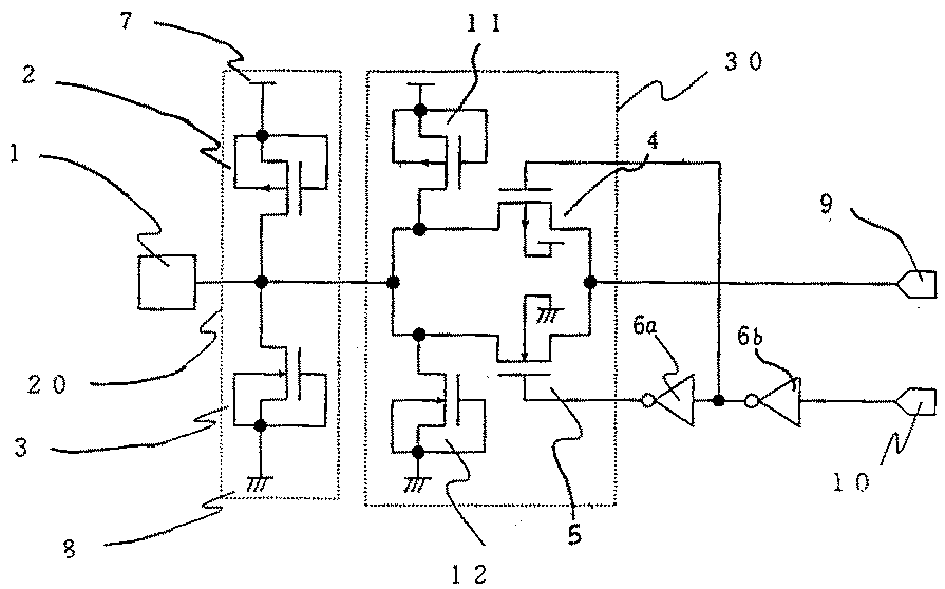
SUMMARY OF THE INVENTION An object of the present invention is to provide a semiconductor device having high protection performance against external overvoltage. The device has in its analog switch 30 a P-type dummy transistor 11 whose drain terminal is connected to a P-type diffusion layer in the outside of a P-type transmission gate 4, and whose gate and source terminals are connected to the supply potential, and an N-type dummy transistor 12 whose drain terminal is connected to an N-type diffusion layer in the outer side of an N-type transmission gate 5, and whose gate and source terminals are connected to ground potential, and when an overvoltage is applied from the outside , causing overcurrent to flow to the power supply potential or the ground potential through the P-type and N-type dummy transistors 11 and 12 .
Description
Claims (9)
Applications Claiming Priority (3)
| Application Number | Priority Date | Filing Date | Title |
|---|---|---|---|
| JP103037 | 1996-04-25 | ||
| JP103037/96 | 1996-04-25 | ||
| JP8103037A JP2914292B2 (en) | 1996-04-25 | 1996-04-25 | Semiconductor device |
Publications (2)
| Publication Number | Publication Date |
|---|---|
| CN1175091A CN1175091A (en) | 1998-03-04 |
| CN1087103C true CN1087103C (en) | 2002-07-03 |
Family
ID=14343473
Family Applications (1)
| Application Number | Title | Priority Date | Filing Date |
|---|---|---|---|
| CN97111732A Expired - Fee Related CN1087103C (en) | 1996-04-25 | 1997-04-24 | Semiconductor device |
Country Status (5)
| Country | Link |
|---|---|
| US (1) | US5905287A (en) |
| EP (1) | EP0803908A3 (en) |
| JP (1) | JP2914292B2 (en) |
| KR (1) | KR100249716B1 (en) |
| CN (1) | CN1087103C (en) |
Families Citing this family (30)
| Publication number | Priority date | Publication date | Assignee | Title |
|---|---|---|---|---|
| US6097066A (en) * | 1997-10-06 | 2000-08-01 | Taiwan Semiconductor Manufacturing Co., Ltd. | Electro-static discharge protection structure for semiconductor devices |
| JP3430080B2 (en) * | 1999-10-08 | 2003-07-28 | Necエレクトロニクス株式会社 | Semiconductor device and manufacturing method thereof |
| JP3495031B2 (en) * | 2002-05-28 | 2004-02-09 | 沖電気工業株式会社 | ESD protection circuit for semiconductor devices |
| US7179691B1 (en) | 2002-07-29 | 2007-02-20 | Taiwan Semiconductor Manufacturing Co., Ltd. | Method for four direction low capacitance ESD protection |
| US6798022B1 (en) * | 2003-03-11 | 2004-09-28 | Oki Electric Industry Co., Ltd. | Semiconductor device with improved protection from electrostatic discharge |
| US7908578B2 (en) * | 2007-08-02 | 2011-03-15 | Tela Innovations, Inc. | Methods for designing semiconductor device with dynamic array section |
| US8653857B2 (en) | 2006-03-09 | 2014-02-18 | Tela Innovations, Inc. | Circuitry and layouts for XOR and XNOR logic |
| US8658542B2 (en) | 2006-03-09 | 2014-02-25 | Tela Innovations, Inc. | Coarse grid design methods and structures |
| US7446352B2 (en) | 2006-03-09 | 2008-11-04 | Tela Innovations, Inc. | Dynamic array architecture |
| US8448102B2 (en) | 2006-03-09 | 2013-05-21 | Tela Innovations, Inc. | Optimizing layout of irregular structures in regular layout context |
| US7956421B2 (en) | 2008-03-13 | 2011-06-07 | Tela Innovations, Inc. | Cross-coupled transistor layouts in restricted gate level layout architecture |
| US8839175B2 (en) | 2006-03-09 | 2014-09-16 | Tela Innovations, Inc. | Scalable meta-data objects |
| US9563733B2 (en) | 2009-05-06 | 2017-02-07 | Tela Innovations, Inc. | Cell circuit and layout with linear finfet structures |
| US8541879B2 (en) | 2007-12-13 | 2013-09-24 | Tela Innovations, Inc. | Super-self-aligned contacts and method for making the same |
| US7763534B2 (en) | 2007-10-26 | 2010-07-27 | Tela Innovations, Inc. | Methods, structures and designs for self-aligning local interconnects used in integrated circuits |
| US9230910B2 (en) | 2006-03-09 | 2016-01-05 | Tela Innovations, Inc. | Oversized contacts and vias in layout defined by linearly constrained topology |
| TWI296150B (en) * | 2006-04-25 | 2008-04-21 | Siliconmotion Inc | An analog input/output circuit with esd protection |
| JP5241109B2 (en) * | 2007-02-01 | 2013-07-17 | ルネサスエレクトロニクス株式会社 | Semiconductor integrated circuit device |
| US8667443B2 (en) | 2007-03-05 | 2014-03-04 | Tela Innovations, Inc. | Integrated circuit cell library for multiple patterning |
| US8453094B2 (en) | 2008-01-31 | 2013-05-28 | Tela Innovations, Inc. | Enforcement of semiconductor structure regularity for localized transistors and interconnect |
| US7939443B2 (en) | 2008-03-27 | 2011-05-10 | Tela Innovations, Inc. | Methods for multi-wire routing and apparatus implementing same |
| KR101761530B1 (en) | 2008-07-16 | 2017-07-25 | 텔라 이노베이션스, 인코포레이티드 | Methods for cell phasing and placement in dynamic array architecture and implementation of the same |
| US8661392B2 (en) | 2009-10-13 | 2014-02-25 | Tela Innovations, Inc. | Methods for cell boundary encroachment and layouts implementing the Same |
| US9159627B2 (en) | 2010-11-12 | 2015-10-13 | Tela Innovations, Inc. | Methods for linewidth modification and apparatus implementing the same |
| CN102569400B (en) * | 2011-12-13 | 2014-11-05 | 钜泉光电科技(上海)股份有限公司 | Metal-oxide-semiconductor device |
| US9613952B2 (en) * | 2014-07-25 | 2017-04-04 | Macronix International Co., Ltd. | Semiconductor ESD protection device |
| CN105846804A (en) * | 2016-03-24 | 2016-08-10 | 天津理工大学 | High-voltage measurement switching circuit based on multipath gating |
| CN106961215B (en) * | 2017-05-12 | 2019-01-22 | 金戈 | A kind of non-anti-Buck-boost transformation chip of high efficiency with instantaneous correction function |
| US10692808B2 (en) | 2017-09-18 | 2020-06-23 | Qualcomm Incorporated | High performance cell design in a technology with high density metal routing |
| TWI894425B (en) * | 2022-01-18 | 2025-08-21 | 聯華電子股份有限公司 | Semiconductor structure with backside through silicon vias and method of obtaining die ids thereof |
Citations (1)
| Publication number | Priority date | Publication date | Assignee | Title |
|---|---|---|---|---|
| EP0248608A1 (en) * | 1986-06-03 | 1987-12-09 | Sony Corporation | Output buffer circuits |
Family Cites Families (15)
| Publication number | Priority date | Publication date | Assignee | Title |
|---|---|---|---|---|
| US4609931A (en) * | 1981-07-17 | 1986-09-02 | Tokyo Shibaura Denki Kabushiki Kaisha | Input protection MOS semiconductor device with zener breakdown mechanism |
| JP2598446B2 (en) * | 1988-01-21 | 1997-04-09 | パイオニア株式会社 | MIS-FET |
| JPH01236731A (en) * | 1988-03-16 | 1989-09-21 | Nec Corp | Complementary analog switch |
| JPH024011A (en) * | 1988-06-21 | 1990-01-09 | Nec Corp | Analog switch circuit |
| JPH0282570A (en) * | 1988-09-19 | 1990-03-23 | Nec Corp | semiconductor equipment |
| JP2633746B2 (en) * | 1991-05-27 | 1997-07-23 | 株式会社東芝 | Semiconductor device |
| JPH05326865A (en) * | 1992-05-14 | 1993-12-10 | Nec Corp | Semiconductor integrated circuit |
| JPH0661439A (en) * | 1992-05-18 | 1994-03-04 | Nec Corp | Semiconductor integrated circuit device |
| JPH07122650A (en) * | 1993-10-22 | 1995-05-12 | Yamaha Corp | Semiconductor device |
| JPH07161926A (en) * | 1993-12-02 | 1995-06-23 | Mitsubishi Electric Corp | Analog signal switching circuit |
| JP3447372B2 (en) * | 1994-06-13 | 2003-09-16 | 富士通株式会社 | Semiconductor device |
| JPH0823269A (en) * | 1994-07-06 | 1996-01-23 | Toshiba Corp | Analog switch circuit |
| JPH0837284A (en) * | 1994-07-21 | 1996-02-06 | Nippondenso Co Ltd | Semiconductor integrated circuit device |
| JPH0837238A (en) * | 1994-07-21 | 1996-02-06 | Hitachi Ltd | Semiconductor integrated circuit device |
| US5714784A (en) * | 1995-10-19 | 1998-02-03 | Winbond Electronics Corporation | Electrostatic discharge protection device |
-
1996
- 1996-04-25 JP JP8103037A patent/JP2914292B2/en not_active Expired - Fee Related
-
1997
- 1997-04-17 US US08/837,344 patent/US5905287A/en not_active Expired - Fee Related
- 1997-04-18 EP EP97106484A patent/EP0803908A3/en not_active Withdrawn
- 1997-04-24 CN CN97111732A patent/CN1087103C/en not_active Expired - Fee Related
- 1997-04-25 KR KR1019970015689A patent/KR100249716B1/en not_active Expired - Fee Related
Patent Citations (1)
| Publication number | Priority date | Publication date | Assignee | Title |
|---|---|---|---|---|
| EP0248608A1 (en) * | 1986-06-03 | 1987-12-09 | Sony Corporation | Output buffer circuits |
Also Published As
| Publication number | Publication date |
|---|---|
| KR100249716B1 (en) | 2000-03-15 |
| JP2914292B2 (en) | 1999-06-28 |
| KR970072397A (en) | 1997-11-07 |
| US5905287A (en) | 1999-05-18 |
| EP0803908A3 (en) | 2000-02-16 |
| JPH09293832A (en) | 1997-11-11 |
| EP0803908A2 (en) | 1997-10-29 |
| CN1175091A (en) | 1998-03-04 |
Similar Documents
| Publication | Publication Date | Title |
|---|---|---|
| CN1087103C (en) | Semiconductor device | |
| JP3161508B2 (en) | Semiconductor device | |
| JP6337634B2 (en) | Semiconductor integrated circuit device | |
| CN107871735B (en) | Semiconductor electrostatic protection circuit device | |
| JP5190913B2 (en) | Semiconductor integrated circuit device | |
| CN1360347A (en) | Electrostatic discharge protection circuit | |
| CN1607664A (en) | Integrated circuit device with electrostatic discharge protection element | |
| US8779516B2 (en) | Semiconductor device | |
| CN1630078A (en) | Semiconductor device | |
| US9722019B2 (en) | High voltage integrated circuit device | |
| CN1396662A (en) | Low voltage trigger silicon controlled rectifier with silicon insulating layer and electrostatic discharge protection circuit | |
| JP4676125B2 (en) | Trench gate type insulated gate bipolar transistor | |
| JP2006100532A (en) | ESD protection circuit | |
| CN1741269A (en) | Substrate-triggered ESD protection circuit using triple well structure | |
| CN105655325A (en) | Electrostatic discharge protection circuit, structure and manufacturing method thereof | |
| WO2012176347A1 (en) | High-voltage integrated circuit device | |
| CN1426108A (en) | Static discharge protective circuit and method in integrated circuit | |
| JPWO2012124677A1 (en) | High voltage integrated circuit device | |
| CN101064305A (en) | Semiconductor device and method for manufacturing the same | |
| CN108987385B (en) | Semiconductor integrated circuit device including electrostatic discharge protection circuit | |
| CN1404149A (en) | Semiconductor device with electrostatic discharge protective circuit | |
| CN1914731A (en) | Buffer circuit having electrostatic discharge protection | |
| CN1901192A (en) | High-voltage electrostatic discharge protection device and manufacturing method thereof | |
| CN1667826A (en) | Input/output cell with robust electrostatic discharge protection | |
| CN1130771C (en) | Semiconductor integrated circuit |
Legal Events
| Date | Code | Title | Description |
|---|---|---|---|
| C10 | Entry into substantive examination | ||
| SE01 | Entry into force of request for substantive examination | ||
| C06 | Publication | ||
| PB01 | Publication | ||
| C14 | Grant of patent or utility model | ||
| GR01 | Patent grant | ||
| ASS | Succession or assignment of patent right |
Owner name: NEC ELECTRONICS TAIWAN LTD. Free format text: FORMER OWNER: NIPPON ELECTRIC CO., LTD. Effective date: 20030411 |
|
| C41 | Transfer of patent application or patent right or utility model | ||
| TR01 | Transfer of patent right |
Effective date of registration: 20030411 Address after: Kanagawa, Japan Patentee after: NEC Corp. Address before: Tokyo, Japan Patentee before: NEC Corp. |
|
| C56 | Change in the name or address of the patentee |
Owner name: RENESAS ELECTRONICS CO., LTD. Free format text: FORMER NAME: NEC CORP. |
|
| CP01 | Change in the name or title of a patent holder |
Address after: Kanagawa, Japan Patentee after: Renesas Electronics Corporation Address before: Kanagawa, Japan Patentee before: NEC Corp. |
|
| C17 | Cessation of patent right | ||
| CF01 | Termination of patent right due to non-payment of annual fee |
Granted publication date: 20020703 Termination date: 20140424 |