CN1187802C - Method for manufacturing thin film transistor containing crystallization silicon active layer - Google Patents
Method for manufacturing thin film transistor containing crystallization silicon active layer Download PDFInfo
- Publication number
- CN1187802C CN1187802C CNB011415770A CN01141577A CN1187802C CN 1187802 C CN1187802 C CN 1187802C CN B011415770 A CNB011415770 A CN B011415770A CN 01141577 A CN01141577 A CN 01141577A CN 1187802 C CN1187802 C CN 1187802C
- Authority
- CN
- China
- Prior art keywords
- active layer
- gate electrode
- metal
- layer
- photoresist
- Prior art date
- Legal status (The legal status is an assumption and is not a legal conclusion. Google has not performed a legal analysis and makes no representation as to the accuracy of the status listed.)
- Expired - Fee Related
Links
Images









Classifications
-
- H—ELECTRICITY
- H10—SEMICONDUCTOR DEVICES; ELECTRIC SOLID-STATE DEVICES NOT OTHERWISE PROVIDED FOR
- H10D—INORGANIC ELECTRIC SEMICONDUCTOR DEVICES
- H10D30/00—Field-effect transistors [FET]
- H10D30/01—Manufacture or treatment
- H10D30/021—Manufacture or treatment of FETs having insulated gates [IGFET]
- H10D30/031—Manufacture or treatment of FETs having insulated gates [IGFET] of thin-film transistors [TFT]
- H10D30/0312—Manufacture or treatment of FETs having insulated gates [IGFET] of thin-film transistors [TFT] characterised by the gate electrodes
- H10D30/0314—Manufacture or treatment of FETs having insulated gates [IGFET] of thin-film transistors [TFT] characterised by the gate electrodes of lateral top-gate TFTs comprising only a single gate
-
- H—ELECTRICITY
- H10—SEMICONDUCTOR DEVICES; ELECTRIC SOLID-STATE DEVICES NOT OTHERWISE PROVIDED FOR
- H10P—GENERIC PROCESSES OR APPARATUS FOR THE MANUFACTURE OR TREATMENT OF DEVICES COVERED BY CLASS H10
- H10P10/00—Bonding of wafers, substrates or parts of devices
-
- H—ELECTRICITY
- H10—SEMICONDUCTOR DEVICES; ELECTRIC SOLID-STATE DEVICES NOT OTHERWISE PROVIDED FOR
- H10D—INORGANIC ELECTRIC SEMICONDUCTOR DEVICES
- H10D30/00—Field-effect transistors [FET]
- H10D30/01—Manufacture or treatment
- H10D30/021—Manufacture or treatment of FETs having insulated gates [IGFET]
- H10D30/031—Manufacture or treatment of FETs having insulated gates [IGFET] of thin-film transistors [TFT]
- H10D30/0321—Manufacture or treatment of FETs having insulated gates [IGFET] of thin-film transistors [TFT] comprising silicon, e.g. amorphous silicon or polysilicon
-
- H—ELECTRICITY
- H10—SEMICONDUCTOR DEVICES; ELECTRIC SOLID-STATE DEVICES NOT OTHERWISE PROVIDED FOR
- H10D—INORGANIC ELECTRIC SEMICONDUCTOR DEVICES
- H10D30/00—Field-effect transistors [FET]
- H10D30/60—Insulated-gate field-effect transistors [IGFET]
- H10D30/67—Thin-film transistors [TFT]
- H10D30/6704—Thin-film transistors [TFT] having supplementary regions or layers in the thin films or in the insulated bulk substrates for controlling properties of the device
- H10D30/6706—Thin-film transistors [TFT] having supplementary regions or layers in the thin films or in the insulated bulk substrates for controlling properties of the device for preventing leakage current
-
- H—ELECTRICITY
- H10—SEMICONDUCTOR DEVICES; ELECTRIC SOLID-STATE DEVICES NOT OTHERWISE PROVIDED FOR
- H10D—INORGANIC ELECTRIC SEMICONDUCTOR DEVICES
- H10D30/00—Field-effect transistors [FET]
- H10D30/60—Insulated-gate field-effect transistors [IGFET]
- H10D30/67—Thin-film transistors [TFT]
- H10D30/6704—Thin-film transistors [TFT] having supplementary regions or layers in the thin films or in the insulated bulk substrates for controlling properties of the device
- H10D30/6713—Thin-film transistors [TFT] having supplementary regions or layers in the thin films or in the insulated bulk substrates for controlling properties of the device characterised by the properties of the source or drain regions, e.g. compositions or sectional shapes
- H10D30/6715—Thin-film transistors [TFT] having supplementary regions or layers in the thin films or in the insulated bulk substrates for controlling properties of the device characterised by the properties of the source or drain regions, e.g. compositions or sectional shapes characterised by the doping profiles, e.g. having lightly-doped source or drain extensions
-
- H—ELECTRICITY
- H10—SEMICONDUCTOR DEVICES; ELECTRIC SOLID-STATE DEVICES NOT OTHERWISE PROVIDED FOR
- H10D—INORGANIC ELECTRIC SEMICONDUCTOR DEVICES
- H10D86/00—Integrated devices formed in or on insulating or conducting substrates, e.g. formed in silicon-on-insulator [SOI] substrates or on stainless steel or glass substrates
Landscapes
- Thin Film Transistor (AREA)
- Recrystallisation Techniques (AREA)
Abstract
本发明揭示了一个制造含结晶硅有源层薄膜晶体管(TFT)的方法,其中诱发有源层结晶的金属从门电极得到补偿,使用掩膜以在有源层中形成轻掺杂漏(LDD)区或者补偿结区。TFT包含金属诱发结晶的硅有源层,LDD区或在沟道区附近形成的补偿结区。该制造TFT的方法不需要附加光刻胶层的形成步骤来形成金属补偿结区,它通过在金属补偿结区低浓度掺杂形成LDD区。因此,按本发明制造的晶体管在关态有低的漏电流和在开态有稳定的电气特性。

The present invention discloses a method of fabricating a thin film transistor (TFT) containing a crystalline silicon active layer, wherein the metal inducing the crystallization of the active layer is compensated from the gate electrode, and a mask is used to form a lightly doped drain (LDD) in the active layer ) area or compensation junction area. The TFT includes a metal-induced crystallization silicon active layer, an LDD region or a compensation junction region formed near the channel region. The method for manufacturing TFT does not require an additional step of forming a photoresist layer to form a metal compensation junction region, and forms an LDD region by low-concentration doping in the metal compensation junction region. Therefore, transistors manufactured according to the present invention have low leakage current in the off state and stable electrical characteristics in the on state.
Description
所属领域Field
本发明与用于液晶显示(LCD)和有机发光管(OLED)等的薄膜晶体管(TFT)相关,特别是与含源区、漏区和沟道区的结晶硅有源层的TFT相关,以及与含结晶硅有源层TFT的制造方法相关。The present invention relates to thin film transistors (TFTs) used in liquid crystal displays (LCDs) and organic light emitting tubes (OLEDs), etc., particularly TFTs with crystalline silicon active layers comprising source, drain and channel regions, and It is related to the manufacturing method of TFT containing crystalline silicon active layer.
背景技术Background technique
用于显示装置,例如液晶显示(LCD)和有机发光管(OLED)等的薄膜晶体管(TFT)是先在透明衬底上,例如玻璃或者石英,沉积一硅层,接着在硅层上制作门和门电极,在硅层的源和漏区注入杂质,退火激活杂质,最后在其上制作绝缘层而成的。TFT的包含源、漏和沟道区的有源层是利用化学汽相沉积(CVD)法等,在如玻璃等透明底面上沉积硅层形成的。经过CVD直接在底面上沉积的硅层是电子迁移率很低的无定形硅层,作为使用薄膜晶体管的显示器件要求高运作速度和小型化结构,其驱动集成电路的集成度越高,其像素区的孔比率就越小。因此,为了使驱动电流与像素TFT一致和提高像素孔比率,要增加硅层的电子迁移率。为此,通过热处理使无定形硅层结晶形成多晶硅来得到高电子迁移率的技术已如下面描述的那样得到了使用。Thin-film transistors (TFTs) used in display devices, such as liquid crystal displays (LCDs) and organic light-emitting tubes (OLEDs), deposit a silicon layer on a transparent substrate, such as glass or quartz, and then make gates on the silicon layer. And the gate electrode, implanting impurities in the source and drain regions of the silicon layer, annealing to activate the impurities, and finally making an insulating layer on it. The active layer of the TFT including the source, drain and channel regions is formed by depositing a silicon layer on a transparent bottom surface such as glass by chemical vapor deposition (CVD) or the like. The silicon layer deposited directly on the bottom surface by CVD is an amorphous silicon layer with very low electron mobility. As a display device using a thin film transistor, it requires high operating speed and a miniaturized structure. The higher the integration of the driver integrated circuit, the higher the pixel The hole ratio of the area is smaller. Therefore, in order to make the driving current consistent with the pixel TFT and improve the pixel hole ratio, the electron mobility of the silicon layer is increased. For this reason, a technique of crystallizing an amorphous silicon layer to form polysilicon by heat treatment to obtain high electron mobility has been used as described below.
固相结晶(SPC)技术用在600℃或低于600℃的温度下,对无定形硅层退火几小时或几十小时,600℃是造成衬底玻璃变形的温度。SPC方法有下列的缺点:SPC方法要求较长时间的热处理,SPC的生产效率较低。另外,当退火大面积衬底时,SPC技术即使在600℃或以下的温度,由于热处理时间长它会造成衬底玻璃的变形。Solid phase crystallization (SPC) technology is used at a temperature of 600°C or lower to anneal the amorphous silicon layer for several hours or tens of hours, and 600°C is the temperature that causes deformation of the substrate glass. The SPC method has the following disadvantages: The SPC method requires a longer heat treatment, and the production efficiency of the SPC is lower. In addition, when annealing a large-area substrate, even at a temperature of 600° C. or below by the SPC technique, it causes deformation of the substrate glass due to a long heat treatment time.
准分子激光结晶(ELC)技术通过扫描一准分子激光束瞬间地使硅层结晶,在硅层上局部附近产生非常短时间的高温。但是,该ELC方法有下列的缺点:ELC方法难于准确控制激光束的扫描,另外,ELC方法一次只能处理一个衬底,与一次可在炉中加工多个衬底的方法相比,ELC方法相对说来生产效率较低。Excimer laser crystallization (ELC) technology instantly crystallizes the silicon layer by scanning an excimer laser beam, and generates a very short-term high temperature locally on the silicon layer. However, this ELC method has the following disadvantages: the ELC method is difficult to accurately control the scanning of the laser beam. In addition, the ELC method can only process one substrate at a time. Compared with the method that can process multiple substrates in a furnace at a time, the ELC method Relatively speaking, the production efficiency is low.
为了克服上述的通常硅结晶的不利之处,使用固相结晶(SPC)方法在大约200℃的低温度下,通过导入或注入镍、金、铝等金属使无定形硅层退火几小时或几十小时。这种通过引入金属使无定形硅层在低温度下结晶的方法通常叫作金属诱发结晶(MIC)。但是这种金属诱发结晶(MIC)的方法仍然有下列的缺点:如果TFT用MIC的方法制造,则用于诱发硅结晶的金属将遗留在TFT的有源层的结晶硅中,遗留在有源层的金属将在TFT的沟道区中引起漏电流。In order to overcome the disadvantages of the above-mentioned general silicon crystallization, the solid phase crystallization (SPC) method is used to anneal the amorphous silicon layer for several hours or several hours by introducing or implanting metals such as nickel, gold, aluminum, etc. at a low temperature of about 200°C. ten hours. This method of crystallizing an amorphous silicon layer at a low temperature by introducing a metal is generally called metal-induced crystallization (MIC). But this metal-induced crystallization (MIC) method still has the following disadvantages: if the TFT is manufactured by the MIC method, the metal used to induce silicon crystallization will remain in the crystalline silicon of the active layer of the TFT, and remain in the active layer. The metal of the layer will cause leakage current in the channel region of the TFT.
近来,采用一种通过金属引起无定形硅层沿侧向结晶的方法,这种方法通常称为“金属诱发侧向结晶方法”(MILC)。(见S.W.Lee和SK.Joo,IEEEEiectron Device Letter,17(4),p.160,1996)。在金属诱发侧向结晶方法(MILC)中,金属并没有直接引起硅结晶,而是由金属与硅起化学反应生成硅化物引起硅结晶,当结晶继续时,硅化物沿硅的侧向传播,引起邻近硅区的连续结晶。在该技术中已知镍和钯或此类金属可以作为造成此MILC的金属。当用MILC方法结晶硅层时,引起结晶金属的硅化物随着硅层结晶的进行沿着侧面的方向移动,相应地MILC方法中几乎没有金属成分残留在硅层中。因此,结晶的硅层不会反过来影响含硅层TFT的漏电流或其它特性。此外,使用MILC硅的结晶可以在相对说来低的温度300℃-500℃下进行,因此一次可在炉中加工多个衬底也不会造成对衬底的损伤。Recently, a method of inducing lateral crystallization of an amorphous silicon layer by a metal, which is generally called a "metal-induced lateral crystallization method" (MILC), has been employed. (See S. W. Lee and SK. Joo, IEEE Electron Device Letter, 17(4), p. 160, 1996). In the metal-induced lateral crystallization method (MILC), the metal does not directly cause silicon crystallization, but the chemical reaction between the metal and silicon to form silicide causes silicon crystallization. When the crystallization continues, the silicide propagates along the side of the silicon. Continuous crystallization of adjacent silicon regions is induced. Nickel and palladium or such metals are known in the art as metals causing this MILC. When the silicon layer is crystallized by the MILC method, the silicide of the crystallized metal is caused to move in the side direction as the crystallization of the silicon layer progresses, and accordingly almost no metal component remains in the silicon layer in the MILC method. Therefore, the crystallized silicon layer does not adversely affect the leakage current or other characteristics of the TFT containing the silicon layer. In addition, crystallization using MILC silicon can be performed at a relatively low temperature of 300°C-500°C, so multiple substrates can be processed in a furnace at one time without causing damage to the substrates.
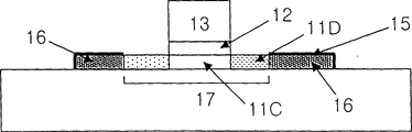
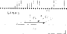
图1A至图1D是描述采用通常方法,使用MIC和MILC方法结晶TFT有源层硅层的截面图。参阅图1A,无定形硅层11形成在绝缘衬底10上,绝缘衬底10上有一缓冲层(未图示),无定形硅层11光刻出图形以便形成有源层。门绝缘层12和门电极13通过使用现有方法形成在有源层11上。如图1B中所示,衬底面用门电极13为掩膜进行掺杂,这样在有源层中形成了源区11S,沟道区11C和漏区11D。如在图1C中所示,光刻胶14被形成以覆盖门电极13和在门电极13之下的源区11S和漏区11D,金属层15沉积在衬底10和光刻胶14之上。如图1D所示,去除光刻胶14之后,整个衬底在300-500℃温度下退火,结果残留物金属层14覆盖的源和漏区16被金属层14引起MIC结晶,金属补偿源和漏区15没有被金属层覆盖,其中门电极13下面的沟道区17分别由金属层14覆盖的源和漏区16的MILC传播而结晶。1A to 1D are cross-sectional views illustrating the crystallization of a silicon layer of a TFT active layer using MIC and MILC methods in a conventional method. Referring to FIG. 1A, an amorphous silicon layer 11 is formed on an
光刻胶14被形成以覆盖邻近门电极13的源和漏区,以防沟道区里的漏电流及其工作特性的退化。如果金属层15被形成以覆盖整个源和漏区,将产生漏电流和工作特性的退化,因为造成MIC的金属成分仍然留在沟道区11C以及沟道区和源和漏区之间的边界中。除了沟道区,源和漏区的运作本质上不受残留金属成分的影响,距离沟道区0.01-5μm的源和漏区被由MIC金属造成的MIC结晶。同时,沟道区与靠近沟道区的源和漏区被由MIC金属造成的和从MIC金属传播的MILC结晶。仅仅沟道区及其下面被MILC结晶,整个有源层所需要的结晶时间可以明显减少。但是,当使用图1A至1D中的过程时,形成光刻胶层的步骤,曝光和去除光刻胶的步骤应该包含在通常TFT制造过程中。A
图2A至图2D是描述通过使用固相结晶(SPC)方法制造结晶硅TFT过程的截面图,这过程包含一形成轻掺杂漏(LDD)区的步骤。如果LDD区形成在漏区中,它可以减少晶体管的关断电流和稳定晶体管的其它电气特征。2A to 2D are cross-sectional views illustrating a process of manufacturing a crystalline silicon TFT by using a solid phase crystallization (SPC) method, which includes a step of forming a lightly doped drain (LDD) region. If the LDD region is formed in the drain region, it can reduce the off current of the transistor and stabilize other electrical characteristics of the transistor.
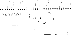
如在图2A中所示,有源层21作出图形,在高温下长时间经受热处理,以便对其进行固相结晶,在这个情况中,衬底是用能经受高温的石英做成的。如在图2B中所示,为了形成一轻掺杂漏(LDD)区,门绝缘层22、下门电极23和上门电极24相继形成在有源层21上。然后,将离子掺杂步骤分两个阶段实现。在离子掺杂第一阶段,如图2C所示,掺入高浓度杂质来形成源区21S和漏区21D。然后如图2D所示,上门电极24被去掉,掺入低浓度杂质来形成轻掺杂漏(LDD)区21LDD。然后,按照通常方法形成一覆盖层和金属连线,制造带LDD区的TFT。通过在TFT有源层中形成LDD区,可以减少TFT的关断电流和稳定其它电气特征。因此,如图1A至1D所示,甚至当用MIC和MILC方法制造TFT的时候,也希望在有源层中形成一LDD区。As shown in FIG. 2A, the active layer 21 is patterned and subjected to heat treatment at a high temperature for a long time to perform solid phase crystallization thereof, and in this case, the substrate is made of high temperature resistant quartz. As shown in FIG. 2B , in order to form a lightly doped drain (LDD) region, a gate insulating layer 22 , a lower gate electrode 23 and an upper gate electrode 24 are sequentially formed on the active layer 21 . Then, the ion doping step is realized in two stages. In the first stage of ion doping, as shown in FIG. 2C , high-concentration impurities are doped to form source region 21S and drain region 21D. Then, as shown in FIG. 2D , the upper gate electrode 24 is removed, and doped with low-concentration impurities to form a lightly doped drain (LDD) region 21LDD. Then, a cover layer and metal wiring are formed according to the usual method to manufacture a TFT with an LDD region. By forming the LDD region in the TFT active layer, it is possible to reduce the off current of the TFT and stabilize other electrical characteristics. Therefore, as shown in FIGS. 1A to 1D, even when TFTs are fabricated by the MIC and MILC methods, it is desirable to form an LDD region in the active layer.
发明内容Contents of the invention
本发明针对制造含结晶硅有源层的薄膜晶体管的方法,因而从根本上解决了上面提到问题和原有技术的不足之处。The present invention is aimed at a method for manufacturing a thin film transistor containing an active layer of crystalline silicon, thus fundamentally solving the above-mentioned problems and the deficiencies of the prior art.
本发明的目的是要提供一个制造含结晶硅有源层的薄膜晶体管方法,按此方法不用如图1所示的形成和去除光刻胶层的步骤,便可在有源层形成一个轻掺杂漏(LDD)区,而且MIC源金属不留在沟道区及其邻近之处。The object of the present invention is to provide a thin-film transistor method for manufacturing an active layer containing crystalline silicon, by which a lightly doped layer can be formed in the active layer without the steps of forming and removing a photoresist layer as shown in Figure 1. The heterogeneous drain (LDD) region, and the MIC source metal does not remain in the channel region and its vicinity.
本发明的另一个目的是要提供一个制造含结晶硅有源层的薄膜晶体管方法,其中包括在有源层形成一个补偿结,在形成轻掺杂漏(LDD)区过程中去掉低浓度掺杂步骤,MIC源金属不留在沟道区和不需要形成和去除光刻胶层的过程。Another object of the present invention is to provide a thin-film transistor method for manufacturing an active layer containing crystalline silicon, which includes forming a compensation junction in the active layer and removing low-concentration doping in the process of forming a lightly doped drain (LDD) region. step, the MIC source metal does not remain in the channel region and does not require the process of forming and removing the photoresist layer.
为了达到本发明上述的和其他的目的,按本发明的方法通过金属诱发结晶制作薄膜晶体管TFT,它包含结晶硅有源层、有源层中的门电极、轻掺杂漏(LDD)区或者补偿结区,其中金属诱发结晶是由有源层的沟道区补偿,它通过使用掩膜形成有源层中的轻掺杂漏(LDD)区或者补偿结区。In order to achieve the above-mentioned and other objects of the present invention, a thin film transistor TFT is made by metal-induced crystallization according to the method of the present invention, which comprises a crystalline silicon active layer, a gate electrode in the active layer, a lightly doped drain (LDD) region or The compensation junction region, where the metal-induced crystallization is compensated by the channel region of the active layer, forms a lightly doped drain (LDD) region or compensation junction region in the active layer by using a mask.
通过下面详尽的描述,本发明的附加特征和优点将被提出或者将变得明显。特别通过书面的描述,权利要求以及附图,将要实现和达到本发明的目标和其它优点。Additional features and advantages of the present invention will be set forth, or will become apparent, from the following detailed description. The objectives and other advantages of the invention will be realized and attained, particularly by the written description, claims as well as the accompanying drawings.
附图说明Description of drawings
本发明实施例的叙述将参考附图,其中:The description of the embodiments of the invention will refer to the accompanying drawings, in which:
图1A至图1D是描述采用现有方法使用MIC和MILC制造结晶硅TFT的截面图;1A to 1D are cross-sectional views describing the fabrication of crystalline silicon TFTs using MICs and MILCs using existing methods;
图2A至图2E是描述采用另一种现有方法制造结晶硅TFT的过程的截面图,这过程包含一形成轻掺杂漏(LDD)区的步骤;2A to 2E are cross-sectional views describing the process of manufacturing a crystalline silicon TFT using another conventional method, which includes a step of forming a lightly doped drain (LDD) region;
图3A至图3F是描述按照本发明第一种优选实施例制造结晶硅TFT的过程的截面图;3A to 3F are cross-sectional views describing the process of manufacturing a crystalline silicon TFT according to a first preferred embodiment of the present invention;
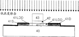
图4A至图4F是描述按照本发明第二种优选实施例制造结晶硅TFT的过程的截面图;4A to 4F are cross-sectional views describing the process of manufacturing a crystalline silicon TFT according to a second preferred embodiment of the present invention;
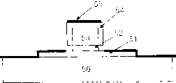
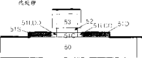
图5A至图5E是描述按照本发明第三种优选实施例制造结晶硅TFT的过程的截面图;5A to 5E are cross-sectional views describing the process of manufacturing a crystalline silicon TFT according to a third preferred embodiment of the present invention;
图6A至图6E是描述按照本发明第四种优选实施例制造结晶硅TFT的过程的截面图;6A to 6E are cross-sectional views describing the process of manufacturing a crystalline silicon TFT according to a fourth preferred embodiment of the present invention;
图7A至图7G是描述按照本发明第五种优选实施例制造结晶硅TFT的过程的截面图;7A to 7G are cross-sectional views describing the process of manufacturing a crystalline silicon TFT according to a fifth preferred embodiment of the present invention;
图8A至图8E是描述按照本发明第六种优选实施例制造结晶硅TFT的过程的截面图。8A to 8E are cross-sectional views illustrating a process of manufacturing a crystalline silicon TFT according to a sixth preferred embodiment of the present invention.
具体实施方式Detailed ways
参阅本发明优选实施例,这些实施例结合附图描述。Reference is now made to the preferred embodiments of the invention, which are described in conjunction with the accompanying drawings.
图3A至图3F是描述按照本发明第一种优选实施例使用MILC制造结晶硅TFT的连续过程的截面图。参阅图3A,形成TFT有源层的无定形硅层31在绝缘衬底30上形成并作出图形,门绝缘层32、下门电极33和上门电极34形成在无定形硅层31上。参阅图3B,通过用门电极34为掩膜,在无定形硅层31上掺入高浓度杂质,以形成源区31S和漏区31D。当制造NMOS(N-沟道金属氧化物半导体)TFT的时候,通过使用离子照射掺杂方法、离子注入方法或者另一种如图3B过程的离子注入方法,对硅层31掺入PH3,P和As杂质,剂量为1E14-1E22/cm3(更可取为1E15-1E21/cm3),能量为10-200KeV(更可取为30-100KeV)。另一方面,当制造PMOS(P沟道金属氧化物半导体)的时候,在图3B的过程中,对硅层31掺入B2H6、B和BH3杂质,剂量为1E13-1E22/cm3(更可取为1E14-1E21/cm3),能量为20-70KeV。3A to 3F are cross-sectional views illustrating a continuous process of manufacturing a crystalline silicon TFT using MILC according to a first preferred embodiment of the present invention. Referring to FIG. 3A , an
然后如在图3C中所示,通过用门电极34作为掩膜,在无定形硅层31和衬底30上形成金属层35,如Ni,及无定形硅层31的结晶。为了诱发无定形硅层结晶,Ni或者Pd是更可取的,但是其它金属例如Ti、Ag、Au、Al、Sn、Sb、Cu、Co、Cr、Mo、Tr、Ru、Rh、Cd和Pt或者其它含有至少这些金属之一的材料也能被用来形成金属层35。Ni,Pd等金属通过溅射、热蒸发、PECVD(等离子体增强化学汽相淀积)、溶液涂覆或者离子注入等方法施加于硅层上,包含此金属的硅层再结晶。但是,用溅射方法形成金属层35是更可取的,金属层35的厚度可以在无定形硅31的诱发结晶适当的范围内被选择。金属层35的厚度大约为1至10000,大约10至200更可取。如果上门电极34的宽度大于下门电极33,诱发结晶的金属层不在标示31LDD硅层的形成LDD区的部分形成,因此,诱发结晶的金属层从沟道区31C按照预定距离补偿。如果沟道区不经沟道区31C和金属层35之间的金属补偿区而直接与诱发结晶的金属层接触,用于减少在硅层结晶的金属成分在硅层结晶后存留于沟道区,于是,残留的金属成分损坏了晶体管的特性。在本发明中,在诱发结晶的金属和沟道区之间的金属补偿区的宽度设定在100-20,000范围内,更可取的金属补偿区的宽度在5,000一20,000范围内,其中沟道区用于以后形成LDD区31LDD。在本发明中,高浓度掺杂的浓度和MIC金属形成过程可以变换而不影响本发明的效能。Then, as shown in FIG. 3C, a
在形成诱发结晶的金属35之后,如图3D所示上门电极34被去掉。然后,如图3E所示,用下门电极33作为掩膜以低浓度掺杂,于是在沟道区31C的下面形成LDD区。在图3E的低浓度掺杂的过程中,硅层31用如PH3、P和As掺杂,其剂量为1E11-1E20/cm3,用离子照射、离子注入方法或者其它离子注入方法制造NMOS(N沟道金属氧化物半导体)TFT。另一方面,当制造PMOS(P沟道金属氧化物半导体)TFT的时候,硅层31用如B2H6、B和BH3掺杂,在图3E低浓度掺杂的过程中其剂量为1E11-1E20/cm3。After forming the crystallization-inducing
在低浓度掺杂形成LDD区之后,热处理以结晶有源层如图3F所示,绝缘层和接触电极分别在有源层上被形成(未图示),以制造TFT。图3F的热处理可以使用任何引起无定形硅金属诱发结晶(MIC)的方法,例如,RTA(快速热退火)或者ELC(准分子激光结晶)方法可以被作为引起MIC的方法。RTA方法用卤钨灯或氙弧光灯在大约500℃-1200℃的温度下,热处理几秒或者几分钟。ELC方法用准分子激光在短的时间内加热有源层到非常高的温度。特别地,在本发明中,退火步骤建议在温度为400℃-600℃的熔炉中退火0.1-50小时,更可取为0.5-20小时。由于熔炉退火方法在低于使玻璃衬底损形的温度下结晶无定形硅,玻璃衬底的损形或者损伤可以被阻止。此外,因为熔炉退火方法可以同时加工多个衬底,它从根本上提高了过程的生产效率。在热处理期间,被MIC金属盖住的硅层部分由MIC源金属引起MIC结晶,没有被MIC金属盖住的硅层部分被MILC结晶,MILC是从MIC地区传播到应用MIC金属的区域。此外,由于经过MIC结晶无定形硅层的热处理条件类似于激活注入在有源层中杂质的退火条件,有源层的结晶和杂质的激活可以在一个步骤中进行。After low concentration doping to form the LDD region, heat treatment to crystallize the active layer. As shown in FIG. 3F, an insulating layer and a contact electrode are respectively formed on the active layer (not shown) to manufacture a TFT. The heat treatment of FIG. 3F can use any method for inducing metal-induced crystallization (MIC) of amorphous silicon, for example, RTA (rapid thermal annealing) or ELC (excimer laser crystallization) method can be used as a method for inducing MIC. The RTA method uses a tungsten-halogen lamp or a xenon arc lamp at a temperature of about 500°C-1200°C for a few seconds or a few minutes. The ELC method uses an excimer laser to heat the active layer to a very high temperature in a short period of time. In particular, in the present invention, the annealing step is recommended to be annealed in a furnace at a temperature of 400°C-600°C for 0.1-50 hours, more preferably 0.5-20 hours. Since the furnace annealing method crystallizes the amorphous silicon at a temperature lower than the temperature at which the glass substrate becomes deformed, the deformed or damaged glass substrate can be prevented. Furthermore, because the furnace annealing method can process multiple substrates simultaneously, it radically improves the productivity of the process. During heat treatment, the part of the silicon layer covered by the MIC metal is crystallized by the MIC source metal, and the part of the silicon layer not covered by the MIC metal is crystallized by the MILC, which propagates from the MIC region to the region where the MIC metal is applied. Furthermore, since the heat treatment conditions for crystallizing the amorphous silicon layer through MIC are similar to the annealing conditions for activating the impurities implanted in the active layer, crystallization of the active layer and activation of the impurities can be performed in one step.
按照前面提到的方法制造TFT的时候,为了从沟道区补偿MIC金属,不必包含形成光刻图形的步骤可以形成金属补偿区,一个带有LDD区的TFT可通过在金属补偿区简单地进行低浓度掺杂而被制造出来,该晶体管有低的漏电流和稳定的电气特征。虽然为了叙述方便,图3A-3F中显示了第一优选实施例,本发明也能举出其它的实施例并将在下面描述,其它实施例的步骤条件与第一实施例一样,除非在描述中另加了说明。When manufacturing a TFT according to the aforementioned method, in order to compensate the MIC metal from the channel region, it is not necessary to include the step of forming a photolithographic pattern to form a metal compensation region. A TFT with an LDD region can be simply formed in the metal compensation region. Manufactured with low concentration doping, the transistor has low leakage current and stable electrical characteristics. Although the first preferred embodiment is shown in Figs. 3A-3F for ease of description, the present invention can also enumerate other embodiments and will be described below, and the step conditions of other embodiments are the same as the first embodiment, unless described Added an explanation in .
图4A至图4F是描述按照本发明第二种优选实施例制造结晶硅TFT过程的截面图。参阅图4A,形成TFT有源层的无定形硅层41在绝缘衬底40上形成并作出图形,门绝缘层42和门电极43形成在无定形硅层41上。如图4A所示,过去常用于形成门电极43的光刻胶44并留在门电极上,门电极43过腐蚀在光刻胶44之下形成倒边。然后,如图4B所示掺高浓度杂质来形成源区41S和漏区41D,如图4C所示用光刻胶44作为掩膜在硅层上形成MIC源金属45。如同第一种实施例提到的那样,高浓度掺杂过程的浓度和MIC金属的形成步骤可以在本发明的范围以内和不影响本发明的效能下被变换。在这个情况中,由于MIC金属不是形成在标示为41LDD的形成LDD区的部分,一金属补偿区形成在门电极43的周围,然后如图4D所示光刻胶44被去除。如图4E所示,用门电极43为掩膜掺低浓度杂质来形成LDD区的41LDD。最后如图4F所示,热处理结晶有源层并按照通常的方法制造晶体管。4A to 4F are cross-sectional views illustrating a process of manufacturing a crystalline silicon TFT according to a second preferred embodiment of the present invention. Referring to FIG. 4A , an
图5A至图5E是描述按照本发明第三种优选实施例制造结晶硅TFT的方法的截面图。参阅图5A,形成TFT有源层的无定形硅层51在绝缘衬底50上形成并作出图形,门绝缘层52和门电极53形成在无定形硅层51上。如图5B所示,用门电极53作为掩膜掺低浓度杂质。对门电极53作阳极氧化处理在门电极53表面上形成阳极氧化物层54。然后如图5C所示,在整个衬底表面上形成MIC源金属55,阳极氧化物层54在门电极53周围建立一金属补偿区。然后,如图5D所示掺高浓度杂质来形成源区51S和漏区51D。如上所述,高浓度掺杂过程的浓度和MIC金属的形成步骤可以在本发明的范围以内和不影响本发明的效能下被变换。然后如图5E所示,热处理结晶有源层并按照通常的方法制造晶体管。按照本发明,在门电极53上阳极氧化层54覆盖的部分不进行高浓度杂质掺杂,因此在门电极53下形成一个LDD区。5A to 5E are cross-sectional views illustrating a method of manufacturing a crystalline silicon TFT according to a third preferred embodiment of the present invention. Referring to FIG. 5A , an
图6A至图6E是描述按照本发明第四种优选实施例制造结晶硅TFT的方法的截面图。参阅图6A,形成TFT有源层的无定形硅层61在绝缘衬底60上形成并作出图形,门绝缘层62和门电极63形成在无定形硅层61上。图6A显示一状态,其中将以前用于形成门电极63的光刻胶64留在门电极上,光刻胶64在一比光刻胶硬烘温度更高的温度下重新流动。然后,如图6B所示利用重新流动的光刻胶作为掩膜来掺高浓度杂质在有源区中形成源区和漏区。然后如图6C所示,在整个衬底表面上形成MIC源金属55,如图6D所示,重新流动的光刻胶64被去除,掺低浓度杂质在有源层中形成标示为61LDD的LDD区。因为MIC源金属不是形成在LDD区61LDD上,当形成LDD区的时候,一金属补偿区同时在门电极周围被形成.如上所述,高浓度掺杂过程的浓度和MIC金属的形成步骤可以在本发明的范围以内和不影响本发明的效能下被变换。如图6E所示,热处理结晶有源层并按照先前的技术制造晶体管。6A to 6E are cross-sectional views illustrating a method of manufacturing a crystalline silicon TFT according to a fourth preferred embodiment of the present invention. Referring to FIG. 6A , an
图7A至图7E是描述按照本发明第五种优选实施例制造结晶硅TFT的方法的截面图。参阅图7A,形成TFT有源层的无定形硅层71在绝缘衬底70上形成并作出图形,门绝缘层72和门电极73形成在无定形硅层71上。然后,如图7B所示,绝缘层74被形成。当在图7B的结构上进行各向异性蚀刻时,如图7C所示,在门绝缘层72和门电极73的侧表面上留下一侧墙75,利用侧墙75,也能取得上述实施例的效果。也就是说,如果如图7D所示在低能进行高浓度掺杂和如图7E所示在高能进行低浓度掺杂,可以在侧墙75下面的有源层上形成LDD区。然后,如图7F所示形成MIC源金属76,如图7G所示进行热处理结晶有源层。此后,按照通常方法制造晶体管,如上所述,MIC金属也能在掺杂步骤以前形成。7A to 7E are cross-sectional views illustrating a method of manufacturing a crystalline silicon TFT according to a fifth preferred embodiment of the present invention. Referring to FIG. 7A , an
图8A至图8E是描述按照本发明第六种优选实施例制造TFT的方法的截面图。参阅图8A,形成TFT有源层的无定形硅层81在绝缘衬底80上形成并作出图形,门绝缘层82和门电极83形成在无定形硅层81上。在这个实施例中,当蚀刻门电极83和门绝缘层82的时候,仅门电极83过蚀刻以建立倒边部分。结果如图8A所示,形成的门绝缘层82比门电极83更宽。使用门绝缘层82和门电极83,也能取得上述实施例的效果。也就是说,如果分别进行低能高浓度掺杂(图8B)和高能低浓度掺杂(图8C),在门绝缘层82覆盖的有源层中仅形成低浓度掺杂。于是,仅在门绝缘层82覆盖而门电极83没有覆盖的有源层中形成LDD区,然后如图8D所示形成MIC金属84,如Ni。如图8E所示进行热处理结晶有源层。此后,按照通常方法制造晶体管,如上所述,MIC金属也能在掺杂步骤以前形成。8A to 8E are cross-sectional views describing a method of manufacturing a TFT according to a sixth preferred embodiment of the present invention. Referring to FIG. 8A , an
在上述所有的实施例中,低浓度掺杂的步骤可以被省略。于是本发明的实施例可用于制造带LDD区但不带补偿结区的TFT。In all the above-mentioned embodiments, the step of low concentration doping can be omitted. Embodiments of the present invention can then be used to fabricate TFTs with LDD regions but without compensating junction regions.
如同前面描述的那样,按照本发明制造TFT方法使用一个附加光刻胶形成步骤形成一金属补偿区,以低浓度对金属补偿区掺杂以形成LDD区。结果,按本发明制造的晶体管在关态有低漏电流和在开态有稳定的电气特性。As described above, the TFT manufacturing method according to the present invention uses an additional photoresist forming step to form a metal compensation region, and dope the metal compensation region at a low concentration to form an LDD region. As a result, transistors manufactured according to the present invention have low leakage current in the off state and stable electrical characteristics in the on state.
虽然为了描述已给出了本发明的实施例,但在不背离本发明的范围和精神下各种技术的修改、增加和代用是可能的,本发明对此表示欣赏,本发明的范围和精神将在所附的权利要求书及其等同中给定。Although the embodiment of the present invention has been given for the purpose of description, the present invention appreciates that various technical modifications, additions and substitutions are possible without departing from the scope and spirit of the present invention. as set forth in the appended claims and their equivalents.
Claims (11)
Applications Claiming Priority (2)
| Application Number | Priority Date | Filing Date | Title |
|---|---|---|---|
| KR0072592/2000 | 2000-12-01 | ||
| KR10-2000-0072592A KR100390522B1 (en) | 2000-12-01 | 2000-12-01 | Method for fabricating thin film transistor including a crystalline silicone active layer |
Publications (2)
| Publication Number | Publication Date |
|---|---|
| CN1355554A CN1355554A (en) | 2002-06-26 |
| CN1187802C true CN1187802C (en) | 2005-02-02 |
Family
ID=19702576
Family Applications (1)
| Application Number | Title | Priority Date | Filing Date |
|---|---|---|---|
| CNB011415770A Expired - Fee Related CN1187802C (en) | 2000-12-01 | 2001-10-22 | Method for manufacturing thin film transistor containing crystallization silicon active layer |
Country Status (5)
| Country | Link |
|---|---|
| US (1) | US6548331B2 (en) |
| JP (1) | JP3713232B2 (en) |
| KR (1) | KR100390522B1 (en) |
| CN (1) | CN1187802C (en) |
| TW (1) | TW517289B (en) |
Families Citing this family (82)
| Publication number | Priority date | Publication date | Assignee | Title |
|---|---|---|---|---|
| US20040029310A1 (en) * | 2000-08-18 | 2004-02-12 | Adoft Bernds | Organic field-effect transistor (ofet), a production method therefor, an integrated circut constructed from the same and their uses |
| WO2002015264A2 (en) * | 2000-08-18 | 2002-02-21 | Siemens Aktiengesellschaft | Encapsulated organic-electronic component, method for producing the same and use thereof |
| DE10044842A1 (en) * | 2000-09-11 | 2002-04-04 | Siemens Ag | Organic rectifier, circuit, RFID tag and use of an organic rectifier |
| EP1323195A1 (en) * | 2000-09-22 | 2003-07-02 | Siemens Aktiengesellschaft | Electrode and/or conductor track for organic components and production method therefor |
| DE10061297C2 (en) | 2000-12-08 | 2003-05-28 | Siemens Ag | Procedure for structuring an OFET |
| DE10061286C1 (en) * | 2000-12-08 | 2002-04-04 | Hollingsworth Gmbh | Equipment winding saw-toothed wire under tension onto a carding machine roller, includes a braking unit applying a controlled force against a braking roller |
| DE10061299A1 (en) * | 2000-12-08 | 2002-06-27 | Siemens Ag | Device for determining and / or forwarding at least one environmental influence, production method and use thereof |
| DE10105914C1 (en) * | 2001-02-09 | 2002-10-10 | Siemens Ag | Organic field effect transistor with photo-structured gate dielectric and a method for its production |
| KR100590265B1 (en) * | 2001-03-12 | 2006-06-15 | 삼성에스디아이 주식회사 | Manufacturing Method of Thin Film Transistor Using Metal-Induced Lateral Crystallization |
| EP1374138A2 (en) * | 2001-03-26 | 2004-01-02 | Siemens Aktiengesellschaft | Device with at least two organic electronic components and method for producing the same |
| JP4831885B2 (en) | 2001-04-27 | 2011-12-07 | 株式会社半導体エネルギー研究所 | Method for manufacturing semiconductor device |
| DE10126860C2 (en) * | 2001-06-01 | 2003-05-28 | Siemens Ag | Organic field effect transistor, process for its manufacture and use for the construction of integrated circuits |
| DE10126859A1 (en) * | 2001-06-01 | 2002-12-12 | Siemens Ag | Production of conducting structures used in organic FETs, illuminated diodes, organic diodes and integrated circuits comprises directly or indirectly forming conducting pathways |
| DE10151036A1 (en) | 2001-10-16 | 2003-05-08 | Siemens Ag | Isolator for an organic electronic component |
| DE10151440C1 (en) * | 2001-10-18 | 2003-02-06 | Siemens Ag | Organic electronic component for implementing an encapsulated partially organic electronic component has components like a flexible foil as an antenna, a diode or capacitor and an organic transistor. |
| KR100566894B1 (en) * | 2001-11-02 | 2006-04-04 | 네오폴리((주)) | Crystalline Silicon TFT Panel and Fabrication Method Using MIC |
| JP3978019B2 (en) * | 2001-11-19 | 2007-09-19 | 矢崎化工株式会社 | Separation and recovery method for steel pipe and coating resin in resin-coated steel pipe, and separation and recovery equipment |
| DE10160732A1 (en) * | 2001-12-11 | 2003-06-26 | Siemens Ag | OFET used e.g. in RFID tag, comprises an intermediate layer on an active semiconductor layer |
| DE10212640B4 (en) * | 2002-03-21 | 2004-02-05 | Siemens Ag | Logical components made of organic field effect transistors |
| DE10212639A1 (en) * | 2002-03-21 | 2003-10-16 | Siemens Ag | Device and method for laser structuring functional polymers and uses |
| DE10226370B4 (en) * | 2002-06-13 | 2008-12-11 | Polyic Gmbh & Co. Kg | Substrate for an electronic component, use of the substrate, methods for increasing the charge carrier mobility and organic field effect transistor (OFET) |
| WO2004017439A2 (en) | 2002-07-29 | 2004-02-26 | Siemens Aktiengesellschaft | Electronic component comprising predominantly organic functional materials and method for the production thereof |
| DE50309888D1 (en) * | 2002-08-08 | 2008-07-03 | Polyic Gmbh & Co Kg | ELECTRONIC DEVICE |
| DE50306683D1 (en) | 2002-08-23 | 2007-04-12 | Polyic Gmbh & Co Kg | ORGANIC COMPONENT FOR OVERVOLTAGE PROTECTION AND ASSOCIATED CIRCUIT |
| JP2006505927A (en) * | 2002-11-05 | 2006-02-16 | ポリアイシー ゲーエムベーハー ウント コー、 カーゲー | Organic electronic element having high resolution structure and method of manufacturing the same |
| KR100466628B1 (en) | 2002-11-12 | 2005-01-15 | 삼성에스디아이 주식회사 | Flat panel display and fabrication method thereof |
| DE10253154A1 (en) | 2002-11-14 | 2004-05-27 | Siemens Ag | Biosensor, used to identify analyte in liquid sample, has test field with detector, where detector registers field changes as electrical signals for evaluation |
| ATE540436T1 (en) * | 2002-11-19 | 2012-01-15 | Polyic Gmbh & Co Kg | ORGANIC ELECTRONIC COMPONENT WITH THE SAME ORGANIC MATERIAL FOR AT LEAST TWO FUNCTIONAL LAYERS |
| ES2282708T3 (en) * | 2002-11-19 | 2007-10-16 | POLYIC GMBH & CO. KG | ORGANIC ELECTRONIC COMPONENT WITH STRUCTURED SEMI-CONDUCTING FUNCTIONAL COAT AND METHOD TO PRODUCE THE SAME. |
| TW559896B (en) * | 2002-12-17 | 2003-11-01 | Ind Tech Res Inst | Method of forming TFT and forming TFT on color filter |
| DE10300521A1 (en) * | 2003-01-09 | 2004-07-22 | Siemens Ag | Organoresistive memory |
| EP1586127B1 (en) * | 2003-01-21 | 2007-05-02 | PolyIC GmbH & Co. KG | Organic electronic component and method for producing organic electronic devices |
| DE10302149A1 (en) * | 2003-01-21 | 2005-08-25 | Siemens Ag | Use of conductive carbon black / graphite blends for the production of low-cost electronics |
| US9369775B2 (en) | 2003-01-31 | 2016-06-14 | At&T Intellectual Property I, L.P. | Methods and systems for delivering signals from cable networks to telecommunications networks |
| CN1774806B (en) | 2003-02-14 | 2010-06-16 | 日本电气株式会社 | Line element and semiconductor circuit using the same |
| KR100956339B1 (en) | 2003-02-25 | 2010-05-06 | 삼성전자주식회사 | Silicon Crystallization System and Silicon Crystallization Method |
| KR100530041B1 (en) * | 2003-03-28 | 2005-11-22 | 주승기 | Method for Forming Poly-Si Film Using Ni Alloy Film and Method for Forming Thin Film Transistor Using the Same |
| TWI226660B (en) * | 2003-04-01 | 2005-01-11 | Univ Nat Taiwan | Method of fabricating polysilicon film by Nickel/Copper induced lateral crystallization |
| CN100358156C (en) * | 2003-05-06 | 2007-12-26 | Pt普拉斯有限公司 | Storing capacitor structure for LCD board and OELD board |
| KR100928490B1 (en) * | 2003-06-28 | 2009-11-26 | 엘지디스플레이 주식회사 | LCD panel and manufacturing method thereof |
| DE10330064B3 (en) * | 2003-07-03 | 2004-12-09 | Siemens Ag | Organic logic gate has load field effect transistor with potential-free gate electrode in series with switching field effect transistor |
| DE10330062A1 (en) * | 2003-07-03 | 2005-01-27 | Siemens Ag | Method and device for structuring organic layers |
| US7354808B2 (en) * | 2003-08-15 | 2008-04-08 | Semiconductor Energy Laboratory Co., Ltd. | Resist composition and method for manufacturing semiconductor device using the same |
| DE10338277A1 (en) * | 2003-08-20 | 2005-03-17 | Siemens Ag | Organic capacitor with voltage controlled capacity |
| DE10339036A1 (en) | 2003-08-25 | 2005-03-31 | Siemens Ag | Organic electronic component with high-resolution structuring and manufacturing method |
| DE10340643B4 (en) * | 2003-09-03 | 2009-04-16 | Polyic Gmbh & Co. Kg | Printing method for producing a double layer for polymer electronics circuits, and thereby produced electronic component with double layer |
| DE10340644B4 (en) * | 2003-09-03 | 2010-10-07 | Polyic Gmbh & Co. Kg | Mechanical controls for organic polymer electronics |
| KR100611224B1 (en) | 2003-11-22 | 2006-08-09 | 삼성에스디아이 주식회사 | Thin film transistor using metal induced lateral crystallization and its manufacturing method |
| KR100588779B1 (en) * | 2003-12-30 | 2006-06-12 | 동부일렉트로닉스 주식회사 | Semiconductor device and manufacturing method |
| DE102004002024A1 (en) * | 2004-01-14 | 2005-08-11 | Siemens Ag | Self-aligning gate organic transistor and method of making the same |
| US20050236616A1 (en) * | 2004-04-26 | 2005-10-27 | Horng-Huei Tseng | Reliable semiconductor structure and method for fabricating |
| KR100712112B1 (en) * | 2004-06-30 | 2007-04-27 | 삼성에스디아이 주식회사 | Semiconductor device and manufacturing method thereof |
| DE102004040831A1 (en) * | 2004-08-23 | 2006-03-09 | Polyic Gmbh & Co. Kg | Radio-tag compatible outer packaging |
| DE102004059464A1 (en) * | 2004-12-10 | 2006-06-29 | Polyic Gmbh & Co. Kg | Electronic component with modulator |
| DE102004059467A1 (en) * | 2004-12-10 | 2006-07-20 | Polyic Gmbh & Co. Kg | Gate made of organic field effect transistors |
| DE102004059465A1 (en) * | 2004-12-10 | 2006-06-14 | Polyic Gmbh & Co. Kg | recognition system |
| DE102004063435A1 (en) | 2004-12-23 | 2006-07-27 | Polyic Gmbh & Co. Kg | Organic rectifier |
| US7309895B2 (en) | 2005-01-25 | 2007-12-18 | Hewlett-Packard Development Company, L.P. | Semiconductor device |
| DE102005009820A1 (en) * | 2005-03-01 | 2006-09-07 | Polyic Gmbh & Co. Kg | Electronic assembly with organic logic switching elements |
| DE102005009819A1 (en) | 2005-03-01 | 2006-09-07 | Polyic Gmbh & Co. Kg | electronics assembly |
| DE102005017655B4 (en) * | 2005-04-15 | 2008-12-11 | Polyic Gmbh & Co. Kg | Multilayer composite body with electronic function |
| DE102005031448A1 (en) | 2005-07-04 | 2007-01-11 | Polyic Gmbh & Co. Kg | Activatable optical layer |
| DE102005035589A1 (en) | 2005-07-29 | 2007-02-01 | Polyic Gmbh & Co. Kg | Manufacturing electronic component on surface of substrate where component has two overlapping function layers |
| DE102005035590A1 (en) * | 2005-07-29 | 2007-02-01 | Polyic Gmbh & Co. Kg | Electronic component has flexible substrate and stack of layers including function layer on substratesurface |
| DE102005042166A1 (en) * | 2005-09-06 | 2007-03-15 | Polyic Gmbh & Co.Kg | Organic device and such a comprehensive electrical circuit |
| DE102005044306A1 (en) * | 2005-09-16 | 2007-03-22 | Polyic Gmbh & Co. Kg | Electronic circuit and method for producing such |
| ZA200807571B (en) * | 2006-03-01 | 2009-08-26 | Ethypharm Sa | Crush-resistant tablets intended to prevent accidental misuse and unlawful diversion |
| KR100770266B1 (en) * | 2006-11-10 | 2007-10-25 | 삼성에스디아이 주식회사 | Organic light emitting display device and manufacturing method |
| KR101084261B1 (en) | 2010-03-17 | 2011-11-16 | 삼성모바일디스플레이주식회사 | Thin film transistor, display device having same, and manufacturing method thereof |
| CN102751200B (en) * | 2012-06-29 | 2015-06-10 | 京东方科技集团股份有限公司 | Thin film transistor, array substrateand manufacturing method thereof |
| KR102086626B1 (en) * | 2012-11-23 | 2020-03-11 | 한국전자통신연구원 | Self-aligned thin film transistor and fabrication method thereof |
| CN103413783B (en) * | 2013-07-31 | 2016-02-24 | 北京京东方光电科技有限公司 | Array base palte and preparation method thereof, display unit |
| KR102235421B1 (en) * | 2013-12-06 | 2021-04-01 | 엘지디스플레이 주식회사 | Array substrate and method of fabricating the same |
| CN103794566A (en) | 2014-01-17 | 2014-05-14 | 深圳市华星光电技术有限公司 | Method for manufacturing display panel |
| CN104681628A (en) * | 2015-03-17 | 2015-06-03 | 京东方科技集团股份有限公司 | Polycrystalline silicon thin film transistor, array substrate, manufacturing methods and display device |
| JP6434872B2 (en) * | 2015-07-31 | 2018-12-05 | 東芝メモリ株式会社 | Semiconductor device |
| JP6851166B2 (en) * | 2015-10-12 | 2021-03-31 | 株式会社半導体エネルギー研究所 | Manufacturing method of semiconductor device |
| CN106129086B (en) * | 2016-07-21 | 2019-04-30 | 深圳市华星光电技术有限公司 | TFT substrate and preparation method thereof |
| CN118763123A (en) * | 2019-09-24 | 2024-10-11 | 乐金显示有限公司 | Thin film transistor, substrate thereof, and display device including the thin film transistor |
| US12439677B2 (en) | 2021-08-16 | 2025-10-07 | Changxin Memory Technologies, Inc. | Method for manufacturing semiconductor device, and semiconductor device |
| CN115938923A (en) * | 2021-08-16 | 2023-04-07 | 长鑫存储技术有限公司 | A kind of preparation method of semiconductor device and semiconductor device |
| KR102921360B1 (en) * | 2021-10-27 | 2026-02-02 | 삼성디스플레이 주식회사 | transistor array substrate and manufacturing method thereof |
Family Cites Families (19)
| Publication number | Priority date | Publication date | Assignee | Title |
|---|---|---|---|---|
| JP2948965B2 (en) * | 1991-12-02 | 1999-09-13 | 松下電器産業株式会社 | Method for manufacturing thin film transistor |
| JPH05175230A (en) * | 1991-12-20 | 1993-07-13 | Toshiba Corp | Method of manufacturing thin film transistor |
| TW226478B (en) * | 1992-12-04 | 1994-07-11 | Semiconductor Energy Res Co Ltd | Semiconductor device and method for manufacturing the same |
| TW241377B (en) | 1993-03-12 | 1995-02-21 | Semiconductor Energy Res Co Ltd | |
| JP3190482B2 (en) * | 1993-05-21 | 2001-07-23 | 株式会社半導体エネルギー研究所 | Semiconductor device and manufacturing method thereof |
| US5488000A (en) | 1993-06-22 | 1996-01-30 | Semiconductor Energy Laboratory Co., Ltd. | Method of fabricating a thin film transistor using a nickel silicide layer to promote crystallization of the amorphous silicon layer |
| US5581092A (en) * | 1993-09-07 | 1996-12-03 | Semiconductor Energy Laboratory Co., Ltd. | Gate insulated semiconductor device |
| JP2759415B2 (en) * | 1993-11-05 | 1998-05-28 | 株式会社半導体エネルギー研究所 | Method for manufacturing semiconductor device |
| TW272319B (en) | 1993-12-20 | 1996-03-11 | Sharp Kk | |
| JPH07321329A (en) * | 1994-05-27 | 1995-12-08 | Matsushita Electric Ind Co Ltd | Method of manufacturing thin film transistor and liquid crystal display device |
| US6300659B1 (en) * | 1994-09-30 | 2001-10-09 | Semiconductor Energy Laboratory Co., Ltd. | Thin-film transistor and fabrication method for same |
| JP3476320B2 (en) * | 1996-02-23 | 2003-12-10 | 株式会社半導体エネルギー研究所 | Semiconductor thin film and method for manufacturing the same, semiconductor device and method for manufacturing the same |
| JPH10150201A (en) * | 1996-11-19 | 1998-06-02 | Matsushita Electric Ind Co Ltd | Method for manufacturing thin film transistor |
| JPH10173200A (en) * | 1996-12-12 | 1998-06-26 | Semiconductor Energy Lab Co Ltd | Manufacture or semiconductor device |
| JPH118394A (en) * | 1997-06-18 | 1999-01-12 | Semiconductor Energy Lab Co Ltd | Semiconductor device and manufacture of the same |
| US6066547A (en) | 1997-06-20 | 2000-05-23 | Sharp Laboratories Of America, Inc. | Thin-film transistor polycrystalline film formation by nickel induced, rapid thermal annealing method |
| KR100276378B1 (en) | 1997-11-12 | 2001-01-15 | 주승기 | Thin film transistor and its manufacturing method |
| KR100340124B1 (en) | 1998-02-10 | 2003-01-29 | 주승기 | Method of manufacturing thin film transistor |
| US6278130B1 (en) * | 1998-05-08 | 2001-08-21 | Seung-Ki Joo | Liquid crystal display and fabricating method thereof |
-
2000
- 2000-12-01 KR KR10-2000-0072592A patent/KR100390522B1/en not_active Expired - Fee Related
-
2001
- 2001-04-04 US US09/826,439 patent/US6548331B2/en not_active Expired - Fee Related
- 2001-10-22 CN CNB011415770A patent/CN1187802C/en not_active Expired - Fee Related
- 2001-11-02 TW TW090127265A patent/TW517289B/en not_active IP Right Cessation
- 2001-11-30 JP JP2001366065A patent/JP3713232B2/en not_active Expired - Fee Related
Also Published As
| Publication number | Publication date |
|---|---|
| KR100390522B1 (en) | 2003-07-07 |
| TW517289B (en) | 2003-01-11 |
| JP3713232B2 (en) | 2005-11-09 |
| KR20020043116A (en) | 2002-06-08 |
| US6548331B2 (en) | 2003-04-15 |
| US20020068392A1 (en) | 2002-06-06 |
| JP2002208599A (en) | 2002-07-26 |
| CN1355554A (en) | 2002-06-26 |
Similar Documents
| Publication | Publication Date | Title |
|---|---|---|
| CN1187802C (en) | Method for manufacturing thin film transistor containing crystallization silicon active layer | |
| CN1167114C (en) | Method for manufacturing thin film transistor with polycrystalline active layer | |
| KR100355938B1 (en) | Semiconductor device manufacturing method | |
| CN1113409C (en) | Method of manufacturing semiconductor device having diffrent orientations of crystal channel growth | |
| US8253141B2 (en) | Thin film transistor, method of fabricating the same, and organic light emitting diode display device including the thin film transistor | |
| US6586287B2 (en) | Method for fabricating thin film transistor including crystalline silicon active layer | |
| US7303981B2 (en) | Polysilicon structure, thin film transistor panel using the same, and manufacturing method of the same | |
| US7390705B2 (en) | Method for crystallizing amorphous semiconductor thin film by epitaxial growth using non-metal seed and method for fabricating poly-crystalline thin film transistor using the same | |
| TWI322446B (en) | Mask for polycrystallization and method of manufacturing thin film transistor using polycrystallization mask | |
| US7521303B2 (en) | Method of crystallizing amorphous semiconductor thin film and method of fabricating poly crystalline thin film transistor using the same | |
| US20020137310A1 (en) | Method and apparatus for fabricating a semiconductor device | |
| US7309625B2 (en) | Method for fabricating metal oxide semiconductor with lightly doped drain | |
| JP4082459B2 (en) | Manufacturing method of display device | |
| CN1670930A (en) | Fabrication method of metal oxide semiconductor with lightly doped drain | |
| CN101005016A (en) | Polysilicon layer and method for manufacturing thin film transistor | |
| JP4304374B2 (en) | Top gate type thin film transistor | |
| KR100753635B1 (en) | Fabrication Method of Thin Film Transistor with Ldd Structure Using Metal-Induced Lateral Crystallization | |
| KR20050078392A (en) | Crystallization method of amorphous semiconductor thin film, method of manufacturing thin film transistor using the same, and thin film semiconductor device | |
| KR100719919B1 (en) | Polysilicon Thin Film Transistor Formation Method | |
| KR100934328B1 (en) | Polycrystalline silicon thin film transistor having a lower gate and manufacturing method thereof | |
| CN1632932A (en) | A method of manufacturing a thin film transistor | |
| TWI223455B (en) | Crystalline silicon TFT panel having multi-gate structure used for LCD or OELD | |
| JPH10144925A (en) | Method for manufacturing thin-film transistor | |
| KR20050066645A (en) | Fabrication method of liquid crystal display device using metal induced crystallization |
Legal Events
| Date | Code | Title | Description |
|---|---|---|---|
| C10 | Entry into substantive examination | ||
| SE01 | Entry into force of request for substantive examination | ||
| C06 | Publication | ||
| PB01 | Publication | ||
| C14 | Grant of patent or utility model | ||
| GR01 | Patent grant | ||
| C17 | Cessation of patent right | ||
| CF01 | Termination of patent right due to non-payment of annual fee |
Granted publication date: 20050202 Termination date: 20131022 |