EP0001209A1 - Circuit semi-conducteur intégré - Google Patents
Circuit semi-conducteur intégré Download PDFInfo
- Publication number
- EP0001209A1 EP0001209A1 EP78100654A EP78100654A EP0001209A1 EP 0001209 A1 EP0001209 A1 EP 0001209A1 EP 78100654 A EP78100654 A EP 78100654A EP 78100654 A EP78100654 A EP 78100654A EP 0001209 A1 EP0001209 A1 EP 0001209A1
- Authority
- EP
- European Patent Office
- Prior art keywords
- conductors
- cells
- group
- wiring
- active
- Prior art date
- Legal status (The legal status is an assumption and is not a legal conclusion. Google has not performed a legal analysis and makes no representation as to the accuracy of the status listed.)
- Withdrawn
Links
Images


Classifications
-
- H—ELECTRICITY
- H10—SEMICONDUCTOR DEVICES; ELECTRIC SOLID-STATE DEVICES NOT OTHERWISE PROVIDED FOR
- H10D—INORGANIC ELECTRIC SEMICONDUCTOR DEVICES
- H10D84/00—Integrated devices formed in or on semiconductor substrates that comprise only semiconducting layers, e.g. on Si wafers or on GaAs-on-Si wafers
- H10D84/90—Masterslice integrated circuits
- H10D84/901—Masterslice integrated circuits comprising bipolar technology
-
- H—ELECTRICITY
- H10—SEMICONDUCTOR DEVICES; ELECTRIC SOLID-STATE DEVICES NOT OTHERWISE PROVIDED FOR
- H10W—GENERIC PACKAGES, INTERCONNECTIONS, CONNECTORS OR OTHER CONSTRUCTIONAL DETAILS OF DEVICES COVERED BY CLASS H10
- H10W20/00—Interconnections in chips, wafers or substrates
- H10W20/40—Interconnections external to wafers or substrates, e.g. back-end-of-line [BEOL] metallisations or vias connecting to gate electrodes
- H10W20/41—Interconnections external to wafers or substrates, e.g. back-end-of-line [BEOL] metallisations or vias connecting to gate electrodes characterised by their conductive parts
- H10W20/43—Layouts of interconnections
Definitions
- the invention relates to integrated semiconductor circuits and in particular to the arrangement of the integrated circuits on a semiconductor wafer.
- the individual cells are designed to perform a very special function, usually also in a special system.
- the wiring makes this less difficult since it can be fully taken into account when arranging the circuits within the semiconductor die.
- Integrated semiconductor wafers produced in a single design often only exist once and are then manufactured in large quantities. Changing the logical function is extremely difficult and is rarely done.
- the wiring on the surface of a semiconductor wafer consists of connections between the components, supply lines and signal lines.
- the inside of the die for connection between different Functional circuits, called macros, and wiring used between the individual dies are commonly referred to as global wiring.
- the area of a semiconductor chip that is occupied by this global wiring depends on the type of semiconductor chip, i.e. logic circuit or memory, the rules to be observed during the production process and the number of metallization levels available for performing the wiring on the surface of the semiconductor chip from.
- each of the cells contains an active area and space for multiple wiring channels, where the wiring within the cell, within the circuitry, and all of the global wiring can then be housed.
- the cells are housed in closely adjacent column arrangements in order to accommodate as many such cells as possible on a semiconductor wafer can. However, this arrangement is far too rigid.
- the density of well-developed wiring patterns varies with the location on the die. In general, considerably more lines are required in the middle of the plate than, for example, at the edge. If this number of lines exceeds the wiring channels available within a cell, the cell cannot be used. This resulted in the already mentioned poor efficiency when using cells and wiring space.
- US Pat. No. 4,032,962 which corresponds to the applicant's German patent application P 26 55 575, shows an arrangement of how the wiring can be used with higher efficiency.
- This patent discloses semiconductor circuits arranged in columns within the substrate, each circuit having an elongated, doped zone and a group of other doped zones which connect to the former to form diode junctions.
- the elongated zone can accommodate a predetermined largest number of other zones.
- a second device is provided on the narrow side of the first device.
- a first group of lines of a first line level extends over the elongated zone and perpendicular to the longitudinal extent of this zone, these lines being connected to selected ones of the other doped zones.
- Another conductor in a second metallization level on the substrate is connected to a doped zone of the second device and extends essentially parallel to the longitudinal direction of the first zone. In this way, numerous lines, whether used by a particular circuit or not, can be routed across the active area within the substrate used by the semiconductor cells. This type of arrangement has effectively increased the circuit density within the die. However, this arrangement is not aimed at optimal utilization of the surface of the semiconductor provided for the wiring alone.
- the object on which the invention is based can be derived in general terms, namely to further improve the utilization of the surface of a semiconductor die and in particular to further reduce the area to be kept free on the semiconductor surface for global wiring.
- This object on which the invention is based is first achieved in that the area to be kept free for the global wiring channels is separated from the area to be kept free for the active circuits and their wiring on the semiconductor wafer. Each of these two areas is then divided into smaller areas, which are to be referred to as active cells and as wiring cells. As the name suggests, the active cells are used to house the active circuits, and the wiring cells are primarily used for global wiring channels. The dimensions of these cells are designed for predetermined relationships to one another, in a predetermined manner, before the actual production of the actual wiring on the semiconductor die.
- the layout consists of a number of spaced-apart circuits or cells and first and second substantially parallel elongated conductors which lie on a first insulating layer.
- the first group of conductors lies immediately above the active circuits, and the second group of conductors lies in the areas between the circuits which are left free for wiring. Selected connections of the first group of conductors are connected to selected zones of the active components or circuits via bores provided in the first insulating layer.
- a third group of conductors extends perpendicular to the first and second groups of conductors and is disposed over a second insulating layer.
- FIG. 1 shows a known DTL circuit operating as a NAND gate. This circuit is not part of the invention and is well known to those skilled in the semiconductor art. It should also be added immediately that the invention is not limited to this type of circuit, or to a corresponding arrangement in a semiconductor die. In fact, the invention is also applicable to other circuit families, such as. B. TTL, standard DTL, ECL etc. applicable.
- the circuit itself and its various configurations are described in an article by Peltier in the 1975 IEEE International Solid-States Circuits Conference, Digest of Technical Papers, pages 168-169 with the title "A New Approach to Bipolar LSI: CL".
- the circuit consists of a single transistor T1, a pair of bias resistors RB and RC connected to the base and collector electrodes of transistor T1.
- the circuit has six connectable outputs, which are preferably designed as Schottky junction diodes and are accordingly labeled D1, D2, D3, D4, D 5, and D6 are designated, as well as a direct collector connection designated C.
- the logic circuit works by controlling the current flowing through the resistor RB, which can also be a transistor. If all the input signals of the transistor T1 are at low potential, then T1 is blocked and the output signals of the Schottky junction diodes are at high potential. If one of the input signals from T1 is high, T1 conducts from + V to ground and the output Schottky junction diodes are conductive.
- FIGS. 2 and 2A are a top view and a cross-sectional view, respectively, of four cells labeled A11, A12, A21 and A22.
- the cells are practically constructed in the same way, so that the description of a cell stands for the description of all cells.
- Each cell is a DTL circuit in accordance with FIG. 1 in integrated semiconductor circuit technology, and consists of a number of zones of different conductivity types which extend into the semiconductor die and thereby form transistors, diodes and resistors. These zones are applied on a first, above a first insulating layer 31 on the semiconductor die th metallization level to form a basic DTL circuit. Part of the surface wiring has been omitted for clarity. For example, the connecting lines between the resistors RB and RC and the base or collector electrode are not shown in FIG. 2 and are also not shown in the other figures of the drawing. A cross attached in the drawing indicates the areas in which the wiring of the second metallization level above a second insulation layer 34 can cross the wiring of the first metallization level. But this is explained in more detail below. It should first be pointed out that the arrangement of the cells in FIGS. 2, 2A and 3 do not represent the invention. However, they show the currently best known way of realizing the invention.
- Transistor T1 contains an elongated sub-collector zone 10 mounted in the substrate 8, a base zone 11 and an emitter zone 12 formed in an epitaxial layer 26.
- Schottky junction diodes D1, D2 ..., D6 are formed in the epitaxial layer 26 symmetrically on both sides.
- a collector connection zone 14 completes the transistor T1. Isolation between the circuits is formed by a P + conductive zone 16 and an embedded oxide zone 15, as is known in the art.
- the isolation zone 18 isolates the zone 14 from the base 11 and emitter 12. As can be seen from FIG. 2A, only those diodes which are actually switched on in the circuit have a metallization which is necessary for the formation of the diodes.
- connection lines which are designated with + V and ground, provide the reference potentials for each circuit and are mounted above the insulating layer 31 perpendicular to the longitudinal direction of the cell.
- the resistors RB and RC are elongated on both long sides of each cell.
- the lines connecting the cells to one another are produced in a first and a second metallization level and form functional units, which are referred to here as macros.
- the global wiring connects the different macros to each other.
- each cell also contains space for elongated second level conductive channels that extend parallel to the longitudinal direction of the cell and the resistors.
- the Schottky junction diodes are connected to the zones within the substrate by conductive channels of the first metallization level, which run perpendicular to the lines of the second level and perpendicular to the longitudinal direction of the cell.
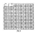
- FIG. 3 shows an arrangement of cells on a semiconductor wafer as shown in FIGS. 2 and 2A are shown.
- the cells are arranged in columns and this over the entire semiconductor die, with the exception of the edge regions which are required for external cells (not shown), which are to be understood as driver stages, input stages and supply lines.
- the unit cell is outlined in FIG. 3. Hundreds of these cells are arranged in column arrangements on the semiconductor die. Currently, more than 1900 such cells are manufactured on a single semiconductor chip, the dimensions of which are 3.8 x 3.8 mm. Each cell is about 0.1 to 0.13 mm long and 0.03 - 0.05 mm wide. In Fig. 3 the cells are not wired and therefore cannot work as active circuits.
- each circuit cell can be considered as a whole or as two cells, which are divided into an active and a wiring cell. This is explained in more detail below.
- the resistor RB is connected once to the base electrode of the associated transistor T1 and then to a voltage source + V.
- the resistor RC is connected once to the assigned collector electrode and to + V.
- the emitter of each transistor is also connected to ground potential.
- FIG. 4 shows part of a semiconductor die which is wired in accordance with the invention.
- the arrangement of five columns C1-C5 and 11 rows R1-R11 shows the part of a semiconductor die which can perform the logic macro function of an input line selector, similar to a decoder.
- This macro takes in operation circuit on signals coming from the input stages of the semiconductor chip, decodes these signals and transmits them according to various other macros within the semiconductor chip.
- the dashed lines that run perpendicular to the longitudinal direction of the cells and parallel to the direction of the column arrangement are conductors formed over the first insulating layer 31 over the active regions of the semiconductor die.
- the solid parallel lines, generally along the length of the cells and perpendicular to the first level leads, are conductors made on the second insulating layer 34 overlying the first level leads.
- Contacts between the first level conductors and selected active semiconductor zones within the cells are made through holes or openings in the first insulating layer, which are represented by filled squares, such as. B. indicated at 100.
- the active zones in this example are the base and collector of the transistor and the diodes in each of the cells.
- cells that have to perform other circuit functions such as. B. TTL, ECL etc. be the active zones of other types of doped zones. Since in this preferred circuit cell Emitters of the transistors and both resistors are wired for each active cell, these contacts are not shown for clarity.
- contact connections are not made directly by conductors of the second metallization level after the active zones.
- a conductor of the second metallization level is first connected to a conductor of the first metallization level via a through hole in the second insulation layer.
- This conductor of the first metallization level then establishes a connection to the active zone via a metallized hole in the first insulating layer. This is shown at 102 in FIG. 4, for example.
- the line is indicated by an oblique line, as at 103 in FIG . 4.
- the conductor of the second metallization level lies directly above the conductor of the first metallization level and is only separated from it by the second insulating layer.
- the second insulation layer separates the two from one another, as shown at 104.
- the first insulating layer 31 generally consists of a double layer of silicon dioxide and silicon nitride. Of course, other dielectric layers could be used as the first insulating layer with equally good results.
- the first level of metallization which produces both the ohmic contacts after the doped zones of the transistor and the non-ohmic contacts after the Schottky junction diodes, consists of a first chrome layer with a thickness of approximately 0.1 micron, a platinum layer deposited thereon followed by an aluminum layer or a layer of an aluminum-copper alloy and silicon. Other types of metallization can also be used.
- the Schottky junction diode contact for Schottky junction diodes with a potential threshold of approximately 0.5 eV preferably consists of a layer of tantalum and a layer of chromium, over which the aluminum metallization lies.
- Aluminum forms the first level of metallization of connecting lines and is manufactured using standard mask and etching processes.
- the second insulation layer 34 for example made of quartz, is deposited and thus provides insulation between the already existing first metallization level and the second metallization level. Through bores are made in the insulating layer 34 made of quartz or glass at the points where connections between the second metallization level and the first level of metallization are to be produced.
- the entire last line R11 is provided exclusively for the wiring of the second metallization level and thus forms a global wiring between the macro shown and other macros not shown.
- no active zones of a cell within the substrate in row 11 and columns C1-C5 along that row are contacted by wirings of the first or second level of metallization.
- all other cells within this macro except R10 / C3 are used as active circuits. Connections are thus made from the wiring of the first metallization level to at least one active zone of each cell, which is not used exclusively for wiring.
- Each of the conductors of the second metallization level in row R11 is connected to the collector of an associated transistor in the cells of row R10 via a line of the first metallization level, such as. B. at 105. Therefore, the conductors of the first and second metallization levels in R11 form part of a macro consisting of 5 ⁇ 11 cells, but are located in areas that do not contain any exposed active cells. This represents a highly effective wiring system, since in the other case the wiring would be interrupted by other wiring connected to active zones, as a result of which wiring routing around the cells would have to be provided in this wiring.
- each cell is designated either with A as the active cell or W as the wiring cell.
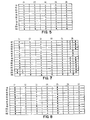
- FIG. 6 shows a somewhat more complex macro circuit which shows 6 columns with 15 cells each for a total of 90 such cells.
- This macro is a 4-bit address register with true and complementary output signals and parity bit generators.
- the essential aspect of this arrangement is the use of cells both as active cells and as wiring cells.
- the left side of cell 106 located in column C1 and row R14 is used only for the wiring of the first level.
- This group of lines is arranged in a region of the cells in column C1 that are not exposed. None of the Schottky diode inputs on the left side of the circuit cells at locations C1 / R13 and R14 are connected to the wiring, although on the other hand only the right side of these cells are used as active cells.
- the remaining cells in this column are only used for the wiring. In column 1, therefore, a complete wiring channel of the first metallization level runs through the macro. A similar channel is available in column C6.
- Fig. 7 shows in a simplified form the arrangement, where in addition to a continuous arrangement of wiring cells on the circumference or at the edge of the macro also individual wiring cells within the macro can be seen, for example with C3 / R6, C3 / R7 and C3 / R8.
- FIG. 8 shows the schematic arrangement of a macro in which the wiring of the second metallization level in an entire row R9 runs across the entire macro.
- the wiring of the first metallization level in column C5 provides a similar wiring channel for signal lines connected in columns through the macro. All active cells are fully utilized and the global wiring cannot go through the active cells. By allowing interconnect cables to pass through the macro rather than around the macro, the length of the wiring is reduced, with further advantages being less space and voltage drops.
- the circuit density on modern semiconductor dies is limited by the wiring required to interconnect the circuit cells.
- Most circuit designs require that a greater density of leads be provided near the center of the die than at the periphery.
- the present invention allows a greater wiring density in the center of the die compared to the circumference and also allows other solutions for the arrangement of cells on the entire die.
- the wiring cells have the same area as the active cells as in the previous embodiments with respect to macros, and there are more wiring cells of the same area in the middle of the Semiconductor wafer arranged as on the circumference. As a result, a larger number of lines can be provided in the vicinity of the center point of the semiconductor die.
- each wiring cell is selected differently, so that the area of an individual wiring cell in the center of the semiconductor die is larger than the area of a wiring cell on the circumference.
- various modifications to this arrangement are possible and would still fall within the scope of the invention.
- the wiring cells shown in FIGS. 9 and 10 are intended for the first metallization level of the wiring, but this arrangement can be used in exactly the same way for the orthogonal wiring of the second metallization level.
Landscapes
- Design And Manufacture Of Integrated Circuits (AREA)
- Semiconductor Integrated Circuits (AREA)
- Internal Circuitry In Semiconductor Integrated Circuit Devices (AREA)
Applications Claiming Priority (2)
| Application Number | Priority Date | Filing Date | Title |
|---|---|---|---|
| US83071577A | 1977-09-06 | 1977-09-06 | |
| US830715 | 1992-02-04 |
Publications (1)
| Publication Number | Publication Date |
|---|---|
| EP0001209A1 true EP0001209A1 (fr) | 1979-04-04 |
Family
ID=25257547
Family Applications (1)
| Application Number | Title | Priority Date | Filing Date |
|---|---|---|---|
| EP78100654A Withdrawn EP0001209A1 (fr) | 1977-09-06 | 1978-08-16 | Circuit semi-conducteur intégré |
Country Status (5)
| Country | Link |
|---|---|
| US (1) | UST100501I4 (fr) |
| EP (1) | EP0001209A1 (fr) |
| JP (1) | JPS5441088A (fr) |
| CA (1) | CA1102009A (fr) |
| IT (1) | IT1110167B (fr) |
Cited By (7)
| Publication number | Priority date | Publication date | Assignee | Title |
|---|---|---|---|---|
| EP0005723A1 (fr) * | 1978-05-25 | 1979-12-12 | International Business Machines Corporation | Circuit intégré à grande échelle et son procédé de fabrication |
| EP0021661A1 (fr) * | 1979-06-07 | 1981-01-07 | Fujitsu Limited | Dispositif semiconducteur du type "masterslice" |
| FR2524206A1 (fr) * | 1982-03-26 | 1983-09-30 | Thomson Csf Mat Tel | Circuit integre prediffuse, et procede d'interconnexion des cellules de ce circuit |
| EP0151267A1 (fr) * | 1983-12-30 | 1985-08-14 | International Business Machines Corporation | Circuit à très grande intégration à haute densité |
| EP0154346A3 (en) * | 1984-03-08 | 1986-10-08 | Kabushiki Kaisha Toshiba | Semiconductor integrated circuit configurated by using polycell technique |
| US4737836A (en) * | 1983-12-30 | 1988-04-12 | International Business Machines Corporation | VLSI integrated circuit having parallel bonding areas |
| DE4124877A1 (de) * | 1990-07-27 | 1992-02-20 | Mitsubishi Electric Corp | Integrierte halbleiterschaltungsvorrichtung und verfahren zum anordnen und verdrahten von zellen |
Families Citing this family (6)
| Publication number | Priority date | Publication date | Assignee | Title |
|---|---|---|---|---|
| JPS55138865A (en) * | 1979-04-17 | 1980-10-30 | Nec Corp | Semiconductor device |
| US4623911A (en) | 1983-12-16 | 1986-11-18 | Rca Corporation | High circuit density ICs |
| JPS61241964A (ja) | 1985-04-19 | 1986-10-28 | Hitachi Ltd | 半導体装置 |
| JPS6288337A (ja) * | 1985-10-15 | 1987-04-22 | Nec Corp | 半導体集積回路装置 |
| JP2685756B2 (ja) * | 1987-07-20 | 1997-12-03 | 株式会社東芝 | 半導体集積回路装置の設計方法 |
| US10878158B2 (en) * | 2018-07-16 | 2020-12-29 | Taiwan Semiconductor Manufacturing Company, Ltd. | Semiconductor device including cell region having more similar cell densities in different height rows, and method and system for generating layout diagram of same |
Citations (3)
| Publication number | Priority date | Publication date | Assignee | Title |
|---|---|---|---|---|
| GB1443363A (en) * | 1972-07-10 | 1976-07-21 | Amdahl Corp | Methode of manufacturing lsi chips |
| CH583970A5 (fr) * | 1974-06-26 | 1977-01-14 | Ibm | |
| DE2659246A1 (de) * | 1975-12-29 | 1977-07-07 | Fujitsu Ltd | Halbleitervorrichtung |
Family Cites Families (1)
| Publication number | Priority date | Publication date | Assignee | Title |
|---|---|---|---|---|
| US4006492A (en) * | 1975-06-23 | 1977-02-01 | International Business Machines Corporation | High density semiconductor chip organization |
-
1978
- 1978-06-14 CA CA305,463A patent/CA1102009A/fr not_active Expired
- 1978-07-25 JP JP9006178A patent/JPS5441088A/ja active Pending
- 1978-08-16 EP EP78100654A patent/EP0001209A1/fr not_active Withdrawn
- 1978-08-25 IT IT27013/78A patent/IT1110167B/it active
-
1979
- 1979-07-17 US US06/058,360 patent/UST100501I4/en active Pending
Patent Citations (3)
| Publication number | Priority date | Publication date | Assignee | Title |
|---|---|---|---|---|
| GB1443363A (en) * | 1972-07-10 | 1976-07-21 | Amdahl Corp | Methode of manufacturing lsi chips |
| CH583970A5 (fr) * | 1974-06-26 | 1977-01-14 | Ibm | |
| DE2659246A1 (de) * | 1975-12-29 | 1977-07-07 | Fujitsu Ltd | Halbleitervorrichtung |
Non-Patent Citations (3)
| Title |
|---|
| ELECTRONICS, Band 42, nr. 2, 20 Januar 1969, New York. P.E. RODLEY: "Metallization is designed quickly and inexpensively", Seiten 78-81 * |
| IBM TECHNICAL DISCLOSURE BULLETIN, Band 20, nr. 1, Juni 1977, New York. B.C. FOX et al: "Slotted macro design structure"; Seiten 186-188 * |
| IBM TECHNICAL DISCLOSURE BULLETIN, Band 20, nr. 2, Juli 1977, New York. J.Z. CHEN et al: "Off-chip groundup receiver", Seiten 613-614 * |
Cited By (10)
| Publication number | Priority date | Publication date | Assignee | Title |
|---|---|---|---|---|
| EP0005723A1 (fr) * | 1978-05-25 | 1979-12-12 | International Business Machines Corporation | Circuit intégré à grande échelle et son procédé de fabrication |
| EP0021661A1 (fr) * | 1979-06-07 | 1981-01-07 | Fujitsu Limited | Dispositif semiconducteur du type "masterslice" |
| FR2524206A1 (fr) * | 1982-03-26 | 1983-09-30 | Thomson Csf Mat Tel | Circuit integre prediffuse, et procede d'interconnexion des cellules de ce circuit |
| EP0090704A1 (fr) * | 1982-03-26 | 1983-10-05 | Thomson-Csf Telephone | Circuit intégré prédiffusé, et procédé d'interconnexion des cellules de ce circuit |
| US4644382A (en) * | 1982-03-26 | 1987-02-17 | Thomson-Csf Telephone | Prediffused integrated circuit and a method of interconnection of the cells of said circuit |
| EP0151267A1 (fr) * | 1983-12-30 | 1985-08-14 | International Business Machines Corporation | Circuit à très grande intégration à haute densité |
| US4737836A (en) * | 1983-12-30 | 1988-04-12 | International Business Machines Corporation | VLSI integrated circuit having parallel bonding areas |
| EP0154346A3 (en) * | 1984-03-08 | 1986-10-08 | Kabushiki Kaisha Toshiba | Semiconductor integrated circuit configurated by using polycell technique |
| DE4124877A1 (de) * | 1990-07-27 | 1992-02-20 | Mitsubishi Electric Corp | Integrierte halbleiterschaltungsvorrichtung und verfahren zum anordnen und verdrahten von zellen |
| US6121644A (en) * | 1990-07-27 | 2000-09-19 | Mitsubishi Denki Kabushiki Kaisha | Semiconductor integrated circuit device and method of arranging and wiring cells |
Also Published As
| Publication number | Publication date |
|---|---|
| IT1110167B (it) | 1985-12-23 |
| UST100501I4 (en) | 1981-04-07 |
| JPS5441088A (en) | 1979-03-31 |
| CA1102009A (fr) | 1981-05-26 |
| IT7827013A0 (it) | 1978-08-25 |
Similar Documents
| Publication | Publication Date | Title |
|---|---|---|
| EP0005723B1 (fr) | Circuit intégré à grande échelle et son procédé de fabrication | |
| DE69524804T2 (de) | Basiszelle für BICMOS und CMOS-Gate-Arrays | |
| DE2542518C3 (fr) | ||
| DE2826847C2 (de) | Hochintegrierte Halbleiterschaltungsanordnung | |
| DE2334405B2 (de) | Hochintegrierte (LSI-) Halbleiterschaltung und Verfahren zur Herstellung einer Vielzahl derartiger Halbleiterschaltungen | |
| DE68919636T2 (de) | Ununterbrochene Matrix, deren Plattengrösse programmierbar ist. | |
| DE3781469T2 (de) | Integrierte halbleiter-schaltung mit einer verbesserten verbindungsstruktur. | |
| DE69031603T2 (de) | Integrierter Torschaltungs-Schaltkreis | |
| DE3223276A1 (de) | Integrierte halbleiterschaltung und verfahren zu ihrer herstellung | |
| DE69132984T2 (de) | Programmierbare Verbindungsarchitektur | |
| DE3427285C2 (fr) | ||
| DE3423211C2 (de) | Halbleiterbauteil | |
| DE3586385T2 (de) | Integrierte gate-matrixstruktur. | |
| DE2627546A1 (de) | Integrierte schaltung hoher packungsdichte | |
| DE2556274A1 (de) | Logische schaltung hoher schaltungsdichte | |
| DE2655575A1 (de) | Kompakte monolithische halbleiterstruktur | |
| DE68928193T2 (de) | Halbleiterchip und Verfahren zu seiner Herstellung | |
| EP0001209A1 (fr) | Circuit semi-conducteur intégré | |
| DE2523221C2 (fr) | ||
| DE2556668C3 (de) | Halbleiter-Speichervorrichtung | |
| DE3927143C2 (de) | Gate-Array | |
| DE3751607T2 (de) | Stromversorgungsleitungen in einer integrierten Halbleiterschaltung. | |
| DE1764567B2 (de) | Integrierte schaltung mit auflagen auf unbenuetzten, aktiven flaechenschaltelementen | |
| DE1616438C3 (de) | Integrierte Schaltung, Verwendung dieser Schaltung und Verfahren zu ihrer Herstellung | |
| DE3147932A1 (de) | "anordnung mit integrierten schaltungen hoher integrationsdichte |
Legal Events
| Date | Code | Title | Description |
|---|---|---|---|
| PUAI | Public reference made under article 153(3) epc to a published international application that has entered the european phase |
Free format text: ORIGINAL CODE: 0009012 |
|
| AK | Designated contracting states |
Designated state(s): DE FR GB |
|
| 17P | Request for examination filed | ||
| STAA | Information on the status of an ep patent application or granted ep patent |
Free format text: STATUS: THE APPLICATION HAS BEEN WITHDRAWN |
|
| 18W | Application withdrawn | ||
| RIN1 | Information on inventor provided before grant (corrected) |
Inventor name: GRUODIS, ALGIRDAS JOSEPH Inventor name: BALYOZ, JOHN |