EP0013603A1 - Verbesserter Festwertspeicher und Programmierverfahren für diesen Speicher - Google Patents
Verbesserter Festwertspeicher und Programmierverfahren für diesen Speicher Download PDFInfo
- Publication number
- EP0013603A1 EP0013603A1 EP80300034A EP80300034A EP0013603A1 EP 0013603 A1 EP0013603 A1 EP 0013603A1 EP 80300034 A EP80300034 A EP 80300034A EP 80300034 A EP80300034 A EP 80300034A EP 0013603 A1 EP0013603 A1 EP 0013603A1
- Authority
- EP
- European Patent Office
- Prior art keywords
- lines
- layer
- regions
- memory
- conductive lines
- Prior art date
- Legal status (The legal status is an assumption and is not a legal conclusion. Google has not performed a legal analysis and makes no representation as to the accuracy of the status listed.)
- Granted
Links
Images

Classifications
-
- H—ELECTRICITY
- H10—SEMICONDUCTOR DEVICES; ELECTRIC SOLID-STATE DEVICES NOT OTHERWISE PROVIDED FOR
- H10D—INORGANIC ELECTRIC SEMICONDUCTOR DEVICES
- H10D88/00—Three-dimensional [3D] integrated devices
-
- G—PHYSICS
- G11—INFORMATION STORAGE
- G11C—STATIC STORES
- G11C17/00—Read-only memories programmable only once; Semi-permanent stores, e.g. manually-replaceable information cards
- G11C17/08—Read-only memories programmable only once; Semi-permanent stores, e.g. manually-replaceable information cards using semiconductor devices, e.g. bipolar elements
-
- G—PHYSICS
- G11—INFORMATION STORAGE
- G11C—STATIC STORES
- G11C17/00—Read-only memories programmable only once; Semi-permanent stores, e.g. manually-replaceable information cards
- G11C17/14—Read-only memories programmable only once; Semi-permanent stores, e.g. manually-replaceable information cards in which contents are determined by selectively establishing, breaking or modifying connecting links by permanently altering the state of coupling elements, e.g. PROM
-
- H—ELECTRICITY
- H10—SEMICONDUCTOR DEVICES; ELECTRIC SOLID-STATE DEVICES NOT OTHERWISE PROVIDED FOR
- H10P—GENERIC PROCESSES OR APPARATUS FOR THE MANUFACTURE OR TREATMENT OF DEVICES COVERED BY CLASS H10
- H10P34/00—Irradiation with electromagnetic or particle radiation of wafers, substrates or parts of devices
- H10P34/40—Irradiation with electromagnetic or particle radiation of wafers, substrates or parts of devices with high-energy radiation
- H10P34/42—Irradiation with electromagnetic or particle radiation of wafers, substrates or parts of devices with high-energy radiation with electromagnetic radiation, e.g. laser annealing
Definitions
- This invention relates generally to semiconductor devices and integrated circuits, and more particularly the invention relates to programmable read only memories and the method of programming a read only memory.
- a read only memory comprises a plurality of X lines and a plurality of Y lines which are selectively addressed to read stored bits of information.
- the X lines and Y lines are selectively interconnected by diodes to define stored bits of information.
- the stored information defined by a current path between the addressed lines (e.g. a "1") or lack thereof (e.g. a "zero"), can be detected.
- Semiconductor ROM's are known which can be programmed after fabrication by the application of high voltages to render selected transistor components conductive.
- Laser coding has been proposed, also. North and Weick in "Laser Coding of Bipolar Read Only Memories" IEEE Journal of Solid State Circuits, Vol. SC-11, No. 4, August, 197G, pp. 500-505 propose the coding of high speed bipolar silicon integrated circuit memories by the selective vaporization of metal links connecting contact pads of each memory cell to metal bit lines. By vaporizing the conductive link, current paths are interrupted to define the stored code.
- an aluminum conductor is placed over a contact region of an underlying semiconductor substrate with a thin layer of silicon oxide therebetween.
- a laser beam is applied to open the aluminum layer with material being removed by vaporization.
- the silicon oxide insulating layer is removed by controlled microexplosion caused by thermal stress and/or vaporization of material at the silicon oxide-silicon interface.
- a conducting path is formed by flow of molten silicon into contact with the aluminum.
- An object of the present invention is an improved programmable read only memory.
- Another object of the invention is an improved method of programming a read only memory by selective radiation.
- Still another object of the invention is a programmable read only memory which is readily fabricated as part of an integrated circuit or on top thereof.
- Yet another object of the invention is an integrated circuit including read only memory which is readily programmed after fabrication.
- a programmable read only memory in accordance with the present invention includes a first plurality of spaced parallel conductive lines on a surface of a support means and a layer of polycrystalline semiconductor material includes doped regions extending partially through the layer with each region being positioned above a line of the first plurality of conductive lines.
- a second plurality of conductive lines is provided on the surface of the layer of polycrystalline semiconductor material with the second plurality of conductive lines being skewed with respect to the first plurality of conductive lines.
- the regions of doped material are provided at cross points of the first plurality' of lines and the second plurality of conductive lines, and the first plurality of lines and second plurality of lines are selectively interconnected by applying a radiation beam to selected ones of the doped regions to diffuse dopant atoms to the conductive line thereunder and thus provide diode current paths between the first plurality of lines and second plurality of lines.
- no vaporizing of material results therefrom.
- the read only memory can be fabricated on the surface of an integrated circuit and interconnected therewith to become a part thereof. Additional memory layers can be added resulting in a compact multilay-r structure.
- a radiation beam such as a laser or electron beam is directed on a doped region with sufficient energy to cause local diffusion, with or without melting,of dopants to the underlying line and thereby interconnect the first line to the second line, but without physically damaging the structure.
- the doped regions can be formed by ion implantation with the doped regions extending substantially to the underlying conductive lines. Thereafter, by application of a radiation beam'selected implanted regions are activated to form diodes connected between X and Y lines.
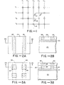
- Figure 1 illustrates schematically a read only memory which includes a plurality of first conductive lines, designated the X lines (Xl-X5), and a second plurality of conductive lines designated the Y lines (Y1-Y4).
- the first plurality of lines is skewed with respect to the second plurality of lines with the intersection of lines either being interconnected through diodes as shown or not connected as illustrated by circles.
- the memory is read by applying a voltage potential between an X line and a Y line and detecting the presence or absence of a current. When no connection is made between the lines, the absence of a current may signify a binary "O".
- a connection when a connection is made between the two lines the presence of a current may signify a binary "1". For example by applying a negative voltage to the X3 line and groundino the Y2 line, a current flowing from the Y2 line through diode 12 to the X3 line is detected. Similarly, by applying the negative voltage to the X3 line and grounding the Y3 line a current flowing from the Y3 line through diode 14 to the X3 line can be detected. However, with the negative voltage on the X3 line and the Y4 line grounded no current flows due to no connection being made'between the Y4 and X3 lines, as designated by circle 16.
- the memory array By addressing the memory array through energization of selected X lines and Y lines, stored data or binary bits can be read out by detecting the presence or absence of a current. It will be appreciated that the array can include thousands of lines and thousands of bits of stored data.
- a read only memory array It is advantageous to fabricate a memory array and retain the capability of programming the memory after completion of the array. Moreover, it would be advantageous to incorporate such a read only memory in a monolithic integrated circuit or other microminiature electrical system. Conventional read only memories typically do not include other circuitry and most are preprogrammed during fabrication. However, a read only memory in accordance with the present invention is readily fabricated at part of an integrated circuit or other electronic array and may be programmed after fabrication.
- FIG. 2(A & B) the fabrication and programming of a read only memory in accordance with the present invention is illustrated in one embodiment.
- FIG A the plan view of a portion of a ROM is illustrated in Figure A
- Figure B a section view of the portion of the ROM shown in Figure A is illustrated in Figure B.
- a semiconductor substrate 20 of silicon for example, is provided with a silicon oxide layer 22 on a major surface thereof, and a layer of polycrystalline silicon 24 is formed on the surface of silicon oxide layer 22.
- Substrate 20 may comprise a part of an integrated circuit, or the substrate may be of other suitable material such as polycrystalline silicon or glass which has been deposited on a circuit array or the like to accommodate the read only memory.
- Silicon oxide layer 22 may be typically on the order of 1000 angstroms in thickness to provide electrical insulation and also a suitable surface for the vapor deposition of polycrystalline silicon or like material.
- the polycrystalline silicon material 24 may be formed by vapor deposition in a suitable reactor to a thickness on the order of 0.5 micron, and a plurality of spaced parallel conductive lines 26 are formed therein by diffusion or ion implantation techniques.
- arsenic may be implanted with a concentration of 5 x 10 15 ions per square centimeter at a potential 170 kev, for example.
- the doped polycrystalline silicon is preferably annealed either in an oven at an elevated temperature (e.g.
- a second layer of polycrystalline silicon material 28 is formed on the first layer 24 by vapor deposition with the thickness of layer 28 being on the order of 0.5 micron.
- a plurality of rectanu- larly shaped, P type doped regions 30 are formed in surface regions of layer 28, for example, by implanting boron ions in a density of 5 x 10 14 ions per square centimeter at 100 kev.
- the shallow regions 30 do not extend completely through layer 28 and thus are spaced from the underlying conductive line 26.
- each of the regions 30 is generally rectangular in shape and is positioned above a conductive line 26 in the underlying polycrystalline layer.
- a second plurality of conductive lines 32 are formed on the surface of layer 28 in alignment with the diffused regions 30 and skewed with respect to the underlying plurality of lines 26.
- Lines 32 may be formed by sputtering or vapor deposition and selective etching of suitable metal such as aluminum, or alternatively the lines may be formed by doping of the surface of polycrystalline silicon layer 28.
- the width of lines 32 are substantially less than the length of the rectangular regions 30.
- the programming of the read only memory is accomplished by applying a laser beam on a generally circular surface area 34 which overlaps a region 30 but preferably is spaced from the metal lead 32.
- the P type ions diffuse through layer 28 and into contact with the underlying N type region of layer 24 which defines line 26.
- a Piv junction, or diode is formed which interconnects metal layer 32 to the underlying line 26.
- the first plurality of lines can be selectively interconnected with the second plurality of lines by application of a laser beam and diffusion of the P type impurities in the radiated region 30 to the underlying line.
- the radiation beam need not contact the metal lines 32, and no melting of the metal in the lines results.
- the invention can be practiced by applying the laser beam directly to the line 32 to cause diffusion of impurities in the region 30 immediately underlying the laser beam and the metal line.
- the second plurality of lines are defined by doped polycrystalline material, application of the laser beam likely would have no deleterious effects by being applied directly thereto. Closer spacing of the second plurality of lines can then be effected.
- the memory can be programmed prior to application of the second plurality of lines by radiation aided diffusion of impurities in selectee regions 30 prior to the definition of the second plurality of lines. Such a procedure may be preferred if later programming of the ROM is not required.
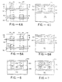
- ion implanted regions can be employed, as illustrated in Figures 6 and 7.
- a silicon substrate 120 has a layer 122 of silicon oxide on one surface with a polycrystalline silicon layer 124 formed thereon.
- the first set of lines 126 are formed in layer 124 and a second polycrystalline silicon layer 130 is formed thereover.
- Regions 132 are formed by ion implantation with the regions extending substantially through layer 124. Assuming that the lines 126 are N type conductivity, the regions 132 are P type.
- a second set of lines are formed over layer 130 such as illustrated by a metal line 134 such as tungsten.
- implanted ions must be activated by annealing.
- Selective annealing where a binary "1" is wished to be written, can be done with a radiation beam either through the metal 134 or on the side of the metal line.
- the implanted region 132 diode interconnections between line 134 and the lines 126 can be created by activating a P type region 132 which then forms a P-N junction with the underlying N type region 126.
- the annealing of the implanted region can be done selectively by laser irradiation and at a lower temperature than is required for melting. See, for example, Gat, Gerzberg, Gibbons et al "cw Laser Anneal of Polycrystalline Silicon: Crystalline Structure, Electrical Properties", Applied Physics Letters, October 15, 1978.
- Figure 7 is a cross-section of a portion of a device similar to that illustrated in Figure 6, but in this embodiment an N type region 131 is implanted in the layer 130 and then the P type region 132 is implanted thereover. Upon activation of the regions 131 and 132 by annealing, the P-N junction of the interconnecting diode is located at the interface of the regions 131, 132.
- regions 132 in Figure 6 and regions 131, 132 in Figure 7, as well as the regions 30 in Figure 3, may comprise a continuous, ion-implanted layer. Prior to annealing the layer is substantially non-conductive. Only at the locations of irradiation and ion diffusion or annealing does the layer become conductive.
- a programmable read only memory in accordance with the present invention is readily fabricated with an integrated circuit array as illustrated in the section views of Figure 8 and Figure 9 of portions of integrated circuits.
- a portion of the ROM is illustrated above a silicon gate field effect transistor shown generally at 40 which includes a source 42, drain 44, and a gate electrode 46.
- the metal interconnects 48 to the source and drain regions are formed over field oxide 49 and are covered with a silicon oxide layer 50, and the read only memory structure is formed on the insulating silicon oxide layer 50.
- a first plurality of lines are provided in a first polycrystalline silicon layer 52 which is formed directly on silicon oxide layer 50, and the second polycrystalline silicon layer 54 is formed on layer J2 with a second line defined by metal layer 56 on polysilicon 54.
- Selective interconnection of line 56 to lines in the underlying polycrystalline silicon layer 52 is accomplished by applying a radiation beam to selected regions 58 to diffuse dopants therein into engagement with lines in the first polycrystalline silicon layer 52.
- FIG. 9 A similar cross section view is illustrated in Figure 9 of a portion of an integrated circuit which includes a bipolar junction transistor 60 including emitter 62, base 64 and collector 66.
- Metal leads 68 are provided to the collector and emitter, respectively, and the leads are covered by an insulating layer of silicon oxide 70.
- the read only memory is formed directly thereover including a first polycrystalline silicon layer 72, a second polycrystalline silicon layer 74, metal layer 76, and the regions 78 which selectively interconnect metal layer 76 to lines in.layer 72 by means of application of a laser beam.
- a read only memory in accordance with the present invention not only can be incorporated as part of an integrated circuit, the array can be fabricated directly on a circuit assembly as shown in Figure 10 which illustrates a perspective view of a microprocessor circuit board.
- the microprocessor is incorporated in a large scale integrated chip which is mounted on a frame 92 along with suitable processor I/O circuitry 94.
- the microprocessor LSI chip is coated with a suitable insulating material such as glass or epoxy, and a read only memory array 96 is then formed over the LSI chip.
- the Y lines of the ROM are connected to a Y MUX 98, and the X lines of the ROM are connected to an X MUX 99.
- programming of the ROM can be effected after completion of the electrical assembly by selectively irradiating the ROM to effect interconnection of selected X and Y lines and thus record binary data.
- the first and second plurality of lines can be fabricated from metal, doped polycrystalline silicon, or other suitable conductive material. While interconnection of the lines is preferably accomplished by applying a radiation beam to a surface area adjacent to the top conductive line and thus avoiding physical alternation of the line, the radiation beam can be applied directly to the line thus allowing higher density assembly of the ROM structure. While a laser beam has been described for effecting the diffusion of dopant impurities, other radiation beams such as an electron beam could be utilized.
- the ROM can be programmed during fabrication and prior to formation of the second plurality of lines if so desired. Further, the ROM may comprise multiple layers of address lines in a stacked array thus providing greater storage capacity in the same surface area.
Landscapes
- Semiconductor Memories (AREA)
- Read Only Memory (AREA)
Applications Claiming Priority (2)
| Application Number | Priority Date | Filing Date | Title |
|---|---|---|---|
| US06/001,360 US4233671A (en) | 1979-01-05 | 1979-01-05 | Read only memory and integrated circuit and method of programming by laser means |
| US1360 | 2001-10-23 |
Publications (2)
| Publication Number | Publication Date |
|---|---|
| EP0013603A1 true EP0013603A1 (de) | 1980-07-23 |
| EP0013603B1 EP0013603B1 (de) | 1983-05-18 |
Family
ID=21695648
Family Applications (1)
| Application Number | Title | Priority Date | Filing Date |
|---|---|---|---|
| EP80300034A Expired EP0013603B1 (de) | 1979-01-05 | 1980-01-04 | Verbesserter Festwertspeicher und Programmierverfahren für diesen Speicher |
Country Status (5)
| Country | Link |
|---|---|
| US (1) | US4233671A (de) |
| EP (1) | EP0013603B1 (de) |
| JP (1) | JPS5593254A (de) |
| CA (1) | CA1137630A (de) |
| DE (1) | DE3063206D1 (de) |
Cited By (4)
| Publication number | Priority date | Publication date | Assignee | Title |
|---|---|---|---|---|
| EP0058748A1 (de) * | 1981-02-23 | 1982-09-01 | BURROUGHS CORPORATION (a Delaware corporation) | Auf einem Halbleitersubstrat angebrachter maskenprogrammierbarer Festwertspeicher |
| EP0061602A1 (de) * | 1981-03-27 | 1982-10-06 | International Business Machines Corporation | Eine Methode zur Herstellung und zum Testen einer programmierbaren integrierten Schaltung vor ihrer Programmierung |
| FR2520146A1 (fr) * | 1982-01-15 | 1983-07-22 | Thomson Csf | Matrice d'elements a memoire integres, a diode schottky sur silicium polycristallin, et procede de fabrication |
| GB2167621A (en) * | 1984-11-27 | 1986-05-29 | Crystalate Electronics | Programmed matrix device |
Families Citing this family (30)
| Publication number | Priority date | Publication date | Assignee | Title |
|---|---|---|---|---|
| JPS5750467A (en) * | 1980-09-12 | 1982-03-24 | Fujitsu Ltd | Semiconductor memory |
| JPS5750468A (en) * | 1980-09-12 | 1982-03-24 | Fujitsu Ltd | Semiconductor memory |
| JPS58188155A (ja) * | 1982-04-27 | 1983-11-02 | Seiko Epson Corp | 2層構造rom集積回路 |
| JPS58209157A (ja) * | 1982-05-31 | 1983-12-06 | Seiko Epson Corp | 半導体記憶素子 |
| JPS60245164A (ja) * | 1984-05-18 | 1985-12-04 | Fujitsu Ltd | ダイオ−ドアレイの製造方法 |
| US5679967A (en) * | 1985-01-20 | 1997-10-21 | Chip Express (Israel) Ltd. | Customizable three metal layer gate array devices |
| US4924287A (en) * | 1985-01-20 | 1990-05-08 | Avner Pdahtzur | Personalizable CMOS gate array device and technique |
| IL86162A (en) * | 1988-04-25 | 1991-11-21 | Zvi Orbach | Customizable semiconductor devices |
| US5545904A (en) * | 1986-01-17 | 1996-08-13 | Quick Technologies Ltd. | Personalizable gate array devices |
| US5329152A (en) * | 1986-11-26 | 1994-07-12 | Quick Technologies Ltd. | Ablative etch resistant coating for laser personalization of integrated circuits |
| IL82113A (en) * | 1987-04-05 | 1992-08-18 | Zvi Orbach | Fabrication of customized integrated circuits |
| DE3731621A1 (de) * | 1987-09-19 | 1989-03-30 | Texas Instruments Deutschland | Verfahren zum herstellen einer elektrisch programmierbaren integrierten schaltung |
| US4929995A (en) * | 1988-02-16 | 1990-05-29 | Honeywell Inc. | Selective integrated circuit interconnection |
| JP2778977B2 (ja) * | 1989-03-14 | 1998-07-23 | 株式会社東芝 | 半導体装置及びその製造方法 |
| JPH03225868A (ja) * | 1990-01-30 | 1991-10-04 | Hitachi Ltd | 固体撮像素子とそれを用いた撮像装置 |
| JPH0461162A (ja) * | 1990-06-22 | 1992-02-27 | Mitsubishi Electric Corp | 半導体集積回路装置 |
| JPH04115565A (ja) * | 1990-09-05 | 1992-04-16 | Mitsubishi Electric Corp | 半導体記憶装置 |
| GB9113795D0 (en) * | 1991-06-26 | 1991-08-14 | Philips Electronic Associated | Thin-film rom devices and their manufacture |
| US5811869A (en) * | 1996-01-04 | 1998-09-22 | Micron Technology, Inc. | Laser antifuse using gate capacitor |
| IL116792A (en) * | 1996-01-16 | 2000-01-31 | Chip Express Israel Ltd | Customizable integrated circuit device |
| US5742555A (en) | 1996-08-20 | 1998-04-21 | Micron Technology, Inc. | Method of anti-fuse repair |
| TW306005B (en) * | 1996-11-22 | 1997-05-21 | United Microelectronics Corp | Decoding method of diode-type read only memory array |
| DE19713173C2 (de) * | 1997-03-27 | 2001-02-15 | Siemens Ag | ROM-Speicher |
| US5831893A (en) * | 1997-05-13 | 1998-11-03 | Sipex Corporation | Memory cell |
| KR100263476B1 (ko) * | 1998-03-24 | 2000-09-01 | 김영환 | 가변회로 컨넥터 형성방법 |
| US5885873A (en) * | 1998-04-20 | 1999-03-23 | Texas Instruments--Acer Incorporated | Double coding processes for mask read only memory (ROM) devices |
| US6836000B1 (en) | 2000-03-01 | 2004-12-28 | Micron Technology, Inc. | Antifuse structure and method of use |
| JP4010091B2 (ja) * | 2000-03-23 | 2007-11-21 | セイコーエプソン株式会社 | メモリデバイスおよびその製造方法 |
| US6964906B2 (en) * | 2002-07-02 | 2005-11-15 | International Business Machines Corporation | Programmable element with selectively conductive dopant and method for programming same |
| US7084053B2 (en) * | 2003-09-30 | 2006-08-01 | Intel Corporation | Unidirectionally conductive materials for interconnection |
Family Cites Families (4)
| Publication number | Priority date | Publication date | Assignee | Title |
|---|---|---|---|---|
| US3763476A (en) * | 1972-03-15 | 1973-10-02 | Gen Electric | Method and apparatus for storing and reading out charge in an insulating layer |
| US3860915A (en) * | 1973-06-29 | 1975-01-14 | Geier Karl Heinz | Matrix arrangement for operating optical elements |
| US4032373A (en) * | 1975-10-01 | 1977-06-28 | Ncr Corporation | Method of manufacturing dielectrically isolated semiconductive device |
| US4130891A (en) * | 1977-08-08 | 1978-12-19 | General Electric Company | Methods of gray scale recording and archival memory target produced thereby |
-
1979
- 1979-01-05 US US06/001,360 patent/US4233671A/en not_active Expired - Lifetime
- 1979-12-28 JP JP17390079A patent/JPS5593254A/ja active Pending
-
1980
- 1980-01-04 CA CA000343099A patent/CA1137630A/en not_active Expired
- 1980-01-04 EP EP80300034A patent/EP0013603B1/de not_active Expired
- 1980-01-04 DE DE8080300034T patent/DE3063206D1/de not_active Expired
Non-Patent Citations (4)
| Title |
|---|
| IBM TECHNICAL DISCLOSURE BULLETIN, Vol. 11, No. 2, July 1968, pages 104-105 New York USA JOSHI et al. "Inducing impurity migration in semiconductors by lasers", * Complete article * * |
| IBM TECHNICAL DISCLOSURE BULLETIN, Vol. 15, No. 8, January 1973, pages 2371-2372, New York COOK et al. "Read-only memory fabrication by laser formed connections". * Page 2372, lines 22-41 * * |
| IBM TECHNICAL DISCLOSURE BULLETIN, Vol. 17, No. 1 June 1974, page 248 New York USA D'HEURLE et al. "Lowering the laser formed contact resistance between Al & Si" * Page 248, lines 1-3 * * |
| IBM TECHNICAL DISCLOSURE BULLETIN, Vol. 17, No. 1, June 1974, page 242, New York USA COOK et al. "Chip personalization by shortlaser pulses", * Complete article * * |
Cited By (6)
| Publication number | Priority date | Publication date | Assignee | Title |
|---|---|---|---|---|
| EP0058748A1 (de) * | 1981-02-23 | 1982-09-01 | BURROUGHS CORPORATION (a Delaware corporation) | Auf einem Halbleitersubstrat angebrachter maskenprogrammierbarer Festwertspeicher |
| EP0061602A1 (de) * | 1981-03-27 | 1982-10-06 | International Business Machines Corporation | Eine Methode zur Herstellung und zum Testen einer programmierbaren integrierten Schaltung vor ihrer Programmierung |
| FR2520146A1 (fr) * | 1982-01-15 | 1983-07-22 | Thomson Csf | Matrice d'elements a memoire integres, a diode schottky sur silicium polycristallin, et procede de fabrication |
| EP0084475A3 (de) * | 1982-01-15 | 1983-08-10 | Thomson-Csf | Matrix von integrierten Speicherelementen aus Schottky dioden auf polykristallinem Silizium und Herstellungsverfahren |
| GB2167621A (en) * | 1984-11-27 | 1986-05-29 | Crystalate Electronics | Programmed matrix device |
| EP0183518A3 (de) * | 1984-11-27 | 1988-09-07 | Crystalate Electronics Limited | Programmierte Speicheranordnung |
Also Published As
| Publication number | Publication date |
|---|---|
| CA1137630A (en) | 1982-12-14 |
| US4233671A (en) | 1980-11-11 |
| JPS5593254A (en) | 1980-07-15 |
| EP0013603B1 (de) | 1983-05-18 |
| DE3063206D1 (en) | 1983-07-07 |
Similar Documents
| Publication | Publication Date | Title |
|---|---|---|
| US4233671A (en) | Read only memory and integrated circuit and method of programming by laser means | |
| EP0118158B1 (de) | Programmierbare ROM-Struktur und Verfahren zum Herstellen einer solchen Struktur | |
| US4748490A (en) | Deep polysilicon emitter antifuse memory cell | |
| US4292730A (en) | Method of fabricating mesa bipolar memory cell utilizing epitaxial deposition, substrate removal and special metallization | |
| US4617723A (en) | Method and device for creating an activatable conducting link in a semiconductor device | |
| US4370798A (en) | Interlevel insulator for integrated circuit with implanted resistor element in second-level polycrystalline silicon | |
| US4312046A (en) | Vertical fuse and method of fabrication | |
| US5004701A (en) | Method of forming isolation region in integrated circuit semiconductor device | |
| GB2086654A (en) | Programmable cells and arrays | |
| EP0080730B1 (de) | Halbleiteranordnung mit Verdrahtungsschichten und Verfahren zur Herstellung derselben | |
| EP0051500B1 (de) | Halbleiterbauelement | |
| EP0058124A1 (de) | Anordnung von Schottkydioden aus polykristallinem Silizium und Verfahren zur Herstellung | |
| US3770606A (en) | Schottky barrier diodes as impedance elements and method of making same | |
| EP0172193B1 (de) | Programmierbare nur-lesespeicherzelle und verfahren zum herstellen | |
| US4692787A (en) | Programmable read-only-memory element with polycrystalline silicon layer | |
| US4376984A (en) | Programmable read-only memory device | |
| EP0078220B1 (de) | Polykristalline Silizium-Verbindungen für Bipolartransistoren in Flip-Flop-Schaltung | |
| US4145702A (en) | Electrically programmable read-only-memory device | |
| EP0041770A2 (de) | Programmierbare Nur-Lese-Speichervorrichtung und Herstellungsverfahren | |
| US4247343A (en) | Method of making semiconductor integrated circuits | |
| US5554549A (en) | Salicide process for FETs | |
| US5834811A (en) | Salicide process for FETs | |
| US4404658A (en) | Mesa bipolar memory cell and method of fabrication | |
| US4373165A (en) | Very high density punch-through read-only-memory | |
| JPS6249651A (ja) | アンチヒユ−ズ、その製法、電気的にプログラム可能なメモリ・セル、メモリ・セルをプログラムする方法 |
Legal Events
| Date | Code | Title | Description |
|---|---|---|---|
| PUAI | Public reference made under article 153(3) epc to a published international application that has entered the european phase |
Free format text: ORIGINAL CODE: 0009012 |
|
| AK | Designated contracting states |
Designated state(s): DE FR GB NL |
|
| 17P | Request for examination filed |
Effective date: 19801219 |
|
| GRAA | (expected) grant |
Free format text: ORIGINAL CODE: 0009210 |
|
| AK | Designated contracting states |
Designated state(s): DE FR GB NL |
|
| PG25 | Lapsed in a contracting state [announced via postgrant information from national office to epo] |
Ref country code: FR Free format text: THE PATENT HAS BEEN ANNULLED BY A DECISION OF A NATIONAL AUTHORITY Effective date: 19830518 |
|
| REF | Corresponds to: |
Ref document number: 3063206 Country of ref document: DE Date of ref document: 19830707 |
|
| EN | Fr: translation not filed | ||
| PLBE | No opposition filed within time limit |
Free format text: ORIGINAL CODE: 0009261 |
|
| STAA | Information on the status of an ep patent application or granted ep patent |
Free format text: STATUS: NO OPPOSITION FILED WITHIN TIME LIMIT |
|
| 26N | No opposition filed | ||
| PGFP | Annual fee paid to national office [announced via postgrant information from national office to epo] |
Ref country code: DE Payment date: 19850329 Year of fee payment: 6 |
|
| PGFP | Annual fee paid to national office [announced via postgrant information from national office to epo] |
Ref country code: NL Payment date: 19870131 Year of fee payment: 8 |
|
| PG25 | Lapsed in a contracting state [announced via postgrant information from national office to epo] |
Ref country code: NL Effective date: 19880801 |
|
| NLV4 | Nl: lapsed or anulled due to non-payment of the annual fee | ||
| GBPC | Gb: european patent ceased through non-payment of renewal fee | ||
| PG25 | Lapsed in a contracting state [announced via postgrant information from national office to epo] |
Ref country code: DE Effective date: 19881001 |
|
| PG25 | Lapsed in a contracting state [announced via postgrant information from national office to epo] |
Ref country code: GB Free format text: LAPSE BECAUSE OF NON-PAYMENT OF DUE FEES Effective date: 19881118 |