EP0016577B1 - Dispositif semiconducteur à circuit intégré comprenant une couche d'interconnexion double - Google Patents
Dispositif semiconducteur à circuit intégré comprenant une couche d'interconnexion double Download PDFInfo
- Publication number
- EP0016577B1 EP0016577B1 EP80300661A EP80300661A EP0016577B1 EP 0016577 B1 EP0016577 B1 EP 0016577B1 EP 80300661 A EP80300661 A EP 80300661A EP 80300661 A EP80300661 A EP 80300661A EP 0016577 B1 EP0016577 B1 EP 0016577B1
- Authority
- EP
- European Patent Office
- Prior art keywords
- layer
- wiring layer
- integrated circuit
- circuit device
- semiconductor integrated
- Prior art date
- Legal status (The legal status is an assumption and is not a legal conclusion. Google has not performed a legal analysis and makes no representation as to the accuracy of the status listed.)
- Expired
Links
Images

Classifications
-
- H—ELECTRICITY
- H10—SEMICONDUCTOR DEVICES; ELECTRIC SOLID-STATE DEVICES NOT OTHERWISE PROVIDED FOR
- H10W—GENERIC PACKAGES, INTERCONNECTIONS, CONNECTORS OR OTHER CONSTRUCTIONAL DETAILS OF DEVICES COVERED BY CLASS H10
- H10W20/00—Interconnections in chips, wafers or substrates
- H10W20/40—Interconnections external to wafers or substrates, e.g. back-end-of-line [BEOL] metallisations or vias connecting to gate electrodes
- H10W20/41—Interconnections external to wafers or substrates, e.g. back-end-of-line [BEOL] metallisations or vias connecting to gate electrodes characterised by their conductive parts
- H10W20/435—Cross-sectional shapes or dispositions of interconnections
-
- H—ELECTRICITY
- H10—SEMICONDUCTOR DEVICES; ELECTRIC SOLID-STATE DEVICES NOT OTHERWISE PROVIDED FOR
- H10D—INORGANIC ELECTRIC SEMICONDUCTOR DEVICES
- H10D64/00—Electrodes of devices having potential barriers
- H10D64/60—Electrodes characterised by their materials
- H10D64/66—Electrodes having a conductor capacitively coupled to a semiconductor by an insulator, e.g. MIS electrodes
- H10D64/68—Electrodes having a conductor capacitively coupled to a semiconductor by an insulator, e.g. MIS electrodes characterised by the insulator, e.g. by the gate insulator
- H10D64/681—Electrodes having a conductor capacitively coupled to a semiconductor by an insulator, e.g. MIS electrodes characterised by the insulator, e.g. by the gate insulator having a compositional variation, e.g. multilayered
-
- H—ELECTRICITY
- H10—SEMICONDUCTOR DEVICES; ELECTRIC SOLID-STATE DEVICES NOT OTHERWISE PROVIDED FOR
- H10D—INORGANIC ELECTRIC SEMICONDUCTOR DEVICES
- H10D64/00—Electrodes of devices having potential barriers
- H10D64/60—Electrodes characterised by their materials
- H10D64/66—Electrodes having a conductor capacitively coupled to a semiconductor by an insulator, e.g. MIS electrodes
- H10D64/68—Electrodes having a conductor capacitively coupled to a semiconductor by an insulator, e.g. MIS electrodes characterised by the insulator, e.g. by the gate insulator
Definitions
- This invention relates to a semiconductor insulated circuit device comprising a semiconductor substrate on which an insulation layer is formed, a first wiring layer formed of semiconductive material and positioned on said insulation layer, and a second wiring layer formed of semiconductive material, formed over said first semiconductor layer.
- Interconnections have been formed in prior semiconductor integrated circuit device by means of metal layers diffusion regions formed in the semiconductive substrate, polycrystalline silicon layers and so on.
- the resistance value of the interconnection means or "wiring layers” is preferred to be smaller, so metal layers for example aluminium layers are preferred.
- the interconnections cannot be formed by a single metal layer, because it may be necessary for several wiring layers to cross at one point. In such a case one layer may comprise for example a polycrystalline silicon layer as a wiring means at the crossing point, whilst a second wiring layer made of metal is formed over the first wiring layer with an insulating layer interleaved between the two layers.
- the polycrystalline silicon layer may be used as the electrode of a metal oxide semiconductor field effect transistor (hereinafter called MOS FET).
- MOS FET metal oxide semiconductor field effect transistor
- the sheet resistance can be lowered by increasing the level of doping, but as the doping level increases it becomes more difficult to control the etching process.
- the quantity of impurity which can be introduced into the polycrystalline silicon as dopant is restricted by the precision of the etching process, so the most commonly used form of doped polycrystalline silicon has a sheet resistance of about 40 SZ/L7 to 50 n / 0, which is much higher than that of metal layers for example aluminium layers, so the operating speed and flexibility of design of the circuit will be limited.
- Another method of decreasing the resistance of the polycrystalline silicon layer is to increase its thickness and width.
- This can give rise to the disadvantage that the aluminium layer thereover may be pierced by the sharp edge of the thick polycrystalline silicon layer, and the increase of width will result in increasing the total area of the device.
- the present invention seeks to provide a semiconductor integrated circuit device which can be constructed in high density form and which can operate at high speed.
- a semiconductor integrated circuit device is already known from DE-A-2814973, which comprises a semiconductor substrate, an insulation layer formed on the substrate, a first wiring layer formed of semiconductive material and positioned on the said insulation layer, and a second wiring layer, also formed of semiconductive material and formed over the first semiconductive layer.
- This specification also discloses an arrangement including a third insulation layer formed on the second wiring layer, and a conductive layer positioned on the said third insulation layer, and arrangements in which either the first wiring layer, or the second wiring layer, form the gate electrode of a field effect transistor which is formed in the semiconductive substrate.
- the present invention also seeks to provide a semiconductor integrated circuit device of this type which includes wiring layers whose resistance is kept low.
- a semiconductor integrated circuit device comprising semiconductor substrate on which an insulation layer is formed, a first wiring layer formed of semiconductive material and positioned on said insulation layer, and a second wiring layer formed of semiconductive material, formed over said first semiconductor layer, characterised in that said second wiring layer is electrically connected in parallel with said first wiring layer.
- One embodiment of the invention comprises a semiconductor integrated circuit device including a semiconductor substrate on which an insulation layer is formed, a first wiring layer formed of semiconductive material and positioned on said insulation layer, and adapted to operate as a gate electrode of a MOS FET, and a second wiring layer formed of semiconductive material, and being connected in parallel to said first layer so as to decrease the total resistance.
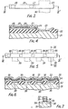
- FIG. 1 and Figure 2 on the upper surface of the n-type semiconductor substrate (1) is provided an insulation layer (2).
- the substrate (1) is of silicon (Si) and the layer (2) is made of silicon oxide (Si0 2 ).
- the insulation layer (2) has a thickness of about seven or eight thousand angstroms (700-800 nm) and is formed by chemical vapour deposition technique, and the polycrystalline silicon layer (3) covers selected portions thereof with a thickness of about three hundred nm.
- the polycrystalline silicon layer (3) is formed to cover the whole surface of the insulation layer (2), and subsequently it is partially etched away by a photo-engraving process.
- the surface of the polycrystalline silicon layer (3) is then oxidized using a thermal oxidation process to form a silicon oxide layer (4).
- the silicon oxide layer (4) has a thickness of about one hundred nm, and has two contact holes (5) and (6).
- the holes (5) and (6) are formed by the photo-engraving process.
- a second polycrystalline silicon layer (7) is formed over the silicon oxide layer (4) with a thickness of about three of four hundred nm and makes contact with the first polycrystalline silicon layer (3) through the contact holes (5) and (6).
- the second polycrystalline silicon layer (7) is formed in substantially the same pattern as the first polycrystalline silicon layer (3) and operates as the main wiring layer.
- An insulation (8) is formed to cover them.
- the insulation layer (8) is made of silicon oxide and has a thickness of 1.3 micron. In this embodiment, the insulation layer (8) is formed by a chemical vapour deposition technique. After the covering process, two contact holes (9) and (10) are formed by photo engraving process.
- aluminium layers (11) and (12) applied over selected portions of the insulator layer (8) make contact with the second polycrystalline silicon layer (7).
- the aluminium layers (11) and (12) are connected through the polycrystalline silicon layers (3) and (7) to circuit elements formed on the substrate. Further, the aluminium layer (13) positioned on the insulator layer (8) crosses over the first and second polycrystalline silicon layers (3) and (7).
- the aluminium layers (11) and (12) and the polycrystalline silicon layers (3) and (7) operate together as wiring layers, their total resistance is low. The resistance of the aluminium is very low, but that of the polycrystalline silicon is higher than the aluminium.
- the polycrystalline silicon layers (3) and (7) are connected in parallel, so that their resistance is about one half of that of one polycrystalline silicon layer alone. Further, as the change in level at the edge of the two polycrystalline silicon layers is made less abrupt by the existence of the silicon oxide layer (4), the aluminium layers (11) and (12) will not be pierced by the edge. In order to further reduce the abruptness of the change of level, the layer 7 can be made slightly smaller so that its edge does not coincide with that of layer 4.
- Figures 3 and 4 show a second embodiment of this invention.
- a thick film silicon oxide layer (22) is formed by using a selective oxidation process.
- the first polycrystalline silicon layer (24) is formed on the selected position of the silicon oxide layer (22).
- This layer (24) operates as the secondary wiring layer for a further polycrystalline silicon layer (25) formed thereover.
- the polycrystalline silicon layers (24) and (25) become conductive by doping with an impurity such as phosphorus, boron or the like.
- the polycrystalline silicon layer (24) is covered by a silicon oxide layer (26).
- the silicon oxide layer (26) has two contact holes (27) and (28) formed by a photo-engraving process and is formed by thermal oxidation of the surface of the polycrystalline silicon layer (24).
- a silicon oxide iayer (23) forming the gate of a MOS FET and having a thickness of one hundred nm, formed at the same time, simplifying the manufacturing process.
- the second polycrystalline silicon layer (25) is then formed over the layer 26 and the exposed portions of layers 22 and 24.
- the polycrystalline silicon layer (25) thus operates as the gate electrode of the MOS FET and as a wiring layer, being connected in parallel with the first polycrystalline silicon layer (24) through the two contact holes (27) and (28) in order to decrease the resistance.
- the source region (29) and the drain region (30) of the MOS FET are formed in the substrate (21) by diffusing phosphorus as an N-type impurity using the gate silicon oxide layer (23) and the polycrystalline silicon layer (25) as a mask.
- FIGS 5 and 6 show the third embodiment of this invention.
- a plurality of MOS FETs are regularly arranged in the semiconductor substrate (31), and constitute a memory array. They are formed in the following way:
- the silicon oxide layer (35), the first polycrystalline silicon layer (34) and the gate silicon oxide layer (33) are etched using the second polycrystalline silicon layer (37) over the channel region of the MOS FETs as the mask so as to leave suitable portions positioned over the channel region of MOS FET to form masks for forming the source and drain regions.
- these layers (33), (34) and (35) will be formed with the same width as the second polycrystalline silicon layer (37).
- an n-type impurity is doped into the p-type substrate (31), and the source regions (38) and the drain regions (39) are formed therein.
- the length between source and drain regions (38) and (39) is equal to the width of the layers (34) and (37), (see Figure 7) so the electric field of the gate electrode (34) and (37) will be uniformly applied to the channel region.
- This method of construction avoids the possibility of the layer (37) being formed out of register with the layer (34), which could cause the length of the channel region to be non-uniform because of the gap between the two layers (34) and (37), so that the electric field of the gate electrodes (34) and (37) would become non-uniform and the characteristics of the MOS FETs would become inferior.
- the channel length of MOS FET is made more uniform and the resistance of the wiring layer and the gate electrode is kept very low, so that the circuit will be able to operate at high speed and the whole device will be of compact construction and have superior electrical characteristics.
- connection between the first and second polycrystalline silicon layers can be accomplished by a greater number of contact holes or they may be laminated directly on one another. Then the connecting resistance may be made smaller, but the positioning of two layers and the whole process will become more critical, because the wiring pattern is generally very complicated.
- the contact holes for connecting the two layers can be formed at the same time that the direct contact holes, connecting the polycrystalline silicon layer and the diffusion layer in the substrate, are formed. Then the process will be simplified. Further, the thermal oxidation process can be substituted by a chemical vapour deposition process, and a predoped polycrystalline silicon layer may be used instead of doping impurity into the polycrystalline layer during the manufacturing process.
Landscapes
- Semiconductor Integrated Circuits (AREA)
- Metal-Oxide And Bipolar Metal-Oxide Semiconductor Integrated Circuits (AREA)
- Semiconductor Memories (AREA)
- Design And Manufacture Of Integrated Circuits (AREA)
- Internal Circuitry In Semiconductor Integrated Circuit Devices (AREA)
Claims (9)
Applications Claiming Priority (2)
| Application Number | Priority Date | Filing Date | Title |
|---|---|---|---|
| JP27361/79 | 1979-03-09 | ||
| JP2736179A JPS55120150A (en) | 1979-03-09 | 1979-03-09 | Semiconductor device |
Publications (2)
| Publication Number | Publication Date |
|---|---|
| EP0016577A1 EP0016577A1 (fr) | 1980-10-01 |
| EP0016577B1 true EP0016577B1 (fr) | 1983-04-13 |
Family
ID=12218902
Family Applications (1)
| Application Number | Title | Priority Date | Filing Date |
|---|---|---|---|
| EP80300661A Expired EP0016577B1 (fr) | 1979-03-09 | 1980-03-05 | Dispositif semiconducteur à circuit intégré comprenant une couche d'interconnexion double |
Country Status (3)
| Country | Link |
|---|---|
| EP (1) | EP0016577B1 (fr) |
| JP (1) | JPS55120150A (fr) |
| DE (1) | DE3062675D1 (fr) |
Cited By (1)
| Publication number | Priority date | Publication date | Assignee | Title |
|---|---|---|---|---|
| DE3635259A1 (de) * | 1985-10-16 | 1987-04-16 | Mitsubishi Electric Corp | Redundante verdrahtung in einer halbleitervorrichtung |
Families Citing this family (24)
| Publication number | Priority date | Publication date | Assignee | Title |
|---|---|---|---|---|
| JPS56161668A (en) * | 1980-05-16 | 1981-12-12 | Hitachi Ltd | Semiconductor device |
| DE3123348A1 (de) * | 1980-06-19 | 1982-03-18 | Tokyo Shibaura Denki K.K., Kawasaki, Kanagawa | Halbleiterbaustein und verfahren zu dessen herstellung |
| JPS5756959A (en) * | 1980-09-22 | 1982-04-05 | Toshiba Corp | Semiconductor device and manufacture thereof |
| JPS5756958A (en) * | 1980-09-22 | 1982-04-05 | Toshiba Corp | Semiconductor device |
| JPS57194552A (en) * | 1981-05-25 | 1982-11-30 | Matsushita Electric Ind Co Ltd | Signal transmission line |
| JPS57211249A (en) * | 1981-06-22 | 1982-12-25 | Nec Corp | Integrated circuit device |
| JPS5834946A (ja) * | 1981-08-27 | 1983-03-01 | Nec Corp | 半導体集積回路装置 |
| JPS5854654A (ja) * | 1981-09-28 | 1983-03-31 | Nec Corp | 半導体集積回路装置 |
| JPS5860561A (ja) * | 1981-10-06 | 1983-04-11 | Mitsubishi Electric Corp | 半導体集積回路装置 |
| JPS5893347A (ja) * | 1981-11-30 | 1983-06-03 | Toshiba Corp | Mos型半導体装置及びその製造方法 |
| JPS58219747A (ja) * | 1982-06-14 | 1983-12-21 | Nec Corp | マスタスライス型半導体装置 |
| JPS594050A (ja) * | 1982-06-30 | 1984-01-10 | Fujitsu Ltd | 半導体装置 |
| JPS5940549A (ja) * | 1982-08-30 | 1984-03-06 | Nippon Telegr & Teleph Corp <Ntt> | 多層配線構造体 |
| JPS5952851A (ja) * | 1982-09-18 | 1984-03-27 | Mitsubishi Electric Corp | 半導体集積回路 |
| JPS60128651A (ja) * | 1983-12-15 | 1985-07-09 | Fujitsu Ltd | 半導体装置 |
| JPS60144238U (ja) * | 1984-03-06 | 1985-09-25 | 富士通株式会社 | 半導体装置 |
| DE3585756D1 (de) * | 1984-07-02 | 1992-05-07 | Fujitsu Ltd | Halbleiterschaltungsanordnung in hauptscheibentechnik. |
| JPH0789568B2 (ja) * | 1986-06-19 | 1995-09-27 | 日本電気株式会社 | 集積回路装置 |
| JPS63268258A (ja) * | 1987-04-24 | 1988-11-04 | Nec Corp | 半導体装置 |
| US5316974A (en) * | 1988-12-19 | 1994-05-31 | Texas Instruments Incorporated | Integrated circuit copper metallization process using a lift-off seed layer and a thick-plated conductor layer |
| JPH02127042U (fr) * | 1990-04-12 | 1990-10-19 | ||
| EP0482556A1 (fr) * | 1990-10-22 | 1992-04-29 | Nec Corporation | Elément de résistance en polysilicium et dispositif à semi-conducteur l'utilisant |
| GB2254487B (en) * | 1991-03-23 | 1995-06-21 | Sony Corp | Full CMOS type static random access memories |
| GB2263018B (en) * | 1991-03-23 | 1995-06-21 | Sony Corp | Static random access memories |
Family Cites Families (1)
| Publication number | Priority date | Publication date | Assignee | Title |
|---|---|---|---|---|
| JPS53124084A (en) * | 1977-04-06 | 1978-10-30 | Hitachi Ltd | Semiconductor memory device containing floating type poly silicon layer and its manufacture |
-
1979
- 1979-03-09 JP JP2736179A patent/JPS55120150A/ja active Pending
-
1980
- 1980-03-05 EP EP80300661A patent/EP0016577B1/fr not_active Expired
- 1980-03-05 DE DE8080300661T patent/DE3062675D1/de not_active Expired
Cited By (1)
| Publication number | Priority date | Publication date | Assignee | Title |
|---|---|---|---|---|
| DE3635259A1 (de) * | 1985-10-16 | 1987-04-16 | Mitsubishi Electric Corp | Redundante verdrahtung in einer halbleitervorrichtung |
Also Published As
| Publication number | Publication date |
|---|---|
| DE3062675D1 (en) | 1983-05-19 |
| EP0016577A1 (fr) | 1980-10-01 |
| JPS55120150A (en) | 1980-09-16 |
Similar Documents
| Publication | Publication Date | Title |
|---|---|---|
| EP0016577B1 (fr) | Dispositif semiconducteur à circuit intégré comprenant une couche d'interconnexion double | |
| US4041518A (en) | MIS semiconductor device and method of manufacturing the same | |
| US4329706A (en) | Doped polysilicon silicide semiconductor integrated circuit interconnections | |
| EP0186855B1 (fr) | Dispositif semi-conducteur de mémoire morte et méthode de fabrication | |
| EP0319215B1 (fr) | Procédé pour fabriquer des circuits intégrés comportant des FETs | |
| US4663644A (en) | Semiconductor device and method of manufacturing the same | |
| GB1567197A (en) | Methods of manufacturing semiconductor devices | |
| EP0070402B1 (fr) | Procédé pour former des configurations électroconductrices sur un dispositif semiconducteur, et un dispositif semiconducteur fabriqué par le procédé | |
| US4353085A (en) | Integrated semiconductor device having insulated gate field effect transistors with a buried insulating film | |
| KR100328332B1 (ko) | 반도체 장치 및 그 제조방법 | |
| EP0193934B1 (fr) | Circuit intégré semi-conducteur et son procédé de fabrication | |
| KR900007048B1 (ko) | 종형 mos 반도체장치 | |
| GB2078443A (en) | Fabricating memory cells in semiconductor integrated circuits | |
| JP2773221B2 (ja) | 半導体装置 | |
| CA1139014A (fr) | Methode de fabrication d'un dispositif dans une plaquette de silicium | |
| EP0034341B1 (fr) | Procédé de fabrication d'un dispositif semiconducteur | |
| US4441941A (en) | Method for manufacturing a semiconductor device employing element isolation using insulating materials | |
| EP0534203B1 (fr) | Dispositif à semi-conducteur | |
| KR940003606B1 (ko) | 반도체장치 | |
| US5280188A (en) | Method of manufacturing a semiconductor integrated circuit device having at least one bipolar transistor and a plurality of MOS transistors | |
| JP2729422B2 (ja) | 半導体装置 | |
| JPH02246264A (ja) | 半導体装置およびその製造方法 | |
| US5714787A (en) | Semiconductor device with a reduced element isolation region | |
| EP0035690B1 (fr) | Dispositif semiconducteur comportant des composants isolés et procédé pour sa fabrication | |
| JPH07130898A (ja) | 半導体装置およびその製造方法 |
Legal Events
| Date | Code | Title | Description |
|---|---|---|---|
| PUAI | Public reference made under article 153(3) epc to a published international application that has entered the european phase |
Free format text: ORIGINAL CODE: 0009012 |
|
| AK | Designated contracting states |
Designated state(s): DE FR GB |
|
| 17P | Request for examination filed |
Effective date: 19810309 |
|
| GRAA | (expected) grant |
Free format text: ORIGINAL CODE: 0009210 |
|
| AK | Designated contracting states |
Designated state(s): DE FR GB |
|
| REF | Corresponds to: |
Ref document number: 3062675 Country of ref document: DE Date of ref document: 19830519 |
|
| ET | Fr: translation filed | ||
| REG | Reference to a national code |
Ref country code: FR Ref legal event code: CD |
|
| REG | Reference to a national code |
Ref country code: GB Ref legal event code: 746 |
|
| PGFP | Annual fee paid to national office [announced via postgrant information from national office to epo] |
Ref country code: FR Payment date: 19950309 Year of fee payment: 16 Ref country code: DE Payment date: 19950309 Year of fee payment: 16 |
|
| PG25 | Lapsed in a contracting state [announced via postgrant information from national office to epo] |
Ref country code: FR Effective date: 19961129 |
|
| PG25 | Lapsed in a contracting state [announced via postgrant information from national office to epo] |
Ref country code: DE Effective date: 19961203 |
|
| REG | Reference to a national code |
Ref country code: FR Ref legal event code: ST |
|
| PGFP | Annual fee paid to national office [announced via postgrant information from national office to epo] |
Ref country code: GB Payment date: 19980224 Year of fee payment: 19 |
|
| PG25 | Lapsed in a contracting state [announced via postgrant information from national office to epo] |
Ref country code: GB Free format text: LAPSE BECAUSE OF NON-PAYMENT OF DUE FEES Effective date: 19990305 |
|
| GBPC | Gb: european patent ceased through non-payment of renewal fee |
Effective date: 19990305 |
|
| PLBE | No opposition filed within time limit |
Free format text: ORIGINAL CODE: 0009261 |
|
| STAA | Information on the status of an ep patent application or granted ep patent |
Free format text: STATUS: NO OPPOSITION FILED WITHIN TIME LIMIT |