EP0019988A1 - Système de sélection des lignes de mot dans une mémoire bipolaire à accès aléatoire - Google Patents
Système de sélection des lignes de mot dans une mémoire bipolaire à accès aléatoire Download PDFInfo
- Publication number
- EP0019988A1 EP0019988A1 EP80300458A EP80300458A EP0019988A1 EP 0019988 A1 EP0019988 A1 EP 0019988A1 EP 80300458 A EP80300458 A EP 80300458A EP 80300458 A EP80300458 A EP 80300458A EP 0019988 A1 EP0019988 A1 EP 0019988A1
- Authority
- EP
- European Patent Office
- Prior art keywords
- voltage
- word lines
- read mode
- current
- potentials
- Prior art date
- Legal status (The legal status is an assumption and is not a legal conclusion. Google has not performed a legal analysis and makes no representation as to the accuracy of the status listed.)
- Granted
Links
Images






Classifications
-
- G—PHYSICS
- G11—INFORMATION STORAGE
- G11C—STATIC STORES
- G11C11/00—Digital stores characterised by the use of particular electric or magnetic storage elements; Storage elements therefor
- G11C11/21—Digital stores characterised by the use of particular electric or magnetic storage elements; Storage elements therefor using electric elements
- G11C11/34—Digital stores characterised by the use of particular electric or magnetic storage elements; Storage elements therefor using electric elements using semiconductor devices
- G11C11/40—Digital stores characterised by the use of particular electric or magnetic storage elements; Storage elements therefor using electric elements using semiconductor devices using transistors
- G11C11/41—Digital stores characterised by the use of particular electric or magnetic storage elements; Storage elements therefor using electric elements using semiconductor devices using transistors forming static cells with positive feedback, i.e. cells not needing refreshing or charge regeneration, e.g. bistable multivibrator or Schmitt trigger
- G11C11/411—Digital stores characterised by the use of particular electric or magnetic storage elements; Storage elements therefor using electric elements using semiconductor devices using transistors forming static cells with positive feedback, i.e. cells not needing refreshing or charge regeneration, e.g. bistable multivibrator or Schmitt trigger using bipolar transistors only
- G11C11/4116—Digital stores characterised by the use of particular electric or magnetic storage elements; Storage elements therefor using electric elements using semiconductor devices using transistors forming static cells with positive feedback, i.e. cells not needing refreshing or charge regeneration, e.g. bistable multivibrator or Schmitt trigger using bipolar transistors only with at least one cell access via separately connected emittors of said transistors or via multiple emittors, e.g. T2L, ECL
-
- G—PHYSICS
- G11—INFORMATION STORAGE
- G11C—STATIC STORES
- G11C11/00—Digital stores characterised by the use of particular electric or magnetic storage elements; Storage elements therefor
- G11C11/21—Digital stores characterised by the use of particular electric or magnetic storage elements; Storage elements therefor using electric elements
- G11C11/34—Digital stores characterised by the use of particular electric or magnetic storage elements; Storage elements therefor using electric elements using semiconductor devices
- G11C11/40—Digital stores characterised by the use of particular electric or magnetic storage elements; Storage elements therefor using electric elements using semiconductor devices using transistors
- G11C11/41—Digital stores characterised by the use of particular electric or magnetic storage elements; Storage elements therefor using electric elements using semiconductor devices using transistors forming static cells with positive feedback, i.e. cells not needing refreshing or charge regeneration, e.g. bistable multivibrator or Schmitt trigger
- G11C11/411—Digital stores characterised by the use of particular electric or magnetic storage elements; Storage elements therefor using electric elements using semiconductor devices using transistors forming static cells with positive feedback, i.e. cells not needing refreshing or charge regeneration, e.g. bistable multivibrator or Schmitt trigger using bipolar transistors only
- G11C11/4113—Digital stores characterised by the use of particular electric or magnetic storage elements; Storage elements therefor using electric elements using semiconductor devices using transistors forming static cells with positive feedback, i.e. cells not needing refreshing or charge regeneration, e.g. bistable multivibrator or Schmitt trigger using bipolar transistors only with at least one cell access to base or collector of at least one of said transistors, e.g. via access diodes, access transistors
-
- G—PHYSICS
- G11—INFORMATION STORAGE
- G11C—STATIC STORES
- G11C11/00—Digital stores characterised by the use of particular electric or magnetic storage elements; Storage elements therefor
- G11C11/21—Digital stores characterised by the use of particular electric or magnetic storage elements; Storage elements therefor using electric elements
- G11C11/34—Digital stores characterised by the use of particular electric or magnetic storage elements; Storage elements therefor using electric elements using semiconductor devices
- G11C11/40—Digital stores characterised by the use of particular electric or magnetic storage elements; Storage elements therefor using electric elements using semiconductor devices using transistors
- G11C11/41—Digital stores characterised by the use of particular electric or magnetic storage elements; Storage elements therefor using electric elements using semiconductor devices using transistors forming static cells with positive feedback, i.e. cells not needing refreshing or charge regeneration, e.g. bistable multivibrator or Schmitt trigger
- G11C11/413—Auxiliary circuits, e.g. for addressing, decoding, driving, writing, sensing, timing or power reduction
- G11C11/414—Auxiliary circuits, e.g. for addressing, decoding, driving, writing, sensing, timing or power reduction for memory cells of the bipolar type
- G11C11/415—Address circuits
Definitions
- the present invention relates generally to a bipolar memory system and, more particularly, to a system for driving a bipolar RAM which is an abbreviation for a Random Access Memory.
- a bipolar RAM comprises a cell array composed of memory cells each of which includes a flip--flop formed by two cross-coupling connected transistors as a fundamental unit.
- Each of the memory-cells is connected to a word line (W), a hold line (H) and a pair of bit lines (B, B) by which the memory cells can be selected.
- W word line
- H hold line
- B, B bit lines
- One prior art system for driving a bipolar RAM is characterised in that the difference in potential between the selected word line and the other non-selected word lines is substantially the same during the read mode and the write mode.
- the above-mentioned difference in potential is set at the margin of the write operation.
- a system for driving a bipolar RAM whose memory cells are selected by changing the potentials of word lines comprising: a first means for changing the potentials of said word lines responsive to the selected state and the non-selected state thereof, the potential of one selected word line of said word lines being higher than those of the other non-selected word lines, and; a second means for changing the potentials of said non-selected word lines responsive to the read mode and the write mode thereof, the potentials of said non-selected word lines being lower during the write mode than during the read mode, whereby the difference in potential between the selected word line and the other non-selected word lines is smaller during the read mode than during the write mode.
- the data written into the memory cells cannot be destroyed during the read mode after the write mode.
- the difference in potential between the selected word line and the other non-selected word lines is set at the margin of the read operation, so that the reading speed of the memory cells becomes high.
- the memory cells C ij which are of a nonsaturating type (Schottkey clamped type) comprise two cross-coupling connected multi-emitter transistors, the transistor elements of which are indicated by Q C1 and Q C2 whose emitters are connected to bit lines, and Q H1 and QH 2 whose emitters are connected to a hold line, two Schottkey barrier diodes SBD 1 and SBD 2 , and two load resistors R 1 and R 2 whereby a flip-flop is formed.
- the memory cell C 00 is located between a word line W D and a hold line H D through which a constant current I H flows and between a pair of bit lines B 0 and B 0 .
- the word line W D is selected by a word driver WD 0 and the bit line pair B 0 and B 0 are selected by a bit driver BD 0 (not shown) so that the memory cell C 00 can be selected.
- the sense amplifier indicated by the reference SA, detects the data stored in the memory cells during the read mode.
- the write amplifier indicated by the reference WA, produces output voltages V D and V D whose values are different when the potential of a write--enable signal WE is low, which means the write mode, and whose values are the same when the potential of the write--enable signal WE is high, which means the read mode.
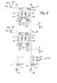
- Fig. 2 which is the main portion of Fig. 1
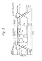
- Fig. 3 which is a timing diagram showing the signals appearing in the circuit of Fig. 2.
- the access operation with regard to the memory cell C 00 (Fig. 1) is shown by the progression of the following steps, as illustrated in Fig. 3.
- the transistor elements Q Hl and Q H2 of the memory cell C 00 which form a flip-flop are conductive and non-conductive, respectively.
- the transistor elements Q C1 and Q C2 of the memory cell C 00 are non-conductive, since the cell C 00 is non-selected.
- the voltages V D and V D of the write amplifier WA(Fig. 1) are the same, which means the read mode.
- the collector potential V BS is represented as follows. where R is the resistance of the resistor R 2 and I B1 is the base current of the transistor element Q Hl . In this case, the value R x I Bl is very small so that the Schottkey barrier diode SBD 2 cuts off.
- V CS the collecter voltage V CS is represented as follows.
- V BE is the forward voltage of the Schottkey barrier diode SBD 1 .
- the collector current I C1 is relatively large so that the Schottkey barrier diode SBD l is conductive.
- the voltage V W0 of the word line W 0 is increased so that the collector voltages V BS and V CS are also increased, while the voltage V W1 of the word line W I is decreased, as illustrated in Fig. 3.
- the voltages V D and V D which are the same, are preset to be between the voltages V BS and V CS .
- the voltages V D and V D equal (V BS + V CS )/2.
- the transistor element Q C1 since the transistor element Q C1 , to whose base is applied the voltage V BS , and a transistor Q 0 , to whose base is applied the voltage V D which is smaller than the voltage V BS form a current switch, the transistor element Q C1 conducts and the transistor Q 0 remains non-conductive. Similarly, since the transistor elements Q C2 and the transistor Q 0 ' form a current switch, the transistor element Q C1 remains non--conductive and the transistor Q 0 ' conducts. As a result, currents indicated by arrows Xl and X2 flow through data bit lines DB and DB, respectively. Therefore, the currents I D and I D supplied to the sense amplifier SA are represented as follows. In this case, the output data D ouT of the sense amplifier SA is, for example, the logic "0".
- the voltage V D is decreased which means the write mode for writing the logic "I".
- the difference in potential between the voltages V CS and V D is, for example, higher than 200 mV.
- the voltages V BS and V CS becomes low and high, respectively, so that the state of the flip-flop is reversed.
- the voltage V D is increased in order to speed up the write operation.
- the voltage V D can remain at the same level as the read mode. In this case, the write speed becomes lower.
- the levels of the voltages V D and V D are the same.
- currents indicated by arrows Yl and Y2 through the data bit lines DB and DB, respectively. Therefore, the currents I D and I D supplied to the sense amplifier SA are represented as follows. In this case, the output data D ouT of the sense amplifier SA is the logic "1".
- the voltage V W0 of the word line W 0 is decreased so that the collector voltages V BS and V CS are slso decreased.
- the decrease of the voltages V BS and V CS takes a longer time than the decrease of the voltage V W0 .
- the voltage V W1 of the word line W 1 is increased.
- both of the voltages V BN and V CN of the memory cell C 01 should always be lower than the voltage V D and V D so that the transistor elements Q C1 and Q C2 thereof are always non--conductive. Therefore, the access operation against the memory cell C 01 is never effected.
- the voltage V D and the voltage V W1 during the write mode in the selected state should satisfy the following inequality.
- the voltages V D and V D should be higher than the voltage of the non-selected word line.
- the transistor element Q H2 of the non-selected memory cell C 01 is conductive, the transistor element Q C2 conducts so that current from the non-selected memory cell C 01 flows through the bit line B 0 .
- the write operation may be not made.
- the difference ⁇ V 1 in potential between the voltages V BS and V CS is about 4 00 or 500 mV and the difference ⁇ V 2 in potential between the voltages V CS and V D is about 200 mV in the non-saturating type memory cells using Schottkey barrier diodes (Fig. 1).
- the difference ⁇ V 1 in potential is about 700 mV in the saturating type memory cells using p-n junction diodes.
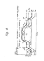
- Fig. 4 is a timing diagram showing signals appearing in the circuit of Fig. 2, by using another driving system of the prior art (Ref. Japanese public Disclosure No. 50-139635).
- the voltage V W0 of the selected word line W 0 is changed higher, as indicated by an arrow A. Therefore, during the read mode, the difference ⁇ W' in potential between the selected word line W 0 and the non-selected word line W 1 is smaller than the difference ⁇ W(Fig. 3) in potential.
- the time which corresponds to ⁇ t' required to charge the selected word line with stray capacity is smaller than the time At (Fig.
- Fig. 5 is a timing diagram showing the signals appearing in the circuit of Fig. 2, by using the driving system according to the present invention.
- Fig. 5 when the state of the selected word line W 0 is changed from the read mode to the write mode, the voltage V W1 of the non-selected word line W 1 is changed to be lower, as indicated by an arrow C. Therefore, in the same manner as in Fig. 4, during the read mode, the difference ⁇ W' in potential between the selected word line W 0 and the non--selected word line W 1 is small, so that the time which corresponds to ⁇ t' required to charge the selected word line with stray capacity is small. Therefore, the reading speed of the operation, as illustrated in Fig. 5, is also high. Further, after the state of the selected memory cell C 00 is changed from the write mode to the read mode, a phenomenon never occurs wherein the voltage V D is lower than the voltage V BS , so that the data stored in the selected memory cell C 00 will not be destroyed.
- Fig. 6 is a block diagram illustrating the memory cell array of another general bipolar RAM whose memory cells are of an IIL (Integrated Injection Logic) type.
- IIL Integrated Injection Logic
- the difference in potential between bit lines B 0 and B 0 is amplified by a differential amplifier formed by two transistors Q S1 and Q S2 , so that the amplified signals are supplied to a sense amplifier SA.
- the write mode of the memory cell array of Fig. 6 one of two transistors Q B0 and Q B1 is conductive and the other is non-conductive. Therefore, the conditions represented by the above-mentioned inequalities (7) and (8) are unnecessary.
- the driving system whose operation is illustrated in Fig. 5, is applied to the memory cell array of Fig. 6.
- Fig. 7 is a circuit diagram illustrating a general decoder/driver circuit.
- the address signals A 0 , A 1 , A 2 and A 3 are applied to address buffers BF 0 , BF 1 , BF 2 and BF 3 , respectively, so that the address buffers produce the signals A 0 , A 1 , A 2 and A 3 and their inverted signals A 0 , A 1 , A 2 and A3 to bus lines L 0 , L 1 , ..., L 7 .
- Each of sixteen word drivers WD 0 , WD 1 , ..., WD 15 have four inputs which are connected to one of the lines L 0 and L 1 , one of the lines L 2 and L 3 , one of the lines L 4 and L 5 , and one of the lines L 6 and L 7 , respectively. Therefore, only one of the word drivers WD 0 , WD 1 , ..., WD 15 is switched on and the others are switched off. In other words, only one of the word lines W 0 , W 1 , ..., W 15 is selected and the other word lines are non-selected.
- Figs. 8A and 8B are two kinds of circuit diagrams of the address buffer BFi of the decoder/driver circuit of Fig. 7.
- two transistors Q 1 and Q 2 form a current switch.
- the transistors Q I and Q 2 are conductive and non-conductive, respectively, so that the base voltages of the transistors Q 3 and Q 4 are low and high, respectively.
- the voltages of signals Ai(OUT) and Ai(OUT) are low and high, respectively.
- the voltages of signals Ai(OUT) and Ai(OUT) are high and low, respectively.
- Fig. 8B two transistors Q 5 and Q 6 form a current switch. Therefore, when the voltage of the address signal Ai(IN) is lower than a reference voltage V R1 , the transistors Q 5 and Q 6 are conductive and non-conductive, respectively, so that current signals Ai(OUT) and Ai(OUT) are in an off-state and on-state, respectively. Contrary to this, when the voltage of the address signal Ai(IN) is higher than the reference voltage V F1 , the current signals Ai(OUT) and Ai(OUT) are in an on-state and off-state, respectively.
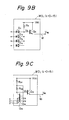
- Figs. 9A, 9B and 9C are three kinds of circuit diagrams of the driver portion of the decoder/driver circuit of Fig. 7.
- transistors Q 7 , Q 8 , Q 9 , Q 10 and Q 11 form a current switch. Therefore, when all the base voltages of the transistors Q 8 , Q 9 , Q10 and Q 11 are lower than a reference voltage V R2 of the transistor Q 7 , all the transistors Q 8 , Q 9 , Q 10 and Q 11 are non-conductive, so that the base voltage V X of a transistor Q X is high ( ⁇ V CC ) and, accordingly, the voltage V Wi of the word line W i is high. This means that the word line W i is selected.
- Fig. 9C a multi-emitter transistor is shown, whose elements are indicated by Q 12 , Q 13 , Q 14 and Q 15 .
- the transistor elements Q 12 , Q 13 , Q 14 and Q 15 correspond to the diodes D 1 , D 2 , D 3 and D 4 , respectively. Therefore, the operation of the word driver of Fig. 9C is similar to that of Fig. 9B.
- the word drivers WD 0 , WD 1 , ..., WD 15 should be those of Fig. 9A.
- the word drivers WD 0 , WD 1 , ..., WD 15 should be those of Fig. 9B or 9C.
- Fig. 10 is a circuit diagram illustrating another general decoder/driver circuit.
- two address signals A 0 and A 1 are converted into four signals A 0 A 1 , A 0 A 1 , A 0 A 1 and A 0 A 1 by address buffers BF O ' and BF 1 '
- two address signals A 2 and A 3 are converted into four signals A 2 A 3 , A 2 A 3 , 2A3 and A 2 A 3 by address buffers BF 2 ' and BF 3 '.
- the expression such as A 0 A 1 is a logical sum between A 0 and A 1 .
- Each of sixteen word drivers WD 0 ', WD 1 ', ..., WD 15 ' have two inputs which receive one of the signals A 0 A 1 , A 0 A 1 , A 0 A 1 and A O A 1 and one of the signals A 2 P 3 , A 2 A 3 , A2A3 and A 2 A 3 , respectively. Therefore, only one of the word drivers WD 0 ', WD 1 ', ..., WD 15 ' is switched on and the others are switched off. In other words, only one of the word lines W 0 , W 1 , ..., W 15 is selected and the other word lines are non-selected.
- Fig. 11 is a circuit diagram of the address buffers BF 0 ' and BF 1 ' of the decoder/driver circuit of Fig. 10.
- two transistors Q 16 and Q 17 form a current switch and two transistors Q 18 and Q 19 form a current switch. Therefore, two address signals A 0 (IN) and A 1 (IN) are converted into the signals A 0 and A 1 and their inverted signals A 0 and A 1 by the current switches.
- the signals A O , A 1 , A 0 and A 1 are supplied to four multi-emitter transistors Q 20 , Q 21 , Q 22 and Q 23 which form four current switches which produce signals A 0 A 1 , A 0 A 1 , A 0 A 1 and A 0 A 1 .
- Fig. 12 is a circuit diagram of the driver portion of the decoder/driver circuit of Fig. 10.
- the circuit of Fig. 12 is the same as that of Fig. 9A, except for the number of inputs. Therefore, the operation of the circuit of Fig. 12 is similar to that of Fig. 9A.
- Fig. 13 is a circuit diagram illustrating a first embodiment of the decoder/driver circuit of the present invention.
- the elements in Fig. 13 which are identical to those of Figs. 7 and 9A are denoted by the same reference numerals as used in Figs. 7 and 9A.
- each of the word drivers WD 0 , WD 1 , ..., WD 15 is the same as that of Fig. 9A, except that the constant current source denoted by Q XS is controlled by a current switching circuit CS1.
- the current switching circuit CS1 which receives a write enable signal WE produces a signal whose voltage is high or low depending upon whether it is for the write mode or the read mode.
- the non-selected word line W 1 at least one of the transistors Q 8 , Q 9 ' Q 10 and Q 11 are conductive so that the current flowing through the resistor RX whose value is also represented by RX is the same as the current I XS flowing the transistor O XS .
- the current I XS in the write mode is larger than that in the read mode and, accordingly, the voltage V x is lower in the write mode than in the read mode. Therefore, the voltage V W1 is lower in the write mode than in the read mode. Contrary to this, in the selected word line W 0 , all the transistors Q 8 .
- the decoder/driver circuit of Fig. 13 can be operated as illustrated in Fig. 5.
- the embodiment of Fig. 13 can be also used in Fig. 10.
- Fig. 14 is a circuit diagram of the current switching circuit CS1 of Fig. 13.
- the voltage of the write enable signal WE is lower than a reference voltage VR3
- the voltage of the signal WE is higher than the reference voltage V R3 . Therefore, in a case of the write mode, a transistor Q21 which forms a current switch with a transistor Q 22 is conductive and the transistor Q 22 is non-conductive. As a result, the base voltage of a transistor Q 23 becomes high and, accordingly, the base voltage of a transistor Q 25 becomes high. As a result, the current I XS is increased.
- the operation of the write mode will be explained in more detail.
- the collector current I C8 of the transistor Q 28 is represented as follows.
- R 12 represents the resistance value of a resistor R 12 as well as the resistor R 12 itself. If the emitter area of a transistor Q 24 is the same as that of the transistor Q 28 , the collector current I C4 of the transistor Q 24 equals I C8 . Therefore, the voltage drop ⁇ V by a resistor R 14 , whose value is also represented by R 14 , is represented as follows.
- the value R 14 determines the constant current I XS in the write mode.
- the transistors Q 21 and Q 22 are non-conductive and conductive, respectively.
- the base voltage of the transistor becomes low which voltage drop is I I R 11 . Since this voltage drop invites the drop of the voltage V 6 whose magnitude is also I 1 ⁇ R 11 , the voltage V 6 is represented as follows.
- the value (V BE - I 1 ⁇ R 11 ) determines the constant current I XS in the read mode.
- Fig. 15 is a circuit diagram illustrating a second embodiment of the decoder/driver circuit of the present invention.
- the elements in Fig. 13 which are identical to those of Figs. 7 and 8B are denoted by the same reference numerals as used in Figs. 7 and 8B.
- each of the address buffers BF O , BF 1 , BF 2 and BF 3 is the same as that of Fig. 8B, except that the constant current source denoted by Q I is controlled by the current switching circuit CS1 of Fig. 14.
- each of the word drivers WD 0 , WD 1 , ... , WD 15 is the same as that of Fig. 9B or 9C.
- the current I X is larger in the write mode than in the read mode.
- the output currents from the address buffers become large which invites the increase of current flowing through the resistor R X (Fig. 9B) or the resistors R X1 and R X2 (Fig. 9C) which belong to the non-selected word driver such as WD 1 .
- the selected word driver such as W 0
- the voltage V X in Fig. 9B or 9C remains high ( ⁇ V CC ) regardless of the write or read mode. Therefore, the decorder/driver circuit of Fig. 15 can be operated as illustrated in Fi g . 5.
- Fig. 16 is a circuit diagram illustrating a third embodiment of the deccder/driver circuit of the present invention.
- each of the address buffers BF 0 , BF 1 , BF 2 and BF 3 comprises two multi-emitter transistors Q 5 ' and Q 6 ', and a transistor Q 7 '.
- each of the word drivers WD 0 , WD 1 , ..., WD 15 is also the same as that of Fig. 9B or 9C.
- the base voltage V RW of the transistor Q 7 ' is controlled by a current switching circuit CS2.
- the current switching circuit CS2 which receives a write enable signal WE produces a signal.
- the voltage V RW of the current switch circuit CS2 is higher than any of the reference voltages V R1 and the voltages of the addresss signals so that the current ⁇ I X flows through the transistor Q 7 '.
- the current flowing through the resistor R X (Fig. 9B) or the resistors R X1 and R X2 (Fi g. 9C) remain I X .
- the voltage V RW is lower than any of the reference voltages V R1 and the voltages of the address signals, so that the current (I X + ⁇ I X ) flows through only one of the transistors Q5' and Q 6 '.
- the current flowing through the resistor R X (Fig. 9B) or the resistors R X1 and R X2 (Fig. 9C) becomes (I X + ⁇ I X ).
- the voltage V X in Fig. 9B or 9C remains high (;V CC ) regardless of the write or read mode.
- the decoder/driver circuit of Fig. 16 can be also operated as illustrated in Fig. 5.
- Fig. 17 is a circuit diagram of the current switching circuit CS2 of Fig. 16.
- the write mode since the voltage of the write enable signal WE is lower than the reference voltage V R3 , transistors Q 31 and Q 32 which form a current switch are conductive and non-conductive, respectively. As a result, the base voltage of a transistor Q 33 becomes low which invites the decrease of the voltage V RW .
- the transistors Q 31 and Q 32 are non-conductive and conductive, respectively. As a result, the base voltage of the transistor Q 33 becomes high, which invites the increase of the voltage V RW . Therefore, the base voltages of the transistors Q 7 ' (Fig. 16) can be controlled by using the current switching circuit of Fig. 17.
- Fig. 18 is a circuit diagram illustrating a fourth embodiment of the decoder/driver circuit of the present invention.
- the elements in Fig. 18 which are identical to those of Figs. 7 and 9A are denoted by the same reference numerals as used in Figs. 7 and 9A.
- each of the word drivers WD 0 , WD 1 , ..., WD 15 is the same as that of Fig. 9A, except that a diode D 13 which is controlled by the current switching circuit CS2 of Fig. 17 is provided.
- the output voltage V RW of the current switching circuit CS2 is applied to the anodes of the diodes D13 , while the cathodes of the diodes D 13 are connected to the bases of the transistors Q X .
- the current switching circuit CS2 produces a signal whose voltage V RW is low in the write mode and high in the read mode. Therefore, the diode D 13 is non-conductive in the write mode and conductive in the read mode.
- the voltage V in the write mode is determined by the voltage drop induced by the resistor R X .
- the voltage V x in the read mode is higher than that in the write mode, since the diode D 13 is conductive.
- the voltage V x is clamped by the diode D 13 .
- the voltage V X is high regardless of the write or read mode.
- the decoder/driver circuit of Fig. 18 can be operated as illustrated in Fig. 5. It should be noted that emitter followers which serve as diodes can be used instead of the diodes D 13 , The embodiment of Fig. 18 can be also used in Fig. 10.
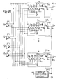
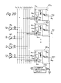
- Figs. 19 and 20 are circuit diagrams illustrating fifth and sixth embodiments of the decoder/driver circuit of the present invention.
- the decoder/driver circuits of Figs. 19 and 20 are similar to that of Fig. 18.
- Each of the word drivers WD 0 , WD 1 , ..., WD 15 of Fig. 19 is based on that of Fig. 9B, while each of them of Fig. 20 is based on that of Fig. 9C.
- the operations of the circuits of Figs. 19 and 20 are the same as that of Fig. 18.
- the number of the word lines is 16.
- the present invention can be also applied to the bipolar memory where the number of word lines are other than 16 such as 32, 64 or 128.
- the system for driving a bipolar RAM according to the present invention has the following advantages, as compared with those of the prior art.
Landscapes
- Engineering & Computer Science (AREA)
- Microelectronics & Electronic Packaging (AREA)
- Computer Hardware Design (AREA)
- Static Random-Access Memory (AREA)
Applications Claiming Priority (2)
| Application Number | Priority Date | Filing Date | Title |
|---|---|---|---|
| JP54023086A JPS5833634B2 (ja) | 1979-02-28 | 1979-02-28 | メモリセルアレイの駆動方式 |
| JP23086/79 | 1979-02-28 |
Publications (2)
| Publication Number | Publication Date |
|---|---|
| EP0019988A1 true EP0019988A1 (fr) | 1980-12-10 |
| EP0019988B1 EP0019988B1 (fr) | 1983-04-13 |
Family
ID=12100607
Family Applications (1)
| Application Number | Title | Priority Date | Filing Date |
|---|---|---|---|
| EP80300458A Expired EP0019988B1 (fr) | 1979-02-28 | 1980-02-18 | Système de sélection des lignes de mot dans une mémoire bipolaire à accès aléatoire |
Country Status (4)
| Country | Link |
|---|---|
| US (1) | US4348747A (fr) |
| EP (1) | EP0019988B1 (fr) |
| JP (1) | JPS5833634B2 (fr) |
| DE (1) | DE3062660D1 (fr) |
Cited By (3)
| Publication number | Priority date | Publication date | Assignee | Title |
|---|---|---|---|---|
| EP0035326A3 (fr) * | 1980-02-08 | 1981-09-23 | Fujitsu Limited | Circuit de décodage |
| EP0037285A3 (en) * | 1980-04-01 | 1983-05-18 | Fujitsu Limited | A memory device, more particularly word line drive circuitry for a memory device |
| EP0485200A1 (fr) * | 1990-11-06 | 1992-05-13 | Nec Corporation | Circuit intégré à semi-conducteur comprenant des portes ECL |
Families Citing this family (14)
| Publication number | Priority date | Publication date | Assignee | Title |
|---|---|---|---|---|
| JPS6010400B2 (ja) * | 1980-10-09 | 1985-03-16 | 富士通株式会社 | 半導体集積回路装置 |
| JPS5841597B2 (ja) * | 1980-12-24 | 1983-09-13 | 富士通株式会社 | 半導体メモリディスチャ−ジ回路 |
| JPH0831278B2 (ja) * | 1981-03-09 | 1996-03-27 | 富士通株式会社 | メモリ回路 |
| DE3227121A1 (de) * | 1982-07-20 | 1984-01-26 | Siemens AG, 1000 Berlin und 8000 München | Schaltungsanordnung zum lesen bipolarer speicherzellen |
| JPS6080195A (ja) * | 1983-10-07 | 1985-05-08 | Fujitsu Ltd | 半導体記憶装置 |
| JPS60254484A (ja) * | 1984-05-31 | 1985-12-16 | Fujitsu Ltd | 2段デコーダ回路 |
| US4613774A (en) * | 1984-07-09 | 1986-09-23 | Advanced Micro Devices, Inc. | Unitary multiplexer-decoder circuit |
| JPS61104394A (ja) * | 1984-10-22 | 1986-05-22 | Mitsubishi Electric Corp | 半導体記憶装置 |
| JPS62202537A (ja) * | 1986-02-19 | 1987-09-07 | Hitachi Ltd | 半導体集積回路装置 |
| JP2793296B2 (ja) * | 1989-11-10 | 1998-09-03 | 株式会社東芝 | 半導体装置 |
| CA2042432A1 (fr) * | 1990-05-31 | 1991-12-01 | Robert M. Reinschmidt | Circuit de selection de memoire |
| US5285118A (en) * | 1992-07-16 | 1994-02-08 | International Business Machines Corporation | Complementary current tree decoder |
| US5276363A (en) * | 1992-08-13 | 1994-01-04 | International Business Machines Corporation | Zero power decoder/driver |
| US6452858B1 (en) * | 1999-11-05 | 2002-09-17 | Hitachi, Ltd. | Semiconductor device |
Citations (9)
| Publication number | Priority date | Publication date | Assignee | Title |
|---|---|---|---|---|
| US3531778A (en) * | 1966-12-22 | 1970-09-29 | Ibm | Data storage devices using cross-coufled plural emitter transistors |
| US3541531A (en) * | 1967-02-07 | 1970-11-17 | Bell Telephone Labor Inc | Semiconductive memory array wherein operating power is supplied via information paths |
| US3636377A (en) * | 1970-07-21 | 1972-01-18 | Semi Conductor Electronic Memo | Bipolar semiconductor random access memory |
| US3703711A (en) * | 1971-01-04 | 1972-11-21 | Honeywell Inf Systems | Memory cell with voltage limiting at transistor control terminals |
| US3713115A (en) * | 1969-05-24 | 1973-01-23 | Honeywell Inf Systems | Memory cell for an associative memory |
| US3736574A (en) * | 1971-12-30 | 1973-05-29 | Ibm | Pseudo-hierarchy memory system |
| NL7710688A (nl) * | 1976-09-29 | 1978-03-31 | Hitachi Ltd | Halfgeleidergeheugen. |
| NL7714013A (nl) * | 1976-12-17 | 1978-06-20 | Hitachi Ltd | Halfgeleidergeheugen. |
| DE2658523A1 (de) * | 1976-12-23 | 1978-06-29 | Siemens Ag | Halbleiterspeicher |
Family Cites Families (3)
| Publication number | Priority date | Publication date | Assignee | Title |
|---|---|---|---|---|
| US3916394A (en) * | 1974-12-09 | 1975-10-28 | Honeywell Inf Systems | High-speed random access memory |
| DE2740565B1 (de) * | 1977-09-08 | 1978-10-19 | Siemens Ag | Schreib-Lese-Ansteueranordnung fuer einen Bipolarhalbleiterspeicher |
| US4172291A (en) * | 1978-08-07 | 1979-10-23 | Fairchild Camera And Instrument Corp. | Preset circuit for information storage devices |
-
1979
- 1979-02-28 JP JP54023086A patent/JPS5833634B2/ja not_active Expired
-
1980
- 1980-02-18 DE DE8080300458T patent/DE3062660D1/de not_active Expired
- 1980-02-18 EP EP80300458A patent/EP0019988B1/fr not_active Expired
- 1980-02-22 US US06/123,643 patent/US4348747A/en not_active Expired - Lifetime
Patent Citations (11)
| Publication number | Priority date | Publication date | Assignee | Title |
|---|---|---|---|---|
| US3531778A (en) * | 1966-12-22 | 1970-09-29 | Ibm | Data storage devices using cross-coufled plural emitter transistors |
| US3541531A (en) * | 1967-02-07 | 1970-11-17 | Bell Telephone Labor Inc | Semiconductive memory array wherein operating power is supplied via information paths |
| US3713115A (en) * | 1969-05-24 | 1973-01-23 | Honeywell Inf Systems | Memory cell for an associative memory |
| US3636377A (en) * | 1970-07-21 | 1972-01-18 | Semi Conductor Electronic Memo | Bipolar semiconductor random access memory |
| US3703711A (en) * | 1971-01-04 | 1972-11-21 | Honeywell Inf Systems | Memory cell with voltage limiting at transistor control terminals |
| US3736574A (en) * | 1971-12-30 | 1973-05-29 | Ibm | Pseudo-hierarchy memory system |
| NL7710688A (nl) * | 1976-09-29 | 1978-03-31 | Hitachi Ltd | Halfgeleidergeheugen. |
| US4156941A (en) * | 1976-09-29 | 1979-05-29 | Hitachi, Ltd. | High speed semiconductor memory |
| NL7714013A (nl) * | 1976-12-17 | 1978-06-20 | Hitachi Ltd | Halfgeleidergeheugen. |
| US4164791A (en) * | 1976-12-17 | 1979-08-14 | Hitachi, Ltd. | Semiconductor memory with equal word line and reference line voltage drop |
| DE2658523A1 (de) * | 1976-12-23 | 1978-06-29 | Siemens Ag | Halbleiterspeicher |
Non-Patent Citations (4)
| Title |
|---|
| IBM TECHNICAL DISCLOSURE BULLETIN Vol. 20, No. 11A, april 1978 Armonk US MARCELLO et al.: "Decode Circuit with Up-Level Clamp", pages 4406-4408 * |
| IEEE JOURNAL OF SOLID-STATE CIRCUITS, Vol. SC13, No. 5, October 1978 New York US HOTTA et al.: "A High Speed Low-Power 40961x1 Bit Bipolar RAM", pages 651-656 * Page 652 and 653, paragraph: "III Cell Margin Increasing Circuitry", figures 1,4,5 * * |
| IEEE JOURNAL OF SOLID-STATE CIRCUITS, Vol. SC13, No. 5, October 1978 New York US KAWARADA et al.: "A Fast 7,5 ns Access 1K-Bit RAM for Cache-Memory Systems", pages 656-663 * Paragraph f "Error-Write Suppression and Bit Line Clamping", pages 659-660; figures 2,4,7,10 * * |
| IEEE JOURNAL OF SOLID-STATE CIRCUITS, Vol. SC2, No. 4, December 1967 New York US IWERSEN et al.: "Beam Lead Sealed-Junction Semi-conductor Memory with Minimal Cell Complexity", pages 196-201. * Page 199, paragraph "Word-Select and Digit Circuits", & US - A - 3 541 531 (BELL) * |
Cited By (3)
| Publication number | Priority date | Publication date | Assignee | Title |
|---|---|---|---|---|
| EP0035326A3 (fr) * | 1980-02-08 | 1981-09-23 | Fujitsu Limited | Circuit de décodage |
| EP0037285A3 (en) * | 1980-04-01 | 1983-05-18 | Fujitsu Limited | A memory device, more particularly word line drive circuitry for a memory device |
| EP0485200A1 (fr) * | 1990-11-06 | 1992-05-13 | Nec Corporation | Circuit intégré à semi-conducteur comprenant des portes ECL |
Also Published As
| Publication number | Publication date |
|---|---|
| JPS55117789A (en) | 1980-09-10 |
| JPS5833634B2 (ja) | 1983-07-21 |
| DE3062660D1 (en) | 1983-05-19 |
| EP0019988B1 (fr) | 1983-04-13 |
| US4348747A (en) | 1982-09-07 |
Similar Documents
| Publication | Publication Date | Title |
|---|---|---|
| EP0019988B1 (fr) | Système de sélection des lignes de mot dans une mémoire bipolaire à accès aléatoire | |
| US4078261A (en) | Sense/write circuits for bipolar random access memory | |
| US4369503A (en) | Decoder circuit | |
| US4322820A (en) | Semiconductor integrated circuit device | |
| US4370736A (en) | Termination circuit for word lines of a semiconductor memory device | |
| US4740917A (en) | Memory using conventional cells to perform a ram or an associative memory function | |
| US4394657A (en) | Decoder circuit | |
| US4198698A (en) | Chip select power-down control circuitry | |
| US4127899A (en) | Self-quenching memory cell | |
| US4460984A (en) | Memory array with switchable upper and lower word lines | |
| US4636990A (en) | Three state select circuit for use in a data processing system or the like | |
| EP0182305A2 (fr) | Mémoire morte | |
| US4625299A (en) | Bipolar random access memory | |
| JPH0217876B2 (fr) | ||
| EP0055409A1 (fr) | Mémoire semi-conductrice | |
| JPS6037555B2 (ja) | メモリ装置 | |
| US4456979A (en) | Static semiconductor memory device | |
| US4821234A (en) | Semiconductor memory device | |
| US4280197A (en) | Multiple access store | |
| EP0181819B1 (fr) | Dispositif d'évacuation d'alimentation d'une cellule de mémoire | |
| US4592023A (en) | Latch for storing a data bit and a store incorporating said latch | |
| US4730275A (en) | Circuit for reducing the row select voltage swing in a memory array | |
| EP0037285B1 (fr) | Dispositif de mémoire, en particulier circuit amplificateur de ligne de mot pour un dispositif de mémoire | |
| EP0023408B1 (fr) | Mémoire à semi-conducteurs comprenant des cellules intégrées à injection logique | |
| US4432076A (en) | Bipolar static semiconductor memory device with a high cell holding margin |
Legal Events
| Date | Code | Title | Description |
|---|---|---|---|
| PUAI | Public reference made under article 153(3) epc to a published international application that has entered the european phase |
Free format text: ORIGINAL CODE: 0009012 |
|
| 17P | Request for examination filed | ||
| AK | Designated contracting states |
Designated state(s): DE GB NL |
|
| GRAA | (expected) grant |
Free format text: ORIGINAL CODE: 0009210 |
|
| AK | Designated contracting states |
Designated state(s): DE GB NL |
|
| REF | Corresponds to: |
Ref document number: 3062660 Country of ref document: DE Date of ref document: 19830519 |
|
| PGFP | Annual fee paid to national office [announced via postgrant information from national office to epo] |
Ref country code: GB Payment date: 19930208 Year of fee payment: 14 |
|
| PGFP | Annual fee paid to national office [announced via postgrant information from national office to epo] |
Ref country code: NL Payment date: 19930228 Year of fee payment: 14 |
|
| PGFP | Annual fee paid to national office [announced via postgrant information from national office to epo] |
Ref country code: DE Payment date: 19930427 Year of fee payment: 14 |
|
| PG25 | Lapsed in a contracting state [announced via postgrant information from national office to epo] |
Ref country code: GB Effective date: 19940218 |
|
| PG25 | Lapsed in a contracting state [announced via postgrant information from national office to epo] |
Ref country code: NL Effective date: 19940901 |
|
| GBPC | Gb: european patent ceased through non-payment of renewal fee |
Effective date: 19940218 |
|
| NLV4 | Nl: lapsed or anulled due to non-payment of the annual fee | ||
| PG25 | Lapsed in a contracting state [announced via postgrant information from national office to epo] |
Ref country code: DE Effective date: 19941101 |
|
| PLBE | No opposition filed within time limit |
Free format text: ORIGINAL CODE: 0009261 |
|
| STAA | Information on the status of an ep patent application or granted ep patent |
Free format text: STATUS: NO OPPOSITION FILED WITHIN TIME LIMIT |