EP0025261A1 - Procédé de fabrication d'un dispositif à semiconducteur - Google Patents
Procédé de fabrication d'un dispositif à semiconducteur Download PDFInfo
- Publication number
- EP0025261A1 EP0025261A1 EP80302337A EP80302337A EP0025261A1 EP 0025261 A1 EP0025261 A1 EP 0025261A1 EP 80302337 A EP80302337 A EP 80302337A EP 80302337 A EP80302337 A EP 80302337A EP 0025261 A1 EP0025261 A1 EP 0025261A1
- Authority
- EP
- European Patent Office
- Prior art keywords
- film
- photoresist
- liquid glass
- glass
- layer
- Prior art date
- Legal status (The legal status is an assumption and is not a legal conclusion. Google has not performed a legal analysis and makes no representation as to the accuracy of the status listed.)
- Granted
Links
Images
Classifications
-
- H—ELECTRICITY
- H10—SEMICONDUCTOR DEVICES; ELECTRIC SOLID-STATE DEVICES NOT OTHERWISE PROVIDED FOR
- H10P—GENERIC PROCESSES OR APPARATUS FOR THE MANUFACTURE OR TREATMENT OF DEVICES COVERED BY CLASS H10
- H10P14/00—Formation of materials, e.g. in the shape of layers or pillars
- H10P14/60—Formation of materials, e.g. in the shape of layers or pillars of insulating materials
- H10P14/63—Formation of materials, e.g. in the shape of layers or pillars of insulating materials characterised by the formation processes
- H10P14/6326—Deposition processes
- H10P14/6342—Liquid deposition, e.g. spin-coating, sol-gel techniques or spray coating
-
- H—ELECTRICITY
- H10—SEMICONDUCTOR DEVICES; ELECTRIC SOLID-STATE DEVICES NOT OTHERWISE PROVIDED FOR
- H10P—GENERIC PROCESSES OR APPARATUS FOR THE MANUFACTURE OR TREATMENT OF DEVICES COVERED BY CLASS H10
- H10P14/00—Formation of materials, e.g. in the shape of layers or pillars
- H10P14/60—Formation of materials, e.g. in the shape of layers or pillars of insulating materials
- H10P14/69—Inorganic materials
- H10P14/692—Inorganic materials composed of oxides, glassy oxides or oxide-based glasses
- H10P14/6921—Inorganic materials composed of oxides, glassy oxides or oxide-based glasses containing silicon
- H10P14/69215—Inorganic materials composed of oxides, glassy oxides or oxide-based glasses containing silicon the material being a silicon oxide, e.g. SiO2
-
- H—ELECTRICITY
- H10—SEMICONDUCTOR DEVICES; ELECTRIC SOLID-STATE DEVICES NOT OTHERWISE PROVIDED FOR
- H10P—GENERIC PROCESSES OR APPARATUS FOR THE MANUFACTURE OR TREATMENT OF DEVICES COVERED BY CLASS H10
- H10P14/00—Formation of materials, e.g. in the shape of layers or pillars
- H10P14/60—Formation of materials, e.g. in the shape of layers or pillars of insulating materials
- H10P14/69—Inorganic materials
- H10P14/692—Inorganic materials composed of oxides, glassy oxides or oxide-based glasses
- H10P14/6921—Inorganic materials composed of oxides, glassy oxides or oxide-based glasses containing silicon
- H10P14/6922—Inorganic materials composed of oxides, glassy oxides or oxide-based glasses containing silicon the material containing Si, O and at least one of H, N, C, F or other non-metal elements, e.g. SiOC, SiOC:H or SiONC
- H10P14/6923—Inorganic materials composed of oxides, glassy oxides or oxide-based glasses containing silicon the material containing Si, O and at least one of H, N, C, F or other non-metal elements, e.g. SiOC, SiOC:H or SiONC the material being boron or phosphorus doped silicon oxides, e.g. BPSG, BSG or PSG
-
- H—ELECTRICITY
- H10—SEMICONDUCTOR DEVICES; ELECTRIC SOLID-STATE DEVICES NOT OTHERWISE PROVIDED FOR
- H10P—GENERIC PROCESSES OR APPARATUS FOR THE MANUFACTURE OR TREATMENT OF DEVICES COVERED BY CLASS H10
- H10P50/00—Etching of wafers, substrates or parts of devices
-
- H—ELECTRICITY
- H10—SEMICONDUCTOR DEVICES; ELECTRIC SOLID-STATE DEVICES NOT OTHERWISE PROVIDED FOR
- H10P—GENERIC PROCESSES OR APPARATUS FOR THE MANUFACTURE OR TREATMENT OF DEVICES COVERED BY CLASS H10
- H10P76/00—Manufacture or treatment of masks on semiconductor bodies, e.g. by lithography or photolithography
- H10P76/20—Manufacture or treatment of masks on semiconductor bodies, e.g. by lithography or photolithography of masks comprising organic materials
- H10P76/202—Manufacture or treatment of masks on semiconductor bodies, e.g. by lithography or photolithography of masks comprising organic materials for lift-off processes
-
- H—ELECTRICITY
- H10—SEMICONDUCTOR DEVICES; ELECTRIC SOLID-STATE DEVICES NOT OTHERWISE PROVIDED FOR
- H10W—GENERIC PACKAGES, INTERCONNECTIONS, CONNECTORS OR OTHER CONSTRUCTIONAL DETAILS OF DEVICES COVERED BY CLASS H10
- H10W20/00—Interconnections in chips, wafers or substrates
- H10W20/01—Manufacture or treatment
- H10W20/031—Manufacture or treatment of conductive parts of the interconnections
- H10W20/056—Manufacture or treatment of conductive parts of the interconnections by filling conductive material into holes, grooves or trenches
- H10W20/058—Manufacture or treatment of conductive parts of the interconnections by filling conductive material into holes, grooves or trenches by depositing on sacrificial masks, e.g. using lift-off
-
- H—ELECTRICITY
- H10—SEMICONDUCTOR DEVICES; ELECTRIC SOLID-STATE DEVICES NOT OTHERWISE PROVIDED FOR
- H10W—GENERIC PACKAGES, INTERCONNECTIONS, CONNECTORS OR OTHER CONSTRUCTIONAL DETAILS OF DEVICES COVERED BY CLASS H10
- H10W20/00—Interconnections in chips, wafers or substrates
- H10W20/01—Manufacture or treatment
- H10W20/071—Manufacture or treatment of dielectric parts thereof
- H10W20/092—Manufacture or treatment of dielectric parts thereof by smoothing the dielectric parts
-
- H—ELECTRICITY
- H10—SEMICONDUCTOR DEVICES; ELECTRIC SOLID-STATE DEVICES NOT OTHERWISE PROVIDED FOR
- H10W—GENERIC PACKAGES, INTERCONNECTIONS, CONNECTORS OR OTHER CONSTRUCTIONAL DETAILS OF DEVICES COVERED BY CLASS H10
- H10W20/00—Interconnections in chips, wafers or substrates
- H10W20/40—Interconnections external to wafers or substrates, e.g. back-end-of-line [BEOL] metallisations or vias connecting to gate electrodes
- H10W20/45—Interconnections external to wafers or substrates, e.g. back-end-of-line [BEOL] metallisations or vias connecting to gate electrodes characterised by their insulating parts
- H10W20/48—Insulating materials thereof
-
- H—ELECTRICITY
- H10—SEMICONDUCTOR DEVICES; ELECTRIC SOLID-STATE DEVICES NOT OTHERWISE PROVIDED FOR
- H10P—GENERIC PROCESSES OR APPARATUS FOR THE MANUFACTURE OR TREATMENT OF DEVICES COVERED BY CLASS H10
- H10P14/00—Formation of materials, e.g. in the shape of layers or pillars
- H10P14/60—Formation of materials, e.g. in the shape of layers or pillars of insulating materials
- H10P14/63—Formation of materials, e.g. in the shape of layers or pillars of insulating materials characterised by the formation processes
- H10P14/6326—Deposition processes
- H10P14/6328—Deposition from the gas or vapour phase
- H10P14/6334—Deposition from the gas or vapour phase using decomposition or reaction of gaseous or vapour phase compounds, i.e. chemical vapour deposition
-
- Y—GENERAL TAGGING OF NEW TECHNOLOGICAL DEVELOPMENTS; GENERAL TAGGING OF CROSS-SECTIONAL TECHNOLOGIES SPANNING OVER SEVERAL SECTIONS OF THE IPC; TECHNICAL SUBJECTS COVERED BY FORMER USPC CROSS-REFERENCE ART COLLECTIONS [XRACs] AND DIGESTS
- Y10—TECHNICAL SUBJECTS COVERED BY FORMER USPC
- Y10S—TECHNICAL SUBJECTS COVERED BY FORMER USPC CROSS-REFERENCE ART COLLECTIONS [XRACs] AND DIGESTS
- Y10S438/00—Semiconductor device manufacturing: process
- Y10S438/942—Masking
- Y10S438/948—Radiation resist
- Y10S438/951—Lift-off
Definitions
- This invention relates to a method of manufacturing a semiconductor device.
- LSI large scale integrated circuits
- VLSI very large scale integrated circuits
- the liquid glass mentioned above is a liquid of which main component is silicic acid made through hydrolysis of methylsilicate which in turn is hardened when treated at high temperature to form an insulator of which main component is silicon dioxide as will be understood from the following: CH 3 0H evaporates when heated and in which h2U also evaporates.
- a film of silicon dioxide obtained by hardening of the liquid glass has a thermal expansion coefficient substantially different from that of a conductive layer of for example aluminium, so that the silicon dioxide film is susceptible to cracking where it is in contact with the conductive layer.
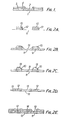
- FIG. 1 of the accompanying drawings is a cross-sectional view of a part of a semiconductor substrate with a conductive layer and an insulator layer formed thereon by a previously proposed method.
- a substrate 1 a conductive layer 2, a film 3 of silicon dioxide formed by hardening a liquid glass, and a PSG layer 4 on the substrate. Cracks are seen at the inter-face of the conductive layer 2 and the film of oxidised silicon 3.
- a liquid such as liquid glass mentioned above generally tends to spread and adhere thinly on upper surfaces of protrusions such as conductive layers and to adhere thickly in indented or depressed regions between conductive layers. In spite of this, great care has been devoted to spreading the liquid thinly so that the glass layer has a thickness in the order of 500 to 2000 A to avoid formation of cracks.
- a method of manufacturing a semiconductor device comprising the step of applying a liquid glass to cover upper surfaces of a layer structure on a semiconductor substrate,characterised by the steps of:-
- the problems referred to above in connection with previous proposals for minimizing differences of level between various layers formed on the surface of a semi- conductor substrate are eliminated by a method in which hardened liquid glass is completely eliminated from the upper surface of a conductive layer, and in which a good thickness of liquid glass is provided in areas between conductive layers.
- a film of photoresist is formed in advance on a region from whencea layer of liquid glass is to be removed, the surface of the film is covered with a liquid glass which is caused to hardened, and then, by removing the film of photoresist, the hardened liquid glass on the film is simultaneously removed by lifting off.
- a semiconductor substrate 11 is . shown with a layer 12 of aluminium conductor of a thickness of approximately 1 Mm patterned thereon.
- a film 10 of photoresist used as a mask for etching at the time of patterning of the conductor layer is left where it is without being removed.
- a liquid glass 13 is applied, by using a conventional spinner for example, and the substrate 11 is then baked at a temperature within the range 170°C to 200°C. So much of the liquid glass is applied that, after said baking, the thickness of a film of hardened liquid glass in an indented or depressed region between conduct 8 r layers 12 is of the order of up to several thousand A.
- the substrate 11 is further baked at high temperatures within the range 450 0 C to 500 0 C.
- the photoresist film 10 is thereby caused to deform and shrinks as illustrated in Fig. 2C, with hardened liquid glass 13 thereon dragged in to expose sides of the photoresist film parts on the conductor layers 12.
- the photoresist film 10 is removed by a solution containing organic solvent for separating the film from the conductor layers 12 . If any resist remains, it will be turned into ashes by oxygen plasma and removed.
- the parts of the hardened liquid glass 13 on the photoresist film 10 formed on the upper surfaces of aluminium conductor layers 12 is also removed simultaneously with the removal of the photoresist film 10 by lift off, and the liquid glass is completely eliminated from the upper surfaces of the conductor layers of aluminium.
- a layer 14 of PSG of a thickness of approximately 1 ⁇ m is formed to cover the formation on the substrate by conventional chemical vapour deposition, and a window is opened for a terminal pad connection as seen in Fig. 2E.
- a film of photoresist may be formed on any surface susceptible to cracking, and liquid glass on the upper surface of the photoresist film may be removed by lift off, allowing a thick film of liquid glass to be formed on the surfaces of parts which have a small expansion coefficient, such as a semi-conductor substrate.
- the method of the invention is valuable for application to integrated circuits of a high packing density, such as LSI devices, and is effective in increasing the reliability of the product.
- a method of manufacturing a semiconductor device embodying this invention comprises the steps of applying liquid glass to cover the upper surfaces of a semi- conductor device and patterning, a film of photoresist is formed in advance on a region from which the layer of liquid glass is to be removed, the liquid glass is applied to cover theupper surface of the film and is caused to be hardened, and thereafter, by removing the photoresist film, the hardened glass on the photoresist is removed simultaneously by lift off.
Landscapes
- Internal Circuitry In Semiconductor Integrated Circuit Devices (AREA)
- Weting (AREA)
Applications Claiming Priority (2)
| Application Number | Priority Date | Filing Date | Title |
|---|---|---|---|
| JP97655/79 | 1979-07-31 | ||
| JP9765579A JPS5621332A (en) | 1979-07-31 | 1979-07-31 | Manufacture of semiconductor device |
Publications (2)
| Publication Number | Publication Date |
|---|---|
| EP0025261A1 true EP0025261A1 (fr) | 1981-03-18 |
| EP0025261B1 EP0025261B1 (fr) | 1983-06-15 |
Family
ID=14198087
Family Applications (1)
| Application Number | Title | Priority Date | Filing Date |
|---|---|---|---|
| EP80302337A Expired EP0025261B1 (fr) | 1979-07-31 | 1980-07-10 | Procédé de fabrication d'un dispositif à semiconducteur |
Country Status (5)
| Country | Link |
|---|---|
| US (1) | US4328263A (fr) |
| EP (1) | EP0025261B1 (fr) |
| JP (1) | JPS5621332A (fr) |
| DE (1) | DE3063768D1 (fr) |
| IE (1) | IE50021B1 (fr) |
Cited By (9)
| Publication number | Priority date | Publication date | Assignee | Title |
|---|---|---|---|---|
| EP0149060A3 (en) * | 1983-11-30 | 1985-07-31 | International Business Machines Corporation | Lift-off process for forming metal patterns |
| EP0134938A3 (en) * | 1983-07-26 | 1985-08-14 | International Business Machines Corporation | Dry process for forming metal patterns on a surface |
| EP0102281A3 (en) * | 1982-08-02 | 1986-03-26 | Fairchild Camera & Instrument Corporation | Adhesion bond-breaking of lift-off regions on semiconductor structures |
| FR2588418A1 (fr) * | 1985-10-03 | 1987-04-10 | Bull Sa | Procede de formation d'un reseau metallique multicouche d'interconnexion des composants d'un circuit integre de haute densite et circuit integre en resultant |
| FR2588417A1 (fr) * | 1985-10-03 | 1987-04-10 | Bull Sa | Procede de formation d'un reseau metallique multicouche d'interconnexion des composants d'un circuit integre de haute densite et circuit integre en resultant |
| EP0263322A3 (en) * | 1986-10-06 | 1988-09-21 | International Business Machines Corporation | Method of making sloped vias |
| EP0443967A1 (fr) * | 1990-02-23 | 1991-08-28 | France Telecom | Procédé de lift-off mécanique d'une couche métallique sur un polymère |
| EP0455413A3 (en) * | 1990-04-30 | 1992-09-16 | American Telephone And Telegraph Company | Method for producing a planar surface in integrated circuit manufacturing |
| US5234539A (en) * | 1990-02-23 | 1993-08-10 | France Telecom (C.N.E.T.) | Mechanical lift-off process of a metal layer on a polymer |
Families Citing this family (5)
| Publication number | Priority date | Publication date | Assignee | Title |
|---|---|---|---|---|
| US4407851A (en) * | 1981-04-13 | 1983-10-04 | Tokyo Shibaura Denki Kabushiki Kaisha | Method for manufacturing semiconductor device |
| US4519872A (en) * | 1984-06-11 | 1985-05-28 | International Business Machines Corporation | Use of depolymerizable polymers in the fabrication of lift-off structure for multilevel metal processes |
| GB8812235D0 (en) * | 1988-05-24 | 1988-06-29 | Jones B L | Manufacturing electronic devices |
| JP3870562B2 (ja) * | 1998-07-16 | 2007-01-17 | セイコーエプソン株式会社 | パターン形成方法、およびパターン形成基板の製造方法 |
| DE10222609B4 (de) * | 2002-04-15 | 2008-07-10 | Schott Ag | Verfahren zur Herstellung strukturierter Schichten auf Substraten und verfahrensgemäß beschichtetes Substrat |
Citations (4)
| Publication number | Priority date | Publication date | Assignee | Title |
|---|---|---|---|---|
| US3723277A (en) * | 1971-07-14 | 1973-03-27 | Molekularelektronik | Method for the production of masks in the manufacture of semiconductor components |
| FR2188304A1 (fr) * | 1972-06-15 | 1974-01-18 | Commissariat Energie Atomique | |
| US4029562A (en) * | 1976-04-29 | 1977-06-14 | Ibm Corporation | Forming feedthrough connections for multi-level interconnections metallurgy systems |
| GB1523677A (en) * | 1975-12-10 | 1978-09-06 | Tokyo Shibaura Electric Co | Semiconductor device and a method for manufacturing the same |
Family Cites Families (3)
| Publication number | Priority date | Publication date | Assignee | Title |
|---|---|---|---|---|
| JPS5394771A (en) * | 1977-01-29 | 1978-08-19 | Fujitsu Ltd | Forming method for thin film pattern |
| JPS53116782A (en) * | 1977-03-22 | 1978-10-12 | Nec Corp | Production of semiconductor device |
| US4181755A (en) * | 1978-11-21 | 1980-01-01 | Rca Corporation | Thin film pattern generation by an inverse self-lifting technique |
-
1979
- 1979-07-31 JP JP9765579A patent/JPS5621332A/ja active Pending
-
1980
- 1980-07-10 EP EP80302337A patent/EP0025261B1/fr not_active Expired
- 1980-07-10 DE DE8080302337T patent/DE3063768D1/de not_active Expired
- 1980-07-11 IE IE1451/80A patent/IE50021B1/en not_active IP Right Cessation
- 1980-07-28 US US06/172,823 patent/US4328263A/en not_active Expired - Lifetime
Patent Citations (4)
| Publication number | Priority date | Publication date | Assignee | Title |
|---|---|---|---|---|
| US3723277A (en) * | 1971-07-14 | 1973-03-27 | Molekularelektronik | Method for the production of masks in the manufacture of semiconductor components |
| FR2188304A1 (fr) * | 1972-06-15 | 1974-01-18 | Commissariat Energie Atomique | |
| GB1523677A (en) * | 1975-12-10 | 1978-09-06 | Tokyo Shibaura Electric Co | Semiconductor device and a method for manufacturing the same |
| US4029562A (en) * | 1976-04-29 | 1977-06-14 | Ibm Corporation | Forming feedthrough connections for multi-level interconnections metallurgy systems |
Cited By (15)
| Publication number | Priority date | Publication date | Assignee | Title |
|---|---|---|---|---|
| EP0102281A3 (en) * | 1982-08-02 | 1986-03-26 | Fairchild Camera & Instrument Corporation | Adhesion bond-breaking of lift-off regions on semiconductor structures |
| EP0134938A3 (en) * | 1983-07-26 | 1985-08-14 | International Business Machines Corporation | Dry process for forming metal patterns on a surface |
| EP0149060A3 (en) * | 1983-11-30 | 1985-07-31 | International Business Machines Corporation | Lift-off process for forming metal patterns |
| EP0223637A1 (fr) * | 1985-10-03 | 1987-05-27 | Bull S.A. | Procédé de formation d'un réseau métallique multicouche d'interconnexion des composants d'un circuit intégré de haute densité |
| FR2588417A1 (fr) * | 1985-10-03 | 1987-04-10 | Bull Sa | Procede de formation d'un reseau metallique multicouche d'interconnexion des composants d'un circuit integre de haute densite et circuit integre en resultant |
| EP0221798A1 (fr) * | 1985-10-03 | 1987-05-13 | Bull S.A. | Procédé de formation d'un réseau métallique d'interconnexion des composants d'un circuit intégré de haute densité |
| FR2588418A1 (fr) * | 1985-10-03 | 1987-04-10 | Bull Sa | Procede de formation d'un reseau metallique multicouche d'interconnexion des composants d'un circuit integre de haute densite et circuit integre en resultant |
| US4826786A (en) * | 1985-10-03 | 1989-05-02 | Bull, S.A. | Method for forming a multilayered metal network for bonding components of a high-density integrated circuit, and integrated circuit produced thereby |
| US4906592A (en) * | 1985-10-03 | 1990-03-06 | Bull S.A. | Method for forming a multilayered metal network for bonding components of a high-density integrated circuit using a spin on glass layer |
| EP0263322A3 (en) * | 1986-10-06 | 1988-09-21 | International Business Machines Corporation | Method of making sloped vias |
| US4830706A (en) * | 1986-10-06 | 1989-05-16 | International Business Machines Corporation | Method of making sloped vias |
| EP0443967A1 (fr) * | 1990-02-23 | 1991-08-28 | France Telecom | Procédé de lift-off mécanique d'une couche métallique sur un polymère |
| FR2658976A1 (fr) * | 1990-02-23 | 1991-08-30 | Schiltz Andre | Procede de lift-off (enlevement d'une couche par decollement d'une couche sous-jacente) mecanique. |
| US5234539A (en) * | 1990-02-23 | 1993-08-10 | France Telecom (C.N.E.T.) | Mechanical lift-off process of a metal layer on a polymer |
| EP0455413A3 (en) * | 1990-04-30 | 1992-09-16 | American Telephone And Telegraph Company | Method for producing a planar surface in integrated circuit manufacturing |
Also Published As
| Publication number | Publication date |
|---|---|
| US4328263A (en) | 1982-05-04 |
| EP0025261B1 (fr) | 1983-06-15 |
| IE801451L (en) | 1981-01-31 |
| JPS5621332A (en) | 1981-02-27 |
| DE3063768D1 (en) | 1983-07-21 |
| IE50021B1 (en) | 1986-02-05 |
Similar Documents
| Publication | Publication Date | Title |
|---|---|---|
| US4770897A (en) | Multilayer interconnection system for multichip high performance semiconductor packaging | |
| EP0025261A1 (fr) | Procédé de fabrication d'un dispositif à semiconducteur | |
| EP0098687B1 (fr) | Procédé pour la formation de dispositifs semi-conducteurs comportant des régions d'isolation diélectrique | |
| US4305974A (en) | Method of manufacturing a semiconductor device | |
| JPH0548617B2 (fr) | ||
| US4292156A (en) | Method of manufacturing semiconductor devices | |
| US4631806A (en) | Method of producing integrated circuit structures | |
| KR100779869B1 (ko) | 전자 부품 및 제조 방법 | |
| EP0263322B1 (fr) | Méthode de fabrication d'ouvertures de contact à bords inclinés | |
| US4321284A (en) | Manufacturing method for semiconductor device | |
| JPH07120650B2 (ja) | スピンオンしたゲルマニウムガラス | |
| KR100253394B1 (ko) | 듀얼 게이트절연막을 가지는 게이트전극의 제조방법 | |
| KR100271941B1 (ko) | 반도체 장치 및 반도체 장치용 절연막 제조 방법 | |
| US4261096A (en) | Process for forming metallic ground grid for integrated circuits | |
| KR960002077B1 (ko) | 반도체 소자 제조방법 | |
| KR100216730B1 (ko) | 반도체 금속막 식각공정 | |
| JPH0427703B2 (fr) | ||
| JPS6321850A (ja) | 半導体装置の製造方法 | |
| KR100206896B1 (ko) | 바이폴라 소자의 컨택형성 방법 | |
| KR0148326B1 (ko) | 반도체 소자의 제조방법 | |
| JPH03185750A (ja) | 半導体装置 | |
| JPS6334956A (ja) | 半導体装置の製造方法 | |
| JPH10326704A (ja) | 薄膜抵抗器の製造方法 | |
| JPS59114838A (ja) | 半導体装置の製造方法 | |
| JPS61216341A (ja) | 半導体装置の製造方法 |
Legal Events
| Date | Code | Title | Description |
|---|---|---|---|
| PUAI | Public reference made under article 153(3) epc to a published international application that has entered the european phase |
Free format text: ORIGINAL CODE: 0009012 |
|
| AK | Designated contracting states |
Designated state(s): DE FR GB NL |
|
| 17P | Request for examination filed |
Effective date: 19810805 |
|
| GRAA | (expected) grant |
Free format text: ORIGINAL CODE: 0009210 |
|
| AK | Designated contracting states |
Designated state(s): DE FR GB NL |
|
| REF | Corresponds to: |
Ref document number: 3063768 Country of ref document: DE Date of ref document: 19830721 |
|
| ET | Fr: translation filed | ||
| PLBE | No opposition filed within time limit |
Free format text: ORIGINAL CODE: 0009261 |
|
| STAA | Information on the status of an ep patent application or granted ep patent |
Free format text: STATUS: NO OPPOSITION FILED WITHIN TIME LIMIT |
|
| 26N | No opposition filed | ||
| PGFP | Annual fee paid to national office [announced via postgrant information from national office to epo] |
Ref country code: GB Payment date: 19940630 Year of fee payment: 15 |
|
| PGFP | Annual fee paid to national office [announced via postgrant information from national office to epo] |
Ref country code: DE Payment date: 19940708 Year of fee payment: 15 |
|
| PGFP | Annual fee paid to national office [announced via postgrant information from national office to epo] |
Ref country code: FR Payment date: 19940711 Year of fee payment: 15 |
|
| PGFP | Annual fee paid to national office [announced via postgrant information from national office to epo] |
Ref country code: NL Payment date: 19940731 Year of fee payment: 15 |
|
| PG25 | Lapsed in a contracting state [announced via postgrant information from national office to epo] |
Ref country code: GB Effective date: 19950710 |
|
| PG25 | Lapsed in a contracting state [announced via postgrant information from national office to epo] |
Ref country code: NL Effective date: 19960201 |
|
| GBPC | Gb: european patent ceased through non-payment of renewal fee |
Effective date: 19950710 |
|
| NLV4 | Nl: lapsed or anulled due to non-payment of the annual fee |
Effective date: 19960201 |
|
| PG25 | Lapsed in a contracting state [announced via postgrant information from national office to epo] |
Ref country code: DE Effective date: 19960402 |
|
| PG25 | Lapsed in a contracting state [announced via postgrant information from national office to epo] |
Ref country code: FR Effective date: 19960430 |
|
| REG | Reference to a national code |
Ref country code: FR Ref legal event code: ST |
|
| REG | Reference to a national code |
Ref country code: FR Ref legal event code: ST |
|
| REG | Reference to a national code |
Ref country code: FR Ref legal event code: ST |