EP0027563A2 - Signalerzeuger für einen Drahtmatrixdrucker - Google Patents
Signalerzeuger für einen Drahtmatrixdrucker Download PDFInfo
- Publication number
- EP0027563A2 EP0027563A2 EP80105786A EP80105786A EP0027563A2 EP 0027563 A2 EP0027563 A2 EP 0027563A2 EP 80105786 A EP80105786 A EP 80105786A EP 80105786 A EP80105786 A EP 80105786A EP 0027563 A2 EP0027563 A2 EP 0027563A2
- Authority
- EP
- European Patent Office
- Prior art keywords
- data
- memory
- block
- stored
- register
- Prior art date
- Legal status (The legal status is an assumption and is not a legal conclusion. Google has not performed a legal analysis and makes no representation as to the accuracy of the status listed.)
- Granted
Links
Images









Classifications
-
- G—PHYSICS
- G06—COMPUTING OR CALCULATING; COUNTING
- G06K—GRAPHICAL DATA READING; PRESENTATION OF DATA; RECORD CARRIERS; HANDLING RECORD CARRIERS
- G06K15/00—Arrangements for producing a permanent visual presentation of the output data, e.g. computer output printers
- G06K15/02—Arrangements for producing a permanent visual presentation of the output data, e.g. computer output printers using printers
- G06K15/10—Arrangements for producing a permanent visual presentation of the output data, e.g. computer output printers using printers by matrix printers
-
- B—PERFORMING OPERATIONS; TRANSPORTING
- B41—PRINTING; LINING MACHINES; TYPEWRITERS; STAMPS
- B41J—TYPEWRITERS; SELECTIVE PRINTING MECHANISMS, i.e. MECHANISMS PRINTING OTHERWISE THAN FROM A FORME; CORRECTION OF TYPOGRAPHICAL ERRORS
- B41J3/00—Typewriters or selective printing or marking mechanisms characterised by the purpose for which they are constructed
- B41J3/01—Typewriters or selective printing or marking mechanisms characterised by the purpose for which they are constructed for special character, e.g. for Chinese characters or barcodes
-
- G—PHYSICS
- G06—COMPUTING OR CALCULATING; COUNTING
- G06K—GRAPHICAL DATA READING; PRESENTATION OF DATA; RECORD CARRIERS; HANDLING RECORD CARRIERS
- G06K2215/00—Arrangements for producing a permanent visual presentation of the output data
- G06K2215/0002—Handling the output data
- G06K2215/0077—Raster outputting to the print element(s)
-
- G—PHYSICS
- G06—COMPUTING OR CALCULATING; COUNTING
- G06K—GRAPHICAL DATA READING; PRESENTATION OF DATA; RECORD CARRIERS; HANDLING RECORD CARRIERS
- G06K2215/00—Arrangements for producing a permanent visual presentation of the output data
- G06K2215/0002—Handling the output data
- G06K2215/0077—Raster outputting to the print element(s)
- G06K2215/008—Raster outputting to the print element(s) from more than one raster memory
Definitions
- Matrix printers and more specifically wire matrix printers are designed to print different types of characters. It is particularly interesting to note that these machines can print characters commonly used in the Far East such as the classic Japanese characters known as Kanji characters. These characters can be printed by a matrix of 18 points on 18 points with two columns of additional points between the characters so that each character requires a horizontal distance of 20 points and a vertical distance of 18 points.
- Conventional wire matrix print heads of the type having a single vertical row of wires can be easily controlled to print the 20-point by 18-point dies required for printing Kanji characters by sending data to each of the the print head when it moves on the paper.
- the present invention relates to a signal generator for a matrix printer for printing characters on a recording medium.
- the printer comprises at least one printhead which moves in front of the recording medium.
- the print head comprises several print elements, each of these print elements being controllable to cause the printing of a symbol.
- the print elements are arranged relative to each other along an oblique axis relative to the path of the print head.
- the signal generator comprises: first means delivering data which represent configurations of symbols constituting characters, each configuration of symbols being included in a character matrix; a memory element from which the data can be stored and from which the stored data can be read; second means for storing in the memory element the symbol configuration data and this, according to an arrangement related to the configuration of the position of the printing elements, and third means for reading the data stored in the element memory column by column or row by row and to control the triggering of the printing elements.
- the particular printer is associated with a main computer system and responds to execution and data signals from the main system to print the paper strip and delivers status signals to the main computer during operation.
- the printer is designed to meet various printing standards for data processing, data gathering, data entry and communication systems. It can be used as a system printer or as a remote station printer.
- the particular printer described here is capable of printing either classic alpha-numeric characters or Katakana alpha-numeric characters (ANK), or more complex characters of the Kanji type.
- the printer is designed so that approximately 3700 different Kanji characters are defined in read-only memory. Due to the tens of thousands of different Kanji characters, there is further provided a read and write memory in which codes defining additional Kanji characters used at the request of customers or newly defined characters such as acronyms, can be stored. This type of character is hereinafter called the Gaiji character.
- the printer is practically similar to printers of this type known in the prior art.
- the print block contains seven print heads of nine wires each instead of eight print heads of eight wires each, and then the paper feed system allows sheets to be fed short distances from to allow printing between previously printed dots.
- Figure 1 shows by way of example a system comprising a main system 1 and the printing system 2 which comprises a printing control unit 3 and the electronic printing circuits 4.
- the execution and data signals are supplied by the main system to the printer control unit 3 by means of the bus bar 5 and the execution and control signals are supplied from the print control unit 3 to the electronic printing circuits 4 by the bus bar 6.
- the status signals are delivered by the print control unit 3 to the main system 1 by means of the bar omnibus 5.
- the main system 1 generates information comprising orders and data and monitors states.
- the printing control unit 3 receives the orders and the data, decodes the orders, searches for the errors and generates status information, controls the printing and the spacing and contains the printing diagnostics.
- the electronic printing circuits 4 execute decoded commands from the control unit, control all the operations carried out by the printer, trigger the printing wires, control the motors, detect the signals emitted by the printing transmitters and control the indicator lights on the operator control panel and switching circuits.
- the electronic circuits 4 also control the tractor / platen elements assembly, the ribbon drive device, the print head carriage, the operator control panel and the print detectors.
- Certain elements of the system include one or more microprocessors or microcomputers for analyzing orders and data and for controlling the various operations to be carried out.
- FIGS 2 and 3 show various elements of the printer which are all housed in the console 10.
- Various access panels or covers such as elements 11, 12 and 13 are provided.
- the upper cover 11 has a window 14 which allows the operator to observe the movement of the paper during the operation of the printer when the cover is closed.
- the recording medium or paper 15 is delivered from a stack 16 and can be driven up or down as seen in Figures 2 and 3 by means of a paper feed assembly 20 which comprises one or more sets of paper traction elements 90 and 91.
- a paper guide 28 guides the paper after printing towards a reception stack (not shown) arranged under the printing device and at the rear of the printer console.
- Printer comprises a printing assembly 30 which is generally arranged in a horizontal plane relative to the paper 1 5 and which is located at the printing station 32.
- the printer ribbon drive assembly 40 is disposed at the front of the printer.
- the print control unit 3 and its associated microprocessors are generally arranged behind the side cover 13.
- a ribbon 41 is wound on one of the reels 42 or 43 which are disposable.
- Each ribbon box will preferably contain a disposable ribbon protective element 46 which is mounted on flexible fasteners 130 and 131 between the printing assembly 30 and the paper 15 to maintain the ribbon 41 in proper alignment and to reduce minimum ink stains on the paper 15.
- the ribbon moves on a path established at the front of the print head around the balusters 125, 126, 127 and 128.
- Two motors drive the ribbon 41 in both directions via the reels 42 and 43.
- the print control unit 3 detects the jams of the ribbon and the end of the ribbon ⁇ (EOR). Ribbon jamming causes an error light to illuminate and stops printing. An EOR condition causes the reversal of the ribbon drive direction.
- the printer comprises an operator control panel 26 composed of several control keys, two indicator lights, an on / off power switch, a display unit, and a control unit. density display.
- a sixteen-position mode switch 65 is disposed behind the front door 12.
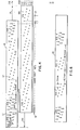
- Figure 4 shows a printing block 50 which comprises seven groups of nine printing wires 52 and the associated control devices (not shown).
- the printing unit 50, the printing wires 52 and the printing control devices are known in the prior art.
- Each group of nine print wires 52 is considered a print head and the print heads are respectively referenced from 1 to 7.
- the printing wires 52 are respectively numbered from left to right and from top to bottom 1 to 9, the wires 1 to 5 being arranged on a first oblique line so that the adjacent wires 52 are separated horizontally by a distance of 10 mm and vertically by a distance of 0.42 mm.
- the wires 6 to 9 are arranged on a second oblique line directly below the wires 1 to 5 and are aligned vertically halfway between the wires 1 to 5.
- the printing block 50 is designed to be driven from the position shown in the upper part of Figure 4, to the right, as indicated by the arrow 54. In normal operation, the printing unit 50 moves to a position shown in the lower part of Figure 4 and referenced 54A. It is obvious that there is only one printing block 50 in the printer 2 and FIG. 4 represents the two extreme positions of a printing block 50. Normally, the print head 50 moves to the right by 5 cm, which is the distance between the print wires 1 and the adjacent print heads. This is sufficient for printing 124 ANK type characters or 62 Kanji characters.
- a detector-transmitter (not shown) coupled to the print head, passes over the transmitter of print signals 56 which delivers an electrical pulse. each time the print head travels 0.254 mm.
- the control circuit of FIGS. 7 and 8 responds to the pulses emitted by the print transmitter by causing the desired print control devices to be excited in order to trigger the print wires 52, which causes the printing of dots on the sheet 15.
- the characters 58 printed on the sheets 15 are shown aligned with the two positions 50 and 50A of the printing block 50 and consist of 62 Kanji words with a width of 20 points each, this line being able to be carried to 66 words if the printing unit 50 moves as indicated by the arrow 54B or be made up of 124 characters ANK or be increased to 132 characters ANK if the printing unit 50 is moved as indicated by the arrow 54B.
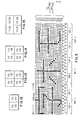
- Figure 5 is a detailed representation of three Kanji words.
- Each of the words is inserted into a dot matrix with a width of 20 columns and a height of 18 rows.
- a point can be printed in any of the 360 positions of each matrix.
- columns 19 and 20 of each matrix are intentionally left blank to allow spacing between adjacent words.
- Each word can be further broken down into two characters of 10 columns each.
- the rows of each matrix are alternately printed during the movement from left to right and from movement from right to left of the printing block 50. Thus, the odd rows can be printed during the movement from left to right of the printing block printing 50 and the even rows can be printed during the movement from right to left of the printing block 50.
- row 1 is printed by the wire 1 while the printing block 50 is driven in the position shown by arrow 54 and row 2 is printed by wire 1 when the printing unit 50 is driven in the direction indicated by arrow 54A.
- row 2 is printed by wire 1 when the printing unit 50 is driven in the direction indicated by arrow 54A.
- the expression “first passage” indicates the movement from left to right of the printing block 50 as indicated by the arrow 54 and the expression “second passage” indicates the movement from the right to the left of the printing block 50 as indicated by the arrow 54A .
- the wire 5 of the print head 1 is aligned with the column 1 of the word 1.
- the wire 1 of head 2 is aligned with column 1 of word 3
- wire 6 of head 2 is aligned with column 1 of word 4.
- Wire 2 of head 2 is aligned with column 1 of word 5 and so . continuation so that the wire 5 of the head 7 is aligned with the column 1 of the word 61.
- the actual movement of the printing block 50 will be prolonged in order to slow it down, stop it, and accelerate its speed so that at when the printing unit 50 moves from right to left as indicated by the arrow 54A, it has reached its full speed by the time when it is ready to ensure printing at the last column of word 2.
- certain dots are printed by a print head and the remaining dots by an adjacent print head.
- the thread 1 of the head 2 prints the points of the first row while the threads 2 to 9 of the head 1 bring the points of the other rows.
- Figure 6 shows a print block 60 which is similar to the print block 50 except that only four heads, each made up of nine wires, are shown.
- the distance separating the wires 1 from the adjacent heads is 88.9 mm instead of 50 mm as in the case of the printing block 50.
- the edge-to-edge movement of the printing block 60 is extended due to the greater distance between adjacent print heads.
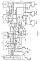
- FIG. 7 shows the control circuit 62.
- the operation of such a circuit will be explained using complex characters (such as Kanji characters), but this circuit, as well as the present invention, can be used for the printing of 'any character.
- the heart of the control circuit 62 is constituted by the communication microprocessor (CMA) 64 and the control microprocessor (CTA) 66.
- the communication microprocessor 64 and the control microprocessor 66 can be microprocessors of the type described in the patent FR -A 2 413 715 filed in France by the plaintiff on December 5, 1978.
- the function of the communication microprocessor 64 is to take data from the main system 1, to apply them via the interface command 68, and converting them to an acceptable wire image which is stored in the wire image memory 70.
- the data applied from the main system 1 includes status, control and character definition information. Only the information concerning the definition of the characters will be treated here.
- Character or data definition information applied from the system main 1 via the command interface 68 are in the form of address codes which define a particular Kanji character stored in the memory 72.
- the memory 72 is composed both of an unalterable memory and a read and write memory. Approximately 3,700 different images of Kanji characters are stored in the immutable part of memory 72 and are arranged in blocks defined by a 16-bit address code.
- the main processor 1 applies a 16-bit code via the interface command 68 to the microprocessor 64.
- the microprocessor 64 then addresses the memory 72 with this code to read the appropriate Kanji character defined by the 16 bits.
- the read / write part of memory 72 contains both Katakana (ANK) and Gaiji alpha-numeric characters.
- the ANK characters are known. These characters have a width of nine columns and a height of seven columns and are printed during a single pass of the printing block 50 moving in one of the directions indicated by the arrows 54 or 54A. When printing ANK characters, thread 1 is not used and thread 9 is used for underlines.
- the Gaiji characters are characters similar to the Kanji characters but not included in the 3700 characters which are stored in the immutable part of the memory 72.
- the code of the images of wires stored in the memory 72 for both the ANK characters and the characters Gaiji is applied from the main system 1 under the control of microprocessor 64 in a known manner. Since the ANK type characters only require half the number of columns, they can be addressed by an eight bit address signal applied from the main system 1. On the other hand, the Gaiji characters which are of the same size as Kanji characters as seen in Figure 5, require a 16 bit address signal.
- the data is delivered from the main system 1 via the interface command 68 and emma stored in the interface memory 74.
- the communication microprocessor 64 verifies the information contained in the interface memory 74 and which may include status commands, execution commands such as feeding the paper or other commands similar or character definition information.
- the character definition information is delivered from the interface memory 74 by the communication microprocessor 64 and stored in the CMA memory 76.
- the CMA memory 76 is composed of both an unalterable memory and a memory read / write.
- the unalterable memory may for example be composed of all of the control microprocessor 64 control instructions and the read / write memory may include an erasable block memory or working memory, as well as an intermediate text memory and a intermediate selection memory.
- the intermediate text memory of the CMA memory 76 is a block of memory used for storing the address codes of the characters to be printed.
- the intermediate text memory is divided into 132 bytes and can be used to define up to 132 ANK characters or 66 Kanji or Gaiji characters.
- the CMA memory 76 includes a second memory block called the intermediate selection memory.
- the intermediate selection memory includes 132 bit positions. A "1" is placed in each position in which a Kanji character, or a Gaiji character is to be printed, and a "0" bit is placed in the bit position of an ANK character.
- the communication microprocessor 64 responds to information delivered to its input STG from the memory CMA 76 via the memory bus STG. In addition, microprocessor 64 responds to information from the data input bus (DBI). The microprocessor 64 delivers data information on the data output bus (DBO) and address information for the input / output devices on the address output bus (ABO) and address information for storage devices on the memory address bus (SAR).
- the CMA 76 memory responds to the signals carried by the memory address buses, the data output buses and the address buses, supplied to the SAR, DI (Data input) and ABO inputs, respectively, and delivers signals instruction via the DO output (Data output) to the memory bus.
- the address information appears on the ABO bus and applied to the memory 76 can be used to control the paging of the memory of the unit 76 and the information appears on the SAR bus defines a specific position in a particular paged memory section. .
- Data applied to the data input (DI) of memory 76 from the data output bus is used to write information to the erasable block memory.
- the data output (DO) of the memory 76 is used to transfer the information read to the memory in the unit 76.
- the control logic 78 and the data register 80 are associated with the assembly 72 composed of a memory unalterable and a memory for reading and writing.
- the control logic 78 responds to signals carried by the address bus and delivered from the communication microprocessor 64 and delivers appropriate signals to address the desired part of the memory 72.
- control logic 78 delivers a signal to block data transmitted to the data register 80 from the memory 72.
- the data register 80 responds to the data delivered from the microprocessor 64 by the data output bus and transmits the data stored in the data register 80 to the microprocessor 64 via the data entry bus. Additionally, data can be transferred to and from memory 72 from and to the data register 80.
- the wire picture memory 70 is an 8-bit 4K byte memory, which, under the control of selection logic 82, selection logic 84 and control logic 86, operates as a double unit 2K 8-bit bytes read and write storage.
- the selection logic 82 responds to address signals applied to the memory address bus from the communication microprocessor 64 and to address signals applied to the memory address bus from the image generator In addition, the selection logic 82 responds to a control signal from the control logic 86 which determines which of the two sets of address signals applied to the selection logic 82 should be applied to address the one of the two parts of the son image memory 70.
- the data output (DO) of the wire image memory 70 is supplied to the selection circuit 84 which also responds to signals transmitted by a selection bus (SEL) from the head image generator 88 and delivers data to the head image generator 88.
- the control logic 86 responds to the data signals carried by the data output bus and to the address signals carried by the address bus and delivered by the communication microprocessor 64 .
- the control microprocessor 66 outputs data signals over the data output bus (DBO) and delivers address signals over the address bus (ABO) and the memory address bus (SAR). In addition, the control microprocessor 66 receives on the one hand instruction signals from the CTA memory 98 by the memory bus (STG) and, on the other hand data by the data bus (DBI).
- the print detection circuit 92 and the print control logic 94 are associated with decoding logic 100 which, in response to signals applied to it by the address bus, determines whether the control logic d 94 must respond to the data applied to the data output bus at its DI input, or select the print detection unit 92 to deliver data from its data output (DO) by the input bus of data to the microprocessor 66.
- the decoding logic 100 selects the print control logic 94 or the detection circuit 92 by decoding the address signal applied to it and by delivering an appropriate signal to the conditioning input of the print control logic 92 or print detection circuit 94.
- the head locking circuit 96 is also associated with the decoding logic 102. This circuit decodes the address signals carried by the address bus and delivers a signal to the conditioning input of the head locking circuit 96 so that it can receive data at its input DI delivered by the data output bus of the microprocessor 66 or can deliver data by its DO output to microprocessor 66 by the data input bus.
- the communication microprocessor 64 and the control microprocessor 66 can exchange information via the command register 104 and the state register 106.
- the decoding logic 108 controls the register 104 and the state register 106 to synchronize the data flowing from the communication microprocessor 64 to the control microprocessor 66, the latter operating normally in an asynchronous manner.
- the input / output element 110 can also be used as a local memory for storing intermediate data during the transfer of data from the communication microprocessor 64 to the control microprocessor 66.
- the command register 104 receives data from the output bus of data from microprocessor 64 and delivers data to the data input bus of microprocessor 66.
- the last block of the electronic control circuit 62 is constituted by the operator control panel 112 which responds to the signals carried by the data output bus and the address bus of the communication microprocessor 64 and delivers signals to the bus of the communication microprocessor 64.
- the table 1.12 operator control communicates with LED display units, restore circuits and switches mounted on the operator control panel 26 shown in Figure 2.
- Figure 8 is a more detailed schematic representation of the wire image memory 70, selection circuits 82 and 84, control circuit 86 and head image generator 88.
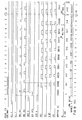
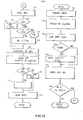
- Figure 9 shows a series of signals used to explain the operation of the assembly of FIG. 8. The description of FIG. 8 will be made in association with FIGS. 10 to 13 which represent the progress of a part of the control program of the communication microprocessor 64 to load the son image in son image memory 70.
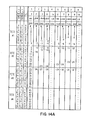
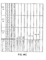
- the organization of son image memory 70 is shown in Figures 14A to 14D, when assembled according to Figure 14, for the printing block with seven heads, and in Figures 15A to 15D assembled according to Figure 15, for the four-head printing block 60. The remaining part of Figure 8 will be described later in relation to the reading of the wire image memory 70 by the image generator head 88.
- the control circuit 86 and the selection circuit 82 perform this function.
- the control circuit 86 is composed of the decoding logic 114 which responds to the address bus from the communication microprocessor 64. For a certain address defining an input / output device such as the control circuit 86, the logic of decoding 114 decodes the address signal from the communication microprocessor 64 and delivers a signal conditioning the AND gate 116. Each time that the communication microprocessor 64 executes an output instruction, the output signal of the CMA microprocessor is delivered, which causes data to pass through the AND gate 116 on a line of the communication microprocessor 64 in flip-flop 118.
- the control of the selection circuits 120 and 122 is also influenced by the control logic 124 which responds to the power selection (SEL P) and high level address selection (AHS) signals from the communication microprocessor 64 and to a signal called "H SAR 11" applied from the H SAR counter 126A which will be described later.
- the control logic 124 delivers the signals H SEL 1 and H SEL 2 to the selection circuits 120 and 122.
- the signals CMA SEL 1 and CMA SEL 2 are applied to the selection circuits 120 and 122 from the communication microprocessor 64. These last two signals are delivered at each cycle of microprocessor 64 in the same way as the signal CMA SEL P.
- the outputs of the selection circuits 120 and 122 are supplied to the four selection inputs of the wire image memory 70 in order to select two of the four rows of elements of the 1K read and write memory of eight bits bytes.
- the address signals of the selected rows of the memory are delivered by the selection circuit 2: 1 128A in response to a memory address signal which is delivered by the communication microprocessor 64 (CMA SAR) or by the counter H SAR 126A.
- CMA SAR communication microprocessor 64
- H SAR When writing to the wire image memory 70, the CMA SAR signal is delivered to address a particular memory byte in which data delivered from the communication microprocessor 64 by the data output bus is written .
- the H SAR signal is delivered to address the byte from which the data is read.
- Figures 10 to 13 and Figures 14A to 14D assembled in the form of Figure 14 show the manner in which 2K selected bytes from the wire image memory 70 are stored.
- the organization of the 2K selected bytes from the son image memory 70 consists of 25 columns of 72 bytes. Each byte is addressed by a hexadecimal number from "000" to "708". Due to the oblique configuration of each printhead, it was determined that the data should be placed in the selected 2K bytes of the wire image memory 70 obliquely, and then read the information by the intermediate of the head image generator 88 column of bits by column of bits. With this arrangement, a considerable saving of material is obtained compared to the techniques used previously.
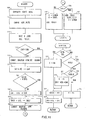
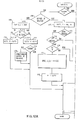
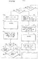
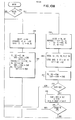
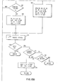
- FIGS. 10 to 13 show the progress of the program of the communication microprocessor 64 and more particularly of the part which allows the loading of the image of the wires into the image memory of wires 70.
- the communication microprocessor 64 begins the execution of the image program of the wires or WI allowing the loading of the appropriate image of wires in the wire image memory 70 at block 129 where the image image memory selected wire 70 is deleted and a configuration of. test is loaded into the portion of thread image memory 70 above the hexadecimal address "708". The test configuration is used to verify operation. Then at block 132, we determine if the printing block 50 contains seven heads. In this case, block 134 indicates that the address of the parameters of the machine with seven heads is set up. If at block 132 it has been determined that the machine is not a seven head machine, it is determined at block 136 that the machine is a four head machine. If the answer is negative, an error state j exists as indicated by block 138.
- Block 140 If it has been determined that it was a four-head machine, the address of the parameters of the four-machine heads is then put in place as indicated in block 140.
- Blocks 134 and 140 meet at the block . 142, which indicates that the parameters selected for the particular number of heads are stored in internal registers of the communication microprocessor 64 and in the erasable element part of the memory CMA 76.
- the parameters include constants concerning the length of each column , an indicator of the intermediate attribute memory, an indicator of the intermediate text memory and various other correction factors and flags that will appear as the program progresses.
- a first pass consists of a movement from left to right of the printing block 50 as indicated by the arrow 54 and is indicated by the command data sent by the main system 1. If it is a first pass, block 148 then indicates that the second pass flag is cleared. If it is not a first pass, block 150 indicates that the flag of the second pass is conditioned. In all cases, block 152 indicates that the word counter is advanced by 1, then the program continues with the WPUTWI part, which is represented by the right column of FIG. 10.
- block 154 indicates that the word counter is counted down. Every sixteen countdowns of the word counter, a connection causes the execution of the interface program in order to determine whether the main processor 1 delivers signals to the interface control 68 or requires them. Then, block 156 indicates that the old selection bit is shifted to the position of the least significant bit (bit 0) of the internal register TAILF and the present selection bit found in the stored selection byte is transferred to the position of the bit 0 of the ATFLG register. The old selection bit was previously in the position of bit 0 of the ATFLG register. Then, according to block 158, the selection counter is increased. The selection counter is made up of bit positions 1, 2 and 3 of the ATFLG register.
- each of the internal registers of microprocessor 64 is a 4-bit register and after the three most significant bits of the ATFLG register have been advanced eight times, the carry flag is conditioned, thus indicating that all the bits of selection contained in the multiplet stored from the selection counter, have been processed. So, in block 160, we determine if the postponement is conditioned. In this case, the next selection byte from the intermediate selection memory is stored. Otherwise, block 162 is skipped.
- an address byte is stored from the position of the intermediate text memory defined by the intermediate text memory indicator and the intermediate text memory indicator is increased. It will be recalled that the organization of the intermediate text memory is such that for Kanji characters, two address bytes or sixteen bits define the address of the particular Kanji character while for ANK characters, only one byte is necessary to define the address of the ANK character.
- the son image is stored in the son image memory 70 for the desired ANK program.
- the WKANWI program is executed if it has been determined in block 166 of Figure 10 that a Kanji character must be stored in the son image memory 70.
- the word counter is counted down and every sixteen countdowns, a connection appears making it possible to manipulate the interface.
- the second byte of the address code of the word Kanji or Gaiji, as the case may be, found in the intermediate text memory is stored in the internal registers of the microprocessor 64.
- the data found in CMA 76 at the address stored following the execution of blocks 134 or 140 are accessed and the TAILF register is updated with this data.
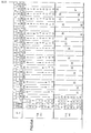
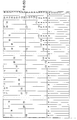
- Figures 14A to 14D show the organization of the wire image memory 70.
- the image of the wires is stored to resemble a matrix of 25 columns in 72 rows, each column containing a byte per row.
- the row called "bytes" indicates each of the 25 columns. Since each Kanji or Gaiji word consists of 20 columns of dots and each byte is made up of eight bits, the 25 bytes or columns define 20 words which are indicated by the top row shown in Figures 14A and 14B.
- each word composed of Kanji or Gaiji characters is divided into two characters of ten bits each.
- each character represents an ANK character and will be treated in a similar manner to that described here with reference to Figures 10 to 13.
- the numbers written in the matrix of Figures 14A to 14D represent characters rather than words.
- the characters 1 and 2 define the word 1
- the characters 3 and 4 define the word 2
- the characters 5 and 6 define the word 3 and so on until characters 131 and 132 which define the word 66. Since each character is 10 columns wide, it is necessary to have more a byte position to define a character.
- the heading under the "Multiplets" row indicates the bytes defined in this particular column in relation to a character. For example, in the first column, the eight high-level bits of a particular character are defined.
- the two low level bits of this character are defined and the six high level bits of the next character are defined.
- the four low-level bits of the second character and the four high-level bits of the third character are defined and in column 4, the six low-level bits of the third character and the two high-level bits of the fourth character are defined.
- the eight low-level bits of the fourth character are defined.
- each row of the matrix defines a wire and, thus, nine rows define a different head.
- heads 1 to 7 are defined by the first sixty-three rows.
- the rows 64 to 72 define the operation of the head 7 in the extended region.
- the column "Wire" indicates the wire to which the particular row of this head refers.
- the first row refers to wire 1, the second row to wire 6, the third row to wire 2 and so on. Note that these wires are in the order in which they appear from left to right.
- the two columns "SLICE (1)” and "SLICE (2)” contain the number of the slice of memory 72 which contains the definition of the Kanji or Gaiji characters.
- the characters are defined by a slice beginning with the first row shown in Figure 5 in the form of slice 1, the second row in the form of slice 2, the third row in the form of slice 3 and so continued to the last row which is represented by slot 18.
- Each slot contains eighteen bits which can be stored in an appropriate manner in a memory comprising two bytes plus two parity bits.
- the memory layout will define the slice for the full eighteen-bit word Gaiji or Kanji of eighteen bits at a single address. Note that each Kanji or Gaiji character requires a maximum of eighteen columns of information to be printed with at least two columns to separate each word. Although it is unnecessary for the memory 72 to contain information relating to the last two separation columns, it is necessary for this information to be placed in the wire image memory 70.
- Block 174 it is determined whether the DAR register has reached "0" when the update data has been subtracted. If yes, it means that it indicated a location to the left of column 1 and that it must be corrected to indicate a different position.
- Block 176 indicates that the flag of the last column is then conditioned and block 178 indicates that the constant UFC is then added to the register DAR. In the case of Figures 14A to 14D, the constant UFC is "6FF" and in the case of Figures 15A to 15D, the constant UFC is "7B3".
- blocks 176, 178, 180, 182 and 184 are then skipped. In all cases, continuing to block 186, the flag of the first tranche is conditioned. Then, in block 188, it is determined whether or not a Kanji character is being printed. This can be done by checking the four most significant bits of the address read from the intermediate text memory. If these four bits are 4 or 5, a Kanji character is being printed. Otherwise it is a Gaiji character. If it is determined that it is a Kanji character, block 190 indicates that the registers SLNUM and SOVFL are deleted and the first byte of the Kanji address obtained from the intermediate text memory is sent to the logic. 78 and locked in a slice indicator register.
- a "1" is added to the SLP3 register where the second pass takes place.
- the registers SLPO, SLP1 and SLP2 contain the address to. twelve bits which gives access to a block of memory which contains the eighteen slices defining a Kanji character.
- the SLP3 register is used as an indicator of the particular tranche involved. In the particular embodiment described here, there are actually two blocks of memory that define a Kanji character.
- the first fifteen sections 1 to 15 are defined in one block and the last three sections or sections 16, 17 and 18 are defined in a second block.
- the two most significant bits of the SLP register 1 are set to 0 at output and transferred to the two most significant bits of the SLP register 3 to define this second block.
- the two least significant bits of the SLP register 3 are then increased to define the particular slice of the second block which is concerned.
- block 192 indicates that the Gaiji address is stored in the slice indicator registers SLPO, SLP1, SLP2 and SLP3. A "1" is stored in the SLNUM register and the SLP3 register is adjusted for the second pass by the addition of a "1". Finally, the memory 72 is conditioned to allow the Gaiji information to be read in its reading and writing part. Whether block 190 or block 192 is executed, operation continues with the WKLOOP 1 program shown in Figure 12.
- Figure 12 shows the WKLOOP1 program. This program is used to lock an information section from memory 72 in the data register 80 and to condition the section indicators SLPO, 1, 2 and 3 for the next section.
- a slice of data is read from memory 72, it is kept in the data register 80 and the program WK60 represented in FIG. 13B then takes this data and stores it in the wire image memory 70.
- WKLOOP1 program in Figure 12 a number of different events can occur. First of all, if a Gaiji character is to be printed, a first series of events occurs.
- block 194 it has been determined that the SLNUM register is equal to 0, then there is an indication that the Kanji character is to be printed and the operation continues with block 206 where it is determined whether the flags for over scanning or of the last tranche are conditioned.
- the sweep overflow flag is conditioned when the row for wire 4 is filled during the first pass or when the row for wire 3 is filled during the second pass.
- the flag of the last section is conditioned after the locking of the data for the wire 9 in the data register 80. If a negative indication is given to block 206, according to block 208, the address information contained in the registers SLP2 and SLP3 is then delivered by the address bus to the control logic 78. It will be recalled that in block 190 of FIG.
- the first address byte has been applied and the data in registers SLP2 and SLP3 constitute the second address byte.
- the control logic 78 accesses the information in the memory 72 and the data read are locked in the data registers 80. Then, according to block 210, it is determined whether the most significant bit or bit 3 of the SLP3 register is conditioned. If the answer is positive and indicates that the wires 6, 7 and 8 are stored, according to block 212, a hexadecimal "8" is then subtracted from the register SLP3 and the progress of the program continues with the program WK60.
- block 206 If in block 206 it has been determined that one of the flags for overshoot or last slice is conditioned, which indicates that the data for wires 5 and 9 in the case of a first pass or for wires 8, 4, 9 and 5 in the case of a second pass, must be stored in the wire image memory 70; block 220 then indicates that the data stored in the two most significant slice indicator registers SLPO and SLP1 are transferred to the interior registers R0 and R1. Then at block 222, it is determined whether the flag of the last tranche is conditioned. If it is not, which indicates that the sweep overshoot flag is conditioned, then block 224 indicates whether or not the first pass is taking place.
- the address information in registers SLPO, 1 and 2 and again SLP1 is sent on the address bus to control logic 78.
- bit positions 2 and 3 of the first SLP1 register are set to "00" and bit positions 0 and 1 of the second SLP1 register are set to " 01 ".
- a signal in the form: "XXXX-OOXX-XXXX-XX01” is sent to indicate that the section 17 must be addressed from the memory 72 which falls in the second part of the memory.
- a hexadecimal "9" is stored in the register SLP3 and the data sent by the control logic 78 are locked in the data register 80. Finally, the flag of the last section is conditioned.
- block 230 determines whether or not the slice for the wire 9 is being processed . If the response is positive, block 231 indicates that the information SLPO, SLP1, SLP2 and again SLP1 is sent on the address bus to the control logic 78 to address the immutable part of the memory 72. In this case , bit positions 2 and 3 of the first SLP1 byte are set to "00" and bit positions 0 and 1 of the second SLP1 byte will be set to "10". This operation addresses the slice 18 stored in the unalterable part of the memory 72. Then, at block 232, the hexadecimal number "A" is stored in the register SLP3 and the data read from the memory 72 are locked in the data register 80 and the flag of the last tranche is conditioned.
- the four low level bits of character 2 are then stored in the remainder table contained in the CMA memory 76.
- the information contained in the table of the remains are stored in the form of the four high level bits of position "630".
- the four high level bits of character 3 will then be stored in the four low level bits of position "630” and the six low level bits of character 3 will then be stored in position 678 with the two high level bits of character 4.
- the eight low level bits of character 4 will be stored in position "6C0".
- the Communication microprocessor 64 causes the transfer of the data bits 17 and 18 stored in the data register 80 and their storage in the positions of the two most significant bits of the internal register R4. The positions of the two least significant bits of the register R4 are then erased.
- the Gaiji storage is not complete, and this may be the case if a Kanji character is being printed and also if all the Gaiji slices have not been completely stored, it is determined at block 256 if the flag of the last tranche is conditioned. If the answer is positive, at block 258, it is determined whether the sweep overflow flag is conditioned. If the overflow flag is not conditioned but the flag of the last slice is, a branch brings us back to the program WPUTWI of Figure 10 and the address code for a new character is obtained from the intermediate memory of text.
- block 260 increases the TAILF register by the hexadecimal value "8" and the constant 1COL by "048", in the case of Figure 14A in Figure 14D, is subtracted from the DAR register. It will be noted that the two most significant bits of the register TAILF constitute a counter of the remains so that by increasing the register TAILF by "8", it is indicated that a remainder of 4 is present in the table of the remains.
- block 264 causes the last column flag to be conditioned and the TAILF register is increased by the constant UFTL.
- the constant UFTL is "0".
- the constant UFTL is equal to "C”.
- the DAR register is increased by the constant UFC which is equal to "6 FF" for the machine with seven heads and to "7B3" for the machine with four heads.
- the register R6 is added to the register R0 so that the two most significant bits in the register RO are the two bits of the old remainder and that the two least significant bits in the register RO are the new bits of data 1 and 2.
- the WLASTCOL program is started and the flag of the last column is erased if necessary.
- the new rest of bits 15 to 8 now stored in the register R4 is stored in the table of the remains and all the cases of last column are treated.
- the data stored in the internal registers R2 and R3 which are constituted by the data bits 7 to 14, are stored in the wire image memory 70 at the address indicated by the register DAR.
- the DAR register is then deducted from the constant 1COL and the data stored in the internal registers RO and R1, that is to say bits 1 to 6, plus the two bits of the old remainder are stored in the memory d wire image 70. Then, the DAR register is increased by 1 and the progress of the program continues at block 274.
- the first tranche flag is cleared if it is conditioned and in block 276, it is determined whether the Gaiji storage is performed. If so, a connection leads to the WPUTWI program. Otherwise, a connection leads to block 278 where it is determined whether the flag of the last tranche is conditioned. If so, at block 280, it is determined whether the sweep overflow flag is conditioned. If the flag for the last section is conditioned and the flag for overshooting the scan is not, a connection then leads to the program WPUTWI. If the flag of the last section is not conditioned, the operation continues at block 282 where the register TAILF is increased by "8" and the constant 1COL is subtracted from the register DAR-and the operation continues with the program WKLOOP1 .
- Blocks 276, 278, 280 and 282 are similar to block 254, 256, 258 and 260 described previously in detail.
- the DAR register is counted down by the constant 1COL
- the information in the RO register corresponding to bits 9 to 12 are transferred to the register R2 and data bits 1 to 8 are stored in registers R0 and R1.
- the information in the registers R1 and R2 are stored in the wire image memory 70. This corresponds to bits 5 to 12.
- the register DAR is counted down by the constant 1COL and the four bits of the rest contained in the register R6 and bits 1 to 4 of the register RO are stored in the wire image memory 70 and the register DAR is increased by 1.
- the operation continues at block 274 where a connection leads either to the program WKLOOP1 for process the next section, either to the WPUTWI program to process the next character.
- register R2 contains bits 5 and 6 of the old remainder plus bits 1 and 2 of new data
- registers R3 to R5 contain bits 3 to 14 of new data
- register RO contains bits 15 to 18 new data
- register R6 contains bits 1 to 4 of the old remainder.
- block 310 indicates that the contents of registers R3 and R4 (bits of data 3 to 10) are stored in the wire image memory 70, the constant 1COL is subtracted from the register DAR, the contents of the registers R6 and R2 (bits 1 to 6 and data bits l and 2 of the old rest) are stored in the wire image memory 70 and finally the DAR register is increased by 1. Then the program continues at block 274.
- block 302 If it has been determined in block 298 that there were not two bits in the last column, in block 302, it is then determined whether there are four bits in the last column. If this is the case, block 304 indicates that the information in the registers R4 and R1 is stored in the last column of the wire image memory 70, the register DAR is reduced by the constant 1COL and the information stored in the registers R2 and R3 are stored in the penultimate column of the wire image memory 70. Finally, the register DAR is increased by 1 and the program is continued in block 274.
- the TAILF register contains an "11" or a "C" in the positions of the two most significant bits.
- the program continues as before by the execution of the program WKLOOP1 until the program WK60 represented in FIG. 13.
- the test carried out at block 242 indicates that the old remainder is now equal to 6 since the positions of the two most significant bits of the TAILF register are "11".
- block 288 the data is obtained and bits 11 to 18 are stored in position "009", as indicated by the character 20 which is written in column 1 in the row of wire 1 of head 2.
- the 1COL constant of "2D" is subtracted from the DAR register and a lower capacity overflow condition is detected in block 294.
- the DAR register is then updated by adding the UFC constant of "7B3" so well that the DAR register contains an address of "78 F ".
- the remainder flag is updated by adding the UFTL constant of "C”.
- a test is carried out on the last column by testing the value of the constant UFTL. In this case, the constant UFTL is equal to "C” and the test is positive in block 306.
- the information contained in the registers R4, R3 and R2 is shifted to the left and in block 310, the information in the register R3 and R4 are stored in the wire image memory 70 at position "78F".
- Logic 330 responds to the signal HL 2 and to the restoration signal CMA RST coming from the communication microprocessor 64.
- the signal CMA RST appears once at each microprocessor 64 operating cycle.
- Logic 30 delivers the CLR CNTR signal to erase the H 334 status counter from the moment the HL 2 signal is delivered until the leading edge of the CMA RST signal appears. This is shown in Figure 9.
- the logic 330 also delivers the signal EN CLK to decondition the clock H 338 while the counter clearing signal is delivered.
- Logic 332 responds to a STOP H. signal delivered by the H. status counter 334 which is low while the H signal is read.
- logic 332 responds to the CMA AHS signal (high address level selection) from the communication microprocessor 64 and which is delivered each time the microprocessor 64 does not put any instructions in place.
- Logic 332 delivers the COND signal. H. shown in Figure 9 and the MAR signal. H.
- the MAR signal. H. and the EN CLK signals are applied by the AND gate 336 to the data input of the clock 338.
- the selection signal from the communication microprocessor 64 which is shown in Figure 9 is issued to clear the clock 338 and a chronology signal of 8 megahertz is delivered to the chronology input of the clock 338.
- the clock 338 can be a shift register, the third stage delivering the signal DEC., The fourth stage the signal WRITING CYCLE WR, the fifth stage the WRITE CONDITIONING C signal. WR and the sixth stage the CPT ACCOUNT signal. These four signals are represented respectively in Figure 9. Initially, the output of the AND gate 336 goes high, which causes the shift of a bit "1" by the clock 338.
- each of the SHIFT, WRITE CYCLE, WRITE CONDITIONING and ACCOUNT signals appear respectively at a later time.
- the trailing edge of each signal is controlled by the appearance the CMA SEL selection signal from the communication microprocessor 64.
- the WRITE CYCLE WR and WRITE CONDITIONING WR WR signals from clock 338 are applied to logic 340 at the same time as the three low level outputs of the state counter H 334.
- Logic 340 delivers a WRITE signal EC to l write input of the read and write memory (R / W) 346 of sixteen bits out of eight.
- the memory 346 can be a fast random access memory and each time a signal is applied to its write input, the information applied to the data input is written in the position defined by the code applied to the ADDRESS ADR entry thereof.
- the signal applied to the ADDRESS input of memory 346 is delivered from the 2: 1 selection logic unit SEL 342 which responds to status lines H 3 to 6 and lines 4-7 of the address bus from the control microprocessor 66.
- the status lines H 3 to 6 determine the information which is to be written to the read and write memory 346 and the lines of the address bus coming from the control microprocessor 66 determine the information which are to be read in the read and write memory 346.
- the selection circuit 346 operates until the state counter H 334 is exceeded on its eighth stage, which causes the application of a STOP H signal.
- the STOP H signal is also applied through logic 332 to decondition the state clock.
Landscapes
- Physics & Mathematics (AREA)
- Engineering & Computer Science (AREA)
- Mathematical Physics (AREA)
- General Engineering & Computer Science (AREA)
- General Physics & Mathematics (AREA)
- Theoretical Computer Science (AREA)
- Record Information Processing For Printing (AREA)
- Dot-Matrix Printers And Others (AREA)
Applications Claiming Priority (2)
| Application Number | Priority Date | Filing Date | Title |
|---|---|---|---|
| US86493 | 1979-10-19 | ||
| US06/086,493 US4284001A (en) | 1979-10-19 | 1979-10-19 | Head image generator for a matrix printer |
Publications (3)
| Publication Number | Publication Date |
|---|---|
| EP0027563A2 true EP0027563A2 (de) | 1981-04-29 |
| EP0027563A3 EP0027563A3 (en) | 1983-07-06 |
| EP0027563B1 EP0027563B1 (de) | 1988-03-09 |
Family
ID=22198941
Family Applications (1)
| Application Number | Title | Priority Date | Filing Date |
|---|---|---|---|
| EP80105786A Expired EP0027563B1 (de) | 1979-10-19 | 1980-09-25 | Signalerzeuger für einen Drahtmatrixdrucker |
Country Status (8)
| Country | Link |
|---|---|
| US (1) | US4284001A (de) |
| EP (1) | EP0027563B1 (de) |
| JP (1) | JPH0735115B2 (de) |
| AU (1) | AU536974B2 (de) |
| BR (1) | BR8006726A (de) |
| CA (1) | CA1145055A (de) |
| DE (1) | DE3072081D1 (de) |
| ES (1) | ES8106621A1 (de) |
Cited By (1)
| Publication number | Priority date | Publication date | Assignee | Title |
|---|---|---|---|---|
| EP0307800A1 (de) * | 1987-09-14 | 1989-03-22 | Siemens-Elema AB | Matrix-Schreibeinrichtung |
Families Citing this family (4)
| Publication number | Priority date | Publication date | Assignee | Title |
|---|---|---|---|---|
| EP0082336B1 (de) * | 1981-12-21 | 1988-07-13 | International Business Machines Corporation | Drucken mit wählbarer Dichte mittels in einem festen räumlichen Verhältnis stehenden Punktmatrixdruckköpfen |
| US4683818A (en) * | 1984-10-25 | 1987-08-04 | Genicom Corporation | Print element control |
| JPS62149458A (ja) * | 1985-12-24 | 1987-07-03 | Tokyo Electric Co Ltd | ドツトマトリクスプリンタ |
| US6784458B1 (en) * | 2003-04-14 | 2004-08-31 | Harvatek Corp. | Random partitionable dot matrix LED display |
Family Cites Families (5)
| Publication number | Priority date | Publication date | Assignee | Title |
|---|---|---|---|---|
| NL161279C (nl) * | 1974-03-08 | 1980-01-15 | Philips Nv | Besturingsinrichting voor een matrixdrukker. |
| NL7613358A (nl) * | 1976-12-01 | 1978-06-05 | Philips Nv | Besturingsinrichting voor een matrixdrukker. |
| DE2715889C2 (de) * | 1977-04-09 | 1983-01-20 | Ibm Deutschland Gmbh, 7000 Stuttgart | Steuerschaltung für einen Metallpapierdrucker-Schreibkopf |
| FR2399115A2 (fr) * | 1977-07-29 | 1979-02-23 | Saparel | Relais electromagnetique |
| US4146922A (en) * | 1977-08-29 | 1979-03-27 | Ncr Corporation | Constant velocity driving means |
-
1979
- 1979-10-19 US US06/086,493 patent/US4284001A/en not_active Expired - Lifetime
-
1980
- 1980-08-21 CA CA000358712A patent/CA1145055A/en not_active Expired
- 1980-09-19 JP JP55129398A patent/JPH0735115B2/ja not_active Expired - Lifetime
- 1980-09-25 ES ES495323A patent/ES8106621A1/es not_active Expired
- 1980-09-25 EP EP80105786A patent/EP0027563B1/de not_active Expired
- 1980-09-25 DE DE8080105786T patent/DE3072081D1/de not_active Expired
- 1980-10-10 AU AU63162/80A patent/AU536974B2/en not_active Ceased
- 1980-10-17 BR BR8006726A patent/BR8006726A/pt not_active IP Right Cessation
Cited By (1)
| Publication number | Priority date | Publication date | Assignee | Title |
|---|---|---|---|---|
| EP0307800A1 (de) * | 1987-09-14 | 1989-03-22 | Siemens-Elema AB | Matrix-Schreibeinrichtung |
Also Published As
| Publication number | Publication date |
|---|---|
| EP0027563A3 (en) | 1983-07-06 |
| BR8006726A (pt) | 1981-04-22 |
| AU536974B2 (en) | 1984-05-31 |
| JPH0735115B2 (ja) | 1995-04-19 |
| EP0027563B1 (de) | 1988-03-09 |
| CA1145055A (en) | 1983-04-19 |
| DE3072081D1 (en) | 1988-04-14 |
| ES495323A0 (es) | 1981-07-01 |
| AU6316280A (en) | 1981-04-30 |
| JPS5696383A (en) | 1981-08-04 |
| ES8106621A1 (es) | 1981-07-01 |
| US4284001A (en) | 1981-08-18 |
Similar Documents
| Publication | Publication Date | Title |
|---|---|---|
| EP0023267B1 (de) | Druckersteuervorrichtung | |
| EP0013296A2 (de) | Tintenstrahldrucker mit mehreren Geschwindigkeitsstufen | |
| EP0030279B1 (de) | System zum Drucken eines Unterschriftbildes mit einem Matrixdrucker | |
| NL8700163A (nl) | Inktlintcassette voor een drukinrichting. | |
| US3931761A (en) | Method of continuous printing of documents | |
| EP0161966B1 (de) | Verfahren und Einrichtung zur Codeumwandlung von Farben, die Verbindung zwischen zwei Geräten mit verschiedener Farbdefinition ermöglichend | |
| EP0027563B1 (de) | Signalerzeuger für einen Drahtmatrixdrucker | |
| US4411540A (en) | Printing apparatus | |
| US3760376A (en) | System for controlling output lines with limited storage capacity | |
| CN1071019A (zh) | 用于制作和生产定做的卡片制品的系统 | |
| US3524528A (en) | Printer paper feed control system | |
| SE440886B (sv) | Metod for radering av tecken med en bredd storre en en understrykning och nemnda understrykning vid en elektronisk skrivare | |
| JPS6195472A (ja) | 電子タイプライタ | |
| JPS60129266A (ja) | ドツトプリンタにおけるライン印字方式 | |
| US20100085595A1 (en) | Method and apparatus for high-speed inkjet printing | |
| JPS59121592A (ja) | 通帳類印字装置 | |
| FR2479097A1 (fr) | Dispositif d'impression en mosaique pour telescripteurs | |
| EP1607226A1 (de) | Drucksteuerung und drucksteuerprogramm | |
| JPS61127361A (ja) | プリンタ | |
| FR2484331A1 (de) | ||
| US4995739A (en) | Text editing device for erasing hyphenated words located on two lines | |
| FR2468166A1 (fr) | Machine pour l'impression, la delivrance et l'enregistrement comptable de billets et valeurs | |
| EP0020927B1 (de) | Anzeigesystem mit Haupt- und Unterrasterabtastung | |
| FR2671311A1 (fr) | Machine d'impression du type a impact et procede d'impression l'utilisant. | |
| JPH0871205A (ja) | ポイントカード及びポイントカード処理装置 |
Legal Events
| Date | Code | Title | Description |
|---|---|---|---|
| PUAI | Public reference made under article 153(3) epc to a published international application that has entered the european phase |
Free format text: ORIGINAL CODE: 0009012 |
|
| AK | Designated contracting states |
Designated state(s): BE CH DE FR GB IT LI NL |
|
| 17P | Request for examination filed |
Effective date: 19810828 |
|
| PUAL | Search report despatched |
Free format text: ORIGINAL CODE: 0009013 |
|
| AK | Designated contracting states |
Designated state(s): BE CH DE FR GB IT LI NL |
|
| GRAA | (expected) grant |
Free format text: ORIGINAL CODE: 0009210 |
|
| AK | Designated contracting states |
Kind code of ref document: B1 Designated state(s): BE CH DE FR GB IT LI NL |
|
| PG25 | Lapsed in a contracting state [announced via postgrant information from national office to epo] |
Ref country code: NL Effective date: 19880309 |
|
| REF | Corresponds to: |
Ref document number: 3072081 Country of ref document: DE Date of ref document: 19880414 |
|
| ITF | It: translation for a ep patent filed | ||
| GBT | Gb: translation of ep patent filed (gb section 77(6)(a)/1977) | ||
| NLV1 | Nl: lapsed or annulled due to failure to fulfill the requirements of art. 29p and 29m of the patents act | ||
| PG25 | Lapsed in a contracting state [announced via postgrant information from national office to epo] |
Ref country code: LI Effective date: 19880930 Ref country code: CH Effective date: 19880930 Ref country code: BE Effective date: 19880930 |
|
| PLBE | No opposition filed within time limit |
Free format text: ORIGINAL CODE: 0009261 |
|
| STAA | Information on the status of an ep patent application or granted ep patent |
Free format text: STATUS: NO OPPOSITION FILED WITHIN TIME LIMIT |
|
| 26N | No opposition filed | ||
| BERE | Be: lapsed |
Owner name: INTERNATIONAL BUSINESS MACHINES CORP. Effective date: 19880930 |
|
| REG | Reference to a national code |
Ref country code: CH Ref legal event code: PL |
|
| ITTA | It: last paid annual fee | ||
| PGFP | Annual fee paid to national office [announced via postgrant information from national office to epo] |
Ref country code: GB Payment date: 19940831 Year of fee payment: 15 |
|
| PGFP | Annual fee paid to national office [announced via postgrant information from national office to epo] |
Ref country code: FR Payment date: 19940901 Year of fee payment: 15 |
|
| PGFP | Annual fee paid to national office [announced via postgrant information from national office to epo] |
Ref country code: DE Payment date: 19941004 Year of fee payment: 15 |
|
| PG25 | Lapsed in a contracting state [announced via postgrant information from national office to epo] |
Ref country code: GB Effective date: 19950925 |
|
| GBPC | Gb: european patent ceased through non-payment of renewal fee |
Effective date: 19950925 |
|
| PG25 | Lapsed in a contracting state [announced via postgrant information from national office to epo] |
Ref country code: FR Effective date: 19960531 |
|
| PG25 | Lapsed in a contracting state [announced via postgrant information from national office to epo] |
Ref country code: DE Effective date: 19960601 |
|
| REG | Reference to a national code |
Ref country code: FR Ref legal event code: ST |