EP0028100A1 - Abstimmgerät für Empfänger - Google Patents
Abstimmgerät für Empfänger Download PDFInfo
- Publication number
- EP0028100A1 EP0028100A1 EP80303648A EP80303648A EP0028100A1 EP 0028100 A1 EP0028100 A1 EP 0028100A1 EP 80303648 A EP80303648 A EP 80303648A EP 80303648 A EP80303648 A EP 80303648A EP 0028100 A1 EP0028100 A1 EP 0028100A1
- Authority
- EP
- European Patent Office
- Prior art keywords
- output
- frequency
- tuning
- signal
- control apparatus
- Prior art date
- Legal status (The legal status is an assumption and is not a legal conclusion. Google has not performed a legal analysis and makes no representation as to the accuracy of the status listed.)
- Granted
Links
Images


Classifications
-
- H—ELECTRICITY
- H03—ELECTRONIC CIRCUITRY
- H03J—TUNING RESONANT CIRCUITS; SELECTING RESONANT CIRCUITS
- H03J5/00—Discontinuous tuning; Selecting predetermined frequencies; Selecting frequency bands with or without continuous tuning in one or more of the bands, e.g. push-button tuning, turret tuner
- H03J5/02—Discontinuous tuning; Selecting predetermined frequencies; Selecting frequency bands with or without continuous tuning in one or more of the bands, e.g. push-button tuning, turret tuner with variable tuning element having a number of predetermined settings and adjustable to a desired one of these settings
- H03J5/0245—Discontinuous tuning using an electrical variable impedance element, e.g. a voltage variable reactive diode, in which no corresponding analogue value either exists or is preset, i.e. the tuning information is only available in a digital form
- H03J5/0272—Discontinuous tuning using an electrical variable impedance element, e.g. a voltage variable reactive diode, in which no corresponding analogue value either exists or is preset, i.e. the tuning information is only available in a digital form the digital values being used to preset a counter or a frequency divider in a phase locked loop, e.g. frequency synthesizer
- H03J5/0281—Discontinuous tuning using an electrical variable impedance element, e.g. a voltage variable reactive diode, in which no corresponding analogue value either exists or is preset, i.e. the tuning information is only available in a digital form the digital values being used to preset a counter or a frequency divider in a phase locked loop, e.g. frequency synthesizer the digital values being held in an auxiliary non erasable memory
-
- H—ELECTRICITY
- H03—ELECTRONIC CIRCUITRY
- H03J—TUNING RESONANT CIRCUITS; SELECTING RESONANT CIRCUITS
- H03J1/00—Details of adjusting, driving, indicating, or mechanical control arrangements for resonant circuits in general
- H03J1/0008—Details of adjusting, driving, indicating, or mechanical control arrangements for resonant circuits in general using a central processing unit, e.g. a microprocessor
- H03J1/0041—Details of adjusting, driving, indicating, or mechanical control arrangements for resonant circuits in general using a central processing unit, e.g. a microprocessor for frequency synthesis with counters or frequency dividers
- H03J1/005—Details of adjusting, driving, indicating, or mechanical control arrangements for resonant circuits in general using a central processing unit, e.g. a microprocessor for frequency synthesis with counters or frequency dividers in a loop
Definitions
- the present invention relates to a tuning control apparatus of a receiver. More specifically, the present invention relates to a tuning control apparatus in such receiver as adapted for electronically controlling a direct current voltage being applied to a variable capacitance diode included in a tuner based on a digital numerical value associated with a broadcasting frequency.
- a tuning control system of a receiver employing a voltage controlled oscillator serving as a local oscillator in a tuner may be classified into two types, as well known in the art.
- One is a frequency synthesizer type employing a phase locked loop and the other is a voltage synthesizer type employing digital/analog conversion.
- a tuning control system employing a frequency synthesizer is disclosed in, for example, United States Patent NO. 4,081,752, issued March 28, 1978 to Yasuaki Sumi.
- Such frequency synthesizer type is adapted such that an oscillation output obtained from a crystal controlled oscillator is used as a reference frequency and a tuning voltage is generated responsive to a phase difference between the reference frequency and the local oscillation frequency and accordingly accuracy and stability of the tuning are excellent.
- a voltage synthesizer type is disclosed in, for example, United States Patent No. 3,968,440, issued July 6, 1976 to George John Ehni, III. Since a tuning control system employing such voltage synthesizer utilizes a direct current voltage obtained from a digital/analog convertor as a tuning voltage, an advantage is brought about that a high signal to noise ratio can be attained using a conventional tuner designing technology. Nevertheless, a tuning control system of such voltage synthesizer type involved a problem in conjunction with a tuning accuracy and stability.
- the present invention comprises a novel tuning control apparatus adapted such that a tuning control voltage is provided using a phase locked loop until receipt of a desired broadcasting wave by a receiver, i.e. on the occasion of station selecting operation, and after a broadcasting wave is once received, such control voltage is provided using an automatic frequency control loop.
- an automatic frequency control loop is operable following an S curve signal in a state of reception of a broadcasting wave and therefore in such state the receiver is immune to an influence of fluctuation of the phase locked loop and accordingly the signal to noise ratio can be improved, while the above described advantage of frequency synthesizer type, i.e. the high tuning accuracy, is maintained. Furthermore, after a broadcasting wave is once received, selection is made to the automatic frequency control loop operable following an S curve signal, and therefore erroneous tuning such as tuning to an adjacent channel is eliminated, with the result that station selection is more assured.
- any influence exerted by the diversity of the characteristic of such ceramic filter is mitigated by the operation of the automatic frequency control loop and therefore deviation of the tuning is eliminated by virtue of possible pull-in to the correct tuning point and ceramic filters of more diversified characteristic may be utilized.
- the operation of a frequency divider included in the phase locked loop is disabled. Therefore, the embodiment in description is immune to an influence of a harmonic component of a frequency divider, with the result that a more improved signal to noise ratio can be attained.
- such selection from the phase locked loop to the automatic frequency control loop operable following an S curve signal is made responsive not only to reception of a broadcasting wave but also detection of the phase locked loop having reached a stabilized state, i.e. a locked state and therefore a tuning accuracy and stability are excellent.
- tuning control apparatus having an improved signal to noise ratio as well as an increased tuning accuracy and stability. If a ceramic filter is used, it is possible to provide immunity from the diversities in the characteristics thereof. It is also possible to provide immunity to influences on the output caused by a frequency divider included in the phase locked loop.
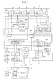
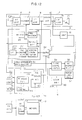
- Fig. 1 is block diagram showing one embodiment of the present invention.
- the embodiment shown is an example of an FM radio receiver.
- the FM receiver 1 comprises an antenna 2.
- a high frequency signal received by the antenna 2 is amplified by a high frequency amplifier 4.
- the output of the high frequency amplifier 4 is applied to an mixer 6.
- the mixer 6 is also connected to receive a local oscillation signal from a voltage controlled oscillator 26 serving as a local oscillator. As a result, the output of the mixer 6 becomes an intermediate frequency signal.
- the intermediate frequency signal obtained from the mixer 6 is amplified by an intermediate frequency amplifier 8 and the amplified intermediate frequency signal is detected by an FM detecting circuit 10 including a frequency discriminator.
- the output of the detecting circuit 10 is amplified by a low frequency amplifier 12 and the amplified low frequency signal is applied to a speaker 14, thereby to produce a sound.
- a block 3 encircled with the dotted line shows an automatic frequency control loop operable following an S curve signal and a block 5 encircled with the two dotted line shows a phase locked loop.
- the automatic frequency control loop 3 comprises an amplifier 16 for amplifying an S curve signal obtained from the FM detector 10.
- the output voltage Vs obtained from the amplifier 16 is applied to a window comparator 18 having two different threshold levels.
- the two outputs of the window comparator 18 are applied to a second charge pump 20.
- the second charge pump generates 3-value digital signals associated with the output voltage Vs from the window comparator 18, i.e. the high level of the first state, the low level of the second state and the high impedance of the third state.
- the window comparator 18 and the second charge pump 20 will be described in more detail subsequently with reference to Figs. 4 and 5.
- the output of the second charge pump 20 is applied to a switch circuit 22.
- the phase locked loop 5 comprises a frequency divider 28 connected to receive the output from the local oscillator, i.e. the voltage controlled oscillator 26.
- the frequency divider 28 is referred to as a prescaler and is adapted to frequency divide the local oscillation signal at a fixed frequency division ratio, say .
- the output of the frequency divider 28 is applied to a programmable frequency divider 30.
- the programmable frequency divider 30 is supplied with the frequency division ratio data from an "N" value generator 48 included in a control circuit 11, to be described subsequently, thereby to frequency divide the signal obtained from the fixed frequency divider 28 in accordance with the above described frequency division ratio data.
- the output of the programmable frequency divider 30 is applied to a phase comparator 32 as a frequency signal fp.
- the phase comparator 32 is connected to receive, as a reference frequency signal fo, the output from a reference oscillator 34 of such as a crystal controlled oscillator.
- the phase comparator 32 compares the phases of these two signals fp and fo, thereby to provide a signal associated with the phase reference to the first charge pump 36.
- the first charge pump 36 provides the 3-value digital signals, i.e. the high level of the first state, the low level of the second state and the high impedance of the third state.
- the phase comparator 32 and the first charge pump 36 will be also described in more detail subsequently with reference to Figs. 2 and 3.
- the output of the first charge pump 36 is applied to the switch circuit 22.
- the switch circuit 22 is responsive to the signal P/S obtained from a P/S signal generator 50 included in the control circuit 11 to be described subsequently, thereby to select the digital signal from the first charge pump 36 or the digital signal from the second charge pump 20 to provide the same to a low-pass filter 24.
- the signal P/S will be described in more detail subsequently, the same is provided as two value signals, so that the switch circuit 22 is switched to apply the digital signal from the second charge pump to the low-pass filter 24 on the occasion of reception of a broadcasting wave by the receiver 1.
- the low-pass filter 24 provides a direct current voltage responsive to the digital signal obtained from the first charge pump 36 or the second charge pump 20 through the switch circuit 22 and the above described direct current voltage is applied as a tuning voltage or a control voltage to the high frequency amplifier 4 and the voltage controlled oscillator 26.
- the phase comparator 32 (or the first charge pump 36) included in the phase locked loop 5 is connected to a lock detecting circuit 38, so that the lock detecting circuit 38 may detect whether the phase locked loop 5 is locked.
- the lock detecting circuit 38 may be of such a type as disclosed in United States Patent No. 4,201,945, issued May 6, 1980 to Ohgishi et al. and assigned to the same assignee as the present invention. Basically, the lock detecting circuit 38 is adapted to provide a lock detected output signal LOCK responsive to absence of the phase difference between two signals fp and fo.
- a channel key 7 is provided for selection of station by the FM receiver 1.
- the channel key 7 comprises a plurality of keys for selecting a plurality of channels and the operation signal is applied to a memory circuit 9.
- the memory circuit 9 comprises an address decoder 42 and a memory 44.
- the memory 44 is implemented by a programmable read only memory, for example, so that the frequency division ratio data may be stored for the respective channels.
- an upward key 13 and a downward 15 and a memory key 17 are provided.
- the operation signals of these three keys 13, 15 and 17 are applied to the control circuit 11.
- the control circuit 11 comprises a read/write controller 46 and an "N" value generator 48.
- the "N" value generator 48 comprises a presettable up/down counter, for example.
- the read/write controller 46 Upon operation of the memory key 17, the read/write controller 46 is placed in a writing mode. Accordingly, the "N" value obtained from the "N” value generator 48 is stored in the address of the memory 44 designated by the channel key 7 and thus by the address decoder 48.
- the channel key 7 When the channel key 7 is operated to select the station of a desired channel, the corresponding address of the memory 44 is designated by the address decoder 42 and the frequency division ratio data is read out from the address and the same is preset in the "N" value generator 48 through the read/write controller 48.
- the frequency division ratio data obtained from the memory 44 is set in the programmable frequency divider 30.
- the "N" value from the "N” value generator 48 may be renewed (incremented or decremented) and set in the programmable frequency divider 30 through operation of the upward key 13 or the downward key 15 rather than utilizing the channel key 7.
- the control circuit 11 further comprises P/S signal generator 50.
- the P/S signal generator 50 is responsive to the signal SD from the tuning detecting circuit 40, the signal LOCK from the lock detecting circuit 38, and a signal PLL-SET to be described subsequently to change the state of the signal P/S. Meanwhile, a circuit for generating the signal PLL-SET will be described in more detail subsequently with reference to Fig. 8.
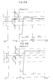
- the phase comparator 32 has two input terminals 321 and 322, which are connected to receive the reference frequency signal fo from the reference oscillator 34 and the frequency signal fp from the programmable frequency divider 30, respectively.
- the phase comparator 32 comprises two delay flip-flops 323 and 324, which have clock terminals CL1 and CL2, reset terminals Rl and R2, data terminals Dl and D2, and output terminals Ql, Ql and Q2, Q2, respectively.
- the reference frequency signal fo is applied to the clock terminal CL1 of the delay flip- flop 323 and is also applied to the reset terminal R2 of the delay flip-flop 324.
- the frequency signal fp the phase of which is to be compared is applied to the clock terminal CL2 of the delay flip-flop 324 and is also applied to the reset terminal Rl of the delay flip-flop 323.
- the output terminal Ql is connected to the data terminal D2 and the output terminal Q2 is connected to the data terminal Dl.
- the output terminal Ql of the delay flip-flop 323 is connected to the gate electrode of a P channel field effect transistor 361 constituting the charge pump 36.
- the output terminal Q2 of the delay flip-flop 324 is connected to the gate electrode of an N channel field effect transistor 362 included in the charge pump 36.
- the charge pump 36 comprises a series connection of the above described two field effect transistors 361 and 362. One end of the above described series connection is connected to the ground level and the other end of the above described series connection is connected to the positive source voltage V DD* The junction of the field effect transistors 361 and 362 is connected to the output terminal 363 of the charge pump 36.
- the delay flip-flops 323 and 324 used in the embodiment shown will operate in the following manner. More specifically, these delay flip-flops are operable responsive to the rise of the clock applied to the clock terminals CL and make no change of the output Q responsive to the fall of the clock signal. On the occasion of the rise of the clock, if the signal at the data terminal D is the logic one, the output Q becomes the logic one, and conversely on the occasion of the fall of the clock, if the signal at the data terminal D is the logic zero, the output Q becomes the logic zero.
- the output Q2 of the delay flip-flop 324 becomes the logic one. Since at that time the clock terminal CL1 of the delay flip-flop 323 has not been supplied with the rise of the input signal fo, the output terminal Ql of the flip-flop 323 remains the logic zero and the output terminal Ql of the flip-flop 323 remains the logic one. Accordingly, in such state the N channel field effect transistor 362 included in the charge pump 36 is rendered in a conductive state, while the P channel field effect transistor 361 of the charge pump 36 remains in a non-conductive state. Therefore, the output terminal 363 of the charge pump 36 becomes the low level state.
- the delay flip-flop 323 does not make any storing state, since the same has been reset responsive to the previous signal fp. Furthermore, the delay flip-flop 324 is reset responsive to the rise of the signal fo and at that timing the output terminal Q2 turns to the logic zero. Accordingly, the N channel field effect transistor 362 included in the charge pump 36 returns again to a nonconductive state. More specifically, during a time period when the output Q2 of the delay flipflop 324 is the logic one, the output terminal 363 of the charge pump 36 exhibits the low level state.
- the output terminal Q2 of the delay flip-flop 324 becomes the logic one.
- the delay flip-flop 324 is reset and the output terminal Q2 becomes the logic zero.
- the clock terminal CL1 of the delay flip-flop 323 is supplied with the rise of the signal fo, the delay flip-flop 323 has been supplied, at the data terminal Dl, with the logic zero of the output terminal Q2 before the delay flip-flop 324 is reset and therefore the output terminal Ql remains the logic zero.
- the N channel field effect transistor 362 included in the charge pump 36 is placed in a conductive state and the output terminal 363 becomes the low level.
- the signal fo has advanced in terms of the phase as compared with the input signal fp as at the timing t3 in Fig. 3. Since the delay flip-flop 323 has been supplied, at the data terminal Dl, with the logic one of the output Q2 of the delay flip-flop 324, the output terminal Ql becomes the logic one at the timing t6 and the output terminal Ql becomes the logic zero. Accordingly, the P channel field effect transistor 361 included in the charge pump 36 is placed in a conductive state. On the other hand, the output terminal Q2 of the flip-flop 324 remains the logic zero and the N channel field effect transistor 362 included in the charge pump 36 remains in a non-conductive state.
- the delay flip-flop 323 When the signal fp rises at the timing t7, the delay flip-flop 323 is reset and accordingly the output Ql becomes the logic one. Therefore, the P channel field effect transistor 361 returns to a non-conductive state. More specifically, during a time period when the output terminal Ql of the delay flip-flop 323 is the logic zero, the P channel field effect transistor 361 included in the charge pump 36 is rendered conductive and the output terminal 363 exhibits the high level state.
- the 3-value digital signals are obtained from the output terminal 363 of the charge pump 36 responsive to the phase difference between the input signals fo and fp.
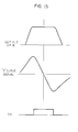
- the S curve signal from the frequency discriminator included in the FM detecting circuit 10 is amplified by the amplifier 16 and is applied, as the voltage Vs, to the input 181 of the window comparator 18.
- the window comparator 18 comprises two operational amplifiers 182 and 183, wherein the S curve signal voltage Vs is applied to one input (-) of each of the operational amplifiers 182 and 183.
- the window comparator 18 comprises a voltage dividing circuit comprising a series connection of three resistors 184, 185 and 186, and the voltage across the resistor 185, i.e.
- the second charge pump 20 may be structured in the same manner as the previously described first charge pump 36 and comprises a series connection of a P channel field effect transistor 201 and an N channel field effect transistor 202, the junction of which is connected to the output terminal 203. Meanwhile, the terminal voltages Vs L and V SH of the resistor 185 are the threshold value levels of the window comparator 18 and is selected such that Vs L > Vs H .
- the output of the operational amplifier 182 is applied, as the signal SL, to the gate electrode of the P channel field effect transistor 201 and the output of the operational amplifier 183 is applied, as the signal SH, to the gate electrode of the N channel field effect transistor 202.
- the S curve signal as shown in Fig. 5 is applied as the voltage signal Vs.
- the two threshold values Vs L and Vs H have been set as shown in Fig. 5.
- the output signals SL and SH of the operational amplifiers 182 and 183 both are the low level. Accordingly, the P channel field effect transistor 201 included in the charge pump 21 is rendered conductive and the N channel field effect transistor 202 included in the charge pump 20 is rendered non-conductive. Accordingly, the output terminal 203 of the charge pump 20 exhibits the high level state as shown in Fig. 5.
- the output signal SL of the operational amplifier 182 becomes the high level but the output SH of the operational amplifier 183 becomes the low level. Accordingly, the P channel field effect transistor 201 and the N channel field effect transistor 202 included in the charge pump 20 both are rendered non-conductive. Therefore, the output terminal 203 of the charge pump 24 exhibits the high impedance state.
- the outputs SL and SH of the two operational amplifiers 182 and 183 both are the high level. Accordingly, the P channel field effect transistor 201 included in the charge pump 20 is rendered non-conductive and the N channel field effect transistor 202 included in the charge pump 20 is rendered conductive. Therefore, the output terminal 203 of the charge pump 20 exhibits the low level state in such situation.
- the charge pump 20 generates the 3-value digital signals in association with the S curve signal voltage Vs.
- the digital signal obtained from the first charge pump 36 and the digital signal obtained from the second charge pump 20 both are applied to the switch circuit 22 as shown in Fig. 6.
- the switch circuit 22 comprises two analog gates 221 and 222.
- the analog gates 221 and 222 each comprise a parallel connection of complimentary MOS field effect transistors and are connected such that the analog gate 221 receives the output of the first charge pump 36 and the analog gate 22 receives the output of the second charge pump 20.
- the outputs of the respective analog gates 221 and 222 are commonly connected to the low-pass filter 24.
- the signal P/S from the P/S signal generator (Fig. 7) is applied to the switch circuit 22 as a control signal thereof.
- the switch circuit 22 is structured such that the signal P/S is received by means of a combination of three inverters 223, 224 and 225 so that the analog gate 221 is rendered conductive when the signal P/S is the high level and the analog gate 222 is rendered conductive when the signal P/S is the low level.
- Fig. 7 is a schematic diagram showing the P/S signal generator 50 included in the control circuit 11.
- the P/S signal generator 50 comprises a two-input AND gate 501.
- One input of the AND gate 501 is connected to receive the detected signal SD obtained from the tuning detecting circuit 40 and the other input is connected to receive the lock detected signal LOCK obtained from the lock detecting circuit 38.
- the output of the AND gate 501 is applied to the reset terminal R of a set preferential flip-flop 504.
- the signal SD is inverted by an inverter 502 and the inverted output is applied to one input of a two-input OR gate 503.
- the other input of the OR gate 503 is connected to receive the signal PLL-SET (Fig.
- the signal PLL-SET is obtained from a circuit as shown in Fig. 8. More specifically, the operation signals of the channel key 7 serving as a station selecting means and of the upward key 13 and the downward key 15 are applied through an OR gate 19 to the trigger input of a monostable multivibrator 21. More specifically, the monostable multivibrator 21 is responsive to the rise of the output of the OR gate 19 to provide the signal PLL-SET which lasts for a predetermined time period. Accordingly, it would be appreciated that the signal PLL-SET assumes the high level or the logic one when station selection is commanded by means of the station selecting means.
- the P/S signal generator 50 shown in Fig. 7 operates such that station selection is commanded by means of the keys 7, 13 or 15 the flip-flop 504 is set and the non-inverted output 9, i.e. the signal P/S becomes the high level or the logic one.
- the flip-flop 504 is reset and accordingly the signal P/S turns to the low level.
- the P/S signal generator 50 generates the signal P/S representing whether the receiver 1 is in a state of receiving a desired broadcasting wave.
- Fig. 9 shows in detail the low-pass filter 24.
- the low-pass filter 24 receives the signal from the switch circuit 22, i.e. the digital signal obtained from the charge pump 36 or 20.
- an electric charge storage means i.e. a capacitor 243 is charged through resistors 241 and 242. Accordingly, the output voltage of the low-pass filter 24, i.e. the tuning voltage or the control voltage increases.
- the digital signal is the low level, the electric charge in the capacitor 243 is discharged, so that the output voltage of the low-pass filter 24 decreases.
- the capacitor 243 is neither charged nor discharged and accordingly the output voltage of the low-pass filter 24 maintains a constant state.
- a muting circuit is responsive to the station selecting command, so that the sound signal applied to the low frequency amplifier 12 is muted.
- the memory circuit 9 and/or the "N" value generator 48 are responsive to the operation of the key 7, 13 or 15 to -provide the frequency division ratio data to the programmable frequency divider 30. Accordingly the frequency division ratio data associated with the desired channel (frequency) is preset in the programmable frequency divider 30.
- the flip-flop 504 of the P/S signal generator 50 shown in Fig. 7 is set and the signal P/S becomes the high level or the logic one. Then only the analog gate 221 in the switch circuit 22 (Fig. 6) is rendered conductive while the other gate 222 is rendered non-conductive. Accordingly, the output of the first charge pump 36 is applied to the low-pass filter 24, whereby the phase locked loop is established. Therefore, the output voltage of the low-pass filter 24 increases as shown in Fig. 10A by means of the phase comparator 32 and the first charge pump 36. More specifically, after the timing t12 in Fig.
- the output of the first charge pump 36 becomes the high level and the capacitor 243 of the low-pass filter 24 (Fig. 9) is charged. Accordingly, the frequency of the voltage controlled oscillator 26 increases.
- the signal SD as shown in Fig. 10A is obtained from the tuning detecting circuit 40 receiving the output voltage obtained from the intermediate frequency amplifier 8 (Fig. 1).
- the PLL loop 5 reaches a stabilized state at the timing tl3 in Fig. 10A and the signal LOCK is obtained from the lock detecting circuit 38 at the timing tl3. Accordingly, the output is obtained from the AND gate 501 of the P/S signal generator 50 shown in Fig. 7 and the flip-flop 504 is reset.
- the output Q of the flip-flop 504, i.e. the signal P/S turns to the low level.
- the analog gate 221 in the switch circuit 22 (Fig. 6) is closed and only the analog gate 222 is rendered conductive.
- the digital signal from the second charge pump 20 is applied through the switch circuit 22 to the low-pass filter 24.
- the automatic frequency control loop 13 operable following the S curve signal is established. Since the capacitor 243 (Fig. 9) of the low-pass filter 24 has been charged at that time due to the previous operation of the phase locked loop 5, the automatic frequency control loop 3 initiates an automatic frequency control operation based on the electric charge in the capacitor 243 at that time. Accordingly, a broadcasting wave of the frequency as selected by the phase locked loop 5 is kept received. Then the automatic frequency control operation is continued by means of the previously described window comparator 18 and the second charge pump 20.
- the frequency division ratio data corresponding to the channel is set in the programmable frequency divider 30, like the previously described Fig. l0A case, whereby the phase locked loop 5 is established; however, since there is no broadcasting wave in the channel, no signal SD is obtained at the selected channel. Therefore, the signal P/S obtained from the P/S signal generator 50 maintains the high level and accordingly the switch circuit 20 is kept switched to the side of the phase locked loop 5.
- the automatic frequency control loop 3 operable following the S curve signal will not operate due to the fact that there is no broadcasting wave in the selected channel.
- the signal SD from the tuning detecting circuit 40 has turned to the low level for some reasons in the course of the tuning control operation by means of the automatic frequency control loop 3 as shown in Fig. 10A, such as because the electric field intensity of the broadcasting wave has become weak, a power source voltage suddenly fluctuates and so on.
- the signal SD is inverted by the inverter 502 shown in Fig. 7 to become the high level, so that the flip-flop 504 is set. Therefore, the output of the flip-flop 504, i.e. the signal P/S becomes the high level.
- the switch circuit 22 is controlled to provide the digital signal from the first charge pump 36 to the low-pass filter 24, so that again the phase locked loop 5 is established and again the tuning control operation is performed by means of the phase locked loop 5.
- the tuning control operation by means of the automatic frequency control loop 3 operable following the S curve signal is performed, as described previously.
- Fig. 11 is a diagram showing another embodiment of the present invention.
- the Fig. 11 embodiment is adapted to disable the prescaler or the fixed frequency divider 28 when the signal P/S from the P/S signal generator 50 becomes the low level, i.e. the automatic frequency control loop 3 is established.
- a switching transistor 25 is interposed in a voltage source line 281 and the signal P/S is applied to the base electrode of the switching transistor 25.
- the switching transistor 25 is rendered conductive. Therefore, the voltage source line 281 of the frequency divider 28 receives a voltage V DD through the switching transistor 25.
- the phase locked loop 5 normally operates. Conversely, when the signal P/S turns to the low level, the switching transistor 25 is rendered non-conductive and the voltage source line 281 is interrupted. Therefore, the operation of the frequency divider 28 is stopped or disabled.
- the fact that the signal P/S is the low level means that the FM receiver 1 is in a state of receiving a desired broadcasting wave and accordingly in such a case the tuning control operation is performed by the automatic fine control loop 3.
- an interference due to harmonics from the frequency divider 28 is removed by disabling the operation of the frequency divider 28 included in the phase locked loop 5, whereby an improved signal to noise ratio can be attained.
- Fig. 12 is a block diagram showing a further embodiment of the present invention.
- the embodiment shown is substantially the same as the Fig. 1 embodiment, except for the following respects. More specifically, the Fig. 12 embodiment is structured such that the S curve signal from the FM detector 10 including a frequency discriminator is amplified by the amplifier 16 and is applied to the switch circuit 22 as the voltage Vs and the switch circuit 22 is connected to receive the digital signal from the first charge pump 36, and the window comparator 18' and the second charge pump 20' are interposed between the switch circuit 22 and the low-pass filter 24.
- the window comparator 18' and the second charge pump 20' are also included in the phase locked loop 5.
- the Fig. 12 is structured such that the S curve signal from the FM detector 10 including a frequency discriminator is amplified by the amplifier 16 and is applied to the switch circuit 22 as the voltage Vs and the switch circuit 22 is connected to receive the digital signal from the first charge pump 36, and the window comparator 18' and the second charge pump 20' are interposed between the switch circuit 22 and
- the window comparator 18' and the second charge pump 20' merely function as a voltage converting means when the phase locked loop 5 is established. Accordingly, the Fig. 12 embodiment also performs the effect and operation of the present invention that the tuning control operation is performed by the phase locked loop 5 during the station selection and after once the broadcasting wave is received the tuning control operation is performed by the automatic frequency control loop 3 operable following the S curve signal.
- Fig. 13 is a block diagram showing still a further embodiment of the present invention.
- the Fig. 13 embodiment is also substantially the same as the Fig. 1 embodiment, except for the following respects. More specifically, whereas the Fig. 1 embodiment was structured to commonly use the low-pass filter 24 in both the automatic frequency control loop 3 and the phase locked loop 5, the Fig. 13 embodiment is structured such that separate low-pass filters 24' and 24" are interposed in the automatic frequency control loop 3 and the phase locked loop 5, respectively.
- the outputs of the low-pass filters 24' and 24" are selected by the switch circuit 22 and the selected output is applied as a tuning voltage or a control voltage to the high frequency amplifier 4 and the voltage controlled oscillator 26.
- a charge transfer circuit 52 is provided between the low-pass filters 24' and 24".
- the charge transfer circuit 52 is structured such that when the signal P/S turns to the low level an electric charge is transferred from one low-pass filter 24' to the other low-pass filter 24".
- the tuning control operation can be performed based on the tuning voltage or the control voltage obtained by the phase locked loop 5.
- the charge transfer circuit 52 may be structured such that when the signal P/S turns from the low level to the high level the electric charge in the low-pass filter 24" is transferred to the other low-pass filter 24'.
- Fig. 14 is a block diagram for depicting another example of the tuning detecting circuit.
- the tuning detecting circuit 40' of the Fig. 14 embodiment is connected to receive the output of the intermediate frequency amplifier 8 and the output of the FM detector 10.
- the signal SD is generated responsive to the output of the intermediate frequency amplifier 8 and the S curve signal of the detector 10.
- the signal SD was generated only responsive to the output of the intermediate frequency amplifier 8.
- the lock detecting circuit 38 was provided in the phase locked loop 5, so that the flip-flop 504 (Fig. 7) was reset by the detected output signal LOCK and the output signal SD of the tuning detecting circuit 40 (40').
- the signal LOCK may be replaced by the signal LOCK' obtained from the timer 28 shown in Fig. 8. More specifically, in the previously described embodiments, the signal P/S was turned to the low level, provided that the phase locked loop 5 has reached a locked state.
- the phase locked loop 5 surely reaches a stabilized state after the lapse of a predetermined time period, say 0.5 second, at the least after the station selection is commanded, and based on such consideration the lock detecting circuit 38 can be dispensed with, by substituting a timer 23 of a simple structure for the lock detecting circuit 38.
- a timer 23 of a simple structure for the lock detecting circuit 38.
- the present invention was described in conjunction with several embodiments embodied in an FM receiver. However, it is pointed out that the present invention can also be applied to an AM receiver. Since the AM receiver does not comprise a frequency discriminator, in practicing the present invention in an AM receiver it becomes necessary to provide a frequency discriminator for discriminating the frequency of the intermediate frequency signal. By applying the output of such frequency discriminator to the input of the amplifier 16, for example, an automatic frequency control loop operable following the S curve signal can be implemented in an AM receiver.
Landscapes
- Engineering & Computer Science (AREA)
- Computer Hardware Design (AREA)
- Microelectronics & Electronic Packaging (AREA)
- Stabilization Of Oscillater, Synchronisation, Frequency Synthesizers (AREA)
- Channel Selection Circuits, Automatic Tuning Circuits (AREA)
- Superheterodyne Receivers (AREA)
Applications Claiming Priority (2)
| Application Number | Priority Date | Filing Date | Title |
|---|---|---|---|
| JP13398679A JPS5657324A (en) | 1979-10-16 | 1979-10-16 | Digital electronic tuning system |
| JP133986/79 | 1979-10-16 |
Publications (2)
| Publication Number | Publication Date |
|---|---|
| EP0028100A1 true EP0028100A1 (de) | 1981-05-06 |
| EP0028100B1 EP0028100B1 (de) | 1984-03-07 |
Family
ID=15117705
Family Applications (1)
| Application Number | Title | Priority Date | Filing Date |
|---|---|---|---|
| EP80303648A Expired EP0028100B1 (de) | 1979-10-16 | 1980-10-15 | Abstimmgerät für Empfänger |
Country Status (4)
| Country | Link |
|---|---|
| US (1) | US4394778A (de) |
| EP (1) | EP0028100B1 (de) |
| JP (1) | JPS5657324A (de) |
| DE (1) | DE3066856D1 (de) |
Cited By (7)
| Publication number | Priority date | Publication date | Assignee | Title |
|---|---|---|---|---|
| EP0042728A1 (de) * | 1980-06-17 | 1981-12-30 | Sanyo Electric Co., Ltd. | Abstimmsteuergerät eines Empfängers mit elktronischer Abstimmeinheit |
| EP0075332A3 (de) * | 1981-09-23 | 1983-09-07 | Siemens Aktiengesellschaft | Empfängerschaltung |
| EP0367214A1 (de) * | 1988-11-02 | 1990-05-09 | Deutsche Thomson-Brandt GmbH | Satelliten-Rundfunkempfänger |
| US5517678A (en) * | 1988-11-02 | 1996-05-14 | Deutsche Thomson-Brandt Gmbh | Satellite radio receiver |
| EP0928060A1 (de) * | 1997-12-31 | 1999-07-07 | Koninklijke Philips Electronics N.V. | Gleichspannungswandler mit verbessertem Wirkungsgrad |
| EP1912333A1 (de) * | 2003-12-12 | 2008-04-16 | QUALCOMM Incorporated | Phasenregelschleife mit automatischer Verstärkungseinstellung |
| US7825706B2 (en) | 2002-06-28 | 2010-11-02 | Qualcomm Incorporated | Phase locked loop that sets gain automatically |
Families Citing this family (12)
| Publication number | Priority date | Publication date | Assignee | Title |
|---|---|---|---|---|
| JPS62117408A (ja) * | 1985-11-18 | 1987-05-28 | Casio Comput Co Ltd | オ−トチユ−ニング装置 |
| US4903329A (en) * | 1987-06-15 | 1990-02-20 | Motorola, Inc. | Clamping circuit for a PLL tuning system |
| JP3036763B2 (ja) * | 1989-10-31 | 2000-04-24 | 三洋電機株式会社 | Amラジオ受信機 |
| WO1994028682A2 (en) * | 1993-05-24 | 1994-12-08 | Alexandr Mikhailovich Vasiliev | All-wave television channel selector with frequency synthesizer |
| JPH07273294A (ja) * | 1994-03-31 | 1995-10-20 | Fujitsu Ltd | 半導体装置 |
| JP4219436B2 (ja) * | 1998-02-17 | 2009-02-04 | 富士通株式会社 | チューナ装置 |
| US6775344B1 (en) | 1999-04-02 | 2004-08-10 | Storage Technology Corporation | Dropout resistant phase-locked loop |
| KR100468360B1 (ko) * | 2002-07-25 | 2005-01-27 | 인티그런트 테크놀로지즈(주) | 수신 장치의 선형성 개선을 위한 하모닉 회로 |
| US7539170B2 (en) * | 2003-12-29 | 2009-05-26 | Research In Motion Limited | Optimized data reconnect |
| JP4325490B2 (ja) | 2004-06-10 | 2009-09-02 | 株式会社デンソー | ヘテロダイン受信機 |
| US20090080559A1 (en) * | 2005-05-11 | 2009-03-26 | Michael Armbruster | Antenna diversity by means of its through connection for receivers of digital radio signals |
| US7755437B2 (en) * | 2005-08-24 | 2010-07-13 | Qualcomm Incorporated | Phase locked loop system having locking and tracking modes of operation |
Citations (5)
| Publication number | Priority date | Publication date | Assignee | Title |
|---|---|---|---|---|
| FR2331917A1 (fr) * | 1975-11-14 | 1977-06-10 | Rca Corp | Synthetiseur de frequences de television pour des porteuses non standards |
| US4031549A (en) * | 1976-05-21 | 1977-06-21 | Rca Corporation | Television tuning system with provisions for receiving RF carrier at nonstandard frequency |
| US4077008A (en) * | 1976-10-18 | 1978-02-28 | Rca Corporation | Phase locked loop tuning system with station scanning provisions |
| US4078212A (en) * | 1976-02-27 | 1978-03-07 | Rca Corporation | Dual mode frequency synthesizer for a television tuning apparatus |
| US4109283A (en) * | 1976-05-21 | 1978-08-22 | Rca Corporation | Frequency counter for a television tuning system |
Family Cites Families (3)
| Publication number | Priority date | Publication date | Assignee | Title |
|---|---|---|---|---|
| US3962640A (en) * | 1974-09-09 | 1976-06-08 | Texas Instruments Incorporated | Frequency selection and control |
| US4023116A (en) * | 1976-07-08 | 1977-05-10 | Fairchild Camera And Instrument Corporation | Phase-locked loop frequency synthesizer |
| US4262364A (en) * | 1978-02-27 | 1981-04-14 | Tokyo Shibaura Denki Kabushiki Kaisha | Electronic digital channel-selecting apparatus |
-
1979
- 1979-10-16 JP JP13398679A patent/JPS5657324A/ja active Granted
-
1980
- 1980-10-14 US US06/196,272 patent/US4394778A/en not_active Expired - Lifetime
- 1980-10-15 DE DE8080303648T patent/DE3066856D1/de not_active Expired
- 1980-10-15 EP EP80303648A patent/EP0028100B1/de not_active Expired
Patent Citations (6)
| Publication number | Priority date | Publication date | Assignee | Title |
|---|---|---|---|---|
| FR2331917A1 (fr) * | 1975-11-14 | 1977-06-10 | Rca Corp | Synthetiseur de frequences de television pour des porteuses non standards |
| GB1561544A (en) * | 1975-11-14 | 1980-02-20 | Rca Corp | Tuning apparatus for radio frequency especially television receivers |
| US4078212A (en) * | 1976-02-27 | 1978-03-07 | Rca Corporation | Dual mode frequency synthesizer for a television tuning apparatus |
| US4031549A (en) * | 1976-05-21 | 1977-06-21 | Rca Corporation | Television tuning system with provisions for receiving RF carrier at nonstandard frequency |
| US4109283A (en) * | 1976-05-21 | 1978-08-22 | Rca Corporation | Frequency counter for a television tuning system |
| US4077008A (en) * | 1976-10-18 | 1978-02-28 | Rca Corporation | Phase locked loop tuning system with station scanning provisions |
Cited By (9)
| Publication number | Priority date | Publication date | Assignee | Title |
|---|---|---|---|---|
| EP0042728A1 (de) * | 1980-06-17 | 1981-12-30 | Sanyo Electric Co., Ltd. | Abstimmsteuergerät eines Empfängers mit elktronischer Abstimmeinheit |
| US4476580A (en) * | 1980-06-17 | 1984-10-09 | Sanyo Electric Co., Ltd. | Automatic continuous tuning control apparatus for a receiver |
| EP0075332A3 (de) * | 1981-09-23 | 1983-09-07 | Siemens Aktiengesellschaft | Empfängerschaltung |
| EP0367214A1 (de) * | 1988-11-02 | 1990-05-09 | Deutsche Thomson-Brandt GmbH | Satelliten-Rundfunkempfänger |
| WO1990005410A1 (de) | 1988-11-02 | 1990-05-17 | Deutsche Thomson-Brandt Gmbh | Satelliten-rundfunkempfänger |
| US5517678A (en) * | 1988-11-02 | 1996-05-14 | Deutsche Thomson-Brandt Gmbh | Satellite radio receiver |
| EP0928060A1 (de) * | 1997-12-31 | 1999-07-07 | Koninklijke Philips Electronics N.V. | Gleichspannungswandler mit verbessertem Wirkungsgrad |
| US7825706B2 (en) | 2002-06-28 | 2010-11-02 | Qualcomm Incorporated | Phase locked loop that sets gain automatically |
| EP1912333A1 (de) * | 2003-12-12 | 2008-04-16 | QUALCOMM Incorporated | Phasenregelschleife mit automatischer Verstärkungseinstellung |
Also Published As
| Publication number | Publication date |
|---|---|
| JPS627728B2 (de) | 1987-02-19 |
| EP0028100B1 (de) | 1984-03-07 |
| US4394778A (en) | 1983-07-19 |
| DE3066856D1 (en) | 1984-04-12 |
| JPS5657324A (en) | 1981-05-19 |
Similar Documents
| Publication | Publication Date | Title |
|---|---|---|
| EP0028100A1 (de) | Abstimmgerät für Empfänger | |
| US4365349A (en) | Radio receiver having phase locked loop and automatic frequency control loop for stably maintaining local oscillator frequency of voltage-controlled local oscillator | |
| EP0011128A1 (de) | Digitale Phasenvergleichsanordnung | |
| US5315623A (en) | Dual mode phase-locked loop | |
| US3611152A (en) | Stabilized automatic tuning receiver | |
| EP0042728A1 (de) | Abstimmsteuergerät eines Empfängers mit elktronischer Abstimmeinheit | |
| US4232393A (en) | Muting arrangement of a radio receiver with a phase-locked loop frequency synthesizer | |
| KR960000523B1 (ko) | 수신기 | |
| US3980968A (en) | Non-proportionate AFC system | |
| KR0158187B1 (ko) | 위성 방송 수신기 | |
| JPH0149051B2 (de) | ||
| GB2048002A (en) | Frequency control for pll receiver systems | |
| GB1483626A (en) | Broadcast receiver tuning circuit | |
| US4245351A (en) | AFT Arrangement for a phase locked loop tuning system | |
| US4337486A (en) | Synchronizing signal discriminator for use in channel selection apparatus of television receiver | |
| JPS6141458B2 (de) | ||
| DK163622C (da) | Afstemningssystem til automatisk afstemning af en tuner i et fjernsynsmodtageapparat | |
| US4262364A (en) | Electronic digital channel-selecting apparatus | |
| US3987399A (en) | Radio receiver | |
| KR920008656B1 (ko) | Afc 장치 | |
| GB2173661A (en) | Superheterodyne television tuner | |
| US4796102A (en) | Automatic frequency control system | |
| US3218571A (en) | Electronic servo controlled automatic frequency scanning system | |
| KR840000227B1 (ko) | 수신기의 동조제어장치 | |
| EP0007914A1 (de) | Handbetriebene abstimmvorrichtung |
Legal Events
| Date | Code | Title | Description |
|---|---|---|---|
| PUAI | Public reference made under article 153(3) epc to a published international application that has entered the european phase |
Free format text: ORIGINAL CODE: 0009012 |
|
| AK | Designated contracting states |
Designated state(s): DE FR GB IT NL |
|
| 17P | Request for examination filed |
Effective date: 19811105 |
|
| ITF | It: translation for a ep patent filed | ||
| GRAA | (expected) grant |
Free format text: ORIGINAL CODE: 0009210 |
|
| AK | Designated contracting states |
Designated state(s): DE FR GB IT NL |
|
| REF | Corresponds to: |
Ref document number: 3066856 Country of ref document: DE Date of ref document: 19840412 |
|
| ET | Fr: translation filed | ||
| PLBE | No opposition filed within time limit |
Free format text: ORIGINAL CODE: 0009261 |
|
| STAA | Information on the status of an ep patent application or granted ep patent |
Free format text: STATUS: NO OPPOSITION FILED WITHIN TIME LIMIT |
|
| 26N | No opposition filed | ||
| ITPR | It: changes in ownership of a european patent |
Owner name: CESSIONE;SANYO ELECTRIC CO. LTD |
|
| REG | Reference to a national code |
Ref country code: FR Ref legal event code: TP |
|
| NLS | Nl: assignments of ep-patents |
Owner name: SANYO ELECTRIC CO., LTD. TE MORIGUCHI, JAPAN. |
|
| REG | Reference to a national code |
Ref country code: GB Ref legal event code: 732 |
|
| ITTA | It: last paid annual fee | ||
| PGFP | Annual fee paid to national office [announced via postgrant information from national office to epo] |
Ref country code: GB Payment date: 19931005 Year of fee payment: 14 |
|
| PGFP | Annual fee paid to national office [announced via postgrant information from national office to epo] |
Ref country code: FR Payment date: 19931011 Year of fee payment: 14 Ref country code: DE Payment date: 19931011 Year of fee payment: 14 |
|
| PGFP | Annual fee paid to national office [announced via postgrant information from national office to epo] |
Ref country code: NL Payment date: 19931031 Year of fee payment: 14 |
|
| PG25 | Lapsed in a contracting state [announced via postgrant information from national office to epo] |
Ref country code: GB Effective date: 19941015 |
|
| PG25 | Lapsed in a contracting state [announced via postgrant information from national office to epo] |
Ref country code: NL Effective date: 19950501 |
|
| GBPC | Gb: european patent ceased through non-payment of renewal fee |
Effective date: 19941015 |
|
| NLV4 | Nl: lapsed or anulled due to non-payment of the annual fee | ||
| PG25 | Lapsed in a contracting state [announced via postgrant information from national office to epo] |
Ref country code: FR Effective date: 19950630 |
|
| PG25 | Lapsed in a contracting state [announced via postgrant information from national office to epo] |
Ref country code: DE Effective date: 19950701 |
|
| REG | Reference to a national code |
Ref country code: FR Ref legal event code: ST |