EP0029350A2 - Ausgangstransistor für eine TTL-vorrichtung mit Trägerentladungsmitteln - Google Patents
Ausgangstransistor für eine TTL-vorrichtung mit Trägerentladungsmitteln Download PDFInfo
- Publication number
- EP0029350A2 EP0029350A2 EP80304070A EP80304070A EP0029350A2 EP 0029350 A2 EP0029350 A2 EP 0029350A2 EP 80304070 A EP80304070 A EP 80304070A EP 80304070 A EP80304070 A EP 80304070A EP 0029350 A2 EP0029350 A2 EP 0029350A2
- Authority
- EP
- European Patent Office
- Prior art keywords
- region
- diffusion
- base
- base region
- conductivity type
- Prior art date
- Legal status (The legal status is an assumption and is not a legal conclusion. Google has not performed a legal analysis and makes no representation as to the accuracy of the status listed.)
- Granted
Links
Images



Classifications
-
- H—ELECTRICITY
- H03—ELECTRONIC CIRCUITRY
- H03K—PULSE TECHNIQUE
- H03K19/00—Logic circuits, i.e. having at least two inputs acting on one output; Inverting circuits
- H03K19/02—Logic circuits, i.e. having at least two inputs acting on one output; Inverting circuits using specified components
- H03K19/08—Logic circuits, i.e. having at least two inputs acting on one output; Inverting circuits using specified components using semiconductor devices
- H03K19/082—Logic circuits, i.e. having at least two inputs acting on one output; Inverting circuits using specified components using semiconductor devices using bipolar transistors
- H03K19/088—Transistor-transistor logic
-
- H—ELECTRICITY
- H10—SEMICONDUCTOR DEVICES; ELECTRIC SOLID-STATE DEVICES NOT OTHERWISE PROVIDED FOR
- H10D—INORGANIC ELECTRIC SEMICONDUCTOR DEVICES
- H10D62/00—Semiconductor bodies, or regions thereof, of devices having potential barriers
- H10D62/10—Shapes, relative sizes or dispositions of the regions of the semiconductor bodies; Shapes of the semiconductor bodies
- H10D62/102—Constructional design considerations for preventing surface leakage or controlling electric field concentration
- H10D62/112—Constructional design considerations for preventing surface leakage or controlling electric field concentration for preventing surface leakage due to surface inversion layers, e.g. by using channel stoppers
-
- H—ELECTRICITY
- H10—SEMICONDUCTOR DEVICES; ELECTRIC SOLID-STATE DEVICES NOT OTHERWISE PROVIDED FOR
- H10D—INORGANIC ELECTRIC SEMICONDUCTOR DEVICES
- H10D62/00—Semiconductor bodies, or regions thereof, of devices having potential barriers
- H10D62/10—Shapes, relative sizes or dispositions of the regions of the semiconductor bodies; Shapes of the semiconductor bodies
- H10D62/17—Semiconductor regions connected to electrodes not carrying current to be rectified, amplified or switched, e.g. channel regions
- H10D62/177—Base regions of bipolar transistors, e.g. BJTs or IGBTs
-
- H—ELECTRICITY
- H10—SEMICONDUCTOR DEVICES; ELECTRIC SOLID-STATE DEVICES NOT OTHERWISE PROVIDED FOR
- H10D—INORGANIC ELECTRIC SEMICONDUCTOR DEVICES
- H10D84/00—Integrated devices formed in or on semiconductor substrates that comprise only semiconducting layers, e.g. on Si wafers or on GaAs-on-Si wafers
- H10D84/60—Integrated devices formed in or on semiconductor substrates that comprise only semiconducting layers, e.g. on Si wafers or on GaAs-on-Si wafers characterised by the integration of at least one component covered by groups H10D10/00 or H10D18/00, e.g. integration of BJTs
- H10D84/611—Combinations of BJTs and one or more of diodes, resistors or capacitors
- H10D84/613—Combinations of vertical BJTs and one or more of diodes, resistors or capacitors
- H10D84/615—Combinations of vertical BJTs and one or more of resistors or capacitors
-
- H—ELECTRICITY
- H10—SEMICONDUCTOR DEVICES; ELECTRIC SOLID-STATE DEVICES NOT OTHERWISE PROVIDED FOR
- H10D—INORGANIC ELECTRIC SEMICONDUCTOR DEVICES
- H10D84/00—Integrated devices formed in or on semiconductor substrates that comprise only semiconducting layers, e.g. on Si wafers or on GaAs-on-Si wafers
- H10D84/60—Integrated devices formed in or on semiconductor substrates that comprise only semiconducting layers, e.g. on Si wafers or on GaAs-on-Si wafers characterised by the integration of at least one component covered by groups H10D10/00 or H10D18/00, e.g. integration of BJTs
- H10D84/63—Combinations of vertical and lateral BJTs
-
- H—ELECTRICITY
- H10—SEMICONDUCTOR DEVICES; ELECTRIC SOLID-STATE DEVICES NOT OTHERWISE PROVIDED FOR
- H10W—GENERIC PACKAGES, INTERCONNECTIONS, CONNECTORS OR OTHER CONSTRUCTIONAL DETAILS OF DEVICES COVERED BY CLASS H10
- H10W10/00—Isolation regions in semiconductor bodies between components of integrated devices
- H10W10/01—Manufacture or treatment
- H10W10/031—Manufacture or treatment of isolation regions comprising PN junctions
-
- H—ELECTRICITY
- H10—SEMICONDUCTOR DEVICES; ELECTRIC SOLID-STATE DEVICES NOT OTHERWISE PROVIDED FOR
- H10W—GENERIC PACKAGES, INTERCONNECTIONS, CONNECTORS OR OTHER CONSTRUCTIONAL DETAILS OF DEVICES COVERED BY CLASS H10
- H10W10/00—Isolation regions in semiconductor bodies between components of integrated devices
- H10W10/30—Isolation regions comprising PN junctions
Definitions
- the present invention relates to a semiconductor device with a means for discharging carriers.
- TTL circuits are widely used for bipolar integrated circuits such as large scale integrated circuits (LSI) or very large scale integrated circuits (VLSI) for example because of their low power dissipation and because their speed of operation is faster than that of diode transistor logic (DTL) circuits.
- DTL diode transistor logic
- FIG. 1 of the accompanying drawings is a schematic circuit diagram.
- An output transistor of the circuit is designated by Tr l , and a multi-emitter input transistor by Tr 2 .
- This multi-emitter transistor Tr 2 performs the circuit's logic function, with inputs to the circuit being supplied to emitters of transistor Tr 2 .
- Resistor R L shown in Figure 1 is provided for discharging minority carriers stored in the base region of the transistor Tr 1 when output is switched from low level to high level, or from ON state to OFF state. This serves to improve the speed of operation when switching from ON to OFF.
- a semiconductor device with means for discharging carriers comprising a base region, of a first conductivity type, formed in a further region, of a second conductivity type, opposite to the first conductivity type, and a zone of the first conductivity type, characterised in that a diffusion region of the first conductivity type is formed between the base region and the said zone such as to provide an electrical connection between the base region and the said zone, for discharging carriers from the base region, when the potential of the base region bears a first relationship to (higher than or lower than) ' the potential of the further region, and such as to electrically isolate the base region from the said zone when the potential of the base region bears a second relationship to (lower than or higher than) the potential of the further region.
- An embodiment of this invention is suitable for performing high speed switching operations, and, for example, provides an improved structure for transistor-transistor logic TTL circuits.
- the inventors of the present invention In efforts to find a method for extracting base current (discharging carriers stored in the base) at the time of switching of an output transistor of a TTL circuit from ON state to OFF state, the inventors of the present invention theorized as follows: the characteristics required of a circuit or device used to draw out the base current in question are that practically no current is allowed to flow when the base potential is somewhat smaller than ON state potential, but a substantial amount of current is permitted to flow near the ON state potential.
- One embodiment of this invention relies on the fact that the inventors have found a way of fabricating a structure provided with a path for a leakage current in a region between the base of and an isolation diffusion zone provided for a transistor.
- Such a structure is realized by forming a p - diffusion in a region covering a part, or the whole, of the region between the base of and the isolation diffusion provided for a transistor.
- This p - diffusion has such an impurity concentration that it is pinched off by widening of a depletion layer when collector potential is at high level. When the collector (output) is at low level, however, widening of the depletion layer is small, so that the resistance of the diffusion is small, allowing the base current to be sufficiently discharged.
- Another embodiment of this invention provides a structure which, in relation to an output transistor, offers improved switching characteristics (without the provision of a resistor R L as shown in Figure 1), there being provided, in a region between the base region of an output transistor of a TTL circuit, and a semiconductor substrate (ground side zone) of the circuit, a diffusion which is doped in such a manner that it has the same conductivity sign as the base region but is doped more lightly than the base region.
- such an embodiment of this invention provides a structure in which, in relation to an output transistor of a TTL circuit there is a carrier path between the base of the transistor and ground zone which will turn ON and OFF in correspondence with ON and OFF states of the transistor, and whereby when the transistor is turned OFF from an ON state, carriers stored at the junction are vigorously discharged, thus improving switching speeds.
- a further embodiment provides a carrier path between a transistor base and an isolation diffusion zone , by means of a first diffusion region, extending between the base and the isolation diffusion zone and of the same conductivity type, with a second diffusion region of the opposite conductivity type over the first region and shorted to the collector.
- the transistor base is extended up to an isolation diffusion zone of the same conductivity type, with a diffusion region, of the opposite conductivity type, over the base region and shorted to the collector.
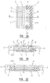
- FIG. 2A A plan view of an output transistor Tr1 according to one embodiment of the present invention is shown in Figure 2A, with Figure 2B and Figure 2C showing cross-sectional views along the lines B-B' and C-C' of Figure 2A.
- An n + layer 2 is buried in a p-type semiconductor substrate 1, and a p - diffusion 3 is formed.
- This p - diffusion 3 connects a p isolation diffusion 5 formed in an n-type epitaxial layer 4 and the p-type substrate to a p-type base region 6.
- a part of conventional collector region referenced (7) is thus replaced by the p - diffusion 3.
- n + emitter region 8 and an n + collector contact diffusion 9 there are formed an n + emitter region 8 and an n + collector contact diffusion 9, and a hollow part 10 within the base region 6 is a Shottky barrier diode SBD (which is shown in Figure 1) which serves the purpose of speeding up the switching operation when the output changes from low level to high level as is the case with resistor R L of Figure 1.
- SBD Shottky barrier diode
- p diffusion 3 is interposed between the p-type semiconductor substrate 1, the ground site, p isolation diffusion 5 and p-type base region 6.
- p diffusion 3 functions as a resistance conductor from the base to ground, and when the transistor Tr 1 is switched from ON to OFF (the output from low level to high level), carriers stored in the base region are caused to be discharged quickly through the p diffusion 3. This contributes to a high speed switching operation.
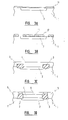
- an oxidized film 11 is formed on a p-type semiconductor substrate 1 by heat treatment at high temperature; a window is opened in the film 11, by a known photolithographic process, for fabricating a buried layer 2 by diffusion of antimony (Sb) or arsenic (As).
- oxide film 11 is reformed on the surface of buried layer 2 since the diffusion process is effected at high temperature.
- a photolithographic process is again effected to open windows at places where p - diffusions are to be formed, and suitable amounts of boron ions are implanted with a photoresist film 12 used in the process left as it is.
- the photoresist film 12 is completely removed, and the oxide film 11 is also removed using a solution of fluoric acid.
- epitaxial layer 4 is grown by a conventional vapour phase deposition. In this process, p diffusions 3 are diffused upwardly within the epitaxial layer 4 as shown because the diffusion coefficient of boron is large.
- the buried layer 2 is also diffused upwardly, but since the diffusion coefficient of antimony or arsenic is smaller than that of boron, the buried layer 2 is diffused less than p - diffusions 3.
- p isolation diffusions 5 areformed as shown in Figure 3D, and p-type base region 6 is also formed, both by conventional diffusion process.
- p - diffusions 3 are in contact with the base region 6 and isolation diffusions 5.
- transistor-transistor logic TTL circuit is further fabricated in accordance with prior art technology.
- p - diffusions 3 of an output transistor can easily be formed by implantation of boron ions before formation of epitaxial layer 4.
- This process of ion implantation as described above is the only process that is added to the prior art method of TTL fabrication. No other changes nor any other additions are required to manufacture the semiconductor device embodying the present invention described above.
- the resistance R L of the Figure 1 proposal must be formed separately, and to do so takes up chip area. Such a proposal is not in line with the recent trend towards increased packing density for integrated circuits.
- p diffusion 3 connects base 6 and isolation diffusion 5.
- the p - diffusion 3 is formed after formation of epitaxial layer 4.
- N A acceptor concentration in diffusion 3
- N D donor concentration in region 4
- q the electronic charge
- ⁇ o the permittivity of free space
- k s the relative permittivity of the material of the device of Figure 4 (e.g. silicon)
- ⁇ T the potential across the junction.
- the amount Q of impurities to be deposited in region 3 is:-
- n buried layer 22 is formed in a p-type silicon substrate 21, and n-type collector region 23, p isolation diffusion 24, p - diffusion 25, p-type base region 26, n + emitter region 27, n + diffusion 28, Shottky barrier diode (SBD) region 29, and collector contact diffusion 23A are fabricated in accordance with known techniques.
- SBD Shottky barrier diode
- the depletion layer extends from a first p-n junction formed by the collector region 23 and p - diffusion 25 and a second p-n junction formed by the p - diffusion 25 and n + diffusion 28 respectively to pinch off the region between the base region 26 and isolation diffusion 24.
- the device shown effectively performs the function of a transistor.
- the depletion layer virtually does not extend from either the first p-n junction or the secondp-n junction.
- the base region 26 and isolation diffusion 24 are interconnected, stored carriers are discharged quickly.
- the carrier discharge channel maybe pinched off by a depletion layer extending from a p-n junction formed by collector region 23 and p" diffusion 25, but in such a case, it is inevitable that a carrier path established between the base region 26 and isolation diffusion 24 when the collector region 23 is at low level is only approximately 1/2 . of that obtained in the simplest embodiment of the invention shown in Figure 4 assuming that surface area of the p - diffusion 25 is the same. It will be apparent further that n + diffusion 28 may be formed so as to cover the entire surface of the p diffusion 25.
- inventions in an output transistor of a TTL circuit for example, there are formed between the base region and isolation diffusion a first region diffused with impurities of the same conductivity sign as, and of less concentration than, that of the base region and isolation diffusion, and a second region diffused with impurities of the same conductivity sign as that of the collector region.
- the second region covers at least a part of the first region and is interconnected with the collector region.
- the region between the base and isolation diffusion is pinched off by widening of the depletion layer, and when the transistor is in an ON state, the depletion layer is not widened, the carrier passage between the base region and isolation diffusion is opened to discharge carriers stored while the transistor is ON. This improves the switching speed of the semiconductor device.
- a carrier passage which turns ON and OFF corresponding to ON and OFF states of the transistor can be established between the base region and ground, when the transistor is turned OFF from the ON state, carriers stored at the junction being caused to be discharged hard on to improve the switching speed of the device.
- n + buried layer 32 is formed in a p-type silicon substrate 31, and n-type collector region 33, p isolation diffusion 34, p-type base region 35, p-type extension region 36 of the base region, n + emitter region 37, n + diffusion 38, Shottky barrier diode (SBD) region 39 and collector-contact diffusion 33A are formed by conventional techniques.
- the n + diffusion 38 is shorted to the collector region 33.
- depletion layers extend from both a first p-n junction formed by the collector region 33 and the p-type extension region 36 of the base region and a second p-n junction formed by the p-type extension region 36 of the base region and the n + diffusion 38 to pinch off the region between the base region 35 .and isolation diffusion 34.
- the device can effectively perform the operations of a transistor.
- n + diffusion 38 of this embodiment need not be placed in the position shown in the drawing. What is important is that it is situated between the base region 35 as extended to the isolation diffusion 34 and the isolation diffusion 34 so that the depletion layers are extended therebetween for pinch off.
- the embodiment of Figures 7 and 8 provides, in an output transistor of a semiconductor device such as a TTL circuit, that the base region is extended to make contact with the isolation diffusion, that a diffusion layer of the same conductivity sign as the collector region and which is interconnected to thecollector region is situated therebetween.
- a semiconductor device such as a TTL circuit
- the transistor is OFF depletion layers are extended between the base region and isolation diffusion to cause pinch off, and when the transistor is ON the depletion layers are not widened, allowing carrier passage to be opened between the base region and isolation diffusion to discharge? quickly carriers stored while the transistor is ON.
- the switching speed of the semiconductor device is thus improved.
- conventional photolithographic processes and doping processes are utilized, and no particular difficulties are experienced.
- the present invention affords a simple means of improving the switching speed of a semiconductor device which can be manufactured without any particular difficulties using conventional technology. It should also be understood that, although TTL circuits are referred to for explanation of the advantages of the invention, the scope of the invention is not limited to TTL circuits only; it may be employed in other integrated circuits to effectively improve the switching operation.
- an output transistor of a transistor-transistor logic (TTL) circuit for example, an output transistor is provided, in a region between a p-type base region and a p-type semiconductor substrate on which the TTL circuit is fabricated, with a p - diffusion which causes carriers stored in the base region to be discharged quickly when the output transistor is switched from ON state to OFF state.
- TTL transistor-transistor logic
- a p region is formed between a p-type base region and p isolation diffusion.
- An n + diffusion may be formed to cover at least one part of the p diffusion and to be connected to an n-type collector region.
- a p-type base region extends up to a p + isolation diffusion, and'an n + diffusion is formed in a region between the base region and isolation diffusion and is connected to an n-type collector region.
Landscapes
- Engineering & Computer Science (AREA)
- Power Engineering (AREA)
- Physics & Mathematics (AREA)
- Computer Hardware Design (AREA)
- Computing Systems (AREA)
- General Engineering & Computer Science (AREA)
- Mathematical Physics (AREA)
- Bipolar Integrated Circuits (AREA)
Applications Claiming Priority (6)
| Application Number | Priority Date | Filing Date | Title |
|---|---|---|---|
| JP147454/79 | 1979-11-14 | ||
| JP14745479A JPS5670659A (en) | 1979-11-14 | 1979-11-14 | Semiconductor device |
| JP16296079A JPS5685837A (en) | 1979-12-15 | 1979-12-15 | Semiconductor device |
| JP162960/79 | 1979-12-15 | ||
| JP16295979A JPS5685836A (en) | 1979-12-15 | 1979-12-15 | Semiconductor device |
| JP162959/79 | 1979-12-15 |
Publications (3)
| Publication Number | Publication Date |
|---|---|
| EP0029350A2 true EP0029350A2 (de) | 1981-05-27 |
| EP0029350A3 EP0029350A3 (en) | 1983-04-13 |
| EP0029350B1 EP0029350B1 (de) | 1987-08-05 |
Family
ID=27319355
Family Applications (1)
| Application Number | Title | Priority Date | Filing Date |
|---|---|---|---|
| EP80304070A Expired EP0029350B1 (de) | 1979-11-14 | 1980-11-13 | Ausgangstransistor für eine TTL-vorrichtung mit Trägerentladungsmitteln |
Country Status (3)
| Country | Link |
|---|---|
| US (1) | US4613887A (de) |
| EP (1) | EP0029350B1 (de) |
| DE (1) | DE3072002D1 (de) |
Cited By (1)
| Publication number | Priority date | Publication date | Assignee | Title |
|---|---|---|---|---|
| FR2543366A1 (fr) * | 1983-03-21 | 1984-09-28 | Int Rectifier Corp | Transistor a effet de champ metal-oxyde-semi-conducteur pour haute puissance ayant une connexion directe entre ses plots de connexion et le silicium sous-jacent |
Families Citing this family (8)
| Publication number | Priority date | Publication date | Assignee | Title |
|---|---|---|---|---|
| JPS62119972A (ja) * | 1985-11-19 | 1987-06-01 | Fujitsu Ltd | 接合型トランジスタ |
| JPS62130553A (ja) * | 1985-12-02 | 1987-06-12 | Mitsubishi Electric Corp | 半導体集積回路装置 |
| JP2635961B2 (ja) * | 1986-09-26 | 1997-07-30 | 株式会社日立製作所 | 半導体装置の製造方法 |
| US4969027A (en) * | 1988-07-18 | 1990-11-06 | General Electric Company | Power bipolar transistor device with integral antisaturation diode |
| DE3841777C2 (de) * | 1988-12-12 | 1994-06-23 | Telefunken Microelectron | Halbleiteranordnung mit vertikalem npn-Planartransistor |
| JP4944460B2 (ja) * | 2005-03-30 | 2012-05-30 | オンセミコンダクター・トレーディング・リミテッド | 半導体装置 |
| JP2006310790A (ja) * | 2005-03-30 | 2006-11-09 | Sanyo Electric Co Ltd | 半導体装置 |
| JP2008085187A (ja) * | 2006-09-28 | 2008-04-10 | Sanyo Electric Co Ltd | 半導体装置 |
Family Cites Families (8)
| Publication number | Priority date | Publication date | Assignee | Title |
|---|---|---|---|---|
| US3693032A (en) * | 1971-04-23 | 1972-09-19 | Ibm | Antisaturation technique for ttl circuits |
| US3676713A (en) * | 1971-04-23 | 1972-07-11 | Ibm | Saturation control scheme for ttl circuit |
| DE2510593C3 (de) * | 1975-03-11 | 1982-03-18 | Siemens AG, 1000 Berlin und 8000 München | Integrierte Halbleiter-Schaltungsanordnung |
| US4198649A (en) * | 1976-09-03 | 1980-04-15 | Fairchild Camera And Instrument Corporation | Memory cell structure utilizing conductive buried regions |
| US4118640A (en) * | 1976-10-22 | 1978-10-03 | National Semiconductor Corporation | JFET base junction transistor clamp |
| US4095252A (en) * | 1976-12-27 | 1978-06-13 | National Semiconductor Corporation | Composite jfet-bipolar transistor structure |
| FR2406894A1 (fr) * | 1977-10-20 | 1979-05-18 | Kremlev Vyacheslav | Element commutateur integre |
| IT1101311B (it) * | 1978-12-15 | 1985-09-28 | Ates Componenti Elettron | J-fet,canale p,a bassa tensione di pinch-off |
-
1980
- 1980-11-13 DE DE8080304070T patent/DE3072002D1/de not_active Expired
- 1980-11-13 EP EP80304070A patent/EP0029350B1/de not_active Expired
-
1984
- 1984-01-27 US US06/574,583 patent/US4613887A/en not_active Expired - Fee Related
Cited By (1)
| Publication number | Priority date | Publication date | Assignee | Title |
|---|---|---|---|---|
| FR2543366A1 (fr) * | 1983-03-21 | 1984-09-28 | Int Rectifier Corp | Transistor a effet de champ metal-oxyde-semi-conducteur pour haute puissance ayant une connexion directe entre ses plots de connexion et le silicium sous-jacent |
Also Published As
| Publication number | Publication date |
|---|---|
| EP0029350B1 (de) | 1987-08-05 |
| EP0029350A3 (en) | 1983-04-13 |
| DE3072002D1 (en) | 1987-09-10 |
| US4613887A (en) | 1986-09-23 |
Similar Documents
| Publication | Publication Date | Title |
|---|---|---|
| US4062699A (en) | Method for fabricating diffusion self-aligned short channel MOS device | |
| US5034337A (en) | Method of making an integrated circuit that combines multi-epitaxial power transistors with logic/analog devices | |
| US5187109A (en) | Lateral bipolar transistor and method of making the same | |
| US3955269A (en) | Fabricating high performance integrated bipolar and complementary field effect transistors | |
| US4152627A (en) | Low power write-once, read-only memory array | |
| US5354699A (en) | Method of manufacturing semiconductor integrated circuit device | |
| EP0097379A2 (de) | Verfahren zum Herstellen von Halbleiteranordnungen | |
| US5583348A (en) | Method for making a schottky diode that is compatible with high performance transistor structures | |
| EP0405045A1 (de) | In gemischter Technologie hergestellte integrierte Schaltung mit CMOS-Strukturen und leistungsfähigen lateralen Bipolartransistoren mit erhöhter Early-Spannung und Herstellungsverfahren dafür | |
| US5179432A (en) | Integrated PNP power bipolar transistor with low injection into substrate | |
| KR100199465B1 (ko) | 반도체 디바이스용으로 제조되는 접점구조물 및 이를 제조하는 방법 | |
| JPH0420265B2 (de) | ||
| KR100223600B1 (ko) | 반도체 장치 및 그 제조 방법 | |
| EP0029350B1 (de) | Ausgangstransistor für eine TTL-vorrichtung mit Trägerentladungsmitteln | |
| KR910006672B1 (ko) | 반도체 집적회로 장치 및 그의 제조 방법 | |
| KR970006220B1 (ko) | 다른 항복전압과 다른 기능을 갖는 블록을 포함하는 모노리식 반도체 ic장치 및 그 제조방법 | |
| US5098854A (en) | Process for forming self-aligned silicide base contact for bipolar transistor | |
| US5070382A (en) | Semiconductor structure for high power integrated circuits | |
| EP0151347B1 (de) | Integrierter Stromkreis mit bipolaren Anordnungen und Feldeffektanordnungen und Verfahren zum Herstellen | |
| US4228451A (en) | High resistivity semiconductor resistor device | |
| US5567969A (en) | Compound modulated integrated transistor structure with reduced bipolar switch back effect | |
| JPH05259438A (ja) | 改良型ショットキーダイオード構成体及び製造方法 | |
| JPH02229437A (ja) | 高性能バイポーラ構造製造方法 | |
| US4329703A (en) | Lateral PNP transistor | |
| US4216038A (en) | Semiconductor device and manufacturing process thereof |
Legal Events
| Date | Code | Title | Description |
|---|---|---|---|
| PUAI | Public reference made under article 153(3) epc to a published international application that has entered the european phase |
Free format text: ORIGINAL CODE: 0009012 |
|
| AK | Designated contracting states |
Designated state(s): DE FR GB NL |
|
| RBV | Designated contracting states (corrected) |
Designated state(s): DE FR GB NL |
|
| 17P | Request for examination filed |
Effective date: 19811027 |
|
| PUAL | Search report despatched |
Free format text: ORIGINAL CODE: 0009013 |
|
| AK | Designated contracting states |
Designated state(s): DE FR GB NL |
|
| GRAA | (expected) grant |
Free format text: ORIGINAL CODE: 0009210 |
|
| AK | Designated contracting states |
Kind code of ref document: B1 Designated state(s): DE FR GB |
|
| REF | Corresponds to: |
Ref document number: 3072002 Country of ref document: DE Date of ref document: 19870910 |
|
| ET | Fr: translation filed | ||
| PLBE | No opposition filed within time limit |
Free format text: ORIGINAL CODE: 0009261 |
|
| STAA | Information on the status of an ep patent application or granted ep patent |
Free format text: STATUS: NO OPPOSITION FILED WITHIN TIME LIMIT |
|
| 26N | No opposition filed | ||
| PGFP | Annual fee paid to national office [announced via postgrant information from national office to epo] |
Ref country code: GB Payment date: 19941104 Year of fee payment: 15 |
|
| PGFP | Annual fee paid to national office [announced via postgrant information from national office to epo] |
Ref country code: FR Payment date: 19941109 Year of fee payment: 15 |
|
| PGFP | Annual fee paid to national office [announced via postgrant information from national office to epo] |
Ref country code: DE Payment date: 19941110 Year of fee payment: 15 |
|
| PG25 | Lapsed in a contracting state [announced via postgrant information from national office to epo] |
Ref country code: GB Effective date: 19951113 |
|
| GBPC | Gb: european patent ceased through non-payment of renewal fee |
Effective date: 19951113 |
|
| PG25 | Lapsed in a contracting state [announced via postgrant information from national office to epo] |
Ref country code: FR Effective date: 19960731 |
|
| PG25 | Lapsed in a contracting state [announced via postgrant information from national office to epo] |
Ref country code: DE Effective date: 19960801 |
|
| REG | Reference to a national code |
Ref country code: FR Ref legal event code: ST |