EP0030178A2 - Feld Effekt Transistor und Herstellung Verfahren - Google Patents
Feld Effekt Transistor und Herstellung Verfahren Download PDFInfo
- Publication number
- EP0030178A2 EP0030178A2 EP80401623A EP80401623A EP0030178A2 EP 0030178 A2 EP0030178 A2 EP 0030178A2 EP 80401623 A EP80401623 A EP 80401623A EP 80401623 A EP80401623 A EP 80401623A EP 0030178 A2 EP0030178 A2 EP 0030178A2
- Authority
- EP
- European Patent Office
- Prior art keywords
- substrate
- drain
- layer
- source
- field effect
- Prior art date
- Legal status (The legal status is an assumption and is not a legal conclusion. Google has not performed a legal analysis and makes no representation as to the accuracy of the status listed.)
- Ceased
Links
- 230000005669 field effect Effects 0.000 title claims description 14
- 238000000034 method Methods 0.000 title claims description 6
- 239000000758 substrate Substances 0.000 claims abstract description 31
- 239000004065 semiconductor Substances 0.000 claims abstract description 8
- 238000002513 implantation Methods 0.000 claims description 5
- 230000004888 barrier function Effects 0.000 claims description 4
- 229910052710 silicon Inorganic materials 0.000 claims description 3
- 239000010703 silicon Substances 0.000 claims description 3
- -1 silicon ions Chemical class 0.000 claims description 3
- 239000000126 substance Substances 0.000 claims description 3
- 229910052751 metal Inorganic materials 0.000 claims 4
- 239000002184 metal Substances 0.000 claims 4
- 238000004519 manufacturing process Methods 0.000 claims 2
- GYHNNYVSQQEPJS-UHFFFAOYSA-N Gallium Chemical compound [Ga] GYHNNYVSQQEPJS-UHFFFAOYSA-N 0.000 claims 1
- 230000008021 deposition Effects 0.000 claims 1
- 230000008030 elimination Effects 0.000 claims 1
- 238000003379 elimination reaction Methods 0.000 claims 1
- 229910052733 gallium Inorganic materials 0.000 claims 1
- 239000012212 insulator Substances 0.000 claims 1
- 150000002500 ions Chemical class 0.000 claims 1
- 230000015572 biosynthetic process Effects 0.000 abstract 1
- 229910052782 aluminium Inorganic materials 0.000 description 5
- XAGFODPZIPBFFR-UHFFFAOYSA-N aluminium Chemical compound [Al] XAGFODPZIPBFFR-UHFFFAOYSA-N 0.000 description 5
- 230000005684 electric field Effects 0.000 description 5
- JBRZTFJDHDCESZ-UHFFFAOYSA-N AsGa Chemical compound [As]#[Ga] JBRZTFJDHDCESZ-UHFFFAOYSA-N 0.000 description 4
- 229910001218 Gallium arsenide Inorganic materials 0.000 description 4
- 239000000463 material Substances 0.000 description 4
- 238000009792 diffusion process Methods 0.000 description 3
- GPXJNWSHGFTCBW-UHFFFAOYSA-N Indium phosphide Chemical compound [In]#P GPXJNWSHGFTCBW-UHFFFAOYSA-N 0.000 description 2
- 230000015556 catabolic process Effects 0.000 description 2
- 230000000694 effects Effects 0.000 description 2
- 230000004048 modification Effects 0.000 description 2
- 238000012986 modification Methods 0.000 description 2
- 241001415961 Gaviidae Species 0.000 description 1
- 241001629511 Litchi Species 0.000 description 1
- 229910000990 Ni alloy Inorganic materials 0.000 description 1
- XUIMIQQOPSSXEZ-UHFFFAOYSA-N Silicon Chemical compound [Si] XUIMIQQOPSSXEZ-UHFFFAOYSA-N 0.000 description 1
- MBGCACIOPCILDG-UHFFFAOYSA-N [Ni].[Ge].[Au] Chemical compound [Ni].[Ge].[Au] MBGCACIOPCILDG-UHFFFAOYSA-N 0.000 description 1
- 230000003321 amplification Effects 0.000 description 1
- 238000000137 annealing Methods 0.000 description 1
- 238000000151 deposition Methods 0.000 description 1
- 238000006073 displacement reaction Methods 0.000 description 1
- 238000005530 etching Methods 0.000 description 1
- 230000008020 evaporation Effects 0.000 description 1
- 238000001704 evaporation Methods 0.000 description 1
- 230000002349 favourable effect Effects 0.000 description 1
- 239000011521 glass Substances 0.000 description 1
- 238000010849 ion bombardment Methods 0.000 description 1
- 230000000873 masking effect Effects 0.000 description 1
- 238000003199 nucleic acid amplification method Methods 0.000 description 1
- 229910052717 sulfur Inorganic materials 0.000 description 1
- 239000011593 sulfur Substances 0.000 description 1
Images



Classifications
-
- H—ELECTRICITY
- H10—SEMICONDUCTOR DEVICES; ELECTRIC SOLID-STATE DEVICES NOT OTHERWISE PROVIDED FOR
- H10D—INORGANIC ELECTRIC SEMICONDUCTOR DEVICES
- H10D62/00—Semiconductor bodies, or regions thereof, of devices having potential barriers
- H10D62/10—Shapes, relative sizes or dispositions of the regions of the semiconductor bodies; Shapes of the semiconductor bodies
- H10D62/17—Semiconductor regions connected to electrodes not carrying current to be rectified, amplified or switched, e.g. channel regions
- H10D62/213—Channel regions of field-effect devices
- H10D62/221—Channel regions of field-effect devices of FETs
-
- H—ELECTRICITY
- H10—SEMICONDUCTOR DEVICES; ELECTRIC SOLID-STATE DEVICES NOT OTHERWISE PROVIDED FOR
- H10D—INORGANIC ELECTRIC SEMICONDUCTOR DEVICES
- H10D30/00—Field-effect transistors [FET]
- H10D30/80—FETs having rectifying junction gate electrodes
- H10D30/83—FETs having PN junction gate electrodes
-
- H—ELECTRICITY
- H10—SEMICONDUCTOR DEVICES; ELECTRIC SOLID-STATE DEVICES NOT OTHERWISE PROVIDED FOR
- H10D—INORGANIC ELECTRIC SEMICONDUCTOR DEVICES
- H10D30/00—Field-effect transistors [FET]
- H10D30/80—FETs having rectifying junction gate electrodes
- H10D30/87—FETs having Schottky gate electrodes, e.g. metal-semiconductor FETs [MESFET]
-
- H—ELECTRICITY
- H10—SEMICONDUCTOR DEVICES; ELECTRIC SOLID-STATE DEVICES NOT OTHERWISE PROVIDED FOR
- H10D—INORGANIC ELECTRIC SEMICONDUCTOR DEVICES
- H10D62/00—Semiconductor bodies, or regions thereof, of devices having potential barriers
- H10D62/10—Shapes, relative sizes or dispositions of the regions of the semiconductor bodies; Shapes of the semiconductor bodies
- H10D62/124—Shapes, relative sizes or dispositions of the regions of semiconductor bodies or of junctions between the regions
- H10D62/125—Shapes of junctions between the regions
Definitions
- the invention relates to a field effect transistor.
- field effect transistors comprise, on a semiconductor substrate, three successive source, gate and drain electrodes, between which, in operation, are established. potential differences; under the effect of these, there takes place in the substrate the displacement of free electrified charges from the source to the drain. This movement takes place under the electrodes parallel to the direction in which these electrodes are aligned, in a region usually called “channel”, located at a certain distance under the electrodes. This region has a thickness which varies from one to the other of its ends, between the source and the drain, with a clear narrowing in its terminal part, that is to say between the grid and the drain, under normal operating conditions. For more details on this operation, see in particular Litchi's article "Microwave Field Effect Transistors", 1976, IEEE trans. MTT 24, n ° 6, June 1976.
- This region results from the electric field conditions prevailing under the diode formed by the reverse polarized grid, in relation to the deserted zone created beneath it by the applied potential difference. A zone with a strong electric field is established towards the end of the grid on the side of the drain where most of the difference in drain-source potential is manifested. With substrates of constant thickness used very generally, this has the effect of the shrinkage mentioned. This phenomenon is particularly marked in the case of gallium arsenide, one of the materials used to form the substrates, to which the invention is not however limited; the invention also covers the case of other materials which can be used for this purpose, silicon and indium phosphide, InP, in particular.
- the dimension of the active area under the grid is made increasing from the source to the drain, by modification of the interface between this active area and the rest of the substrate.
- the increase in the drain-source potential is thus made compatible with a practically constant channel thickness under the grid.
- the electric field under the grid, responsible for the movement of the free charges, is kept more or less constant all along the grid; higher drain-source voltages and higher powers are therefore possible, all other things being equal.
- the transit time of the free charges under the grid is also reduced at the same time, which allows higher operating frequencies and improved gain.
- Such a transistor comprises, on a semiconductor substrate of a given type, a layer of opposite type; in this layer is produced locally (by diffusion or implantation for example) an area of the same type as the substrate, generally along a strip, electrically connected to the substrate. On the surface of this zone is deposited an electrode (called "grid” and designated by G) making ohmic contact with the latter.
- G Schottky barrier
- FIG. 1 (a and b) illustrates, in plan and section, such a transistor.
- the substrate of type P in the example
- the layer of opposite type N which covers it and in 3 the strip in question of the same type as the substrate, that is to say type P.
- the marks 4 and 5 represented by thick black lines, designate the source and drain contacts.
- the portion of zone N located under the grid, inside which the charges circulate, from the source to the drain is called a channel.
- the thickness is controlled by the potential applied to the grid.
- the channel the outline of which will be specified below, bears the reference 7.
- a box 6 isolating the transistor from the rest of the room, and consisting of a P-type layer as the substrate.
- the sectional view shows the respective thicknesses of the elements: the diffused part 3, as well as the contacts 4 and 5 extend in the layer 2 only over a fraction of its depth, while on the contrary the box 6 crosses it in all its thickness.
- Diffusion 3 which joins the box at its two ends, is in electrical contact with it and through it with the substrate.
- FIG. 2 shows, on an example, the values of the potentials applied to the electrodes and the corresponding approximate distribution of the potentials along the channel; it also shows the outline of the channel in question (surface covered with points), in which the free charges, electrons in the case of the example circulate.
- the three source, gate and drain electrodes have been designated by their initials S, G, D. The same figure shows that the deserted area above the channel, under the gate, has a dimension which goes growing towards the drain.
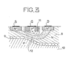
- FIG. 3 shows an exemplary embodiment in accordance with the invention.
- the layer 8 of type N in which the active zone is located, has an interface 9 (cross) with the rest of the substrate 10, of type P, situated at a depth which varies between source and drain so that said active zone has an increasing thickness from the source to the drain.
- This result can be obtained, for example, thanks to two successive diffusion operations, the first located on the drain side, and the following carried out on the entire surface.
- doped zones without N + , P + and N + reference points of source, gate and drain are produced, as shown in the drawing.
- Zone 11 filled with crosses shows the deserted zone when, in normal operation, the grid is reverse biased.
- the channel 12 under the grid can thus have an approximately constant width for the nominal operating conditions, which makes it possible to avoid having a very localized zone with very strong electric field. It is then possible to apply a higher voltage between drain and source, which allows obtaining higher powers.
- FIGS 4 and 5 show sections of Schottkty gate transistors according to the invention.
- the substrate 13 is insulating, for example in glass, or semi-insulating, for example in compensated gallium arsenide.
- a doped zone 14 of type N is produced on the surface of the latter.
- the source and drain electrodes have an ohmic type contact with this zone.
- the gate electrode constitutes a Schottky barrier.
- This doped area, which contains the active area, has an interface 15 with the rest of the substrate situated at a depth which varies so that said active area has an increasing thickness from the source to the drain.
- Such a configuration can be obtained by implantation.
- FIG. 6 schematically shows a series of operations making it possible to obtain a configuration in accordance with FIG. 4.
- a step 17 of a material is deposited (FIG. 6a) thickness is controlled with good precision.
- This material may be aluminum, and the step will be obtained by etching according to a known technique.
- the surface thus obtained is subjected to ion bombardment (arrows in FIG. 6b). They may be sulfur ions, or more advantageously silicon ions, accelerated to energies of the order of 200 to 300 keV.
- An N-type doped layer (18) is thus formed, the interface with the rest of the substrate reflecting the presence of the aluminum step.
- a localized chemical attack, before depositing the electrodes, makes it possible, if necessary, to obtain the configuration of FIG. 5, particularly favorable to the collection of charges, with a free face, that which carries the electrodes, in step.
- batteries of transistors such as that described above are housed on the same substrate with a square millimeter of surface, or of this order. These transistors are mounted in parallel for microwave amplification, in telecommunication devices in particular, on frequencies up to 20 gigahertz.
- the invention covers not only the variants described, but also all the other variants accessible to those skilled in the art from those described.
Landscapes
- Junction Field-Effect Transistors (AREA)
- Bipolar Transistors (AREA)
Applications Claiming Priority (2)
| Application Number | Priority Date | Filing Date | Title |
|---|---|---|---|
| FR7929764A FR2471049A1 (fr) | 1979-12-04 | 1979-12-04 | Transistor a effet de champ, procede de fabrication de celui-ci, et amplificateur comprenant un tel transistor |
| FR7929764 | 1979-12-04 |
Publications (2)
| Publication Number | Publication Date |
|---|---|
| EP0030178A2 true EP0030178A2 (de) | 1981-06-10 |
| EP0030178A3 EP0030178A3 (de) | 1981-07-01 |
Family
ID=9232375
Family Applications (1)
| Application Number | Title | Priority Date | Filing Date |
|---|---|---|---|
| EP80401623A Ceased EP0030178A3 (de) | 1979-12-04 | 1980-11-13 | Feld Effekt Transistor und Herstellung Verfahren |
Country Status (4)
| Country | Link |
|---|---|
| EP (1) | EP0030178A3 (de) |
| JP (1) | JPS5693374A (de) |
| FR (1) | FR2471049A1 (de) |
| NO (1) | NO803662L (de) |
Cited By (1)
| Publication number | Priority date | Publication date | Assignee | Title |
|---|---|---|---|---|
| EP0523593A1 (de) * | 1991-07-15 | 1993-01-20 | Motorola, Inc. | Feldeffekttransistor |
Family Cites Families (2)
| Publication number | Priority date | Publication date | Assignee | Title |
|---|---|---|---|---|
| DE2444489A1 (de) * | 1974-09-18 | 1976-04-01 | Heinz Prof Dr Rer Nat Beneking | Halbleiteranordnung und verfahren zu ihrer herstellung |
| DE2821975C2 (de) * | 1978-05-19 | 1983-01-27 | Siemens AG, 1000 Berlin und 8000 München | Metall-Halbleiter-Feldeffekttransistor (MESFET) und Verfahren zu dessen Herstellung |
-
1979
- 1979-12-04 FR FR7929764A patent/FR2471049A1/fr active Granted
-
1980
- 1980-11-13 EP EP80401623A patent/EP0030178A3/de not_active Ceased
- 1980-12-03 NO NO803662A patent/NO803662L/no unknown
- 1980-12-04 JP JP17145080A patent/JPS5693374A/ja active Pending
Cited By (3)
| Publication number | Priority date | Publication date | Assignee | Title |
|---|---|---|---|---|
| EP0523593A1 (de) * | 1991-07-15 | 1993-01-20 | Motorola, Inc. | Feldeffekttransistor |
| US5281839A (en) * | 1991-07-15 | 1994-01-25 | Motorola, Inc. | Semiconductor device having a short gate length |
| US5449628A (en) * | 1991-07-15 | 1995-09-12 | Motorola, Inc. | Method of making semiconductor device having a short gate length |
Also Published As
| Publication number | Publication date |
|---|---|
| EP0030178A3 (de) | 1981-07-01 |
| NO803662L (no) | 1981-06-05 |
| JPS5693374A (en) | 1981-07-28 |
| FR2471049B1 (de) | 1983-11-25 |
| FR2471049A1 (fr) | 1981-06-12 |
Similar Documents
| Publication | Publication Date | Title |
|---|---|---|
| EP0017531B1 (de) | Feldeffekttransistor mit hoher Grenzfrequenz und Verfahren zu dessen Herstellung | |
| EP0022388B1 (de) | Verfahren zur Herstellung eines vertikalen Feldeffekttransistors vom DMOS-Typ | |
| EP0061376A1 (de) | Planarer Feldeffekttransistor mit Elektroden aus metallisierten Löchern und Verfahren zur Herstellung des Transistors | |
| FR2700890A1 (fr) | Dispositif à transistor composé à effet de champ ayant une électrode de Schottky. | |
| EP4318597A1 (de) | Feldeffekttransistor mit p-fet-verhalten | |
| EP0045678B1 (de) | Laserquelle mit Halbleiterübergang, die Schottky-Dioden verwendet, und Herstellungsverfahren | |
| FR2689683A1 (fr) | Dispositif semiconducteur à transistors complémentaires. | |
| EP0051504B1 (de) | Feldeffekttransistor mit einem kurzen Kanal | |
| FR2568410A1 (fr) | Transistor statique a induction et son circuit integre | |
| EP0022001A1 (de) | Vertikaler Hochfrequenz-Leistungsfeldeffekttransistor und Verfahren zur Herstellung solch eines Transistors | |
| FR2745421A1 (fr) | Mesfet du type enrichissement | |
| EP0149390A2 (de) | Feldeffekttransistor mit vertikaler Sub-Mikronstruktur und Verfahren zu dessen Herstellung | |
| FR2696873A1 (fr) | Transistor à effet de champ et procédé pour sa fabrication. | |
| GB1589818A (en) | Field effect transistor and method for making same | |
| JPH0371794B2 (de) | ||
| EP0197838B1 (de) | Verfahren zum Herstellen eines Feldeffekttransistors mit selbstausrichtender Gate-Metallisierung | |
| FR2471049A1 (fr) | Transistor a effet de champ, procede de fabrication de celui-ci, et amplificateur comprenant un tel transistor | |
| EP0146430B1 (de) | Feldeffekttransistor mit regelbarer Schwellenspannung und integrierte Schaltung mit solchem Transistor | |
| US5311045A (en) | Field effect devices with ultra-short gates | |
| EP0083531B1 (de) | Gunndiodenähnliche unipolare Anordnung mit Elektronentransfer | |
| FR2572587A1 (fr) | Procede de fabrication d'un transistor a effet de champ du type a grille schottky | |
| FR2604828A1 (fr) | Procede de fabrication d'une diode p+nn+ et d'un transistor bipolaire comportant cette diode, utilisant l'effet de neutralisation des atomes donneurs par l'hydrogene atomique | |
| FR2466862A1 (fr) | Transistor a effet de champ et amplificateur pour hyperfrequences comprenant un tel transistor | |
| FR2607324A1 (fr) | Transistor a grille isolee avec diode verticale integree et procede de fabrication | |
| EP0145566B1 (de) | Leistungsfeldeffekttransistor und Verfahren zur Herstellung dieses Transistors |
Legal Events
| Date | Code | Title | Description |
|---|---|---|---|
| PUAI | Public reference made under article 153(3) epc to a published international application that has entered the european phase |
Free format text: ORIGINAL CODE: 0009012 |
|
| PUAL | Search report despatched |
Free format text: ORIGINAL CODE: 0009013 |
|
| AK | Designated contracting states |
Designated state(s): DE GB IT NL |
|
| AK | Designated contracting states |
Designated state(s): DE GB IT NL |
|
| 17P | Request for examination filed |
Effective date: 19810803 |
|
| STAA | Information on the status of an ep patent application or granted ep patent |
Free format text: STATUS: THE APPLICATION HAS BEEN REFUSED |
|
| 18R | Application refused |
Effective date: 19830818 |
|
| RIN1 | Information on inventor provided before grant (corrected) |
Inventor name: BERT, ALAIN |